EP4290583A2 - Method of making a semiconductor device - Google Patents
Method of making a semiconductor device Download PDFInfo
- Publication number
- EP4290583A2 EP4290583A2 EP23194255.8A EP23194255A EP4290583A2 EP 4290583 A2 EP4290583 A2 EP 4290583A2 EP 23194255 A EP23194255 A EP 23194255A EP 4290583 A2 EP4290583 A2 EP 4290583A2
- Authority
- EP
- European Patent Office
- Prior art keywords
- layer
- termination
- region
- dopant concentration
- area
- Prior art date
- Legal status (The legal status is an assumption and is not a legal conclusion. Google has not performed a legal analysis and makes no representation as to the accuracy of the status listed.)
- Pending
Links
Images


Classifications
-
- H—ELECTRICITY
- H10—SEMICONDUCTOR DEVICES; ELECTRIC SOLID-STATE DEVICES NOT OTHERWISE PROVIDED FOR
- H10D—INORGANIC ELECTRIC SEMICONDUCTOR DEVICES
- H10D30/00—Field-effect transistors [FET]
- H10D30/01—Manufacture or treatment
- H10D30/021—Manufacture or treatment of FETs having insulated gates [IGFET]
- H10D30/028—Manufacture or treatment of FETs having insulated gates [IGFET] of double-diffused metal oxide semiconductor [DMOS] FETs
- H10D30/0291—Manufacture or treatment of FETs having insulated gates [IGFET] of double-diffused metal oxide semiconductor [DMOS] FETs of vertical DMOS [VDMOS] FETs
-
- H—ELECTRICITY
- H10—SEMICONDUCTOR DEVICES; ELECTRIC SOLID-STATE DEVICES NOT OTHERWISE PROVIDED FOR
- H10D—INORGANIC ELECTRIC SEMICONDUCTOR DEVICES
- H10D62/00—Semiconductor bodies, or regions thereof, of devices having potential barriers
- H10D62/10—Shapes, relative sizes or dispositions of the regions of the semiconductor bodies; Shapes of the semiconductor bodies
- H10D62/102—Constructional design considerations for preventing surface leakage or controlling electric field concentration
- H10D62/103—Constructional design considerations for preventing surface leakage or controlling electric field concentration for increasing or controlling the breakdown voltage of reverse-biased devices
- H10D62/105—Constructional design considerations for preventing surface leakage or controlling electric field concentration for increasing or controlling the breakdown voltage of reverse-biased devices by having particular doping profiles, shapes or arrangements of PN junctions; by having supplementary regions, e.g. junction termination extension [JTE]
- H10D62/106—Constructional design considerations for preventing surface leakage or controlling electric field concentration for increasing or controlling the breakdown voltage of reverse-biased devices by having particular doping profiles, shapes or arrangements of PN junctions; by having supplementary regions, e.g. junction termination extension [JTE] having supplementary regions doped oppositely to or in rectifying contact with regions of the semiconductor bodies, e.g. guard rings with PN or Schottky junctions
- H10D62/107—Buried supplementary regions, e.g. buried guard rings
-
- H—ELECTRICITY
- H10—SEMICONDUCTOR DEVICES; ELECTRIC SOLID-STATE DEVICES NOT OTHERWISE PROVIDED FOR
- H10D—INORGANIC ELECTRIC SEMICONDUCTOR DEVICES
- H10D12/00—Bipolar devices controlled by the field effect, e.g. insulated-gate bipolar transistors [IGBT]
- H10D12/01—Manufacture or treatment
- H10D12/031—Manufacture or treatment of IGBTs
-
- H—ELECTRICITY
- H10—SEMICONDUCTOR DEVICES; ELECTRIC SOLID-STATE DEVICES NOT OTHERWISE PROVIDED FOR
- H10D—INORGANIC ELECTRIC SEMICONDUCTOR DEVICES
- H10D30/00—Field-effect transistors [FET]
- H10D30/60—Insulated-gate field-effect transistors [IGFET]
- H10D30/64—Double-diffused metal-oxide semiconductor [DMOS] FETs
- H10D30/66—Vertical DMOS [VDMOS] FETs
- H10D30/662—Vertical DMOS [VDMOS] FETs having a drift region having a doping concentration that is higher between adjacent body regions relative to other parts of the drift region
-
- H—ELECTRICITY
- H10—SEMICONDUCTOR DEVICES; ELECTRIC SOLID-STATE DEVICES NOT OTHERWISE PROVIDED FOR
- H10D—INORGANIC ELECTRIC SEMICONDUCTOR DEVICES
- H10D30/00—Field-effect transistors [FET]
- H10D30/60—Insulated-gate field-effect transistors [IGFET]
- H10D30/64—Double-diffused metal-oxide semiconductor [DMOS] FETs
- H10D30/66—Vertical DMOS [VDMOS] FETs
- H10D30/665—Vertical DMOS [VDMOS] FETs having edge termination structures
-
- H—ELECTRICITY
- H10—SEMICONDUCTOR DEVICES; ELECTRIC SOLID-STATE DEVICES NOT OTHERWISE PROVIDED FOR
- H10D—INORGANIC ELECTRIC SEMICONDUCTOR DEVICES
- H10D62/00—Semiconductor bodies, or regions thereof, of devices having potential barriers
- H10D62/10—Shapes, relative sizes or dispositions of the regions of the semiconductor bodies; Shapes of the semiconductor bodies
- H10D62/13—Semiconductor regions connected to electrodes carrying current to be rectified, amplified or switched, e.g. source or drain regions
- H10D62/149—Source or drain regions of field-effect devices
- H10D62/151—Source or drain regions of field-effect devices of IGFETs
- H10D62/156—Drain regions of DMOS transistors
- H10D62/157—Impurity concentrations or distributions
-
- H—ELECTRICITY
- H10—SEMICONDUCTOR DEVICES; ELECTRIC SOLID-STATE DEVICES NOT OTHERWISE PROVIDED FOR
- H10D—INORGANIC ELECTRIC SEMICONDUCTOR DEVICES
- H10D62/00—Semiconductor bodies, or regions thereof, of devices having potential barriers
- H10D62/10—Shapes, relative sizes or dispositions of the regions of the semiconductor bodies; Shapes of the semiconductor bodies
- H10D62/17—Semiconductor regions connected to electrodes not carrying current to be rectified, amplified or switched, e.g. channel regions
- H10D62/393—Body regions of DMOS transistors or IGBTs
-
- H—ELECTRICITY
- H10—SEMICONDUCTOR DEVICES; ELECTRIC SOLID-STATE DEVICES NOT OTHERWISE PROVIDED FOR
- H10D—INORGANIC ELECTRIC SEMICONDUCTOR DEVICES
- H10D62/00—Semiconductor bodies, or regions thereof, of devices having potential barriers
- H10D62/80—Semiconductor bodies, or regions thereof, of devices having potential barriers characterised by the materials
- H10D62/83—Semiconductor bodies, or regions thereof, of devices having potential barriers characterised by the materials being Group IV materials, e.g. B-doped Si or undoped Ge
- H10D62/832—Semiconductor bodies, or regions thereof, of devices having potential barriers characterised by the materials being Group IV materials, e.g. B-doped Si or undoped Ge being Group IV materials comprising two or more elements, e.g. SiGe
- H10D62/8325—Silicon carbide
-
- H—ELECTRICITY
- H10—SEMICONDUCTOR DEVICES; ELECTRIC SOLID-STATE DEVICES NOT OTHERWISE PROVIDED FOR
- H10W—GENERIC PACKAGES, INTERCONNECTIONS, CONNECTORS OR OTHER CONSTRUCTIONAL DETAILS OF DEVICES COVERED BY CLASS H10
- H10W10/00—Isolation regions in semiconductor bodies between components of integrated devices
- H10W10/01—Manufacture or treatment
- H10W10/031—Manufacture or treatment of isolation regions comprising PN junctions
-
- H—ELECTRICITY
- H10—SEMICONDUCTOR DEVICES; ELECTRIC SOLID-STATE DEVICES NOT OTHERWISE PROVIDED FOR
- H10W—GENERIC PACKAGES, INTERCONNECTIONS, CONNECTORS OR OTHER CONSTRUCTIONAL DETAILS OF DEVICES COVERED BY CLASS H10
- H10W10/00—Isolation regions in semiconductor bodies between components of integrated devices
- H10W10/30—Isolation regions comprising PN junctions
-
- H—ELECTRICITY
- H10—SEMICONDUCTOR DEVICES; ELECTRIC SOLID-STATE DEVICES NOT OTHERWISE PROVIDED FOR
- H10D—INORGANIC ELECTRIC SEMICONDUCTOR DEVICES
- H10D12/00—Bipolar devices controlled by the field effect, e.g. insulated-gate bipolar transistors [IGBT]
- H10D12/01—Manufacture or treatment
- H10D12/031—Manufacture or treatment of IGBTs
- H10D12/032—Manufacture or treatment of IGBTs of vertical IGBTs
-
- H—ELECTRICITY
- H10—SEMICONDUCTOR DEVICES; ELECTRIC SOLID-STATE DEVICES NOT OTHERWISE PROVIDED FOR
- H10D—INORGANIC ELECTRIC SEMICONDUCTOR DEVICES
- H10D12/00—Bipolar devices controlled by the field effect, e.g. insulated-gate bipolar transistors [IGBT]
- H10D12/411—Insulated-gate bipolar transistors [IGBT]
- H10D12/441—Vertical IGBTs
-
- H—ELECTRICITY
- H10—SEMICONDUCTOR DEVICES; ELECTRIC SOLID-STATE DEVICES NOT OTHERWISE PROVIDED FOR
- H10D—INORGANIC ELECTRIC SEMICONDUCTOR DEVICES
- H10D30/00—Field-effect transistors [FET]
- H10D30/60—Insulated-gate field-effect transistors [IGFET]
- H10D30/611—Insulated-gate field-effect transistors [IGFET] having multiple independently-addressable gate electrodes influencing the same channel
- H10D30/615—Insulated-gate field-effect transistors [IGFET] having multiple independently-addressable gate electrodes influencing the same channel comprising a MOS gate electrode and at least one non-MOS gate electrode
-
- H—ELECTRICITY
- H10—SEMICONDUCTOR DEVICES; ELECTRIC SOLID-STATE DEVICES NOT OTHERWISE PROVIDED FOR
- H10D—INORGANIC ELECTRIC SEMICONDUCTOR DEVICES
- H10D62/00—Semiconductor bodies, or regions thereof, of devices having potential barriers
- H10D62/10—Shapes, relative sizes or dispositions of the regions of the semiconductor bodies; Shapes of the semiconductor bodies
- H10D62/102—Constructional design considerations for preventing surface leakage or controlling electric field concentration
- H10D62/103—Constructional design considerations for preventing surface leakage or controlling electric field concentration for increasing or controlling the breakdown voltage of reverse-biased devices
- H10D62/105—Constructional design considerations for preventing surface leakage or controlling electric field concentration for increasing or controlling the breakdown voltage of reverse-biased devices by having particular doping profiles, shapes or arrangements of PN junctions; by having supplementary regions, e.g. junction termination extension [JTE]
- H10D62/106—Constructional design considerations for preventing surface leakage or controlling electric field concentration for increasing or controlling the breakdown voltage of reverse-biased devices by having particular doping profiles, shapes or arrangements of PN junctions; by having supplementary regions, e.g. junction termination extension [JTE] having supplementary regions doped oppositely to or in rectifying contact with regions of the semiconductor bodies, e.g. guard rings with PN or Schottky junctions
-
- H—ELECTRICITY
- H10—SEMICONDUCTOR DEVICES; ELECTRIC SOLID-STATE DEVICES NOT OTHERWISE PROVIDED FOR
- H10D—INORGANIC ELECTRIC SEMICONDUCTOR DEVICES
- H10D8/00—Diodes
- H10D8/01—Manufacture or treatment
- H10D8/051—Manufacture or treatment of Schottky diodes
-
- H—ELECTRICITY
- H10—SEMICONDUCTOR DEVICES; ELECTRIC SOLID-STATE DEVICES NOT OTHERWISE PROVIDED FOR
- H10D—INORGANIC ELECTRIC SEMICONDUCTOR DEVICES
- H10D8/00—Diodes
- H10D8/60—Schottky-barrier diodes
Definitions
- Breakdown voltage of a reverse-blocking junction is a factor that limits the reverse voltage a semiconductor device can withstand.
- a breakdown voltage close to its ideal limit e.g., about 90%
- avalanche breakdown can occur in such devices at a voltage substantially less than the ideal breakdown voltage because of excessively high electric fields that are present at high field points throughout the device.
- a high field point of a blocking junction under reverse bias may occur near (e.g., at) a metallurgical junction along a region of curvature, such as at the edge of unterminated junctions.
- Terminations regions or termination structures may include termination regions or termination structures (e.g., JTE (junction termination extension)) to mitigate the localization of high electric fields by laterally extending the depletion region away from the edges of the active regions, thereby increasing a voltage at which the breakdown may occur.
- termination structures are dopant sensitive and require masking or isolation during the fabrication of active area doped regions to prevent an unintentional alteration of the charge distribution in the termination structure and maintain proper blocking voltage.
- fabrication of regions configured to perform various functions threshold voltage adjustment regions, current spreading layers, barrier regions, or the like
- conventional doping schemes used to optimize the active area of the power device are typically incompatible with the termination regions.
- a power semiconductor device may include a first layer having a first conductivity type; a second layer disposed atop the first layer, the second layer having the first conductivity type; a termination region formed in the second layer, the termination region having a second conductivity type opposite the first type; and an active region at least partially formed in the second layer, wherein the active region is disposed adjacent to the termination region proximate a first side of the termination region and wherein the second layer is at least partially disposed adjacent to the termination region proximate a second side of the termination region opposite the first side.
- a semiconductor device may include a first layer having a first conductivity type; a second layer disposed atop the first layer, the second layer having the first conductivity type, wherein a dopant concentration profile of an average dopant concentration within the second layer as measured from a surface of the second layer to a given depth of the second layer comprises a retrograde profile; and a termination region formed in the second layer, the termination region having a second conductivity type opposite the first type, wherein the average dopant concentration of the second layer is greater than an average dopant concentration of the first layer.
- the inventive semiconductor device and method may advantageously provide a high voltage semiconductor device having a comparatively high breakdown voltage while allowing for an improvement in performance of an active region of the device. Moreover, such advantages may be realized without the additional processing steps of masking and patterning typically needed to isolate a termination region during conventional fabrication, thereby providing a simplified fabrication without sacrificing performance.
- the inventive semiconductor device and method described herein may be applicable to any semiconductor device, power semiconductor device or related configurations, for example such as, a junction field-effect transistor (JFET), insulated-gate bipolar transistor (IGBT), junction barrier Schottky (JBS) diode, merged PiN Schottky (MPS) diode, or the like.
- JFET junction field-effect transistor
- IGBT insulated-gate bipolar transistor
- JBS junction barrier Schottky
- MPS merged PiN Schottky
- the inventive concepts described herein may be advantageous in applications such as silicon carbide (SiC) related power semiconductor devices.
- FIG. 1 illustrates an exemplary conventional semiconductor device (device or power semiconductor device) 100.
- the device 100 generally includes a substrate 118 having a contact (e.g,. drain, cathode, etc.) 112, one or more layers (e.g., drift layer 116 shown) disposed atop the substrate 118 and one or more structures (e.g., gate 104 and source 106 shown) disposed atop the one or more layers/regions.
- An additional layer for example an optimization layer 102 (a threshold adjust layer, current spreading layers, JFET doping layer, p-barrier layer, or the like), is formed within the drift layer 116 beneath the gate 104 and source 106.
- an optimization layer 102 a threshold adjust layer, current spreading layers, JFET doping layer, p-barrier layer, or the like
- the additional charge associated with an optimization layer may, for example, allow for a reduction in on-resistances for the overall device and/or allow for an efficient scaling to higher voltages while maintaining optimized small pitch devices, thereby reducing cost and improving performance of the devices.
- termination structures e.g., termination region 114 or structures formed using such a region
- termination structures are dopant sensitive. That is, an unintentional alteration of the doped regions may have a negative effect on the ability of the termination structure to reduce electric fields within desired locations of the underlying device layers, thereby potentially decreasing a breakdown voltage of the entire device.
- conventional device fabrication processes and configuration requires the masking or isolation of the termination region from other selectively doped portions of the device to avoid such an alteration of the dopant profile.
- the optimization layer 102, wells 108, 110, gate 104 and source 103,105 are confined within an active area or active region 110 of the device 100 and the termination region 114 disposed outside of the active area 110.
- the active region 110 may be defined as a region of the semiconductor device 100) which facilitate desired functions controlled conduction or switching on/off of the semiconductor device.
- the formation of the active region 110 typically requires multiple depositions of, for example, material layers (e.g., silicon, silicon carbide, oxides, or the like) diffusion, implant or etch masks, followed by subsequent etch processes (e.g., wet etch, mesa etch, or the like).
- material layers e.g., silicon, silicon carbide, oxides, or the like
- etch processes e.g., wet etch, mesa etch, or the like.
- the termination region 233, active region 232 and second layer 222 may be disposed with respect to one another in any manner suitable for an intended application of the device 220.
- the second layer 222 may extend from the active region 232 at least partially, or in some embodiments fully, across the device 220 to an area 244 beyond an opposing side of the termination region 233.
- the active region 232 may be disposed adjacent to the termination region 233 proximate a first side 238 of the termination region 233 and the second layer 222 is at least partially disposed adjacent to the termination region 233 proximate a second side 228 of the termination region 233 opposite the first side 238.
- the inventors have observed that extending the second layer 222 at least partially across the device 220 allows for both the separate functional regions of the device to operate properly, for example, the active region 232 and termination region 233, to be fabricated without the additional processing steps of masking and patterning typically required to isolate the second layer 222 from the termination region or structure in conventional device fabrication processes (e.g., as described above).
- the second layer 222 may be formed via a blanket deposition and/or doping process (e.g., a deposition process without the use of etch or patterning masks, subsequent etch processes related to such masks, or the like).
- the first layer 234 and second layer 222 each may be any type of layer suitable for device 220 construction and may be dependent on an intended application of the device 220.
- the first layer 234 may be a drift layer, barrier layer, buffer layer, or the like.
- the second layer 222 may be an optimization layer, threshold adjust layer, JFET layer, current spreading layer (CSL), hole barrier layer, or the like.
- first layer 234 and second layer 222 may be formed via any suitable fabrication process, for example, deposition, epitaxial growth, or the like.
- the second layer 222 may be formed from at least a portion of the first layer 234.
- at least a portion of the first layer 234 may be selectively doped to a desired depth to form the second layer 222.
- Each of the first layer 234 and second layer 222 may be fabricated from any materials suitable for an intended application of the device 220 and may be fabricated from similar materials, or in some embodiments, different materials.
- each of the first layer 234 and second layer 222 may comprise silicon (Si), silicon carbide (SiC), or the like.
- the active area 232 generally includes one or more structures configured to facilitate the desired functions of the semiconductor device (e.g., voltage blocking, switching, or the like).
- the active area 232 may include a well or body (collectively well 226), the gate 246, source contact 230, or the like.
- the termination region 233 may include or more termination structures 224 suitable to provide a desired blocking voltage.
- the termination region 233 may include a floating guard ring, junction termination extension (JTE) structure (e.g., single-zone JTE, multiple zone JTE, space modulated JTE, or the like), or the like.
- JTE junction termination extension
- the termination region may extend substantially through, or in some embodiments, completely through, the second layer 222 to the first layer 234, for example such as shown at 240.
- the dopant concentration or average dopant concentration of the second layer 222 may be higher than that of the first layer 234.
- a dopant concentration or average dopant concentration of the second layer 222 may be between about two (2) times to about fifteen (15) times greater than that of the first layer 234.
- the first layer 234 and second layer 222 may each comprise an n-type conductivity and the termination region a p-type conductivity.
- the inventors have observed that the above described relative doping of the first layer 234, second layer 222 and termination region 233 allows for the second layer 222 to be formed via a deposition, implantation or diffusion process (e.g., a blanket deposition, implant or diffusion process) while eliminating the need for additional processing steps (e.g., masking, patterning and etching steps) that are typically required to isolate the termination region during conventional device fabrication, thereby providing a device 220 that may be fabricated in a comparatively simpler and/or efficient process while maintaining desired performance characteristics of the device 220 (e.g., a high breakdown voltage).
- a deposition, implantation or diffusion process e.g., a blanket deposition, implant or diffusion process
- additional processing steps e.g., masking, patterning and etching steps
- such a fabrication process may allow for the utilization of high-energy implantations, thereby providing deep range doping profiles without the need for conventionally high cost high-stopping power masking layers (e.g., such as metal or thick-oxide hardmasks).
- the termination region 233 may be non-continuous and/or include a plurality of discrete or separated regions (e.g., segmented).
- the semiconductor device (device) 300 may comprise a termination region 320 having a termination structure, for example a JTE, which includes a plurality of discrete doped regions 321.
- the regions 321 may be of any size and distribution suitable to provide a desired dopant profile across the termination region 320 and may be dependent on process capabilities, a desired dopant profile, or the like.
- the device 300 may include one or more layers, for example such as a first layer 314 and second layer 318 (e.g., similar to the first layer 234 and second layer 222 described above) disposed above a substrate 302 (e.g., similar to the substrate 242 described above).
- a substrate 302 e.g., similar to the substrate 242 described above.
- One or more regions for example, an active region 336 having a well or body (collectively well 316) may be formed in the second layer 318.
- the active region 336 and well 316 may be similar in structure and function to the active area 232 and well 226 described above.
- the active region 336 and termination region 320 may be disposed with respect to one another in any manner suitable to achieve desired performance characteristics of the device 300.
- the well 316 of the active region 336 may be disposed adjacent to, or in direct contact with, one or more of the regions 321.
- a portion of the second layer 318 may be disposed between at least a portion of the well 316 and one or more of the regions 321 (e.g., such as shown in phantom at 360).
- the first layer 314, second layer 318 and termination region 320 may be doped relative to one another in any manner suitable to fabricate the device 300 while maintaining desired performance of the device 300, for example, such as described above with respect to the first layer 234, second layer 222 and termination region 233 of FIG. 2 .
- the discrete regions 321 may be similarly doped with respect to dopant type and concentration, or alternatively, may comprise varying dopant concentrations across the termination region 320.
- the discrete regions 321 may be doped so as to have an effective doping profile that generally decreases along a direction away from an edge 330 of termination region 320.
- the decrease in doping concentration may be a macro-variation such that the dopant concentration within each discrete region 321 is consistent, but the spacing between the doped regions varies, thereby decreasing the overall dopant concentration as the distance away from the edge 330 increases.
- varying concentration it is meant that the dopant amount or density of the regions varies, and it is this variance that defines the effective dose.
- effective dose is the fraction of the termination region 320 area that is open to receive the dopants (implants) versus a total area being sampled.
- the second layer may comprise any dopant profile suitable to allow for the simultaneous desired performance of both the active region and termination region (a "compensated termination design").
- a depth and doping of the second layer within the termination region e.g., termination region 232 of FIG. 2 or termination region 320 of FIG.
- a sheet doping concentration within the second layer may be between about 2 ⁇ 10 12 cm -2 and about 8 ⁇ 10 12 cm -2 .
- a dopant concentration proximate a surface of the second layer is less than a dopant concentration at depths further away from the surface.
- an average dopant concentration at a depth of at least 0.2 ⁇ m from the surface of the second layer may be at least four (4) times greater than that of an average dopant concentration at the surface of the second layer.
- a doping concentration proximate or at the surface of the second layer may be about 8 ⁇ 10 15 cm -3 to about 2 ⁇ 10 16 cm -3 , or in some embodiments, an average dopant concentration of up to about 1 ⁇ 10 16 cm -3 , and an average dopant concentration at a depth greater than about 0.2 ⁇ m from the surface into the second layer may be about 5 ⁇ 10 16 cm -3 to about 1 ⁇ 10 17 cm -3 .
- a sheet doping concentration in the second layer within an area defined as between the surface of the second layer to a depth of about 1.5 ⁇ m may be between about 2 ⁇ 10 12 cm -2 to about 5 ⁇ 10 12 cm -2 . Any of the above described concentrations may be implemented via a profile, wherein the concentration increases from the surface to the depth in the second layer using, for example, an implanted process or with a "step-wise" profile having an increasing doping concentration of distinct epitaxial layers.
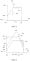
- FIG. 4 illustrates a graph 400 of one such dopant profile of the second layer.
- the graph 400 schematically depicts a retrograde dopant profile 402 of the second layer, shown as a function of a dopant concentration (y-axis) 406 and depth (x-axis) 404 of the second layer.
- a dopant concentration of the second layer may increase from a first dopant concentration 408 proximate the surface (indicated graphically at 418) to a peak dopant concentration 412 at a first depth 414 of the second layer, thereby giving a retrograde dopant profile 402.
- the dopant concentration may remain approximately constant, or alternatively, vary or oscillate about the peak dopant concentration 412 (as shown at 413) until a maximum depth 416, where it then decreases to reach the doping concentration of the first layer (e.g., first layer 234, 314).
- the maximum depth 416 may be any depth up to the thickness of the second layer, for example, such as greater than or equal to a depth of other components or regions of the device (e.g., wells, body, active area, termination area, or the like).
- the first dopant concentration 408 may be about 5 ⁇ 10 15 cm -3 to about 5 ⁇ 10 16 cm -3 , or in some embodiments, about 8 ⁇ 10 15 cm -3 to about 2 ⁇ 10 16 cm -3 .
- the peak dopant concentration 412 may be any dopant concentration that is greater than the first dopant concentration 408.
- the peak dopant concentration 412 may be about four (4) to about ten (10) times greater than the first dopant concentration 408.
- the depth (first depth 414) at which the peak dopant concentration is reached may be any depth suitable to achieve a desired dopant profile and may be dependent on, for example, a thickness of the second layer, material composition of the second layer and other layers disposed adjacent to the second layer, size shape and placement of other components or regions of the device (e.g., wells, body, active area, termination area, or the like).
- a doping concentration of the second layer is less than about 20% of a doping concentration of a well formed in the active area (e.g., well 226 or well 316 described above) at substantially similar depths into the second layer and well region until such a depth where the well region reaches a peak concentration.
- the peak dopant concentration 412 may be reached at depth of about 0.15um to 0.3um from the surface of the second layer.
- the dopant concentration increase is shown as having a constant slope 410, the increase of dopant concentration may be exponential, logarithmic, or the like.
- the slope 410 may be dependent on a desired dopant amount as it relates to the dopant profiles of other components of other components or regions of the device (e.g., well 226 or termination region 233 described above, or the like), thereby allowing for an optimal dopant concentration of each component or region simultaneously to achieve a desired performance of the device (e.g., threshold voltage, etc.).
- the retrograde profile 402 shown in FIG. 4 allows for a maximization of an effective sheet doping concentration of the second layer while minimizing impact on surface doping concentration of other regions in the active and termination regions of the device, thereby allowing for such a maximization (and achieving optimization layer features like reducing on-resistance in devices like JFETs, MOSFETs etc.) without affecting other device parameters (e.g., channel length, threshold voltage, or the like) that depend upon the net dopant concentration at the surface of the second layer and other layers or components (e.g., p-well, p-body, termination, etc.).
- device parameters e.g., channel length, threshold voltage, or the like
- any of the regions or components formed within the second layer may include similar dopant profiles.
- the well 226 e.g., p-well
- the retrograde dopant profile of the well 226 may include a profile such that a dopant concentration that increases by at least five (5) times from a surface of the well region to a depth at which a peak concentration is disposed.
- FIG. 5 depicts a retrograde dopant profile 502 of the second layer similar to that described above in addition to possible termination or well regions (e.g., termination region 233 or termination region 320, well region 226, well region 316 described above) dopant profiles (shown at 522 and 524), in accordance with some embodiments of the present invention.
- Each dopant profile is shown as a function of a dopant concentration (y-axis) 506 and depth (x-axis) 504 of the respective layer or region the dopant profile represents.
- the retrograde dopant profile 502 is similar, or in some embodiments the same, as the retrograde profile 402 described above and the embodiments thereof.
- Each of the retrograde dopant profile 502 of the second layer and dopant profiles 522, 524 of the termination or well region may depict dopant concentrations of an opposing type.
- the retrograde dopant profile 502 of the second layer may represent a p-type dopant concentration within the second layer and the dopant profiles 522, 524 of the termination or well regions represent an n-type dopant concentration within the termination region.
- the termination or well region dopant profiles may be a retrograde profile, box-like profile, or the like.
- the termination region dopant profile 522 may increase from a first dopant concentration 526 proximate the surface or top surface (indicated graphically at 520) to a peak dopant concentration 528 at a first depth 530 of the termination or well regions, thereby giving a retrograde dopant profile 522.
- the peak dopant concentration is higher than the peak concentration (e.g., peak concentration 412, 413 described above) of the second layer.
- the dopant concentration may remain approximately constant, or alternatively, vary or oscillate about the peak dopant concentration 528 until a second depth 532, where it decreases to a second dopant concentration 538 at a maximum depth 516.
- the maximum depth 516, wherein the second layer doping concentration is proximal to the first layer 234 doping concentration may be any depth up to the thickness of the termination region, for example, such as greater than or equal to a depth of other components or regions of the device (e.g., wells, body, active area, termination area, second layer or the like).
- the termination region dopant profile 524 may remain constant, or oscillate about, a first dopant concentration 534 from proximate the surface 520 to a third depth 542, where it then decreases to a third dopant concentration 540 at the maximum depth 516.
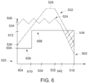
- the dopant profile of the second layer 402, 502 described above with respect to FIGS. 4 and 5 may at least partially include a "step" like profile including one or more plateaus 606, 608, for example, such as the dopant profile 602 shown in FIG. 6 .
- the dopant profile 602 may include a first dopant concentration 604 proximate the surface of the second layer (indicated graphically at 520) of the second layer.
- the first dopant concentration 604 may remain substantially constant to a first depth 610.
- the dopant concentration may increase to a peak dopant concentration 612.
- the dopant concentration may remain approximately constant, or alternatively, vary or oscillate about the peak dopant concentration 612 until the maximum depth 516, where it decreases to the first layer 234 doping concentration.
- the first dopant concentration 604 may be about 5 ⁇ 10 15 cm -3 to about 5 ⁇ 10 16 cm -3 , or in some embodiments, about 8 ⁇ 10 15 cm -3 to about 2 ⁇ 10 16 cm -3 .
- the peak dopant concentration 612 may be any dopant concentration that is greater than the first dopant concentration 604. For example, in some embodiments, the peak dopant concentration 612 may be about four (4) to about ten (10) times greater than the first dopant concentration 604.
- the depth (first depth 610) at which the peak dopant concentration is reached may be any depth suitable to achieve a desired dopant profile and may be dependent on, for example, a thickness of the second layer, material composition of the second layer and other layers disposed adjacent to the second layer, size shape and placement of other components or regions of the device (e.g., wells, body, active area, termination area, or the like).
- the peak dopant concentration 612 may be reached at depth of about 0.15um to 0.3um from the surface of the second layer.
- the depth and doping of the second layer within the termination region may be such that a sheet doping concentration of the first type in the second layer located beneath the termination region of the second type (e.g., in the first layer and second layer in embodiments where the second layer is at least partially disposed beneath the termination region) is limited by a critical charge of the material utilized.
- the sheet doping concentration of the first type beneath the termination region may be less than about 1.1 ⁇ 10 13 cm -2 .
- the sheet doping concentration of the portion of the second layer located below the termination region (indicated by the shaded region 536 in FIGS. 5 and 6 ) may be 5 ⁇ 10 11 cm -2 to 5 ⁇ 10 12 cm -2 .
- the sheet doping concentration of the portion of the second layer located below the termination region may be 7.5 ⁇ 10 11 cm -2 to 1.25 ⁇ 10 12 cm -2 .
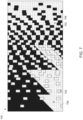
- FIG. 7 is an example of top-down image of a portion of termination region 700 in accordance with some embodiments of the present invention.
- the termination region 700 is graded (e.g., laterally varying the percentage of implanted percentage of the top-down layout) and segmented (e.g., as described above with respect to FIG. 3 ).
- the termination region 700 may include p-type areas 706 (e.g., p-type areas formed via local doping e.g. implantation or diffusion, as in FIG 3 , region 321)) and n-type areas 702 (e.g., n-type areas formed via, fabrication of the second layer 222, 338 described above).
- the termination region 700 may maintain a comparable blocking voltage as un-compensated termination (>90% 1D limit) with an additional, for example, about 30%, compensated dose (e.g., about 3 ⁇ 10 12 cm -2 to about 4 ⁇ 10 12 cm -2 ).
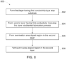
- FIG. 8 depicts a method 800 for fabricating a semiconductor device in accordance with some embodiments of the present invention.
- the second layer may be any type of layer, for example, such as the second layer 238, 318 described above.
- the second layer may have a conductivity type (e.g., n-type or p-type) the same as that of the first layer.
- the second layer may have a total or effective dopant concentration higher than that of the first layer.
- the second layer may include a dopant profile similar to the dopant profiles 402, 502, 602 described above.
Landscapes
- Electrodes Of Semiconductors (AREA)
- Junction Field-Effect Transistors (AREA)
- Thyristors (AREA)
- Bipolar Transistors (AREA)
- Thin Film Transistor (AREA)
Abstract
Description
- The subject matter disclosed herein relates to semiconductor devices and, more particularly, to silicon carbide (SiC)-based semiconductor devices.
- Breakdown voltage of a reverse-blocking junction is a factor that limits the reverse voltage a semiconductor device can withstand. A breakdown voltage close to its ideal limit (e.g., about 90%) is a critical performance metric for power devices, particularly high-voltage devices such as silicon carbide devices. However, avalanche breakdown can occur in such devices at a voltage substantially less than the ideal breakdown voltage because of excessively high electric fields that are present at high field points throughout the device. For example, a high field point of a blocking junction under reverse bias may occur near (e.g., at) a metallurgical junction along a region of curvature, such as at the edge of unterminated junctions.
- Conventional devices may include termination regions or termination structures (e.g., JTE (junction termination extension)) to mitigate the localization of high electric fields by laterally extending the depletion region away from the edges of the active regions, thereby increasing a voltage at which the breakdown may occur. However, such termination structures are dopant sensitive and require masking or isolation during the fabrication of active area doped regions to prevent an unintentional alteration of the charge distribution in the termination structure and maintain proper blocking voltage. For example, fabrication of regions configured to perform various functions (threshold voltage adjustment regions, current spreading layers, barrier regions, or the like) within the active areas of the device require masking and etching steps and are likewise limited to low energy implants to prevent dopants from unintentionally impinging on the termination structure. Moreover, conventional doping schemes used to optimize the active area of the power device are typically incompatible with the termination regions.
- Therefore the inventors have provided an improved semiconductor device and method of making thereof.
- Embodiments of a semiconductor device and methods of forming thereof are provided herein. In some embodiments, a power semiconductor device may include a first layer having a first conductivity type; a second layer disposed atop the first layer, the second layer having the first conductivity type; a termination region formed in the second layer, the termination region having a second conductivity type opposite the first type; and an active region at least partially formed in the second layer, wherein the active region is disposed adjacent to the termination region proximate a first side of the termination region and wherein the second layer is at least partially disposed adjacent to the termination region proximate a second side of the termination region opposite the first side.
- In some embodiments, a semiconductor device may include a first layer having a first conductivity type; a second layer disposed atop the first layer, the second layer having the first conductivity type, wherein a dopant concentration profile of an average dopant concentration within the second layer as measured from a surface of the second layer to a given depth of the second layer comprises a retrograde profile; and a termination region formed in the second layer, the termination region having a second conductivity type opposite the first type, wherein the average dopant concentration of the second layer is greater than an average dopant concentration of the first layer.
- In some embodiments, a method for forming a semiconductor device may include forming a first layer having a first conductivity type atop a substrate; forming a second layer having the first conductivity type atop the first layer via a blanket fabrication process; doping the second layer such that an average dopant concentration of the second layer is greater than an average dopant concentration of the first layer; and forming a termination area doped region in the second layer, the termination area doped region having a second conductivity type opposite the first type.
- These and other features, aspects, and advantages of the present disclosure will become better understood when the following detailed description is read with reference to the accompanying drawings in which like characters represent like parts throughout the drawings, wherein:
-
FIG. 1 illustrates a cross-sectional view of a conventional semiconductor or metal oxide semiconductor (MOS) device; -
FIG. 2 illustrates a cross-sectional view of a semiconductor MOS device in accordance with some embodiments of the present invention; -
FIG. 3 illustrates a cross-sectional view of a semiconductor device in accordance with some embodiments of the present invention; -
FIG. 4 illustrates an exemplary dopant profile for at least a portion of the semiconductor device depicted inFIGS. 2 and 3 in accordance with some embodiments of the present invention; -
FIG. 5 illustrates an exemplary dopant profile for at least a portion of the semiconductor device depicted inFIGS. 2 and 3 in accordance with some embodiments of the present invention; -
FIG. 6 illustrates an exemplary dopant profile for at least a portion of the semiconductor device depicted inFIGS. 2 and 3 in accordance with some embodiments of the present invention; -
FIG. 7 illustrates a top-down view of an embodiment of the termination region depicted inFIGS. 2 and 3 in accordance with some embodiments of the present invention; and -
FIG. 8 depicts a method for forming a semiconductor device in accordance with some embodiments of the present invention. - Unless otherwise indicated, the drawings provided herein are meant to illustrate features of embodiments of the disclosure. These features are believed to be applicable in a wide variety of systems comprising one or more embodiments of the disclosure. As such, the drawings are not meant to include all conventional features known by those of ordinary skill in the art to be required for the practice of the embodiments disclosed herein.
- Embodiments of a semiconductor device and methods of forming thereof are provided herein. In at least some embodiments, the inventive semiconductor device and method may advantageously provide a high voltage semiconductor device having a comparatively high breakdown voltage while allowing for an improvement in performance of an active region of the device. Moreover, such advantages may be realized without the additional processing steps of masking and patterning typically needed to isolate a termination region during conventional fabrication, thereby providing a simplified fabrication without sacrificing performance.
- Although described in the context of a metal-oxide-semiconductor field-effect transistor (MOSFET) having a particular configuration, the inventive semiconductor device and method described herein may be applicable to any semiconductor device, power semiconductor device or related configurations, for example such as, a junction field-effect transistor (JFET), insulated-gate bipolar transistor (IGBT), junction barrier Schottky (JBS) diode, merged PiN Schottky (MPS) diode, or the like. In some embodiments, the inventors have observed that the inventive concepts described herein may be advantageous in applications such as silicon carbide (SiC) related power semiconductor devices.
-
FIG. 1 illustrates an exemplary conventional semiconductor device (device or power semiconductor device) 100. Thedevice 100 generally includes asubstrate 118 having a contact (e.g,. drain, cathode, etc.) 112, one or more layers (e.g.,drift layer 116 shown) disposed atop thesubstrate 118 and one or more structures (e.g.,gate 104 andsource 106 shown) disposed atop the one or more layers/regions. An additional layer, for example an optimization layer 102 (a threshold adjust layer, current spreading layers, JFET doping layer, p-barrier layer, or the like), is formed within thedrift layer 116 beneath thegate 104 andsource 106. The inventors have observed that the additional charge associated with an optimization layer may, for example, allow for a reduction in on-resistances for the overall device and/or allow for an efficient scaling to higher voltages while maintaining optimized small pitch devices, thereby reducing cost and improving performance of the devices. - In addition, at least partially formed in the
drift layer 116 and/or the optimization layer 102 are one or more well regions (e.g., twowell regions 108, 120 and two nestedn+ source regions drift layer 116 further includes atermination region 114 formed within thedrift layer 116 and adjacent to thewells 108, 120. - The inventors have observed that in conventional device configuration and fabrication, termination structures (e.g.,
termination region 114 or structures formed using such a region) are dopant sensitive. That is, an unintentional alteration of the doped regions may have a negative effect on the ability of the termination structure to reduce electric fields within desired locations of the underlying device layers, thereby potentially decreasing a breakdown voltage of the entire device. As such, conventional device fabrication processes and configuration requires the masking or isolation of the termination region from other selectively doped portions of the device to avoid such an alteration of the dopant profile. - For example, as can be seen in
FIG. 1 , the optimization layer 102,wells gate 104 and source 103,105 are confined within an active area oractive region 110 of thedevice 100 and thetermination region 114 disposed outside of theactive area 110. Such a configuration allows for isolation of thetermination region 114, thereby reducing instances of unintentional doping of thetermination region 114. As used herein, theactive region 110 may be defined as a region of the semiconductor device 100) which facilitate desired functions controlled conduction or switching on/off of the semiconductor device. - To achieve the above described isolation of the
termination region 114, conventional device fabrication processes require multiple deposition, patterning, and etch steps. For example, the formation of theactive region 110 typically requires multiple depositions of, for example, material layers (e.g., silicon, silicon carbide, oxides, or the like) diffusion, implant or etch masks, followed by subsequent etch processes (e.g., wet etch, mesa etch, or the like). - Referring to
FIG. 2 , thesemiconductor device 220 may generally comprise afirst layer 234, asecond layer 222 disposed above thefirst layer 234, and atermination region 233 and an active area oractive region 232 each at least partially formed in thesecond layer 222. In some embodiments, one or more structures (e.g.,gate 246 andsource contact 230 shown) may be disposed above thefirst layer 234 andsecond layer 222. In some embodiments, asubstrate 242 having a contact (e.g. drain, cathode, etc.) 236 may be disposed beneath thefirst layer 234. When present, thesubstrate 242 may be any type of substrate and comprised of any materials suitable for an intended application of thedevice 220. For example, in some embodiments, thesubstrate 242 may be a silicon (Si) or silicon carbide (SiC) containing substrate. - The
termination region 233,active region 232 andsecond layer 222 may be disposed with respect to one another in any manner suitable for an intended application of thedevice 220. For example, in some embodiments, thesecond layer 222 may extend from theactive region 232 at least partially, or in some embodiments fully, across thedevice 220 to anarea 244 beyond an opposing side of thetermination region 233. For example, in such embodiments, theactive region 232 may be disposed adjacent to thetermination region 233 proximate afirst side 238 of thetermination region 233 and thesecond layer 222 is at least partially disposed adjacent to thetermination region 233 proximate asecond side 228 of thetermination region 233 opposite thefirst side 238. - The inventors have observed that extending the
second layer 222 at least partially across thedevice 220 allows for both the separate functional regions of the device to operate properly, for example, theactive region 232 andtermination region 233, to be fabricated without the additional processing steps of masking and patterning typically required to isolate thesecond layer 222 from the termination region or structure in conventional device fabrication processes (e.g., as described above). For example, thesecond layer 222 may be formed via a blanket deposition and/or doping process (e.g., a deposition process without the use of etch or patterning masks, subsequent etch processes related to such masks, or the like). - The
first layer 234 andsecond layer 222 each may be any type of layer suitable fordevice 220 construction and may be dependent on an intended application of thedevice 220. For example, in some embodiments, thefirst layer 234 may be a drift layer, barrier layer, buffer layer, or the like. In another example, in some embodiments, thesecond layer 222 may be an optimization layer, threshold adjust layer, JFET layer, current spreading layer (CSL), hole barrier layer, or the like. - Each of the
first layer 234 andsecond layer 222 may be formed via any suitable fabrication process, for example, deposition, epitaxial growth, or the like. In addition, in some embodiments, thesecond layer 222 may be formed from at least a portion of thefirst layer 234. For example, in such embodiments, at least a portion of thefirst layer 234 may be selectively doped to a desired depth to form thesecond layer 222. - Each of the
first layer 234 andsecond layer 222 may be fabricated from any materials suitable for an intended application of thedevice 220 and may be fabricated from similar materials, or in some embodiments, different materials. For example, in some embodiments, each of thefirst layer 234 andsecond layer 222 may comprise silicon (Si), silicon carbide (SiC), or the like. - The
active area 232 generally includes one or more structures configured to facilitate the desired functions of the semiconductor device (e.g., voltage blocking, switching, or the like). For example, in some embodiments, theactive area 232 may include a well or body (collectively well 226), thegate 246,source contact 230, or the like. - The
termination region 233 may include ormore termination structures 224 suitable to provide a desired blocking voltage. For example, in some embodiments, thetermination region 233 may include a floating guard ring, junction termination extension (JTE) structure (e.g., single-zone JTE, multiple zone JTE, space modulated JTE, or the like), or the like. Although shown as extending partially through thesecond layer 222, the termination region may extend substantially through, or in some embodiments, completely through, thesecond layer 222 to thefirst layer 234, for example such as shown at 240. - The
first layer 234,second layer 222 andtermination region 233 may be doped relative to one another in any manner suitable to fabricate thedevice 220 while maintaining desired performance of thedevice 220. For example, in some embodiments, thefirst layer 234,second layer 222 andtermination region 233 may each comprise a dopant having a sufficient dopant concentration such that each of thefirst layer 234 andsecond layer 222 are of the same conductivity type (e.g., n-type or p-type) and thetermination region 233 is of an opposite conductivity type (e.g., n-type or p-type) compared to that of thefirst layer 234 andsecond layer 222. In such embodiments, the dopant concentration or average dopant concentration of thesecond layer 222 may be higher than that of thefirst layer 234. For example, in some embodiments, a dopant concentration or average dopant concentration of thesecond layer 222 may be between about two (2) times to about fifteen (15) times greater than that of thefirst layer 234. In one exemplary embodiment of the relative doping described above, thefirst layer 234 andsecond layer 222 may each comprise an n-type conductivity and the termination region a p-type conductivity. - The inventors have observed that the above described relative doping of the
first layer 234,second layer 222 andtermination region 233 allows for thesecond layer 222 to be formed via a deposition, implantation or diffusion process (e.g., a blanket deposition, implant or diffusion process) while eliminating the need for additional processing steps (e.g., masking, patterning and etching steps) that are typically required to isolate the termination region during conventional device fabrication, thereby providing adevice 220 that may be fabricated in a comparatively simpler and/or efficient process while maintaining desired performance characteristics of the device 220 (e.g., a high breakdown voltage). Moreover, such a fabrication process may allow for the utilization of high-energy implantations, thereby providing deep range doping profiles without the need for conventionally high cost high-stopping power masking layers (e.g., such as metal or thick-oxide hardmasks). - Although shown as a contiguous layer in
FIG. 2 , thetermination region 233 may be non-continuous and/or include a plurality of discrete or separated regions (e.g., segmented). For example, referring toFIG. 3 , in some embodiments the semiconductor device (device) 300 may comprise atermination region 320 having a termination structure, for example a JTE, which includes a plurality of discrete dopedregions 321. Theregions 321 may be of any size and distribution suitable to provide a desired dopant profile across thetermination region 320 and may be dependent on process capabilities, a desired dopant profile, or the like. - In some embodiments, the
device 300 may include one or more layers, for example such as afirst layer 314 and second layer 318 (e.g., similar to thefirst layer 234 andsecond layer 222 described above) disposed above a substrate 302 (e.g., similar to thesubstrate 242 described above). One or more regions, for example, anactive region 336 having a well or body (collectively well 316) may be formed in thesecond layer 318. When present, theactive region 336 and well 316 may be similar in structure and function to theactive area 232 and well 226 described above. - The
active region 336 andtermination region 320 may be disposed with respect to one another in any manner suitable to achieve desired performance characteristics of thedevice 300. For example, in some embodiments, the well 316 of theactive region 336 may be disposed adjacent to, or in direct contact with, one or more of theregions 321. Alternatively or on combination, in some embodiments, a portion of thesecond layer 318 may be disposed between at least a portion of the well 316 and one or more of the regions 321 (e.g., such as shown in phantom at 360). - The
first layer 314,second layer 318 andtermination region 320 may be doped relative to one another in any manner suitable to fabricate thedevice 300 while maintaining desired performance of thedevice 300, for example, such as described above with respect to thefirst layer 234,second layer 222 andtermination region 233 ofFIG. 2 . - Within the
termination region 320, thediscrete regions 321 may be similarly doped with respect to dopant type and concentration, or alternatively, may comprise varying dopant concentrations across thetermination region 320. For example, in some embodiments, thediscrete regions 321 may be doped so as to have an effective doping profile that generally decreases along a direction away from anedge 330 oftermination region 320. In some embodiments, the decrease in doping concentration may be a macro-variation such that the dopant concentration within eachdiscrete region 321 is consistent, but the spacing between the doped regions varies, thereby decreasing the overall dopant concentration as the distance away from theedge 330 increases. It should be noted that by "varying concentration", it is meant that the dopant amount or density of the regions varies, and it is this variance that defines the effective dose. As used here, "effective dose" is the fraction of thetermination region 320 area that is open to receive the dopants (implants) versus a total area being sampled. - In any of the above embodiments, the second layer (e.g.,
second layer 222 ofFIG. 2 orsecond layer 318 ofFIG. 3 ) may comprise any dopant profile suitable to allow for the simultaneous desired performance of both the active region and termination region (a "compensated termination design"). For example, in some embodiments, a depth and doping of the second layer within the termination region (e.g.,termination region 232 ofFIG. 2 ortermination region 320 ofFIG. 3 ) may be such that a total integrated net n-type dopant charge located beneath the termination region (and second layer in embodiments where the second layer is at least partially disposed beneath the termination region) is limited by a critical charge of the material utilized (e.g., a sheet doping concentration of about 1.1×1013cm-2 in embodiments where SiC is utilized). In such embodiments, a sheet doping concentration within the second layer may be between about 2×1012cm-2 and about 8×1012cm-2. - In some embodiments, a dopant concentration proximate a surface of the second layer (surface or top surface of
second layer FIG. 2 and 338 inFIG. 3 , respectively) is less than a dopant concentration at depths further away from the surface. For example, an average dopant concentration at a depth of at least 0.2 µm from the surface of the second layer may be at least four (4) times greater than that of an average dopant concentration at the surface of the second layer. In another example, a doping concentration proximate or at the surface of the second layer may be about 8×1015cm-3 to about 2×1016cm-3, or in some embodiments, an average dopant concentration of up to about 1×1016cm-3, and an average dopant concentration at a depth greater than about 0.2 µm from the surface into the second layer may be about 5×1016 cm-3 to about 1×1017cm-3. In any of the above embodiments, a sheet doping concentration in the second layer within an area defined as between the surface of the second layer to a depth of about 1.5 µm may be between about 2×1012cm-2 to about 5×1012cm-2. Any of the above described concentrations may be implemented via a profile, wherein the concentration increases from the surface to the depth in the second layer using, for example, an implanted process or with a "step-wise" profile having an increasing doping concentration of distinct epitaxial layers. - For example,
FIG. 4 illustrates agraph 400 of one such dopant profile of the second layer. Specifically, thegraph 400 schematically depicts aretrograde dopant profile 402 of the second layer, shown as a function of a dopant concentration (y-axis) 406 and depth (x-axis) 404 of the second layer. - As illustrated, in some embodiments, a dopant concentration of the second layer may increase from a
first dopant concentration 408 proximate the surface (indicated graphically at 418) to apeak dopant concentration 412 at afirst depth 414 of the second layer, thereby giving aretrograde dopant profile 402. As the depth increases from thefirst depth 414, the dopant concentration may remain approximately constant, or alternatively, vary or oscillate about the peak dopant concentration 412 (as shown at 413) until amaximum depth 416, where it then decreases to reach the doping concentration of the first layer (e.g.,first layer 234, 314). Themaximum depth 416 may be any depth up to the thickness of the second layer, for example, such as greater than or equal to a depth of other components or regions of the device (e.g., wells, body, active area, termination area, or the like). - The
first dopant concentration 408 may be about 5×1015 cm-3 to about 5×1016 cm-3, or in some embodiments, about 8×1015 cm-3 to about 2×1016 cm-3. Thepeak dopant concentration 412 may be any dopant concentration that is greater than thefirst dopant concentration 408. For example, in some embodiments, thepeak dopant concentration 412 may be about four (4) to about ten (10) times greater than thefirst dopant concentration 408. - The depth (first depth 414) at which the peak dopant concentration is reached may be any depth suitable to achieve a desired dopant profile and may be dependent on, for example, a thickness of the second layer, material composition of the second layer and other layers disposed adjacent to the second layer, size shape and placement of other components or regions of the device (e.g., wells, body, active area, termination area, or the like). For example, in some embodiments, a doping concentration of the second layer is less than about 20% of a doping concentration of a well formed in the active area (e.g., well 226 or well 316 described above) at substantially similar depths into the second layer and well region until such a depth where the well region reaches a peak concentration. In another example, in some embodiments, the
peak dopant concentration 412 may be reached at depth of about 0.15um to 0.3um from the surface of the second layer. - Although the dopant concentration increase is shown as having a
constant slope 410, the increase of dopant concentration may be exponential, logarithmic, or the like. In some embodiments, theslope 410 may be dependent on a desired dopant amount as it relates to the dopant profiles of other components of other components or regions of the device (e.g., well 226 ortermination region 233 described above, or the like), thereby allowing for an optimal dopant concentration of each component or region simultaneously to achieve a desired performance of the device (e.g., threshold voltage, etc.). - The inventors have observed that the
retrograde profile 402 shown inFIG. 4 allows for a maximization of an effective sheet doping concentration of the second layer while minimizing impact on surface doping concentration of other regions in the active and termination regions of the device, thereby allowing for such a maximization (and achieving optimization layer features like reducing on-resistance in devices like JFETs, MOSFETs etc.) without affecting other device parameters (e.g., channel length, threshold voltage, or the like) that depend upon the net dopant concentration at the surface of the second layer and other layers or components (e.g., p-well, p-body, termination, etc.). - Although described in the context of the second layer, any of the regions or components formed within the second layer (e.g.,
active area 232, well 226 or body formed in theactive area 232,termination region 233, or the like) may include similar dopant profiles. For example, in some embodiments, the well 226 (e.g., p-well) formed in theactive area 232 may include a retrograde dopant profile similar to that shown inFIG. 4 . In such embodiments, the retrograde dopant profile of the well 226 may include a profile such that a dopant concentration that increases by at least five (5) times from a surface of the well region to a depth at which a peak concentration is disposed. - In another example,
FIG. 5 depicts aretrograde dopant profile 502 of the second layer similar to that described above in addition to possible termination or well regions (e.g.,termination region 233 ortermination region 320, wellregion 226, wellregion 316 described above) dopant profiles (shown at 522 and 524), in accordance with some embodiments of the present invention. Each dopant profile is shown as a function of a dopant concentration (y-axis) 506 and depth (x-axis) 504 of the respective layer or region the dopant profile represents. Theretrograde dopant profile 502 is similar, or in some embodiments the same, as theretrograde profile 402 described above and the embodiments thereof. - Each of the
retrograde dopant profile 502 of the second layer anddopant profiles retrograde dopant profile 502 of the second layer may represent a p-type dopant concentration within the second layer and the dopant profiles 522, 524 of the termination or well regions represent an n-type dopant concentration within the termination region. - In some embodiments, the termination or well region dopant profiles may be a retrograde profile, box-like profile, or the like. For example, in some embodiments, the termination
region dopant profile 522 may increase from afirst dopant concentration 526 proximate the surface or top surface (indicated graphically at 520) to apeak dopant concentration 528 at afirst depth 530 of the termination or well regions, thereby giving aretrograde dopant profile 522. In some embodiments, the peak dopant concentration is higher than the peak concentration (e.g.,peak concentration first depth 530, the dopant concentration may remain approximately constant, or alternatively, vary or oscillate about thepeak dopant concentration 528 until asecond depth 532, where it decreases to asecond dopant concentration 538 at amaximum depth 516. Themaximum depth 516, wherein the second layer doping concentration is proximal to thefirst layer 234 doping concentration may be any depth up to the thickness of the termination region, for example, such as greater than or equal to a depth of other components or regions of the device (e.g., wells, body, active area, termination area, second layer or the like). - Alternatively, in some embodiments, the termination
region dopant profile 524 may remain constant, or oscillate about, afirst dopant concentration 534 from proximate thesurface 520 to athird depth 542, where it then decreases to athird dopant concentration 540 at themaximum depth 516. - Although shown as having a particular shape, in some embodiments the dopant profile of the
second layer FIGS. 4 and 5 may at least partially include a "step" like profile including one ormore plateaus dopant profile 602 shown inFIG. 6 . In such embodiments, thedopant profile 602 may include afirst dopant concentration 604 proximate the surface of the second layer (indicated graphically at 520) of the second layer. Thefirst dopant concentration 604 may remain substantially constant to afirst depth 610. At thefirst depth 610, the dopant concentration may increase to apeak dopant concentration 612. As the depth increases from thefirst depth 610 the dopant concentration may remain approximately constant, or alternatively, vary or oscillate about thepeak dopant concentration 612 until themaximum depth 516, where it decreases to thefirst layer 234 doping concentration. - The
first dopant concentration 604 may be about 5×1015 cm-3 to about 5×1016 cm-3, or in some embodiments, about 8×1015 cm-3 to about 2×1016 cm-3. Thepeak dopant concentration 612 may be any dopant concentration that is greater than thefirst dopant concentration 604. For example, in some embodiments, thepeak dopant concentration 612 may be about four (4) to about ten (10) times greater than thefirst dopant concentration 604. - The depth (first depth 610) at which the peak dopant concentration is reached may be any depth suitable to achieve a desired dopant profile and may be dependent on, for example, a thickness of the second layer, material composition of the second layer and other layers disposed adjacent to the second layer, size shape and placement of other components or regions of the device (e.g., wells, body, active area, termination area, or the like). For example, in some embodiments, the
peak dopant concentration 612 may be reached at depth of about 0.15um to 0.3um from the surface of the second layer. - In any of the embodiments described above the depth and doping of the second layer within the termination region may be such that a sheet doping concentration of the first type in the second layer located beneath the termination region of the second type (e.g., in the first layer and second layer in embodiments where the second layer is at least partially disposed beneath the termination region) is limited by a critical charge of the material utilized. For example, in some embodiments, the sheet doping concentration of the first type beneath the termination region may be less than about 1.1×1013cm-2. In some embodiments, the sheet doping concentration of the portion of the second layer located below the termination region (indicated by the shaded
region 536 inFIGS. 5 and6 ) may be 5×1011cm-2 to 5×1012cm-2. In some embodiments, the sheet doping concentration of the portion of the second layer located below the termination region (indicated by the shadedregion 536 inFIGS. 5 and6 ) may be 7.5×1011cm-2 to 1.25×1012cm-2. -
FIG. 7 is an example of top-down image of a portion oftermination region 700 in accordance with some embodiments of the present invention. In the embodiment shown, thetermination region 700 is graded (e.g., laterally varying the percentage of implanted percentage of the top-down layout) and segmented (e.g., as described above with respect toFIG. 3 ). In such embodiments, thetermination region 700 may include p-type areas 706 (e.g., p-type areas formed via local doping e.g. implantation or diffusion, as inFIG 3 , region 321)) and n-type areas 702 (e.g., n-type areas formed via, fabrication of thesecond layer type areas 706 may include a dopant profile such as those described above with respect toFIGS. 5 and6 . The n-type areas 702 may include a dopant profile such as those described above with respect toFIGS. 4-6 . In some embodiments wherein the first layer may be of p-type, thetermination region 700 shown inFIG 7 may be such that the implantedregions 706 may be n-type and theareas 702 may be doped p-type as thesecond layer - The inventors have observed that utilizing a segmented and laterally graded termination region provides a comparatively high blocking voltage via a compensating (e.g., the n-type 702) doping that exceeds a local background doping concentration (e.g.,
second layer 238, 318) by up to, about four (4) times. In some embodiments, thetermination region 700 may maintain a comparable blocking voltage as un-compensated termination (>90% 1D limit) with an additional, for example, about 30%, compensated dose (e.g., about 3×1012 cm-2 to about 4×1012 cm-2). -
FIG. 8 depicts amethod 800 for fabricating a semiconductor device in accordance with some embodiments of the present invention. - The method begins at 802, where a first layer having a first conductivity type (e.g., n-type or p-type) is formed atop a substrate. The substrate may be any type of substrate, for example such as the
substrate first layer - Next, at 804, a second layer having a first conductivity type is formed atop the first layer via a blanket fabrication process. The blanket fabrication process may be any type of growth, deposition, implantation, diffusion doping process or the like that allows for the formation of the second layer in fully covering atop the first layer and thickness without the use of etch or patterning masks, subsequent etch processes related to such masks, or the like.
- The second layer may be any type of layer, for example, such as the
second layer - Next, at 806, a termination area doped region is formed in the second layer. The termination area doped region may be any type of region suitable to form at least a portion of a suitable termination region and may include any suitable termination structure, for example, such as described above with respect to
termination region - Next, at 808, an active area doped region is formed in the second layer. The active area doped region may be any type of region suitable to form at least a portion of a suitable device active region and may include any suitable device structures (e.g. MOSFET, JFET, IGBT, JBS, etc), for example, such as described above with respect to the active area (region) 232, 336. In addition, the active area doped regions may have a conductivity type (e.g., n-type or p-type) opposite that of the first layer and second layer. In some embodiments, the active region may include a dopant profiles similar to any of the dopant profiles described above (
eg 522, 524). - After the active area doped region is formed at 808, the method generally ends and the semiconductor device may proceed to other fabrication processes or steps suitable to provide a fully or at least partially fabricated device.
- Although shown in
FIG. 8 in a particular sequence, each process step may occur in any order, simultaneously or at overlapping intervals suitable to fabricate a desired device. For example, the formation of the active region at 808 may occur before, after or simultaneously with the formation of thetermination region 806. - Therefore, embodiments of a semiconductor device and methods of forming thereof are provided herein. In at least some embodiments, the foregoing device and methods may provide a semiconductor device having improved performance characteristics while allowing for a comparatively simpler fabrication process.
- This written description uses examples to explain the disclosure, including the best mode, and also to enable any person skilled in the art to practice the disclosure, including making and using any devices or systems and performing any incorporated methods. The patentable scope of the disclosure is defined by the claims, and may include other examples that occur to those skilled in the art. Such other examples are intended to be within the scope of the claims if they have structural elements that do not differ from the literal language of the claims, or if they include equivalent structural elements with insubstantial differences from the literal languages of the claims.
- Further aspects are provided by the subject matter of the following clauses:
- 1. A power semiconductor device comprising:
- a first layer having a first conductivity type;
- a second layer disposed atop the first layer, the second layer having the first conductivity type;
- a termination region formed in the second layer, the termination region having a second conductivity type opposite the first type; and
- an active region at least partially formed in the second layer, wherein the active region is disposed adjacent to the termination region proximate a first side of the termination region and wherein the second layer is at least partially disposed adjacent to the termination region proximate a second side of the termination region opposite the first side.
- 2. The power semiconductor device of clause 1, wherein an average dopant concentration of the second layer is greater than an average dopant concentration of the first layer.
- 3. The power semiconductor device of clause 1, where the second layer extends across the entire surface of the device.
- 4. The power semiconductor device of clause 1, wherein the active region comprises at least a portion of the second layer and at least one of a p-well, an n-well or body regions.
- 5. The power semiconductor device of clause 1, wherein at least one of the first layer, the second layer, or a substrate disposed beneath the first layer comprises silicon carbide (SiC).
- 6. The power semiconductor device of clause 1, wherein an average dopant concentration of the second layer is between about two (2) times to about fifteen (15) times greater than that of the first layer.
- 7. The power semiconductor device of clause 1, wherein a dopant concentration profile within the second layer as measured from a surface of the second layer to a given depth of the second layer comprises a retrograde profile.
- 8. The power semiconductor device of clause 7, wherein the average dopant concentration at a depth of at least 0.2 µm from a surface of the second layer is at least four (4) times greater than that of an average dopant concentration at the surface of the second layer.
- 9. The power semiconductor device of clause 7, wherein the average dopant concentration at the surface of the second layer is up to about 1×1016 cm-3.
- 10. The power semiconductor device of clause 7, wherein a sheet doping concentration of dopants within an area defined as between the surface of second layer to a depth of about 1.5 µm may be between about 2×1012cm-2 to about 5×1012cm-2.
- 11. The power semiconductor device of clause 7, wherein a dopant concentration of the second layer is less than about 20% of a dopant concentration of a well region formed in the active area at substantially similar depths into the second layer and well region until such a depth where the well region reaches a peak dopant concentration.
- 12. The power semiconductor device of clause 7, wherein a dopant concentration profile of a sheet doping concentration within the termination region as measured from a surface of the termination region to a given depth of the termination region comprises a retrograde profile or a box-like profile, and wherein a peak dopant concentration of the termination region is greater than a peak dopant concentration of the second layer.
- 13. The power semiconductor device of clause 1, wherein the termination region comprises one or more of a segmented termination region, a multi-zoned junction termination extension, a continuous junction termination extension, and one or more guard rings.
- 14. The power semiconductor device of clause 1, wherein the active region comprises a well and second layer dopant concentration that increases by at least five (5) times from a surface of the active region to a depth at which a peak dopant concentration is disposed.
- 15. A semiconductor device, comprising:
- a first layer having a first conductivity type;
- a second layer disposed atop the first layer, the second layer having the first conductivity type, wherein a dopant concentration profile of an average dopant concentration within the second layer as measured from a surface of the second layer to a given depth of the second layer comprises a retrograde profile; and
- a termination region formed in the second layer, the termination region having a second conductivity type opposite the first type, wherein the average dopant concentration of the second layer is greater than an average dopant concentration of the first layer.
- 16. The semiconductor device of clause 15, further comprising an active region at least partially formed in the second layer, wherein the active region comprises a p-well, an n-well or a body.
- 17. The semiconductor device of clause 15, wherein at least one of the first layer, the second layer, or a substrate disposed beneath the first layer comprises silicon carbide (SiC).
- 18. The semiconductor device of clause 15, wherein a dopant concentration profile of an average dopant concentration within the second layer as measured from the surface of the second layer to a given depth of the second layer comprises a retrograde profile.
- 19. The semiconductor device of clause 18, wherein an average dopant concentration at a depth of at least 0.2 µm from the surface of the second layer is at least four (4) times greater than that of an average dopant concentration at the surface of the second layer.
- 20. The semiconductor device of clause 18, wherein an average dopant concentration at the surface of the second layer is up to about 1×1016 cm-3.
- 21. The semiconductor device of clause 18, wherein a sheet doping concentration of dopants within an area defined as between the surface of second layer to a depth of about 1.5 µm may be between about 2×1012cm-2 to about 5×1012cm-2.
- 22. The semiconductor device of clause 18, wherein a dopant concentration of the second layer is less than about 20% of a dopant concentration of a well region formed in the active area at substantially similar depths into the second layer and well region until such a depth where the well region reaches a peak dopant concentration.
- 23. The semiconductor device of clause 18, wherein a dopant concentration profile of the average dopant concentration within the termination region as measured from a surface of the termination region to a given depth of the termination region comprises a retrograde profile or a box-like profile, and wherein a peak dopant concentration of the termination region is greater than a peak dopant concentration of the second layer.
- 24. The semiconductor device of clause 15, wherein the active region comprises a dopant concentration that increases by at least five (5) times from a surface of the active region to a depth at which a peak concentration is disposed.
- 25. A method for forming a semiconductor device, comprising:
- forming a first layer having a first conductivity type atop a substrate;
- forming a second layer having the first conductivity type atop the first layer via a blanket fabrication process;
- doping the second layer such that an average dopant concentration of the second layer is greater than an average dopant concentration of the first layer; and
- forming a termination area doped region in the second layer, the termination area doped region having a second conductivity type opposite the first type.
- 26. The method of clause 25, further comprising:
doping the second layer such that a dopant concentration profile of an average dopant concentration within the second layer as measured from a surface of the second layer to a given depth of the second layer comprises a retrograde profile. - 27. The method of clause 25, further comprising:
doping the termination area doped region such that an average dopant concentration within the termination area doped region as measured from the top surface of the termination area to a given depth of the termination area doped region comprises a retrograde profile or a box-like profile, and wherein a peak concentration of the termination area doped region is greater than a peak concentration of the second layer. - 28. The method of clause 25, further comprising:
forming an active area doped region in the second layer; and doping the active area doped region such that the active area doped region comprises a dopant concentration that increases by at least five (5) times from a surface of the active area doped region to a depth at which a peak concentration is disposed.
Claims (15)
- A silicon carbide device comprising:a first layer having a first conductivity type that forms a drift region of the silicon carbide device;a second layer disposed directly atop the first layer, the second layer having the first conductivity type;a laterally graded and segmented termination region formed in the second layer, the termination region having a second conductivity type opposite the first type; andan active region at least partially formed in the second layer, wherein the active region comprises second layer dopant concentration that increases by at least five (5) times from a surface of the active region to a depth at which a peak dopant concentration is disposed, wherein the active region comprises a well region that is contiguous with a first lateral side of the termination region, wherein the second layer is contiguous with a second lateral side of the termination region opposite the first side, and wherein the termination region comprises a plurality of discrete doped regions, the plurality of discrete doped regions having an effective doping profile that decreases along a direction away from an edge of the termination region that is adjacent the active region.
- The silicon carbide device of claim 1, wherein an average dopant concentration of the second layer is greater than an average dopant concentration of the first layer.
- The silicon carbide device of claim 1, where the second layer extends entirely across the first layer of the silicon carbide device.
- The silicon carbide device of claim 1, wherein the well region of the active region comprises a body region.
- The silicon carbide device of claim 1, wherein a substrate disposed beneath the first layer comprises silicon carbide (SiC).
- The silicon carbide device of claim 1, wherein a dopant concentration profile within the second layer as measured from a surface of the second layer to a first depth of the second layer comprises a retrograde profile.
- The silicon carbide device of claim 1, wherein the termination region comprises one or more of a segmented termination region, a multi-zoned junction termination extension, a continuous junction termination extension, and one or more guard rings.
- A method for forming a semiconductor device, comprising:forming a first layer having a first conductivity type atop a substrate;forming a second layer having the first conductivity type atop the first layer via a blanket fabrication process, wherein an average dopant concentration of the second layer is greater than an average dopant concentration of the first layer;forming a termination area in the second layer, the termination area having a second conductivity type opposite the first conductivity type;forming an active area having the second conductivity type in the second layer after forming the termination area; anddoping the active area such that the active area comprises a dopant concentration that increases by at least five (5) times from a surface of the active area to a depth at which a peak concentration is disposed,wherein forming the termination area in the second layer comprises forming a plurality of discrete doped regions, the plurality of discrete doped regions having an effective doping profile that decreases along a direction away from an edge of the termination area that is adjacent the active area.
- The method of claim 8, wherein forming the first layer comprises forming a silicon carbide (SiC) epitaxial layer atop a SiC substrate.
- The method of claim 8, wherein a dopant concentration profile of the average dopant concentration within the second layer as measured from a surface of the second layer to a given depth of the second layer comprises a retrograde profile.
- The method of claim 10, wherein a peak concentration of the termination area is greater than a peak concentration of the second layer.
- The method of claim 8, wherein a dopant concentration within the termination area as measured from a top surface of the termination area to a given depth of the termination area comprises a box-like profile.
- The method of claim 8, wherein the active area comprises a well region that is contiguous with a first lateral side of the termination area, and wherein the second layer is contiguous with a second lateral side of the termination area opposite the first lateral side.
- The method of claim 8, wherein forming the termination area comprises forming a laterally graded and segmented termination in the termination area.
- The method of claim 8, wherein the blanket fabrication process comprises a growth process, a deposition process, an implantation process, or a diffusion doping process, or a combination thereof.
Applications Claiming Priority (3)
| Application Number | Priority Date | Filing Date | Title |
|---|---|---|---|
| US15/164,928 US10541300B2 (en) | 2016-05-26 | 2016-05-26 | Semiconductor device and method of making thereof |
| PCT/US2017/029066 WO2017204964A1 (en) | 2016-05-26 | 2017-04-24 | Semiconductor device and method of making thereof |
| EP17721292.5A EP3465763B1 (en) | 2016-05-26 | 2017-04-24 | Method of making a semiconductor device |
Related Parent Applications (2)
| Application Number | Title | Priority Date | Filing Date |
|---|---|---|---|
| EP17721292.5A Division EP3465763B1 (en) | 2016-05-26 | 2017-04-24 | Method of making a semiconductor device |
| EP17721292.5A Division-Into EP3465763B1 (en) | 2016-05-26 | 2017-04-24 | Method of making a semiconductor device |
Publications (2)
| Publication Number | Publication Date |
|---|---|
| EP4290583A2 true EP4290583A2 (en) | 2023-12-13 |
| EP4290583A3 EP4290583A3 (en) | 2023-12-27 |
Family
ID=58669008
Family Applications (2)
| Application Number | Title | Priority Date | Filing Date |
|---|---|---|---|
| EP17721292.5A Active EP3465763B1 (en) | 2016-05-26 | 2017-04-24 | Method of making a semiconductor device |
| EP23194255.8A Pending EP4290583A3 (en) | 2016-05-26 | 2017-04-24 | Method of making a semiconductor device |
Family Applications Before (1)
| Application Number | Title | Priority Date | Filing Date |
|---|---|---|---|
| EP17721292.5A Active EP3465763B1 (en) | 2016-05-26 | 2017-04-24 | Method of making a semiconductor device |
Country Status (5)
| Country | Link |
|---|---|
| US (2) | US10541300B2 (en) |
| EP (2) | EP3465763B1 (en) |
| JP (1) | JP7055537B2 (en) |
| CN (1) | CN109155335B (en) |
| WO (1) | WO2017204964A1 (en) |
Families Citing this family (4)
| Publication number | Priority date | Publication date | Assignee | Title |
|---|---|---|---|---|
| US10056457B2 (en) | 2016-05-23 | 2018-08-21 | General Electric Company | Electric field shielding in silicon carbide metal-oxide-semiconductor (MOS) device cells using channel region extensions |
| CN114695553B (en) * | 2020-12-31 | 2025-12-16 | 深圳尚阳通科技股份有限公司 | Half SGT MOSFET device and method of manufacture |
| CN113053999B (en) * | 2021-03-12 | 2023-02-21 | 深圳方正微电子有限公司 | Metal oxide semiconductor transistor and its manufacturing method |
| JP7679761B2 (en) * | 2021-12-01 | 2025-05-20 | 三菱電機株式会社 | Semiconductor device and power conversion device |
Family Cites Families (22)
| Publication number | Priority date | Publication date | Assignee | Title |
|---|---|---|---|---|
| SE9500146D0 (en) | 1995-01-18 | 1995-01-18 | Abb Research Ltd | Semiconductor component in silicon carbide |
| WO1997011497A1 (en) | 1995-09-20 | 1997-03-27 | Hitachi, Ltd. | Fabrication method of vertical field effect transistor |
| US6621121B2 (en) | 1998-10-26 | 2003-09-16 | Silicon Semiconductor Corporation | Vertical MOSFETs having trench-based gate electrodes within deeper trench-based source electrodes |
| US7345342B2 (en) | 2001-01-30 | 2008-03-18 | Fairchild Semiconductor Corporation | Power semiconductor devices and methods of manufacture |
| JP4241158B2 (en) | 2003-04-17 | 2009-03-18 | 三菱電機株式会社 | Semiconductor device |
| US7144797B2 (en) | 2004-09-24 | 2006-12-05 | Rensselaer Polytechnic Institute | Semiconductor device having multiple-zone junction termination extension, and method for fabricating the same |
| SE532625C2 (en) | 2007-04-11 | 2010-03-09 | Transic Ab | Semiconductor component in silicon carbide |
| EP2294621B1 (en) | 2008-06-30 | 2017-11-15 | NXP USA, Inc. | Method of forming a power semiconductor device and power semiconductor device |
| US8790981B2 (en) | 2008-08-05 | 2014-07-29 | Texas Instruments Incorporated | Low cost high voltage power FET and fabrication |
| US8637386B2 (en) * | 2009-05-12 | 2014-01-28 | Cree, Inc. | Diffused junction termination structures for silicon carbide devices and methods of fabricating silicon carbide devices incorporating same |
| JP5544918B2 (en) | 2010-02-16 | 2014-07-09 | 住友電気工業株式会社 | Silicon carbide insulated gate type semiconductor device and manufacturing method thereof |
| DE112010005626B4 (en) * | 2010-06-02 | 2024-02-15 | Hitachi Power Semiconductor Device, Ltd. | Semiconductor device |
| US8236632B2 (en) | 2010-10-07 | 2012-08-07 | International Business Machines Corporation | FET structures with trench implantation to improve back channel leakage and body resistance |
| DE112010005980T5 (en) * | 2010-11-08 | 2013-08-14 | Hitachi, Ltd. | Semiconductor element |
| US9431249B2 (en) | 2011-12-01 | 2016-08-30 | Vishay-Siliconix | Edge termination for super junction MOSFET devices |
| JP2014063949A (en) | 2012-09-24 | 2014-04-10 | Sumitomo Electric Ind Ltd | Silicon carbide semiconductor device and method of manufacturing the same |
| EP2913854B1 (en) * | 2012-10-23 | 2020-05-27 | Fuji Electric Co., Ltd. | Semiconductor device and method for manufacturing same |
| US10084063B2 (en) * | 2014-06-23 | 2018-09-25 | Taiwan Semiconductor Manufacturing Company Ltd. | Semiconductor device and manufacturing method thereof |
| JP6206339B2 (en) * | 2014-06-23 | 2017-10-04 | 住友電気工業株式会社 | Method for manufacturing silicon carbide semiconductor device |
| JP6277902B2 (en) * | 2014-07-24 | 2018-02-14 | 富士電機株式会社 | Semiconductor device and manufacturing method of semiconductor device |
| JP6589263B2 (en) * | 2014-09-11 | 2019-10-16 | 富士電機株式会社 | Semiconductor device |
| JP2016058661A (en) * | 2014-09-11 | 2016-04-21 | 国立研究開発法人産業技術総合研究所 | Semiconductor device |
-
2016
- 2016-05-26 US US15/164,928 patent/US10541300B2/en active Active
-
2017
- 2017-04-24 EP EP17721292.5A patent/EP3465763B1/en active Active
- 2017-04-24 WO PCT/US2017/029066 patent/WO2017204964A1/en not_active Ceased
- 2017-04-24 JP JP2018561264A patent/JP7055537B2/en active Active
- 2017-04-24 EP EP23194255.8A patent/EP4290583A3/en active Pending
- 2017-04-24 CN CN201780031924.XA patent/CN109155335B/en active Active
-
2019
- 2019-12-09 US US16/708,001 patent/US11063115B2/en active Active
Also Published As
| Publication number | Publication date |
|---|---|
| US11063115B2 (en) | 2021-07-13 |
| CN109155335B (en) | 2022-07-15 |
| US10541300B2 (en) | 2020-01-21 |
| CN109155335A (en) | 2019-01-04 |
| EP4290583A3 (en) | 2023-12-27 |
| EP3465763B1 (en) | 2023-10-11 |
| US20170345890A1 (en) | 2017-11-30 |
| US20200185493A1 (en) | 2020-06-11 |
| EP3465763A1 (en) | 2019-04-10 |
| JP7055537B2 (en) | 2022-04-18 |
| WO2017204964A1 (en) | 2017-11-30 |
| JP2019517151A (en) | 2019-06-20 |
Similar Documents
| Publication | Publication Date | Title |
|---|---|---|
| US7838377B2 (en) | Power semiconductor devices with mesa structures and buffer layers including mesa steps | |
| US8860098B2 (en) | Vjfet devices | |
| US8643091B2 (en) | Semiconductor device | |
| US10211304B2 (en) | Semiconductor device having gate trench in JFET region | |
| US10541338B2 (en) | Edge termination designs for silicon carbide super-junction power devices | |
| US20070272979A1 (en) | Semiconductor device | |
| US8890169B2 (en) | Semiconductor device | |
| US11063115B2 (en) | Semiconductor device and method of making thereof | |
| KR20100128303A (en) | Double Guard Ring Edge Termination for Silicon Carbide Devices and Methods of Manufacturing Silicon Carbide Devices Comprising the Same | |
| JP2016506081A (en) | Semiconductor device with reduced electric field in gate oxide layer | |
| JP2009535849A (en) | Integrated MOSFET-Increases the Schottky breakdown voltage (BV) without affecting the layout of the Schottky device | |
| WO2015049815A1 (en) | Silicon carbide semiconductor device and method for manufacturing same | |
| JP7118050B2 (en) | Trench vertical JFET with improved threshold voltage control | |
| US12501649B2 (en) | Power device with graded channel | |
| EP3365912B1 (en) | Method of manufacturing a triple-implanted jfet | |
| US12119377B2 (en) | SiC devices with shielding structure | |
| US11271076B2 (en) | Systems and methods for junction termination in semiconductor devices | |
| US20150008446A1 (en) | Semiconductor devices and methods of manufacture | |
| US10811494B2 (en) | Method and assembly for mitigating short channel effects in silicon carbide MOSFET devices | |
| JP6336165B2 (en) | Semiconductor device | |
| JP6132478B2 (en) | Semiconductor device | |
| JP2025510198A (en) | Power semiconductor device with shallow conduction region - Patents.com | |
| WO2019094338A1 (en) | Method and assembly for mitigating short channel effects in silicon carbide mosfet devices |
Legal Events
| Date | Code | Title | Description |
|---|---|---|---|
| PUAI | Public reference made under article 153(3) epc to a published international application that has entered the european phase |
Free format text: ORIGINAL CODE: 0009012 |
|
| STAA | Information on the status of an ep patent application or granted ep patent |
Free format text: STATUS: THE APPLICATION HAS BEEN PUBLISHED |
|
| REG | Reference to a national code |
Ref country code: DE Ref legal event code: R079 Free format text: PREVIOUS MAIN CLASS: H01L0029160000 Ipc: H01L0029780000 |
|
| PUAL | Search report despatched |
Free format text: ORIGINAL CODE: 0009013 |
|
| AC | Divisional application: reference to earlier application |
Ref document number: 3465763 Country of ref document: EP Kind code of ref document: P |
|
| AK | Designated contracting states |
Kind code of ref document: A2 Designated state(s): AL AT BE BG CH CY CZ DE DK EE ES FI FR GB GR HR HU IE IS IT LI LT LU LV MC MK MT NL NO PL PT RO RS SE SI SK SM TR |
|
| AK | Designated contracting states |
Kind code of ref document: A3 Designated state(s): AL AT BE BG CH CY CZ DE DK EE ES FI FR GB GR HR HU IE IS IT LI LT LU LV MC MK MT NL NO PL PT RO RS SE SI SK SM TR |
|
| RIC1 | Information provided on ipc code assigned before grant |
Ipc: H01L 29/872 20060101ALN20231122BHEP Ipc: H01L 29/739 20060101ALN20231122BHEP Ipc: H01L 29/06 20060101ALN20231122BHEP Ipc: H01L 21/761 20060101ALI20231122BHEP Ipc: H01L 29/16 20060101ALI20231122BHEP Ipc: H01L 29/08 20060101ALI20231122BHEP Ipc: H01L 21/336 20060101ALI20231122BHEP Ipc: H01L 29/78 20060101AFI20231122BHEP |
|
| STAA | Information on the status of an ep patent application or granted ep patent |
Free format text: STATUS: REQUEST FOR EXAMINATION WAS MADE |
|
| 17P | Request for examination filed |
Effective date: 20240426 |
|
| RBV | Designated contracting states (corrected) |
Designated state(s): AL AT BE BG CH CY CZ DE DK EE ES FI FR GB GR HR HU IE IS IT LI LT LU LV MC MK MT NL NO PL PT RO RS SE SI SK SM TR |
|
| STAA | Information on the status of an ep patent application or granted ep patent |
Free format text: STATUS: EXAMINATION IS IN PROGRESS |
|
| 17Q | First examination report despatched |
Effective date: 20250728 |