EP4290252A1 - Degradation monitor for bond wire to bond pad interfaces - Google Patents
Degradation monitor for bond wire to bond pad interfaces Download PDFInfo
- Publication number
- EP4290252A1 EP4290252A1 EP23175632.1A EP23175632A EP4290252A1 EP 4290252 A1 EP4290252 A1 EP 4290252A1 EP 23175632 A EP23175632 A EP 23175632A EP 4290252 A1 EP4290252 A1 EP 4290252A1
- Authority
- EP
- European Patent Office
- Prior art keywords
- bond
- ball
- interface
- resistance
- bond ball
- Prior art date
- Legal status (The legal status is an assumption and is not a legal conclusion. Google has not performed a legal analysis and makes no representation as to the accuracy of the status listed.)
- Pending
Links
Images





Classifications
-
- G—PHYSICS
- G01—MEASURING; TESTING
- G01R—MEASURING ELECTRIC VARIABLES; MEASURING MAGNETIC VARIABLES
- G01R31/00—Arrangements for testing electric properties; Arrangements for locating electric faults; Arrangements for electrical testing characterised by what is being tested not provided for elsewhere
- G01R31/28—Testing of electronic circuits, e.g. by signal tracer
- G01R31/2851—Testing of integrated circuits [IC]
- G01R31/2886—Features relating to contacting the IC under test, e.g. probe heads; chucks
- G01R31/2889—Interfaces, e.g. between probe and tester
-
- G—PHYSICS
- G01—MEASURING; TESTING
- G01R—MEASURING ELECTRIC VARIABLES; MEASURING MAGNETIC VARIABLES
- G01R31/00—Arrangements for testing electric properties; Arrangements for locating electric faults; Arrangements for electrical testing characterised by what is being tested not provided for elsewhere
- G01R31/28—Testing of electronic circuits, e.g. by signal tracer
- G01R31/2851—Testing of integrated circuits [IC]
- G01R31/2853—Electrical testing of internal connections or -isolation, e.g. latch-up or chip-to-lead connections
-
- G—PHYSICS
- G01—MEASURING; TESTING
- G01R—MEASURING ELECTRIC VARIABLES; MEASURING MAGNETIC VARIABLES
- G01R31/00—Arrangements for testing electric properties; Arrangements for locating electric faults; Arrangements for electrical testing characterised by what is being tested not provided for elsewhere
- G01R31/28—Testing of electronic circuits, e.g. by signal tracer
- G01R31/2832—Specific tests of electronic circuits not provided for elsewhere
- G01R31/2836—Fault-finding or characterising
- G01R31/2839—Fault-finding or characterising using signal generators, power supplies or circuit analysers
-
- G—PHYSICS
- G01—MEASURING; TESTING
- G01R—MEASURING ELECTRIC VARIABLES; MEASURING MAGNETIC VARIABLES
- G01R31/00—Arrangements for testing electric properties; Arrangements for locating electric faults; Arrangements for electrical testing characterised by what is being tested not provided for elsewhere
- G01R31/28—Testing of electronic circuits, e.g. by signal tracer
- G01R31/2851—Testing of integrated circuits [IC]
- G01R31/2855—Environmental, reliability or burn-in testing
- G01R31/2856—Internal circuit aspects, e.g. built-in test features; Test chips; Measuring material aspects, e.g. electro migration [EM]
- G01R31/2858—Measuring of material aspects, e.g. electro-migration [EM], hot carrier injection
-
- G—PHYSICS
- G01—MEASURING; TESTING
- G01R—MEASURING ELECTRIC VARIABLES; MEASURING MAGNETIC VARIABLES
- G01R27/00—Arrangements for measuring resistance, reactance, impedance, or electric characteristics derived therefrom
- G01R27/02—Measuring real or complex resistance, reactance, impedance, or other two-pole characteristics derived therefrom, e.g. time constant
- G01R27/08—Measuring resistance by measuring both voltage and current
-
- G—PHYSICS
- G01—MEASURING; TESTING
- G01R—MEASURING ELECTRIC VARIABLES; MEASURING MAGNETIC VARIABLES
- G01R31/00—Arrangements for testing electric properties; Arrangements for locating electric faults; Arrangements for electrical testing characterised by what is being tested not provided for elsewhere
- G01R31/28—Testing of electronic circuits, e.g. by signal tracer
- G01R31/2851—Testing of integrated circuits [IC]
- G01R31/2884—Testing of integrated circuits [IC] using dedicated test connectors, test elements or test circuits on the IC under test
-
- H—ELECTRICITY
- H10—SEMICONDUCTOR DEVICES; ELECTRIC SOLID-STATE DEVICES NOT OTHERWISE PROVIDED FOR
- H10P—GENERIC PROCESSES OR APPARATUS FOR THE MANUFACTURE OR TREATMENT OF DEVICES COVERED BY CLASS H10
- H10P74/00—Testing or measuring during manufacture or treatment of wafers, substrates or devices
- H10P74/20—Testing or measuring during manufacture or treatment of wafers, substrates or devices characterised by the properties tested or measured, e.g. structural or electrical properties
- H10P74/207—Electrical properties, e.g. testing or measuring of resistance, deep levels or capacitance-voltage characteristics
-
- H—ELECTRICITY
- H10—SEMICONDUCTOR DEVICES; ELECTRIC SOLID-STATE DEVICES NOT OTHERWISE PROVIDED FOR
- H10P—GENERIC PROCESSES OR APPARATUS FOR THE MANUFACTURE OR TREATMENT OF DEVICES COVERED BY CLASS H10
- H10P74/00—Testing or measuring during manufacture or treatment of wafers, substrates or devices
- H10P74/27—Structural arrangements therefor
Definitions
- Integrated circuits are used in safety-critical systems, such as driver assistance systems and medical devices. As a result, monitoring the wear and degradation of components in safety-critical systems may be important to maintain operational integrity and reliability.
- a device comprises a substrate and a stacked bond ball structure.
- the substrate comprises a bond pad
- the stacked bond ball structure comprises a first bond ball in contact with the bond pad and a second bond ball positioned on the first bond ball.
- the stacked bond ball structure is configured to be coupled to a resistance-sensing circuit such that a resistance of an interface between the first bond ball and the bond pad can be measured to determine an amount of degradation of the interface between the first bond ball and the bond pad.
- the device further comprises a controller configured to obtain a measured resistance of the interface between the first bond ball and the bond pad from the resistance-sensing circuit and determine the amount of degradation of the interface based at least in part on the measured resistance of the interface.
- the bond pad is a first bond pad
- the substrate further comprises second and third bond pads electrically connected to the first bond pad.
- the device further comprises a third bond ball in contact with the second bond pad, a fourth bond ball in contact with the third bond pad, and the resistance-sensing circuit.
- the resistance-sensing circuit comprises a current sensor configured to measure a current between the stacked bond ball structure and the third bond ball and a voltage sensor configured to measure a voltage between the stacked bond ball structure and the fourth bond ball.
- the controller is configured to determine the measured resistance of the interface between the first bond ball and the first bond pad based on a measured current from the current sensor and a measured voltage from the voltage sensor.
- the device further comprises a first semiconductor die and a second semiconductor die.
- the first semiconductor die comprises the substrate, the stacked bond ball structure, and the third and fourth bond balls.
- the second semiconductor die comprises the controller.
- the resistance-sensing circuit is comprised on one of the first semiconductor die, the second semiconductor die, and a third semiconductor die.
- the bond pad is a first bond pad
- the stacked bond ball structure is a first stacked bond ball structure, in some implementations.
- the substrate further comprises a second bond pad electrically connected to the first bond pad.
- the device further comprises a second stacked bond ball structure and the resistance-sensing circuit.
- the second stacked bond ball comprises a third bond ball in contact with the second bond pad and a fourth bond ball positioned on the third bond ball.
- the resistance-sensing circuit comprises a current sensor configured to measure a current between the first bond ball and the third bond ball and a voltage sensor configured to measure a voltage between the second bond ball and the fourth bond ball.
- the controller is further configured to determine the measured resistance of the interface between the first bond ball and the first bond pad based on a measured current from the current sensor and a measured voltage from the voltage sensor.
- a first semiconductor die comprises the substrate and the first and second stacked bond ball structures
- a second semiconductor die comprises the controller.
- the resistance sensing circuit is comprised on one of the first semiconductor die, the second semiconductor die, and a third semiconductor die.
- the controller is further configured to obtain sensor data from a sensor and to determine the amount of degradation of the interface further based on the sensor data.
- the sensor data comprises at least one of temperature data, humidity data, and contamination data.
- An apparatus comprises a substrate, an embedded degradation sensor, and a controller.
- the substrate comprises a bond pad, and the embedded degradation sensor is coupled to the bond pad.
- the embedded degradation sensor comprises a first bond ball in contact with the first bond pad, a second bond ball positioned on the first bond ball, and a resistance-sensing system configured to measure a resistance of an interface between the first bond ball and the bond pad.
- the controller is configured to determine an amount of degradation of the interface between the first bond ball and the bond pad based at least in part on the resistance of the interface. In some implementations, the controller is further configured to determine a remaining useful life of wire bonds in the apparatus based on the amount of degradation of the interface.
- the apparatus further comprises a sensor, and the controller is further configured to obtain sensor data from the sensor and determine the amount of degradation of the interface further based on the sensor data.
- the sensor is one of a temperature sensor, a humidity sensor, and a contamination sensor, in some implementations.
- the apparatus further comprises, in some implementations, a memory configured to store historical sensor data, and the controller is configured to determine the amount of degradation of the interface further based on the historical sensor data.
- the apparatus further comprises, in some implementations, a memory configured to store historical resistance data, and the controller is configured to determine the amount of degradation of the interface further based on the historical resistance data.
- a method comprises measuring a resistance of an interface between a stacked bond ball structure and a bond pad and estimating, based at least in part on the measured resistance of the interface, a remaining useful life of wire bonds in a device comprising the stacked bond ball structure.
- measuring the resistance of the interface comprises measuring a voltage across the interface and measuring a current through the interface.
- the method further comprises obtaining at least one of temperature data, humidity data, and contamination data for the stacked bond ball structure and determining the remaining useful life further based on the at least one of the temperature data, the humidity data, and the contamination data.
- the method further comprises storing, in a memory, the measured resistance of the interface; measuring, at a later time, the resistance of the interface to obtain an updated measured resistance; and estimating, based at least in part on the updated measured resistance and the stored measured resistance, an updated remaining useful life of wire bonds in the device.
- an apparatus includes a substrate comprising a bond pad, an embedded degradation sensor coupled to the bond pad, and a controller.
- the embedded degradation sensor includes a first bond ball in contact with the bond pad, a second bond ball positioned on the first bond ball, and a resistance-sensing system configured to measure a resistance of an interface between the first bond ball and the bond pad.
- the controller is configured to determine an amount of degradation of the interface between the first bond ball and the bond pad based at least in part on the resistance of the interface.
- the apparatus can act as a digital twin and allow the system to predict a remaining useful life of wire bonds in the apparatus.
- FIG. 1 shows a planar view 100 of a bond pad to bond ball interface.
- the bond pad 110 shows an intact, undegraded interface 120 between the bond pad 110 and the bond ball.
- mechanisms such as corrosion and Kirkendall voids can degrade the interface between the bond pad 110 and the bond ball.
- the bond pad 110 can be aluminum, and the bond ball can be copper, which is susceptible to corrosion.
- the planar view 200 in FIG. 2 shows a degraded bond pad to bond ball interface.
- the bond pad 210 shows a small, intact area 230 of the interface between the bond pad 210 and the bond ball, and a corrosion front 240 between the intact area 230 and the degraded area 220.
- the degradation of the bond pad to bond ball interface may change the characteristics of the interface, for example the resistance of the interface.
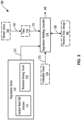
- FIG. 3 shows, in block diagram form, an example digital twin system 300 for monitoring degradation in a bond pad to bond ball interface such as the interface 120 shown in FIG. 1 .
- the digital twin system 300 includes a degradation sensor 310 and a degradation modelling controller 330.
- the digital twin system 300 can also include one or more of the optional embedded sensor 350, remote sensor 360, filter 370, and historical data storage 380, denoted with dashed-line borders.
- the degradation modelling controller 330 can be any appropriate digital logic circuit, such as one or more central processing units, digital signal processors, application specific integrated circuits, microcontrollers and the like.
- the degradation sensor 310 is described further herein with respect to FIGS. 4-5 and includes a stacked bond ball structure 315 and a resistance-sensing circuit 320.
- the stacked bond ball structure 315 is a first bond ball on a bond pad and a second bond ball positioned on the first bond ball.
- the resistance-sensing circuit 320 is configured to measure a resistance of the interface between the first bond ball and the bond pad in the stacked bond ball structure 315.
- the resistance-sensing circuit 320 is a four-terminal resistance-sensing circuit.
- the stacked bond ball structure 315 enables a four point electric resistance measurement, which may be more accurate than a two point resistance measurement enabled by a single bond ball because the contact resistance of the probes in the four-terminal resistance-sensing circuit are not measured.
- the resistance between the first and second bond balls may be sufficiently less than the resistance of the interface between the first bond ball and the bond pad such that the resistance of the interface between the first bond ball and the bond pad may be accurately determined.
- the output 325 from the degradation sensor 310 can be the measured resistance of the interface between the first bond ball and the bond pad in the stacked bond ball structure 315 or information from which the resistance of the interface can be determined, such as the measured voltage and current from a four-terminal resistance-sensing circuit.
- the degradation modelling controller 330 receives the output 325 from the degradation sensor 310 and determines an amount of degradation of the interface based on the output 325.
- the degradation modelling controller 330 may include a model for the relationship between degradation of the bond pad to bond ball interface and the resistance of the interface.
- the output 340 from the degradation modelling controller 330 is provided to other systems, which can adjust one or more operating parameters or perform an operation based on the output 340.
- the output 340 from the degradation modelling controller 330 is the determined amount of degradation of the interface.
- the degradation modelling controller 330 estimates a "remaining useful life" of the interface, which can represent a predicted amount of time before the interface degrades below a threshold of performance.
- the controller receives multiple outputs 325 from the degradation sensor 310 over time and determines the "remaining useful life" of the interface based on the historical outputs 325 as well as the current output 325. For example, the degradation modelling controller 330 may update the model of the relationship between the degradation of the interface and the resistance of the interface based on the historical outputs over time.
- the digital twin system 300 also includes the optional embedded sensor 350, such as a temperature sensor, a humidity sensor, or the like.
- the model for the relationship between degradation of the bond pad to bond ball interface and the resistance of the interface may further model the influence of temperature, humidity, and the like.
- the output 355 from the embedded sensor 350 is provided to the degradation modelling controller 330, which can then determine the amount of degradation of the interface based on both the output 325 from the degradation sensor 310 and the output 355 from the optional embedded sensor 350.
- the digital twin system 300 also includes the remote sensor 360, such as a temperature sensor, a humidity sensor, or the like.
- the remote sensor 360 can be a shared temperature sensor for the digital twin system 300 and other systems, such as a battery management system.
- the types of sensors 350 and 360 can be chosen to complement each other.
- the remote sensor 360 can be the shared temperature sensor, and the embedded sensor 350 can be a humidity sensor.
- the remote sensor 360 outputs the remote sensor data 365.
- the remote sensor 360 outputs the remote sensor data 365 directly to the degradation modelling controller 330, which can then determine the amount of degradation of the interface based on both the output 325 from the degradation sensor 310 and the output 365 from the optional remote sensor 360.
- the remote sensor 360 outputs the remote sensor data 365 to the filter 370.
- the filter 370 applies a transfer function to the remote sensor data 365 to convert the remote data values to approximate local data values 375 at the degradation sensor 310.
- the remote sensor 360 is a temperature sensor
- the filter 370 converts the remote temperature data 365 to approximate temperature values 375 at the degradation sensor 310.
- the output 375 from the filter 370 is provided to the degradation modelling controller 330, which can then determine the amount of degradation of the interface based on both the output 325 from the degradation sensor 310 and the output 375 from the optional filter 370.
- the digital twin system 300 also includes the optional historical data storage 380, which may be used to store instructions and/or data received from the degradation modelling controller 330 over bus 385.
- the historical data storage 380 may be any appropriate non-transitory computer readable storage medium, such as one or more non-volatile memory devices.
- the degradation modelling controller 330 can store historical data such as historical values of output 340 from the degradation modelling controller 330, historical values of output 325 from degradation sensor 310, historical values of output 355 from optional embedded sensor 350, historical values of output 365 from optional remote sensor 360, and historical values of output 375 from optional filter 370.
- the degradation modelling controller 330 may update the model of the degradation of the interface based on the historical data in storage 380 and further determine the amount of degradation of the interface based on the historical data.
- the embedded sensor 350 is a humidity sensor
- the remote sensor 360 is a temperature sensor.
- storage 380 can also store historic use data for the system.
- the digital twin system 300 can be included in an automotive driving assistance system on a vehicle, and the historical data storage 380 can store information about the vehicle's usage, such as the total number of miles it has been driven, how often it is driven, what conditions it is driven in, what conditions it is parked in, and the like.
- the degradation modelling controller 330 may update the model of the degradation of the interface based on the historical use data in storage 380 and further determine the amount of degradation of the interface based on the historical use data in storage 380.
- FIG. 4 shows a cross section of an example integrated circuit (IC) 400 with a stacked bond ball structure for the degradation sensor 310 in the digital twin system 300 shown in FIG. 3 .
- the example IC 400 includes a substrate 410, bond pads 420A-C, electrical connection 430 between the bond pads 420A-C, bond balls 440A-C, stacked bond ball 460, and wire bonds 470A-B.
- the bond ball 440A is positioned on bond pad 420A
- the bond ball 440B is positioned on bond pad 420B
- the bond ball 440C is positioned on bond pad 420C.
- the stacked bond ball 460 is positioned on the bond ball 440B, and the bond ball 440B and the stacked bond ball 460 form a stacked bond ball structure.
- the wire bond 470A couples the bond ball 440A to the bond ball 440B, and the wire bond 470B couples the stacked bond ball 460 to the bond ball 440C.
- the interface 450 between the bond ball 440B and the bond pad 420B can experience degradation over time, just as the other bond pad to bond ball interfaces on the device experience, such that the interface 450 can be incorporated into a digital twin system such as digital twin system 300 shown in FIG. 3 .
- the resistance of the interface 450 can be measured to model the degradation experienced by the other bond pad to bond ball interfaces and predict an amount of remaining useful life for the bond pad to bond ball interfaces.
- a four-terminal resistance-sensing system can be used to measure a voltage V 480 using the bond balls 440A and 440B and wire bond 470A and a current I 490 using the bond ball 440C and the stacked bond ball 460. Based on the measured voltage V 480 and measured current I 490, the resistance of the interface 450 can be determined.
- the current I 490 is shown through the stacked bond ball 460 and the bond ball 440C, and the voltage V 480 is shown across the bond balls 440A and 440B, but in other implementations, the current I 490 may be measured through the bond balls 440A and 440B, and the voltage 480 may be measured across the stacked bond ball 460 and the bond ball 440C.
- the stacked bond ball structure comprising the bond ball 440B and the stacked bond ball 460 enables a four point electric resistance measurement, which may be more accurate than a two point resistance measurement enabled by the bond ball 440B alone because the contact resistance of the probes in the four-terminal resistance-sensing circuit are not measured.
- FIG. 5 shows a cross section of another example IC 500 with two stacked bond ball structures for the degradation sensor 310 in the digital twin system 300 shown in FIG. 3 .
- the example IC 500 is similar to the example IC 400 shown in FIG. 4 but includes two stacked bond balls 560A and 560B, only two bond pads 520A and 520B, only two bond balls 540A and 540B, and only one wire bond 570.
- the bond ball 540A is positioned on bond pad 520A
- the bond ball 540B is positioned on bond pad 520B.
- the stacked bond ball 560A is positioned on the bond ball 540A and together form a stacked bond ball structure.
- the stacked bond ball 560B is positioned on the bond ball 540B and together form a stacked bond ball structure.
- the wire bond 570 couples the stacked bond ball 560A to the stacked bond ball 560B.
- the resistance of two interfaces can be monitored: the interface 550A between the bond ball 540A and the bond pad 520A and the interface 550B between the bond ball 540B and the bond pad 520B.
- the resistance of the interfaces 550A and 550B can be measured to model the degradation experienced by the other bond pad to bond ball interfaces and predict an amount of remaining useful life for the bond pad to bond ball interfaces.
- a four-terminal resistance-sensing system can be used to measure a voltage V 580 using the bond balls 540A and 540B and a current I 590 using the stacked bond balls 560A and 560B and wire bond 570. Based on the measured voltage V 580 and measured current I 590, the resistance of the interfaces 550A and 550B can be determined.
- the current I 590 is shown through the stacked bond balls 560A and 560B, and the voltage V 580 is shown across the bond balls 540A and 540B, but in other implementations, the current I 590 may be measured through the bond balls 540A and 540B, and the voltage V 580 may be measured across the stacked bond balls 560A and 560B.
- the stacked bond ball structures enable a four point electric resistance measurement, which may be more accurate than a two point resistance measurement enabled by the bond balls 540A and 540B alone because the contact resistance of the probes in the four-terminal resistance-sensing circuit are not measured.
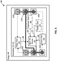
- FIG. 6 shows an example digital twin system 600 for monitoring degradation in a bond pad to bond ball interface encapsulated in a single semiconductor die 610 and package 690.
- the digital twin system 600A includes the semiconductor die 610, the stacked bond ball structures 615A and 615B, and the package 690.
- the semiconductor die 610 includes the digital twin processor 620, the voltage sensing pads 625A and 625B, the voltage sensor 630, the current sensing pads 645A and 645B, and the current sensor 650.
- the semiconductor die 610 also includes the optional humidity sensor 670, the temperature sensor 680, or both.
- the voltage sensor 630 measures a voltage across voltage sensing pads 625A and 625B and provides the measured voltage 640 to the digital twin processor 620.
- the current sensor 650 measures a current from current sensing pad 645A to current sensing pad 645B and provides the measured current 660 to the digital twin processor 620.
- the digital twin processor 620 can perform the operations of degradation modelling controller 330 shown in FIG. 3 and determine an amount of degradation of the interfaces between the first bond balls in the stacked bond ball structures 615A and 615B and the corresponding bond pads.
- the measured humidity 675 is provided to the digital twin processor 620 as well, and the digital twin processor 620 further determines the amount of degradation of the interfaces based on the measured humidity 675.
- the measured temperature 685 is provided to the digital twin processor 620 as well, and the digital twin processor 620 further determines the amount of degradation of the interfaces based on the measured temperature 685.
- the digital twin system 600 shown in FIG. 6 encapsulates the digital twin processor 620, the stacked bond ball structures 615A and 615B, and the optional sensors 670 and 680 in a single semiconductor die 610 and a single package 690.
- the digital twin processor 620, the stacked bond ball structures 615A and 615B, and the optional sensors 670 and 680 can be separated between multiple semiconductor dies 610 and encapsulated in one or more packages 690.
- the digital twin system 700 includes four semiconductor dies 710A, 710B, 710C, and 710D encapsulated in a single package 790.
- the semiconductor die 710A includes the stacked bond ball structures 715A and 715B, the voltage sensing pads 725A and 725B, the voltage sensor 730, the current sensing pads 745A and 745B, and the current sensor 750.
- the semiconductor die 710B includes the digital twin processor 720
- the semiconductor die 710C includes the humidity sensor 770
- the semiconductor die 710D includes the temperature sensor 780.
- the semiconductor dies 710A-D are encapsulated in a single package 790.
- the semiconductor dies 710A-D are encapsulated in multiple packages 790.
- the digital twin system 800 includes four semiconductor dies 810A-D and four packages 890A-D.
- the stacked bond ball structures 815A and 815B are coupled to output pins 865A-D.
- the stacked bond ball structure 815A is coupled to pin 865A for a voltage sensing output 825A and to pin 865C for a current sensing output 845A.
- the stacked bond ball structure 815B is coupled to pin 865B for a voltage sensing output 825B and to pin 865D for a current sensing output 845B.
- the semiconductor die 810B includes the digital twin processor 820, the voltage sensor 830, and the current sensor 850.
- the voltage sensor 830 is coupled to pins 865A and 865B in package 890A
- the current sensor 850 is coupled to pins 865C and 865D in package 890A.
- the semiconductor die 810B is encapsulated in package 890B.
- the semiconductor die 810C includes the optional humidity sensor 870 and is encapsulated in package 890C.
- the semiconductor die 810D includes the optional temperature sensor 880 and is encapsulated in package 890D.
- the combinations of semiconductor dies and packages of digital twin systems 600, 700, and 800 shown in FIGS. 6 , 7 , and 8 are examples and can be combined or modified based on the particular implementation.
- digital twin systems 600, 700, and 800 shown in FIGS. 6 , 7 , and 8 illustrate the example implementation with two stacked bond ball structures described in FIG. 5 , but in other implementations, the digital twin systems 600, 700, and 800 may be implemented with the single stacked bond ball structure described in FIG. 4 .
- Couple may cover connections, communications, or signal paths that enable a functional relationship consistent with this description, including intermediate or intervening components that do not alter the functional relationship.
- a device that is "configured to" perform a task or function may be configured by programming or hardwiring, for example, at a time of manufacturing by a manufacturer and/or may be configurable or reconfigurable by a user after manufacturing. The configuring may be done through firmware and/or software, construction and/or layout of hardware components and connections, or any combination thereof.
- node "pin”, and “lead” are used interchangeably.
- a circuit or device described herein as including certain components may be adapted to be coupled to those components instead, to form the described circuitry or device.
Landscapes
- Engineering & Computer Science (AREA)
- General Engineering & Computer Science (AREA)
- Physics & Mathematics (AREA)
- General Physics & Mathematics (AREA)
- Computer Hardware Design (AREA)
- Microelectronics & Electronic Packaging (AREA)
- Environmental & Geological Engineering (AREA)
- Investigating Or Analyzing Materials By The Use Of Electric Means (AREA)
- Testing Or Measuring Of Semiconductors Or The Like (AREA)
Abstract
Description
- Integrated circuits are used in safety-critical systems, such as driver assistance systems and medical devices. As a result, monitoring the wear and degradation of components in safety-critical systems may be important to maintain operational integrity and reliability.
- A device comprises a substrate and a stacked bond ball structure. The substrate comprises a bond pad, and the stacked bond ball structure comprises a first bond ball in contact with the bond pad and a second bond ball positioned on the first bond ball. The stacked bond ball structure is configured to be coupled to a resistance-sensing circuit such that a resistance of an interface between the first bond ball and the bond pad can be measured to determine an amount of degradation of the interface between the first bond ball and the bond pad. In some implementations, the device further comprises a controller configured to obtain a measured resistance of the interface between the first bond ball and the bond pad from the resistance-sensing circuit and determine the amount of degradation of the interface based at least in part on the measured resistance of the interface.
- In some implementations, the bond pad is a first bond pad, and the substrate further comprises second and third bond pads electrically connected to the first bond pad. The device further comprises a third bond ball in contact with the second bond pad, a fourth bond ball in contact with the third bond pad, and the resistance-sensing circuit. The resistance-sensing circuit comprises a current sensor configured to measure a current between the stacked bond ball structure and the third bond ball and a voltage sensor configured to measure a voltage between the stacked bond ball structure and the fourth bond ball. The controller is configured to determine the measured resistance of the interface between the first bond ball and the first bond pad based on a measured current from the current sensor and a measured voltage from the voltage sensor.
- In some implementations, the device further comprises a first semiconductor die and a second semiconductor die. The first semiconductor die comprises the substrate, the stacked bond ball structure, and the third and fourth bond balls. The second semiconductor die comprises the controller. In some implementations, the resistance-sensing circuit is comprised on one of the first semiconductor die, the second semiconductor die, and a third semiconductor die.
- The bond pad is a first bond pad, and the stacked bond ball structure is a first stacked bond ball structure, in some implementations. The substrate further comprises a second bond pad electrically connected to the first bond pad. The device further comprises a second stacked bond ball structure and the resistance-sensing circuit. The second stacked bond ball comprises a third bond ball in contact with the second bond pad and a fourth bond ball positioned on the third bond ball. The resistance-sensing circuit comprises a current sensor configured to measure a current between the first bond ball and the third bond ball and a voltage sensor configured to measure a voltage between the second bond ball and the fourth bond ball. The controller is further configured to determine the measured resistance of the interface between the first bond ball and the first bond pad based on a measured current from the current sensor and a measured voltage from the voltage sensor.
- In some implementations, a first semiconductor die comprises the substrate and the first and second stacked bond ball structures, and a second semiconductor die comprises the controller. The resistance sensing circuit is comprised on one of the first semiconductor die, the second semiconductor die, and a third semiconductor die. In some implementations, the controller is further configured to obtain sensor data from a sensor and to determine the amount of degradation of the interface further based on the sensor data. The sensor data comprises at least one of temperature data, humidity data, and contamination data.
- An apparatus comprises a substrate, an embedded degradation sensor, and a controller. The substrate comprises a bond pad, and the embedded degradation sensor is coupled to the bond pad. The embedded degradation sensor comprises a first bond ball in contact with the first bond pad, a second bond ball positioned on the first bond ball, and a resistance-sensing system configured to measure a resistance of an interface between the first bond ball and the bond pad. The controller is configured to determine an amount of degradation of the interface between the first bond ball and the bond pad based at least in part on the resistance of the interface. In some implementations, the controller is further configured to determine a remaining useful life of wire bonds in the apparatus based on the amount of degradation of the interface.
- In some implementations, the apparatus further comprises a sensor, and the controller is further configured to obtain sensor data from the sensor and determine the amount of degradation of the interface further based on the sensor data. The sensor is one of a temperature sensor, a humidity sensor, and a contamination sensor, in some implementations. The apparatus further comprises, in some implementations, a memory configured to store historical sensor data, and the controller is configured to determine the amount of degradation of the interface further based on the historical sensor data. The apparatus further comprises, in some implementations, a memory configured to store historical resistance data, and the controller is configured to determine the amount of degradation of the interface further based on the historical resistance data.
- A method comprises measuring a resistance of an interface between a stacked bond ball structure and a bond pad and estimating, based at least in part on the measured resistance of the interface, a remaining useful life of wire bonds in a device comprising the stacked bond ball structure. In some implementations, measuring the resistance of the interface comprises measuring a voltage across the interface and measuring a current through the interface. In some implementations, the method further comprises obtaining at least one of temperature data, humidity data, and contamination data for the stacked bond ball structure and determining the remaining useful life further based on the at least one of the temperature data, the humidity data, and the contamination data. In some implementations, the method further comprises storing, in a memory, the measured resistance of the interface; measuring, at a later time, the resistance of the interface to obtain an updated measured resistance; and estimating, based at least in part on the updated measured resistance and the stored measured resistance, an updated remaining useful life of wire bonds in the device.
- The present invention may be better understood, and its numerous objects, features, and advantages made apparent to those skilled in the art by referencing the accompanying drawings.
-
FIG. 1 shows a planar view of a bond pad to bond ball interface. -
FIG. 2 shows a planar view of a degraded bond pad to bond ball interface after etching of the ball bond. -
FIG. 3 shows, in block diagram form, an example digital twin system for monitoring degradation in a bond pad to bond ball interface. -
FIG. 4 shows a cross section of an example integrated circuit with a stacked bond ball structure for the degradation sensor in the digital twin system shown inFIG. 3 . -
FIG. 5 shows a cross section of another example integrated circuit with stacked bond ball structures for the degradation sensor in the digital twin system shown inFIG. 3 . -
FIG. 6 shows an example digital twin system for monitoring degradation in a bond pad to bond ball interface incorporated into a single integrated circuit and package. -
FIG. 7 shows an example digital twin system for monitoring degradation in a bond pad to bond ball interface incorporated into multiple integrated circuits in a single package. -
FIG. 8 shows an example digital twin system for monitoring degradation in a bond pad to bond ball interface incorporated into multiple integrated circuits in multiple packages. - The use of the same reference symbols in different drawings indicates identical items unless otherwise noted. The Figures are not necessarily drawn to scale.
- As disclosed herein, an apparatus includes a substrate comprising a bond pad, an embedded degradation sensor coupled to the bond pad, and a controller. The embedded degradation sensor includes a first bond ball in contact with the bond pad, a second bond ball positioned on the first bond ball, and a resistance-sensing system configured to measure a resistance of an interface between the first bond ball and the bond pad. The controller is configured to determine an amount of degradation of the interface between the first bond ball and the bond pad based at least in part on the resistance of the interface. The apparatus can act as a digital twin and allow the system to predict a remaining useful life of wire bonds in the apparatus.
-
FIG. 1 shows aplanar view 100 of a bond pad to bond ball interface. Thebond pad 110 shows an intact,undegraded interface 120 between thebond pad 110 and the bond ball. However, mechanisms such as corrosion and Kirkendall voids can degrade the interface between thebond pad 110 and the bond ball. For example, thebond pad 110 can be aluminum, and the bond ball can be copper, which is susceptible to corrosion. Theplanar view 200 inFIG. 2 shows a degraded bond pad to bond ball interface. Thebond pad 210 shows a small,intact area 230 of the interface between thebond pad 210 and the bond ball, and acorrosion front 240 between theintact area 230 and thedegraded area 220. The degradation of the bond pad to bond ball interface may change the characteristics of the interface, for example the resistance of the interface. -
FIG. 3 shows, in block diagram form, an exampledigital twin system 300 for monitoring degradation in a bond pad to bond ball interface such as theinterface 120 shown inFIG. 1 . Thedigital twin system 300 includes adegradation sensor 310 and adegradation modelling controller 330. Thedigital twin system 300 can also include one or more of the optional embeddedsensor 350,remote sensor 360,filter 370, andhistorical data storage 380, denoted with dashed-line borders. Thedegradation modelling controller 330 can be any appropriate digital logic circuit, such as one or more central processing units, digital signal processors, application specific integrated circuits, microcontrollers and the like. - The
degradation sensor 310 is described further herein with respect toFIGS. 4-5 and includes a stackedbond ball structure 315 and a resistance-sensing circuit 320. The stackedbond ball structure 315 is a first bond ball on a bond pad and a second bond ball positioned on the first bond ball. The resistance-sensing circuit 320 is configured to measure a resistance of the interface between the first bond ball and the bond pad in the stackedbond ball structure 315. In some implementations, the resistance-sensing circuit 320 is a four-terminal resistance-sensing circuit. The stackedbond ball structure 315 enables a four point electric resistance measurement, which may be more accurate than a two point resistance measurement enabled by a single bond ball because the contact resistance of the probes in the four-terminal resistance-sensing circuit are not measured. In addition, the resistance between the first and second bond balls may be sufficiently less than the resistance of the interface between the first bond ball and the bond pad such that the resistance of the interface between the first bond ball and the bond pad may be accurately determined. - The
output 325 from thedegradation sensor 310 can be the measured resistance of the interface between the first bond ball and the bond pad in the stackedbond ball structure 315 or information from which the resistance of the interface can be determined, such as the measured voltage and current from a four-terminal resistance-sensing circuit. Thedegradation modelling controller 330 receives theoutput 325 from thedegradation sensor 310 and determines an amount of degradation of the interface based on theoutput 325. For example, thedegradation modelling controller 330 may include a model for the relationship between degradation of the bond pad to bond ball interface and the resistance of the interface. Theoutput 340 from thedegradation modelling controller 330 is provided to other systems, which can adjust one or more operating parameters or perform an operation based on theoutput 340. - In some implementations, the
output 340 from thedegradation modelling controller 330 is the determined amount of degradation of the interface. In other implementations, thedegradation modelling controller 330 estimates a "remaining useful life" of the interface, which can represent a predicted amount of time before the interface degrades below a threshold of performance. In some implementations, the controller receivesmultiple outputs 325 from thedegradation sensor 310 over time and determines the "remaining useful life" of the interface based on thehistorical outputs 325 as well as thecurrent output 325. For example, thedegradation modelling controller 330 may update the model of the relationship between the degradation of the interface and the resistance of the interface based on the historical outputs over time. - In some implementations, the
digital twin system 300 also includes the optional embeddedsensor 350, such as a temperature sensor, a humidity sensor, or the like. The model for the relationship between degradation of the bond pad to bond ball interface and the resistance of the interface may further model the influence of temperature, humidity, and the like. Theoutput 355 from the embeddedsensor 350 is provided to thedegradation modelling controller 330, which can then determine the amount of degradation of the interface based on both theoutput 325 from thedegradation sensor 310 and theoutput 355 from the optional embeddedsensor 350. - In some implementations, the
digital twin system 300 also includes theremote sensor 360, such as a temperature sensor, a humidity sensor, or the like. For example, theremote sensor 360 can be a shared temperature sensor for thedigital twin system 300 and other systems, such as a battery management system. In implementations including both embeddedsensor 350 andremote sensor 360, the types ofsensors remote sensor 360 can be the shared temperature sensor, and the embeddedsensor 350 can be a humidity sensor. Theremote sensor 360 outputs theremote sensor data 365. In some implementations, theremote sensor 360 outputs theremote sensor data 365 directly to thedegradation modelling controller 330, which can then determine the amount of degradation of the interface based on both theoutput 325 from thedegradation sensor 310 and theoutput 365 from the optionalremote sensor 360. - In other implementations, the
remote sensor 360 outputs theremote sensor data 365 to thefilter 370. Thefilter 370 applies a transfer function to theremote sensor data 365 to convert the remote data values to approximatelocal data values 375 at thedegradation sensor 310. For example, theremote sensor 360 is a temperature sensor, and thefilter 370 converts theremote temperature data 365 toapproximate temperature values 375 at thedegradation sensor 310. Theoutput 375 from thefilter 370 is provided to thedegradation modelling controller 330, which can then determine the amount of degradation of the interface based on both theoutput 325 from thedegradation sensor 310 and theoutput 375 from theoptional filter 370. - In some implementations, the
digital twin system 300 also includes the optionalhistorical data storage 380, which may be used to store instructions and/or data received from thedegradation modelling controller 330 overbus 385. Thehistorical data storage 380 may be any appropriate non-transitory computer readable storage medium, such as one or more non-volatile memory devices. Thedegradation modelling controller 330 can store historical data such as historical values ofoutput 340 from thedegradation modelling controller 330, historical values ofoutput 325 fromdegradation sensor 310, historical values ofoutput 355 from optional embeddedsensor 350, historical values ofoutput 365 from optionalremote sensor 360, and historical values ofoutput 375 fromoptional filter 370. For example, thedegradation modelling controller 330 may update the model of the degradation of the interface based on the historical data instorage 380 and further determine the amount of degradation of the interface based on the historical data. For example, the embeddedsensor 350 is a humidity sensor, and theremote sensor 360 is a temperature sensor. Thedegradation modelling controller 330 can determine the degradation D of the interface, which can be represented as:
humidity sensor 350, Ea represents an activation energy of a component material of the interface, kB represents the Boltzmann constant, T represents a temperature measured by theremote temperature sensor 360, and t represents time. - In addition to historical sensor data,
storage 380 can also store historic use data for the system. For example, thedigital twin system 300 can be included in an automotive driving assistance system on a vehicle, and thehistorical data storage 380 can store information about the vehicle's usage, such as the total number of miles it has been driven, how often it is driven, what conditions it is driven in, what conditions it is parked in, and the like. Then, thedegradation modelling controller 330 may update the model of the degradation of the interface based on the historical use data instorage 380 and further determine the amount of degradation of the interface based on the historical use data instorage 380. -
FIG. 4 shows a cross section of an example integrated circuit (IC) 400 with a stacked bond ball structure for thedegradation sensor 310 in thedigital twin system 300 shown inFIG. 3 . Theexample IC 400 includes asubstrate 410,bond pads 420A-C,electrical connection 430 between thebond pads 420A-C,bond balls 440A-C, stackedbond ball 460, andwire bonds 470A-B. Thebond ball 440A is positioned onbond pad 420A, thebond ball 440B is positioned onbond pad 420B, and thebond ball 440C is positioned onbond pad 420C. The stackedbond ball 460 is positioned on thebond ball 440B, and thebond ball 440B and the stackedbond ball 460 form a stacked bond ball structure. Thewire bond 470A couples thebond ball 440A to thebond ball 440B, and thewire bond 470B couples the stackedbond ball 460 to thebond ball 440C. - The
interface 450 between thebond ball 440B and thebond pad 420B can experience degradation over time, just as the other bond pad to bond ball interfaces on the device experience, such that theinterface 450 can be incorporated into a digital twin system such asdigital twin system 300 shown inFIG. 3 . The resistance of theinterface 450 can be measured to model the degradation experienced by the other bond pad to bond ball interfaces and predict an amount of remaining useful life for the bond pad to bond ball interfaces. For example, a four-terminal resistance-sensing system can be used to measure avoltage V 480 using thebond balls wire bond 470A and acurrent I 490 using thebond ball 440C and the stackedbond ball 460. Based on the measuredvoltage V 480 and measuredcurrent I 490, the resistance of theinterface 450 can be determined. - In this example, the
current I 490 is shown through the stackedbond ball 460 and thebond ball 440C, and thevoltage V 480 is shown across thebond balls bond balls voltage 480 may be measured across the stackedbond ball 460 and thebond ball 440C. The stacked bond ball structure comprising thebond ball 440B and the stackedbond ball 460 enables a four point electric resistance measurement, which may be more accurate than a two point resistance measurement enabled by thebond ball 440B alone because the contact resistance of the probes in the four-terminal resistance-sensing circuit are not measured. -
FIG. 5 shows a cross section of anotherexample IC 500 with two stacked bond ball structures for thedegradation sensor 310 in thedigital twin system 300 shown inFIG. 3 . Theexample IC 500 is similar to theexample IC 400 shown inFIG. 4 but includes twostacked bond balls bond pads bond balls wire bond 570. Thebond ball 540A is positioned onbond pad 520A, and thebond ball 540B is positioned onbond pad 520B. The stackedbond ball 560A is positioned on thebond ball 540A and together form a stacked bond ball structure. Similarly, the stackedbond ball 560B is positioned on thebond ball 540B and together form a stacked bond ball structure. Thewire bond 570 couples the stackedbond ball 560A to the stackedbond ball 560B. - In the
example IC 500, the resistance of two interfaces can be monitored: theinterface 550A between thebond ball 540A and thebond pad 520A and theinterface 550B between thebond ball 540B and thebond pad 520B. The resistance of theinterfaces voltage V 580 using thebond balls current I 590 using the stackedbond balls wire bond 570. Based on the measuredvoltage V 580 and measuredcurrent I 590, the resistance of theinterfaces - In this example, the
current I 590 is shown through the stackedbond balls voltage V 580 is shown across thebond balls bond balls voltage V 580 may be measured across the stackedbond balls bond balls -
FIG. 6 shows an exampledigital twin system 600 for monitoring degradation in a bond pad to bond ball interface encapsulated in asingle semiconductor die 610 andpackage 690. The digital twin system 600A includes the semiconductor die 610, the stackedbond ball structures package 690. The semiconductor die 610 includes the digitaltwin processor 620, thevoltage sensing pads voltage sensor 630, thecurrent sensing pads current sensor 650. In some implementations, the semiconductor die 610 also includes theoptional humidity sensor 670, thetemperature sensor 680, or both. Thevoltage sensor 630 measures a voltage acrossvoltage sensing pads voltage 640 to the digitaltwin processor 620. Thecurrent sensor 650 measures a current fromcurrent sensing pad 645A tocurrent sensing pad 645B and provides the measured current 660 to the digitaltwin processor 620. - The digital
twin processor 620 can perform the operations ofdegradation modelling controller 330 shown inFIG. 3 and determine an amount of degradation of the interfaces between the first bond balls in the stackedbond ball structures optional humidity sensor 670, the measuredhumidity 675 is provided to the digitaltwin processor 620 as well, and the digitaltwin processor 620 further determines the amount of degradation of the interfaces based on the measuredhumidity 675. In implementations including theoptional temperature sensor 680, the measuredtemperature 685 is provided to the digitaltwin processor 620 as well, and the digitaltwin processor 620 further determines the amount of degradation of the interfaces based on the measuredtemperature 685. - The
digital twin system 600 shown inFIG. 6 encapsulates the digitaltwin processor 620, the stackedbond ball structures optional sensors single semiconductor die 610 and asingle package 690. In other embodiments, the digitaltwin processor 620, the stackedbond ball structures optional sensors more packages 690. For example, inFIG. 7 , thedigital twin system 700 includes four semiconductor dies 710A, 710B, 710C, and 710D encapsulated in asingle package 790. The semiconductor die 710A includes the stackedbond ball structures voltage sensing pads voltage sensor 730, thecurrent sensing pads twin processor 720, the semiconductor die 710C includes thehumidity sensor 770, and the semiconductor die 710D includes thetemperature sensor 780. The semiconductor dies 710A-D are encapsulated in asingle package 790. - In other embodiments, the semiconductor dies 710A-D are encapsulated in
multiple packages 790. For example, inFIG. 8 , thedigital twin system 800 includes four semiconductor dies 810A-D and fourpackages 890A-D. On semiconductor die 810A, the stackedbond ball structures output pins 865A-D. The stackedbond ball structure 815A is coupled to pin 865A for avoltage sensing output 825A and to pin 865C for acurrent sensing output 845A. The stackedbond ball structure 815B is coupled to pin 865B for avoltage sensing output 825B and to pin 865D for acurrent sensing output 845B. - The semiconductor die 810B includes the digital
twin processor 820, thevoltage sensor 830, and thecurrent sensor 850. Thevoltage sensor 830 is coupled topins package 890A, and thecurrent sensor 850 is coupled topins package 890A. The semiconductor die 810B is encapsulated inpackage 890B. The semiconductor die 810C includes theoptional humidity sensor 870 and is encapsulated in package 890C. The semiconductor die 810D includes theoptional temperature sensor 880 and is encapsulated inpackage 890D. The combinations of semiconductor dies and packages of digitaltwin systems FIGS. 6 ,7 , and8 are examples and can be combined or modified based on the particular implementation. In addition, the digitaltwin systems FIGS. 6 ,7 , and8 illustrate the example implementation with two stacked bond ball structures described inFIG. 5 , but in other implementations, the digitaltwin systems FIG. 4 . - Features specifically shown or described with respect to one embodiment set forth herein may be implemented in other embodiments set forth herein.
- In this description, the term "couple" may cover connections, communications, or signal paths that enable a functional relationship consistent with this description, including intermediate or intervening components that do not alter the functional relationship. A device that is "configured to" perform a task or function may be configured by programming or hardwiring, for example, at a time of manufacturing by a manufacturer and/or may be configurable or reconfigurable by a user after manufacturing. The configuring may be done through firmware and/or software, construction and/or layout of hardware components and connections, or any combination thereof. As used herein, "node", "pin", and "lead" are used interchangeably. A circuit or device described herein as including certain components may be adapted to be coupled to those components instead, to form the described circuitry or device.
- While particular embodiments of the present invention have been shown and described, it will be recognized to those skilled in the art that, based upon the teachings herein, further changes and modifications may be made without departing from the invention, as defined by the appended claims.
Claims (14)
- A device, comprising:a substrate comprising a bond pad; anda stacked bond ball structure comprising a first bond ball in contact with the bond pad and a second bond ball positioned on the first bond ball, wherein the stacked bond ball structure is configured to be coupled to a resistance-sensing circuit such that a resistance of an interface between the first bond ball and the bond pad can be measured to determine an amount of degradation of the interface between the first bond ball and the bond pad.
- The device of claim 1, further comprising a controller configured to:obtain a measured resistance of the interface between the first bond ball and the bond pad from the resistance-sensing circuit; anddetermine the amount of degradation of the interface between the first bond ball and the bond pad based at least in part on the measured resistance of the interface.
- The device of claim 2, wherein:the bond pad is a first bond pad;the substrate further comprises a second bond pad and a third bond pad, wherein the first, second, and third bond pads are electrically connected;the device further comprises:a third bond ball in contact with the second bond pad;a fourth bond ball in contact with the third bond pad; andthe resistance-sensing circuit, comprising:a current sensor for measuring a current between the stacked bond ball structure and the third bond ball; anda voltage sensor for measuring a voltage between the stacked bond ball structure and the fourth bond ball; andthe controller is configured to determine the measured resistance of the interface between the first bond ball and the first bond pad based on a measured current from the current sensor and a measured voltage from the voltage sensor.
- The device of claim 3, further comprising:a first semiconductor die having the substrate, the stacked bond ball structure, and the third and fourth bond balls; anda second semiconductor die having the controller.
- The device of claim 4, wherein the resistance-sensing circuit is comprised on one of the first semiconductor die, the second semiconductor die, and a third semiconductor die.
- The device of claim 2, wherein:the bond pad is a first bond pad;the stacked bond ball structure is a first stacked bond ball structure;the substrate further comprises a second bond pad electrically connected to the first bond pad;the device further comprises:a second stacked bond ball structure comprising a third bond ball in contact with the second bond pad and a fourth bond ball positioned on the third bond ball; andthe resistance-sensing circuit, comprising:
a current sensor for measuring a current between the first bond ball and the third bond ball; anda voltage sensor for measuring a voltage between the second bond ball and the fourth bond ball; andthe controller is further configured to determine the measured resistance of the interface between the first bond ball and the first bond pad based on a measured current from the current sensor and a measured voltage from the voltage sensor. - The device of claim 6, further comprising:a first semiconductor die having the substrate and the first and second stacked bond ball structures; anda second semiconductor die having the controller.
- The device of claim 7, wherein the resistance-sensing circuit is comprised on one of the first semiconductor die, the second semiconductor die, and a third semiconductor die.
- The device of any of claims 2 to 8, wherein the controller is further configured to obtain sensor data from a further sensor, and wherein the controller is configured to determine the amount of degradation of the interface further based on the sensor data.
- The device of claim 9, wherein the sensor data comprises at least one of temperature data, humidity data, and contamination data.
- A method, comprising:measuring a resistance of an interface between a stacked bond ball structure and a bond pad; andestimating, based at least in part on the measured resistance of the interface, a remaining useful life of wire bonds in a device comprising the stacked bond ball structure.
- The method of claim 11, wherein measuring the resistance of the interface comprises:measuring a voltage across the interface; andmeasuring a current through the interface.
- The method of claim 11 or 12, further comprising:obtaining at least one of temperature data, humidity data, and contamination data for the stacked bond ball structure; anddetermining the remaining useful life further based on the at least one of the temperature data, the humidity data, and the contamination data.
- The method of any of claims 11 to 13, further comprising:storing, in a memory, the measured resistance of the interface;measuring, at a later time, the resistance of the interface to obtain an updated measured resistance; andestimating, based at least in part on the updated measured resistance and the stored measured resistance, an updated remaining useful life of wire bonds in the device.
Applications Claiming Priority (1)
| Application Number | Priority Date | Filing Date | Title |
|---|---|---|---|
| US17/805,555 US12061228B2 (en) | 2022-06-06 | 2022-06-06 | Degradation monitor for bond wire to bond pad interfaces |
Publications (1)
| Publication Number | Publication Date |
|---|---|
| EP4290252A1 true EP4290252A1 (en) | 2023-12-13 |
Family
ID=88701002
Family Applications (1)
| Application Number | Title | Priority Date | Filing Date |
|---|---|---|---|
| EP23175632.1A Pending EP4290252A1 (en) | 2022-06-06 | 2023-05-26 | Degradation monitor for bond wire to bond pad interfaces |
Country Status (2)
| Country | Link |
|---|---|
| US (1) | US12061228B2 (en) |
| EP (1) | EP4290252A1 (en) |
Families Citing this family (1)
| Publication number | Priority date | Publication date | Assignee | Title |
|---|---|---|---|---|
| US20250014950A1 (en) * | 2023-07-03 | 2025-01-09 | Kla Corporation | Mini environment instrumented wafer |
Citations (8)
| Publication number | Priority date | Publication date | Assignee | Title |
|---|---|---|---|---|
| US6037795A (en) * | 1997-09-26 | 2000-03-14 | International Business Machines Corporation | Multiple device test layout |
| US20060194353A1 (en) * | 2005-02-28 | 2006-08-31 | Ridgetop Group, Inc. | Method and circuit for the detection of solder-joint failures in a digital electronic package |
| US20080088335A1 (en) * | 2005-06-23 | 2008-04-17 | Blanchet Jason E | Packaging reliability superchips |
| US20130087915A1 (en) * | 2011-10-10 | 2013-04-11 | Conexant Systems, Inc. | Copper Stud Bump Wafer Level Package |
| US20140091829A1 (en) * | 2012-09-28 | 2014-04-03 | Kabushiki Kaisha Toshiba | Semiconductor device, apparatus of estimating lifetime, method of estimating lifetime |
| US20190242940A1 (en) * | 2018-02-02 | 2019-08-08 | Texas Instruments Incorporated | Bondwire testing of ic using pin diode signatures |
| US20200200883A1 (en) * | 2018-12-19 | 2020-06-25 | Continental Automotive Systems, Inc. | Methods and systems for testing bonding of a sensor assembly |
| US20200210354A1 (en) * | 2018-12-30 | 2020-07-02 | Proteantecs Ltd. | Integrated circuit I/O integrity and degradation monitoring |
Family Cites Families (13)
| Publication number | Priority date | Publication date | Assignee | Title |
|---|---|---|---|---|
| US5654896A (en) * | 1994-10-31 | 1997-08-05 | Ixys Corp | Performance prediction method for semiconductor power modules and ICS |
| US5485095A (en) * | 1994-11-10 | 1996-01-16 | International Business Machines Corporation | Fabrication test circuit and method for signalling out-of-spec resistance in integrated circuit structure |
| US5751015A (en) * | 1995-11-17 | 1998-05-12 | Micron Technology, Inc. | Semiconductor reliability test chip |
| US7446419B1 (en) * | 2004-11-10 | 2008-11-04 | Bridge Semiconductor Corporation | Semiconductor chip assembly with welded metal pillar of stacked metal balls |
| US7825672B2 (en) | 2006-06-19 | 2010-11-02 | Mrl Industries, Inc. | High accuracy in-situ resistance measurements methods |
| US7693625B2 (en) | 2007-01-09 | 2010-04-06 | Gm Global Technology Operations, Inc. | State of health monitoring and reset methods and systems for on-board device driver integrated circuits |
| US7622737B2 (en) | 2007-07-11 | 2009-11-24 | International Business Machines Corporation | Test structures for electrically detecting back end of the line failures and methods of making and using the same |
| WO2009072052A1 (en) * | 2007-12-06 | 2009-06-11 | Nxp B.V. | Semiconductor device and wafer with a test structure and method for assessing adhesion of under-bump metallization |
| GB0818239D0 (en) | 2008-10-06 | 2008-11-12 | Omiino Ltd | System for internally monitoring an intergrated circuit |
| JP2014022652A (en) * | 2012-07-20 | 2014-02-03 | Elpida Memory Inc | Semiconductor device and test equipment therefor, and semiconductor device test method |
| US10026714B2 (en) | 2014-02-14 | 2018-07-17 | Nxp Usa, Inc. | Integrated circuit device |
| DE102017109266A1 (en) | 2017-04-28 | 2018-10-31 | Infineon Technologies Ag | Health monitoring of a circuit |
| US11099232B2 (en) * | 2019-02-01 | 2021-08-24 | Intel Corporation | On-die reliability monitor for integrated circuit |
-
2022
- 2022-06-06 US US17/805,555 patent/US12061228B2/en active Active
-
2023
- 2023-05-26 EP EP23175632.1A patent/EP4290252A1/en active Pending
Patent Citations (8)
| Publication number | Priority date | Publication date | Assignee | Title |
|---|---|---|---|---|
| US6037795A (en) * | 1997-09-26 | 2000-03-14 | International Business Machines Corporation | Multiple device test layout |
| US20060194353A1 (en) * | 2005-02-28 | 2006-08-31 | Ridgetop Group, Inc. | Method and circuit for the detection of solder-joint failures in a digital electronic package |
| US20080088335A1 (en) * | 2005-06-23 | 2008-04-17 | Blanchet Jason E | Packaging reliability superchips |
| US20130087915A1 (en) * | 2011-10-10 | 2013-04-11 | Conexant Systems, Inc. | Copper Stud Bump Wafer Level Package |
| US20140091829A1 (en) * | 2012-09-28 | 2014-04-03 | Kabushiki Kaisha Toshiba | Semiconductor device, apparatus of estimating lifetime, method of estimating lifetime |
| US20190242940A1 (en) * | 2018-02-02 | 2019-08-08 | Texas Instruments Incorporated | Bondwire testing of ic using pin diode signatures |
| US20200200883A1 (en) * | 2018-12-19 | 2020-06-25 | Continental Automotive Systems, Inc. | Methods and systems for testing bonding of a sensor assembly |
| US20200210354A1 (en) * | 2018-12-30 | 2020-07-02 | Proteantecs Ltd. | Integrated circuit I/O integrity and degradation monitoring |
Also Published As
| Publication number | Publication date |
|---|---|
| US20230393192A1 (en) | 2023-12-07 |
| US12061228B2 (en) | 2024-08-13 |
Similar Documents
| Publication | Publication Date | Title |
|---|---|---|
| CN101669037B (en) | Monitoring reliability of a digital system | |
| US6775624B2 (en) | Method and apparatus for estimating remaining life of a product | |
| US10502676B2 (en) | Disposable witness corrosion sensor | |
| US11177620B2 (en) | Laser failure early warning indicator | |
| CN101248365A (en) | System and method for estimating a state vector associated with a battery | |
| JP5216302B2 (en) | On-chip current measuring method and semiconductor integrated circuit | |
| JPH03177071A (en) | Integrated circuit thermal stress sensing device | |
| CN109477862B (en) | Vehicle control device | |
| US10352782B2 (en) | Thermal monitoring system in an integrated circuit die | |
| US12061228B2 (en) | Degradation monitor for bond wire to bond pad interfaces | |
| JP2018174885A (en) | Determination device, terminal device, determination system, program and determination method | |
| US20190361832A1 (en) | Bus system and detection method thereof | |
| EP3408667B1 (en) | Sensor signal processing device | |
| CN111044120A (en) | Battery-operated fill level measuring device with residual life determining device | |
| CN110347206A (en) | Car-mounted device, car-mounted device clock setting method and be stored with the storage medium of program | |
| JP2021524559A (en) | Vehicle braking system | |
| US8890556B2 (en) | Real-time on-chip EM performance monitoring | |
| CN105841734A (en) | Sensor system and method | |
| CN116205166A (en) | Circuits and techniques for modeling the remaining lifetime of semiconductor circuits | |
| JP2025532144A (en) | Urinary data recording device that senses filling state during acquisition cycles | |
| JP4783142B2 (en) | Sensor body and strain measuring device using the sensor body | |
| EP3644658A1 (en) | Optimizing utilization of a wireless position sensor | |
| EP4509939A1 (en) | System and method of implementing a digital twin for predictive maintenance of devices in a vehicle | |
| KR102507400B1 (en) | Apparatus for diagnosing temperature measuring circuit | |
| US10457154B2 (en) | Method and system for determining a parameter map for estimating an operation condition of an energy storage device |
Legal Events
| Date | Code | Title | Description |
|---|---|---|---|
| PUAI | Public reference made under article 153(3) epc to a published international application that has entered the european phase |
Free format text: ORIGINAL CODE: 0009012 |
|
| STAA | Information on the status of an ep patent application or granted ep patent |
Free format text: STATUS: THE APPLICATION HAS BEEN PUBLISHED |
|
| AK | Designated contracting states |
Kind code of ref document: A1 Designated state(s): AL AT BE BG CH CY CZ DE DK EE ES FI FR GB GR HR HU IE IS IT LI LT LU LV MC ME MK MT NL NO PL PT RO RS SE SI SK SM TR |
|
| STAA | Information on the status of an ep patent application or granted ep patent |
Free format text: STATUS: REQUEST FOR EXAMINATION WAS MADE |
|
| 17P | Request for examination filed |
Effective date: 20240613 |
|
| RBV | Designated contracting states (corrected) |
Designated state(s): AL AT BE BG CH CY CZ DE DK EE ES FI FR GB GR HR HU IE IS IT LI LT LU LV MC ME MK MT NL NO PL PT RO RS SE SI SK SM TR |
|
| STAA | Information on the status of an ep patent application or granted ep patent |
Free format text: STATUS: EXAMINATION IS IN PROGRESS |
|
| 17Q | First examination report despatched |
Effective date: 20250925 |