EP4289995A1 - Nitride semiconductor substrate and method for producing same - Google Patents
Nitride semiconductor substrate and method for producing same Download PDFInfo
- Publication number
- EP4289995A1 EP4289995A1 EP22749450.7A EP22749450A EP4289995A1 EP 4289995 A1 EP4289995 A1 EP 4289995A1 EP 22749450 A EP22749450 A EP 22749450A EP 4289995 A1 EP4289995 A1 EP 4289995A1
- Authority
- EP
- European Patent Office
- Prior art keywords
- single crystal
- substrate
- crystal silicon
- nitride semiconductor
- film
- Prior art date
- Legal status (The legal status is an assumption and is not a legal conclusion. Google has not performed a legal analysis and makes no representation as to the accuracy of the status listed.)
- Pending
Links
Images

Classifications
-
- H—ELECTRICITY
- H10—SEMICONDUCTOR DEVICES; ELECTRIC SOLID-STATE DEVICES NOT OTHERWISE PROVIDED FOR
- H10D—INORGANIC ELECTRIC SEMICONDUCTOR DEVICES
- H10D86/00—Integrated devices formed in or on insulating or conducting substrates, e.g. formed in silicon-on-insulator [SOI] substrates or on stainless steel or glass substrates
- H10D86/201—Integrated devices formed in or on insulating or conducting substrates, e.g. formed in silicon-on-insulator [SOI] substrates or on stainless steel or glass substrates the substrates comprising an insulating layer on a semiconductor body, e.g. SOI
-
- C—CHEMISTRY; METALLURGY
- C30—CRYSTAL GROWTH
- C30B—SINGLE-CRYSTAL GROWTH; UNIDIRECTIONAL SOLIDIFICATION OF EUTECTIC MATERIAL OR UNIDIRECTIONAL DEMIXING OF EUTECTOID MATERIAL; REFINING BY ZONE-MELTING OF MATERIAL; PRODUCTION OF A HOMOGENEOUS POLYCRYSTALLINE MATERIAL WITH DEFINED STRUCTURE; SINGLE CRYSTALS OR HOMOGENEOUS POLYCRYSTALLINE MATERIAL WITH DEFINED STRUCTURE; AFTER-TREATMENT OF SINGLE CRYSTALS OR A HOMOGENEOUS POLYCRYSTALLINE MATERIAL WITH DEFINED STRUCTURE; APPARATUS THEREFOR
- C30B29/00—Single crystals or homogeneous polycrystalline material with defined structure characterised by the material or by their shape
- C30B29/02—Elements
- C30B29/06—Silicon
-
- C—CHEMISTRY; METALLURGY
- C30—CRYSTAL GROWTH
- C30B—SINGLE-CRYSTAL GROWTH; UNIDIRECTIONAL SOLIDIFICATION OF EUTECTIC MATERIAL OR UNIDIRECTIONAL DEMIXING OF EUTECTOID MATERIAL; REFINING BY ZONE-MELTING OF MATERIAL; PRODUCTION OF A HOMOGENEOUS POLYCRYSTALLINE MATERIAL WITH DEFINED STRUCTURE; SINGLE CRYSTALS OR HOMOGENEOUS POLYCRYSTALLINE MATERIAL WITH DEFINED STRUCTURE; AFTER-TREATMENT OF SINGLE CRYSTALS OR A HOMOGENEOUS POLYCRYSTALLINE MATERIAL WITH DEFINED STRUCTURE; APPARATUS THEREFOR
- C30B25/00—Single-crystal growth by chemical reaction of reactive gases, e.g. chemical vapour-deposition growth
- C30B25/02—Epitaxial-layer growth
- C30B25/18—Epitaxial-layer growth characterised by the substrate
-
- C—CHEMISTRY; METALLURGY
- C30—CRYSTAL GROWTH
- C30B—SINGLE-CRYSTAL GROWTH; UNIDIRECTIONAL SOLIDIFICATION OF EUTECTIC MATERIAL OR UNIDIRECTIONAL DEMIXING OF EUTECTOID MATERIAL; REFINING BY ZONE-MELTING OF MATERIAL; PRODUCTION OF A HOMOGENEOUS POLYCRYSTALLINE MATERIAL WITH DEFINED STRUCTURE; SINGLE CRYSTALS OR HOMOGENEOUS POLYCRYSTALLINE MATERIAL WITH DEFINED STRUCTURE; AFTER-TREATMENT OF SINGLE CRYSTALS OR A HOMOGENEOUS POLYCRYSTALLINE MATERIAL WITH DEFINED STRUCTURE; APPARATUS THEREFOR
- C30B25/00—Single-crystal growth by chemical reaction of reactive gases, e.g. chemical vapour-deposition growth
- C30B25/02—Epitaxial-layer growth
- C30B25/18—Epitaxial-layer growth characterised by the substrate
- C30B25/186—Epitaxial-layer growth characterised by the substrate being specially pre-treated by, e.g. chemical or physical means
-
- C—CHEMISTRY; METALLURGY
- C30—CRYSTAL GROWTH
- C30B—SINGLE-CRYSTAL GROWTH; UNIDIRECTIONAL SOLIDIFICATION OF EUTECTIC MATERIAL OR UNIDIRECTIONAL DEMIXING OF EUTECTOID MATERIAL; REFINING BY ZONE-MELTING OF MATERIAL; PRODUCTION OF A HOMOGENEOUS POLYCRYSTALLINE MATERIAL WITH DEFINED STRUCTURE; SINGLE CRYSTALS OR HOMOGENEOUS POLYCRYSTALLINE MATERIAL WITH DEFINED STRUCTURE; AFTER-TREATMENT OF SINGLE CRYSTALS OR A HOMOGENEOUS POLYCRYSTALLINE MATERIAL WITH DEFINED STRUCTURE; APPARATUS THEREFOR
- C30B29/00—Single crystals or homogeneous polycrystalline material with defined structure characterised by the material or by their shape
- C30B29/10—Inorganic compounds or compositions
- C30B29/38—Nitrides
-
- C—CHEMISTRY; METALLURGY
- C30—CRYSTAL GROWTH
- C30B—SINGLE-CRYSTAL GROWTH; UNIDIRECTIONAL SOLIDIFICATION OF EUTECTIC MATERIAL OR UNIDIRECTIONAL DEMIXING OF EUTECTOID MATERIAL; REFINING BY ZONE-MELTING OF MATERIAL; PRODUCTION OF A HOMOGENEOUS POLYCRYSTALLINE MATERIAL WITH DEFINED STRUCTURE; SINGLE CRYSTALS OR HOMOGENEOUS POLYCRYSTALLINE MATERIAL WITH DEFINED STRUCTURE; AFTER-TREATMENT OF SINGLE CRYSTALS OR A HOMOGENEOUS POLYCRYSTALLINE MATERIAL WITH DEFINED STRUCTURE; APPARATUS THEREFOR
- C30B29/00—Single crystals or homogeneous polycrystalline material with defined structure characterised by the material or by their shape
- C30B29/10—Inorganic compounds or compositions
- C30B29/40—AIIIBV compounds wherein A is B, Al, Ga, In or Tl and B is N, P, As, Sb or Bi
- C30B29/403—AIII-nitrides
- C30B29/406—Gallium nitride
-
- H—ELECTRICITY
- H10—SEMICONDUCTOR DEVICES; ELECTRIC SOLID-STATE DEVICES NOT OTHERWISE PROVIDED FOR
- H10D—INORGANIC ELECTRIC SEMICONDUCTOR DEVICES
- H10D62/00—Semiconductor bodies, or regions thereof, of devices having potential barriers
- H10D62/80—Semiconductor bodies, or regions thereof, of devices having potential barriers characterised by the materials
- H10D62/85—Semiconductor bodies, or regions thereof, of devices having potential barriers characterised by the materials being Group III-V materials, e.g. GaAs
- H10D62/8503—Nitride Group III-V materials, e.g. AlN or GaN
-
- H—ELECTRICITY
- H10—SEMICONDUCTOR DEVICES; ELECTRIC SOLID-STATE DEVICES NOT OTHERWISE PROVIDED FOR
- H10P—GENERIC PROCESSES OR APPARATUS FOR THE MANUFACTURE OR TREATMENT OF DEVICES COVERED BY CLASS H10
- H10P14/00—Formation of materials, e.g. in the shape of layers or pillars
- H10P14/20—Formation of materials, e.g. in the shape of layers or pillars of semiconductor materials
- H10P14/24—Formation of materials, e.g. in the shape of layers or pillars of semiconductor materials using chemical vapour deposition [CVD]
-
- H—ELECTRICITY
- H10—SEMICONDUCTOR DEVICES; ELECTRIC SOLID-STATE DEVICES NOT OTHERWISE PROVIDED FOR
- H10P—GENERIC PROCESSES OR APPARATUS FOR THE MANUFACTURE OR TREATMENT OF DEVICES COVERED BY CLASS H10
- H10P14/00—Formation of materials, e.g. in the shape of layers or pillars
- H10P14/20—Formation of materials, e.g. in the shape of layers or pillars of semiconductor materials
- H10P14/27—Formation of materials, e.g. in the shape of layers or pillars of semiconductor materials using selective deposition, e.g. simultaneous growth of monocrystalline and non-monocrystalline semiconductor materials
-
- H—ELECTRICITY
- H10—SEMICONDUCTOR DEVICES; ELECTRIC SOLID-STATE DEVICES NOT OTHERWISE PROVIDED FOR
- H10P—GENERIC PROCESSES OR APPARATUS FOR THE MANUFACTURE OR TREATMENT OF DEVICES COVERED BY CLASS H10
- H10P14/00—Formation of materials, e.g. in the shape of layers or pillars
- H10P14/20—Formation of materials, e.g. in the shape of layers or pillars of semiconductor materials
- H10P14/29—Formation of materials, e.g. in the shape of layers or pillars of semiconductor materials characterised by the substrates
- H10P14/2901—Materials
- H10P14/2902—Materials being Group IVA materials
- H10P14/2905—Silicon, silicon germanium or germanium
-
- H—ELECTRICITY
- H10—SEMICONDUCTOR DEVICES; ELECTRIC SOLID-STATE DEVICES NOT OTHERWISE PROVIDED FOR
- H10P—GENERIC PROCESSES OR APPARATUS FOR THE MANUFACTURE OR TREATMENT OF DEVICES COVERED BY CLASS H10
- H10P14/00—Formation of materials, e.g. in the shape of layers or pillars
- H10P14/20—Formation of materials, e.g. in the shape of layers or pillars of semiconductor materials
- H10P14/29—Formation of materials, e.g. in the shape of layers or pillars of semiconductor materials characterised by the substrates
- H10P14/2924—Structures
-
- H—ELECTRICITY
- H10—SEMICONDUCTOR DEVICES; ELECTRIC SOLID-STATE DEVICES NOT OTHERWISE PROVIDED FOR
- H10P—GENERIC PROCESSES OR APPARATUS FOR THE MANUFACTURE OR TREATMENT OF DEVICES COVERED BY CLASS H10
- H10P14/00—Formation of materials, e.g. in the shape of layers or pillars
- H10P14/20—Formation of materials, e.g. in the shape of layers or pillars of semiconductor materials
- H10P14/32—Formation of materials, e.g. in the shape of layers or pillars of semiconductor materials characterised by intermediate layers between substrates and deposited layers
- H10P14/3202—Materials thereof
- H10P14/3204—Materials thereof being Group IVA semiconducting materials
- H10P14/3211—Silicon, silicon germanium or germanium
-
- H—ELECTRICITY
- H10—SEMICONDUCTOR DEVICES; ELECTRIC SOLID-STATE DEVICES NOT OTHERWISE PROVIDED FOR
- H10P—GENERIC PROCESSES OR APPARATUS FOR THE MANUFACTURE OR TREATMENT OF DEVICES COVERED BY CLASS H10
- H10P14/00—Formation of materials, e.g. in the shape of layers or pillars
- H10P14/20—Formation of materials, e.g. in the shape of layers or pillars of semiconductor materials
- H10P14/32—Formation of materials, e.g. in the shape of layers or pillars of semiconductor materials characterised by intermediate layers between substrates and deposited layers
- H10P14/3202—Materials thereof
- H10P14/3214—Materials thereof being Group IIIA-VA semiconductors
- H10P14/3216—Nitrides
-
- H—ELECTRICITY
- H10—SEMICONDUCTOR DEVICES; ELECTRIC SOLID-STATE DEVICES NOT OTHERWISE PROVIDED FOR
- H10P—GENERIC PROCESSES OR APPARATUS FOR THE MANUFACTURE OR TREATMENT OF DEVICES COVERED BY CLASS H10
- H10P14/00—Formation of materials, e.g. in the shape of layers or pillars
- H10P14/20—Formation of materials, e.g. in the shape of layers or pillars of semiconductor materials
- H10P14/32—Formation of materials, e.g. in the shape of layers or pillars of semiconductor materials characterised by intermediate layers between substrates and deposited layers
- H10P14/3202—Materials thereof
- H10P14/3238—Materials thereof being insulating materials
-
- H—ELECTRICITY
- H10—SEMICONDUCTOR DEVICES; ELECTRIC SOLID-STATE DEVICES NOT OTHERWISE PROVIDED FOR
- H10P—GENERIC PROCESSES OR APPARATUS FOR THE MANUFACTURE OR TREATMENT OF DEVICES COVERED BY CLASS H10
- H10P14/00—Formation of materials, e.g. in the shape of layers or pillars
- H10P14/20—Formation of materials, e.g. in the shape of layers or pillars of semiconductor materials
- H10P14/32—Formation of materials, e.g. in the shape of layers or pillars of semiconductor materials characterised by intermediate layers between substrates and deposited layers
- H10P14/3242—Structure
- H10P14/3244—Layer structure
- H10P14/3248—Layer structure consisting of two layers
-
- H—ELECTRICITY
- H10—SEMICONDUCTOR DEVICES; ELECTRIC SOLID-STATE DEVICES NOT OTHERWISE PROVIDED FOR
- H10P—GENERIC PROCESSES OR APPARATUS FOR THE MANUFACTURE OR TREATMENT OF DEVICES COVERED BY CLASS H10
- H10P14/00—Formation of materials, e.g. in the shape of layers or pillars
- H10P14/20—Formation of materials, e.g. in the shape of layers or pillars of semiconductor materials
- H10P14/32—Formation of materials, e.g. in the shape of layers or pillars of semiconductor materials characterised by intermediate layers between substrates and deposited layers
- H10P14/3242—Structure
- H10P14/3244—Layer structure
- H10P14/3251—Layer structure consisting of three or more layers
-
- H—ELECTRICITY
- H10—SEMICONDUCTOR DEVICES; ELECTRIC SOLID-STATE DEVICES NOT OTHERWISE PROVIDED FOR
- H10P—GENERIC PROCESSES OR APPARATUS FOR THE MANUFACTURE OR TREATMENT OF DEVICES COVERED BY CLASS H10
- H10P14/00—Formation of materials, e.g. in the shape of layers or pillars
- H10P14/20—Formation of materials, e.g. in the shape of layers or pillars of semiconductor materials
- H10P14/34—Deposited materials, e.g. layers
- H10P14/3402—Deposited materials, e.g. layers characterised by the chemical composition
- H10P14/3414—Deposited materials, e.g. layers characterised by the chemical composition being group IIIA-VIA materials
- H10P14/3416—Nitrides
-
- H—ELECTRICITY
- H10—SEMICONDUCTOR DEVICES; ELECTRIC SOLID-STATE DEVICES NOT OTHERWISE PROVIDED FOR
- H10P—GENERIC PROCESSES OR APPARATUS FOR THE MANUFACTURE OR TREATMENT OF DEVICES COVERED BY CLASS H10
- H10P90/00—Preparation of wafers not covered by a single main group of this subclass, e.g. wafer reinforcement
- H10P90/19—Preparing inhomogeneous wafers
- H10P90/1904—Preparing vertically inhomogeneous wafers
- H10P90/1906—Preparing SOI wafers
- H10P90/1914—Preparing SOI wafers using bonding
-
- H—ELECTRICITY
- H10—SEMICONDUCTOR DEVICES; ELECTRIC SOLID-STATE DEVICES NOT OTHERWISE PROVIDED FOR
- H10W—GENERIC PACKAGES, INTERCONNECTIONS, CONNECTORS OR OTHER CONSTRUCTIONAL DETAILS OF DEVICES COVERED BY CLASS H10
- H10W10/00—Isolation regions in semiconductor bodies between components of integrated devices
-
- H—ELECTRICITY
- H10—SEMICONDUCTOR DEVICES; ELECTRIC SOLID-STATE DEVICES NOT OTHERWISE PROVIDED FOR
- H10W—GENERIC PACKAGES, INTERCONNECTIONS, CONNECTORS OR OTHER CONSTRUCTIONAL DETAILS OF DEVICES COVERED BY CLASS H10
- H10W10/00—Isolation regions in semiconductor bodies between components of integrated devices
- H10W10/01—Manufacture or treatment
-
- H—ELECTRICITY
- H10—SEMICONDUCTOR DEVICES; ELECTRIC SOLID-STATE DEVICES NOT OTHERWISE PROVIDED FOR
- H10W—GENERIC PACKAGES, INTERCONNECTIONS, CONNECTORS OR OTHER CONSTRUCTIONAL DETAILS OF DEVICES COVERED BY CLASS H10
- H10W10/00—Isolation regions in semiconductor bodies between components of integrated devices
- H10W10/10—Isolation regions comprising dielectric materials
- H10W10/181—Semiconductor-on-insulator [SOI] isolation regions, e.g. buried oxide regions of SOI wafers
Definitions
- the present invention relates to a nitride semiconductor substrate and manufacturing method therefor.
- a MOCVD method which is one of methods for manufacturing a semiconductor thin film is commonly used because the method has excellent large-diameter formability and mass productivity and can form a uniform thin film crystal.
- Nitride semiconductors represented by GaN are promising as a next-generation semiconductor material beyond the limit of a Si material.
- GaN, SiC, sapphire, Si, etc. are used for a substrate for epitaxially growing GaN, etc. in the MOCVD method.
- single crystal silicon substrate-on-insulative layer such as SiO 2
- SOI single crystal silicon substrate-on-insulative layer
- GaN/SOI can electrically isolate each discrete part, and this insulation method is proved to eliminate a back-gate effect (which is a variation of a threshold voltage of a MOSFET due to a voltage of the substrate) and reduce switching noise.
- Such characteristics are merits not exhibited with the Si substrate, the GaN substrate, etc.
- a substrate in which a plurality of layers covers a proximity of ceramic and an insulative layer and a thin Si substrate are present on the surface side has merits of: easy control of a warp in GaN growing by a thermal expansion coefficient close to that of GaN; and hardly generated cracking or braking.
- the single crystal silicon substrate and the single crystal silicon substrate-on-insulative layer has a surface (GaN growth surface) made of Si, and thereby a eutectic reaction product (hereinafter, "reaction mark") between Si and Ga due to melt-back etching is likely to be generated.
- This reaction mark not only decreases a device yield but also probably becomes a dust source in a device process, which may contaminate a process line. Thus, it is extremely important to control generation of the reaction mark.
- Patent Document 1 discloses art for removing the reaction mark after the epitaxial growth of GaN, but does not disclose a method for controlling the reaction mark by making contrivance in the epitaxial growth.
- Patent Document 2 discloses art about forming a III-V group semiconductor thin film on the single crystal silicon substrate-on-insulative layer (SiO herein), but do not describe a reduction in defects in the film formation. There has been no literature disclosing art about a reduction in defects in forming a nitride semiconductor thin film on the single crystal silicon substrate-on-insulative layer.
- GaN When GaN is epitaxially grown on the single crystal silicon substrate-on-insulative layer as above, Si in a surface layer of the single crystal silicon substrate-on-insulative layer and Ga in trimethylgallium (TMGa) used as a Ga source may be reacted to generate the reaction mark.
- TMGa trimethylgallium
- GaN growth on the single crystal silicon substrate-on-insulative layer tends to be likely to generate the reaction mark. This is because an edge of the surface layer of the single crystal silicon layer on the single crystal silicon substrate-on-insulative layer, which has a complex shape ( FIG.
- the edge of the single crystal silicon layer causes a place where an AlN layer that is formed as an initial layer in forming the GaN epitaxial film is hardly formed, and bare Si is present on the edge of the single crystal silicon layer with a high possibility to be likely to allow Ga to be reacted with Si.
- An edge of the wafer and the edge of the single crystal silicon layer are not necessarily coincided, and the edge of the single crystal silicon layer is present inward within a certain range from the edge of the wafer in some cases. Thus, it is described as "the edge of the single crystal silicon layer".
- the position where the reaction mark is generated may not only decrease the device yield but also may become a dust source in a device process to contaminate the process, and thereby the reduction is required.
- An object of the present invention is to provide: a nitride semiconductor substrate with inhibited generation of the reaction mark; and a manufacturing method therefor.
- the present invention provides a nitride semiconductor substrate comprising a Ga-containing nitride semiconductor thin film formed on a substrate for film-forming in which a single crystal silicon layer is formed above a supporting substrate via an insulative layer, wherein the nitride semiconductor substrate has a region where the Ga-containing nitride semiconductor thin film is not formed inward from an edge of the single crystal silicon layer being a growth surface of the nitride semiconductor thin film.
- Such a nitride semiconductor substrate can inhibit the generation of the reaction mark due to the eutectic reaction between the single crystal silicon and Ga.
- the region where the film is not formed is preferably a region with 0.3 mm or longer and shorter than 3 mm inward from the edge of the single crystal silicon layer.
- Such a nitride semiconductor substrate can more improve the effect of the present invention.
- the insulative layer is preferably a silicon oxide (SiO 2 ) layer.
- Such a nitride semiconductor substrate can eliminate the back-gate effect and inhibit the switching noise.
- the nitride semiconductor thin film formed on the substrate for film-forming preferably has: an AlN film; and a GaN film or an AlGaN film, or a both thereof formed on the AlN film.
- Such a nitride semiconductor substrate is useful as a nitride semiconductor substrate required in recent years, and can still further improve the effect of the present invention.
- the substrate for film-forming preferably has: polycrystalline silicon or single crystal silicon as the supporting substrate; and the single crystal silicon layer laminated above the supporting substrate via a silicon oxide layer.
- Such a nitride semiconductor substrate can further improve the effect of the present invention.
- the present invention also provides a method for manufacturing a nitride semiconductor substrate, the method comprising steps of:
- Such a method for manufacturing a nitride semiconductor substrate can relatively easily manufacture the nitride semiconductor substrate with inhibited generation of the reaction mark due to the eutectic reaction between the single crystal silicon and Ga.
- the supporting substrate is preferably a supporting substrate composed of polycrystalline silicon or single crystal silicon.
- Such a method for manufacturing a nitride semiconductor substrate can further improve the effect of the present invention.
- the inventive nitride semiconductor substrate can inhibit the generation of the reaction mark due to the eutectic reaction between the single crystal silicon and Ga. Therefore, a high-quality nitride semiconductor substrate can be obtained, and in manufacturing a device using this substrate, improvement of a device yield and higher precision can be attempted.
- the single crystal silicon in a surface layer of the substrate for growing GaN and Ga in trimethylgallium (TMGa) used as a Ga source may be reacted to generate the reaction mark.
- TMGa trimethylgallium
- the present inventors have made earnest study to solve the above problem, and have found that the generation of the reaction mark can be inhibited by providing a region where the Ga-containing nitride semiconductor thin film is not formed inward from an edge of the single crystal silicon layer being a growth surface of the nitride semiconductor thin film. This finding has led to complete the present invention.
- the present invention is a nitride semiconductor substrate comprising a Ga-containing nitride semiconductor thin film formed on a substrate for film-forming in which a single crystal silicon layer is formed above a supporting substrate via an insulative layer, wherein the nitride semiconductor substrate has a region where the Ga-containing nitride semiconductor thin film is not formed inward from an edge of the single crystal silicon layer being a growth surface of the nitride semiconductor thin film.
- the present invention is a method for manufacturing a nitride semiconductor substrate, the method comprising steps of:
- a constitution of the inventive nitride semiconductor substrate is, as illustrated FIG. 3 , a nitride semiconductor substrate in which a Ga-containing nitride semiconductor thin film is formed on a substrate for film-forming 10 in which a single crystal silicon layer 13 is formed above a supporting substrate 11 via an insulative layer 12.
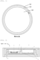
- the inventive nitride semiconductor substrate has a region A where the Ga-containing nitride semiconductor thin film 14 is not formed inward from an edge of the single crystal silicon layer 13 being a growth surface of the nitride semiconductor thin film 14.
- the substrate for film-forming can be constituted by forming the single crystal silicon layer 13 above the supporting substrate 11 via the insulative layer 12.
- a range A of the region where the film is not formed is not particularly limited, but preferably a region with 0.3 mm or longer and shorter than 3 mm inward from the edge of the single crystal silicon layer.
- a material of the insulative layer is not particularly limited, but is preferably a silicon oxide (SiO 2 ) layer.
- the nitride semiconductor thin film formed on the substrate for film-forming is not particularly limited, but preferably has: an AlN film; and a GaN film or an AlGaN film, or a both thereof formed on the AlN film.
- the substrate for film-forming preferably has: polycrystalline silicon or single crystal silicon as the supporting substrate; and the single crystal silicon layer laminated above the supporting substrate via a silicon oxide layer.
- the inventive method for manufacturing a nitride semiconductor substrate is not particularly limited as long as it comprises steps of:
- FIG. 2 illustrates a schematic view of an example of an MOCVD apparatus that can be used for the inventive method for manufacturing a semiconductor substrate.
- the MOCVD apparatus has a satellite 2 having a pocket for placing the substrate, a ceiling 3 made of quartz, and a quartz 4.
- the inventive method for manufacturing a nitride semiconductor substrate can epitaxially grow an AlN film, an AlGaN film, and a GaN film on a single crystal silicon substrate-on-insulative layer (substrate for film-forming) 1 in a rotation-revolution type MOCVD reaction furnace as illustrated in FIG. 2 , for example.
- the single crystal silicon substrate-on-insulative layer (substrate for film-forming) 1 can be placed in a wafer pocket called as the satellite 2, as illustrated in FIG. 2 for example.
- a supporting substrate and a single crystal silicon substrate for laminating are bonded via a silicon oxide layer, and then the single crystal silicon substrate for laminating is thinned to be processed into a single crystal silicon layer.
- the supporting substrate composed of a polycrystalline silicon substrate or a single crystal silicon substrate and the single crystal silicon substrate for laminating are preferably bonded via the silicon oxide layer, and then the single crystal silicon substrate for laminating is preferably processed to be thin to form the single crystal silicon layer.
- a method for thinning the single crystal silicon substrate for laminating is not particularly limited, and conventional methods can be applied. For example, after the supporting substrate and the single crystal silicon substrate for laminating are bonded via the silicon oxide layer, grinding, polishing, or etching can be performed from the surface of the single crystal silicon substrate for laminating to achieve the thinning.
- a so-called ion-implanting peeling method in which an ion-implanting layer is formed on the single crystal silicon substrate for laminating and peeled with the ion-implanting layer after the bonding.
- TMGa trimethylaluminum
- NH 3 a N source
- the carrier gas can be N 2 and H 2 , or any one thereof, and the process temperature is preferably, for example, approximately 900 to 1200°C.
- the carrier gas can be flown along a direction of a gas flow 5, and the flow rate can be regulated with a mass flow controller, etc.
- a ring-shaped member 6 is placed so as to cover the single crystal silicon layer 13 inward from an edge thereof.
- the single crystal silicon substrate-on-insulative layer substrate for film-forming 10
- the ring-shaped member 6 is placed on the silicon substrate-on-insulative layer.
- the ring-shaped member 6 is placed so as to cover the region with the single crystal silicon layer 13 of the silicon substrate-on-insulative layer (the substrate for film-forming 10), for example, 0.3 mm or longer and shorter than 3 mm from the edge.
- a lid is closed to perform the epitaxial growth.
- an AlN film is grown on the single crystal silicon layer 13, and a GaN film or an AlGaN film, or both thereof are grown on the AlN film.
- the AlN film and the AlGaN film can be formed in this order along the growing direction from the substrate side, and thereafter the GaN film can be epitaxially grown, for example.
- the structure of the epitaxial layer is not limited thereto.
- the AlGaN film is not formed, or the AlN film is further formed after forming the AlGaN film in some cases.
- FIG. 1 illustrates a positional relationship between the single crystal silicon layer 13 and the GaN layer 14 in the case where the AlN film and the GaN film are grown in this order on the single crystal silicon substrate-on-insulative layer.
- "A" in FIG. 1 represents the range not to grow the GaN film 14 by placing the ring-shaped member.
- FIG. 4 shows a relationship between a change in the width of A and a number of generated reaction marks.
- no reaction mark is generated by setting the width of A to be 0.3 mm or longer.
- the upper limit is preferably shorter than 3 mm with considering the device yield due to a reduction in the area of the GaN layer.
- a material of the ring-shaped member 6 is not particularly limited as long as it is a material durable against the reaction at a high temperature, but SiC, which causes little consumption and is almost permanently usable, is preferably used. This yields a cost merit.
- a substrate for film-forming 10 in which a single crystal silicon layer 13 is formed above a supporting substrate 11 composed of a single crystal silicon substrate with 150 mm in diameter via a silicon oxide layer 12.
- a ring-shaped member 6 composed of SiC was placed on the substrate for film-forming so as to cover a region with 0.3 mm from an edge of the single crystal silicon layer 13 of the substrate for growth.
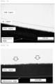
- FIG. 5 shows the result. As shown in FIG. 5 , no reaction mark was generated.
- Example 6 An epitaxial growth was performed under the same condition as in Example except that the ring-shaped member was not placed. The generation state of a reaction mark on the periphery was checked in the same manner as in Example. FIG. 6 shows the result. As shown in FIG. 6 , the generation of the reaction mark can be observed.
- the inventive nitride semiconductor substrate can be a nitride semiconductor substrate with inhibited generation of the reaction mark.
Landscapes
- Chemical & Material Sciences (AREA)
- Engineering & Computer Science (AREA)
- Crystallography & Structural Chemistry (AREA)
- Materials Engineering (AREA)
- Metallurgy (AREA)
- Organic Chemistry (AREA)
- Chemical Kinetics & Catalysis (AREA)
- General Chemical & Material Sciences (AREA)
- Inorganic Chemistry (AREA)
- Recrystallisation Techniques (AREA)
- Crystals, And After-Treatments Of Crystals (AREA)
Abstract
Description
- The present invention relates to a nitride semiconductor substrate and manufacturing method therefor.
- A MOCVD method, which is one of methods for manufacturing a semiconductor thin film is commonly used because the method has excellent large-diameter formability and mass productivity and can form a uniform thin film crystal. Nitride semiconductors represented by GaN are promising as a next-generation semiconductor material beyond the limit of a Si material. For a substrate for epitaxially growing GaN, etc. in the MOCVD method, GaN, SiC, sapphire, Si, etc. are used.
- In recent years, a substrate in which a single crystal silicon substrate is laminated onto an insulative layer (such as SiO2) (hereinafter, described as "single crystal silicon substrate-on-insulative layer"), represented by SOI, is practically applied as a substrate for epitaxially growing GaN. For example, GaN/SOI can electrically isolate each discrete part, and this insulation method is proved to eliminate a back-gate effect (which is a variation of a threshold voltage of a MOSFET due to a voltage of the substrate) and reduce switching noise. Such characteristics are merits not exhibited with the Si substrate, the GaN substrate, etc. In addition, a substrate in which a plurality of layers covers a proximity of ceramic and an insulative layer and a thin Si substrate are present on the surface side has merits of: easy control of a warp in GaN growing by a thermal expansion coefficient close to that of GaN; and hardly generated cracking or braking.
- However, the single crystal silicon substrate and the single crystal silicon substrate-on-insulative layer has a surface (GaN growth surface) made of Si, and thereby a eutectic reaction product (hereinafter, "reaction mark") between Si and Ga due to melt-back etching is likely to be generated. This reaction mark not only decreases a device yield but also probably becomes a dust source in a device process, which may contaminate a process line. Thus, it is extremely important to control generation of the reaction mark.
- Accordingly, the generation of the reaction mark is basically prevented by using a layer such as AlN on the single crystal silicon substrate, but even in this case, the reaction mark may be generated on a several positions in the wafer substrate.
Patent Document 1 discloses art for removing the reaction mark after the epitaxial growth of GaN, but does not disclose a method for controlling the reaction mark by making contrivance in the epitaxial growth. -
Patent Document 2 discloses art about forming a III-V group semiconductor thin film on the single crystal silicon substrate-on-insulative layer (SiO herein), but do not describe a reduction in defects in the film formation. There has been no literature disclosing art about a reduction in defects in forming a nitride semiconductor thin film on the single crystal silicon substrate-on-insulative layer. -
- Patent Document 1:
JP 2015-170648 A - Patent Document 2:
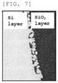
JP 2011-101007 A - When GaN is epitaxially grown on the single crystal silicon substrate-on-insulative layer as above, Si in a surface layer of the single crystal silicon substrate-on-insulative layer and Ga in trimethylgallium (TMGa) used as a Ga source may be reacted to generate the reaction mark. Compared with GaN growth on the single crystal silicon substrate alone, GaN growth on the single crystal silicon substrate-on-insulative layer tends to be likely to generate the reaction mark. This is because an edge of the surface layer of the single crystal silicon layer on the single crystal silicon substrate-on-insulative layer, which has a complex shape (
FIG. 7 ), causes a place where an AlN layer that is formed as an initial layer in forming the GaN epitaxial film is hardly formed, and bare Si is present on the edge of the single crystal silicon layer with a high possibility to be likely to allow Ga to be reacted with Si. An edge of the wafer and the edge of the single crystal silicon layer are not necessarily coincided, and the edge of the single crystal silicon layer is present inward within a certain range from the edge of the wafer in some cases. Thus, it is described as "the edge of the single crystal silicon layer". - The position where the reaction mark is generated may not only decrease the device yield but also may become a dust source in a device process to contaminate the process, and thereby the reduction is required.
- The present invention has been made to solve the above problem. An object of the present invention is to provide: a nitride semiconductor substrate with inhibited generation of the reaction mark; and a manufacturing method therefor.
- To solve the above problem, the present invention provides a nitride semiconductor substrate comprising a Ga-containing nitride semiconductor thin film formed on a substrate for film-forming in which a single crystal silicon layer is formed above a supporting substrate via an insulative layer, wherein the nitride semiconductor substrate has a region where the Ga-containing nitride semiconductor thin film is not formed inward from an edge of the single crystal silicon layer being a growth surface of the nitride semiconductor thin film.
- Such a nitride semiconductor substrate can inhibit the generation of the reaction mark due to the eutectic reaction between the single crystal silicon and Ga.
- In the present invention, the region where the film is not formed is preferably a region with 0.3 mm or longer and shorter than 3 mm inward from the edge of the single crystal silicon layer.
- Such a nitride semiconductor substrate can more improve the effect of the present invention.
- In the present invention, the insulative layer is preferably a silicon oxide (SiO2) layer.
- Such a nitride semiconductor substrate can eliminate the back-gate effect and inhibit the switching noise.
- In the present invention, the nitride semiconductor thin film formed on the substrate for film-forming preferably has: an AlN film; and a GaN film or an AlGaN film, or a both thereof formed on the AlN film.
- Such a nitride semiconductor substrate is useful as a nitride semiconductor substrate required in recent years, and can still further improve the effect of the present invention.
- In the present invention, the substrate for film-forming preferably has: polycrystalline silicon or single crystal silicon as the supporting substrate; and the single crystal silicon layer laminated above the supporting substrate via a silicon oxide layer.
- Such a nitride semiconductor substrate can further improve the effect of the present invention.
- The present invention also provides a method for manufacturing a nitride semiconductor substrate, the method comprising steps of:
- preparing at least a supporting substrate and a single crystal silicon substrate for laminating;
- bonding the supporting substrate and the single crystal silicon substrate for laminating via a silicon oxide layer;
- thinning the single crystal silicon substrate for laminating to be processed into a single crystal silicon layer;
- placing a ring-shaped member so as to cover the single crystal silicon layer inward from an edge thereof;
- growing an AlN film on the single crystal silicon layer; and
- growing a GaN film or an AlGaN film, or both thereof on the AlN film.
- Such a method for manufacturing a nitride semiconductor substrate can relatively easily manufacture the nitride semiconductor substrate with inhibited generation of the reaction mark due to the eutectic reaction between the single crystal silicon and Ga.
- In the present invention, the supporting substrate is preferably a supporting substrate composed of polycrystalline silicon or single crystal silicon.
- Such a method for manufacturing a nitride semiconductor substrate can further improve the effect of the present invention.
- As noted above, the inventive nitride semiconductor substrate can inhibit the generation of the reaction mark due to the eutectic reaction between the single crystal silicon and Ga. Therefore, a high-quality nitride semiconductor substrate can be obtained, and in manufacturing a device using this substrate, improvement of a device yield and higher precision can be attempted.
-
-
FIG. 1 is a schematic image of a top view illustrating an example of the inventive nitride semiconductor substrate. -
FIG. 2 is a schematic image illustrating an example of an MOCVD apparatus that can be used for the inventive method for manufacturing a nitride semiconductor substrate. -
FIG. 3 is a schematic sectional view illustrating an example of a substrate for film-forming of the inventive nitride semiconductor substrate. -
FIG. 4 shows a relationship between a change in a width of A illustrated inFIG. 1 and a number of generated reaction marks. -
FIG. 5 is an observation image with an optical microscope showing an edge part of a substrate formed in Example. -
FIG. 6 is an observation image with an optical microscope showing an edge part of a substrate formed in Comparative Example. -
FIG. 7 is an observation image with an optical microscope showing an edge of a surface layer of a single crystal silicon layer. - As noted above, there have been demands for development of a nitride semiconductor substrate with inhibited generation of the reaction mark and a manufacturing method therefor.
- When GaN is epitaxially grown on the single crystal silicon substrate-on-insulative layer as above, the single crystal silicon in a surface layer of the substrate for growing GaN and Ga in trimethylgallium (TMGa) used as a Ga source may be reacted to generate the reaction mark.
- The present inventors have made earnest study to solve the above problem, and have found that the generation of the reaction mark can be inhibited by providing a region where the Ga-containing nitride semiconductor thin film is not formed inward from an edge of the single crystal silicon layer being a growth surface of the nitride semiconductor thin film. This finding has led to complete the present invention.
- Specifically, the present invention is a nitride semiconductor substrate comprising a Ga-containing nitride semiconductor thin film formed on a substrate for film-forming in which a single crystal silicon layer is formed above a supporting substrate via an insulative layer, wherein the nitride semiconductor substrate has a region where the Ga-containing nitride semiconductor thin film is not formed inward from an edge of the single crystal silicon layer being a growth surface of the nitride semiconductor thin film.
- In addition, the present invention is a method for manufacturing a nitride semiconductor substrate, the method comprising steps of:
- preparing at least a supporting substrate and a single crystal silicon substrate for laminating;
- bonding the supporting substrate and the single crystal silicon substrate for laminating via a silicon oxide layer;
- thinning the single crystal silicon substrate for laminating to be processed into a single crystal silicon layer;
- placing a ring-shaped member so as to cover the single crystal silicon layer inward from an edge thereof;
- growing an AlN film on the single crystal silicon layer; and
- growing a GaN film or an AlGaN film, or both thereof on the AlN film.
- Hereinafter, the present invention will be described in detail by using the drawings, but the present invention is not limited thereto.
- A constitution of the inventive nitride semiconductor substrate is, as illustrated
FIG. 3 , a nitride semiconductor substrate in which a Ga-containing nitride semiconductor thin film is formed on a substrate for film-forming 10 in which a singlecrystal silicon layer 13 is formed above a supportingsubstrate 11 via aninsulative layer 12. As illustrated inFIG. 1 , the inventive nitride semiconductor substrate has a region A where the Ga-containing nitride semiconductorthin film 14 is not formed inward from an edge of the singlecrystal silicon layer 13 being a growth surface of the nitride semiconductorthin film 14. - As illustrated in
FIG. 3 , the substrate for film-forming can be constituted by forming the singlecrystal silicon layer 13 above the supportingsubstrate 11 via theinsulative layer 12. - A range A of the region where the film is not formed is not particularly limited, but preferably a region with 0.3 mm or longer and shorter than 3 mm inward from the edge of the single crystal silicon layer.
- A material of the insulative layer is not particularly limited, but is preferably a silicon oxide (SiO2) layer.
- The nitride semiconductor thin film formed on the substrate for film-forming is not particularly limited, but preferably has: an AlN film; and a GaN film or an AlGaN film, or a both thereof formed on the AlN film.
- In this case, the substrate for film-forming preferably has: polycrystalline silicon or single crystal silicon as the supporting substrate; and the single crystal silicon layer laminated above the supporting substrate via a silicon oxide layer.
- The inventive method for manufacturing a nitride semiconductor substrate is not particularly limited as long as it comprises steps of:
- preparing at least a supporting substrate and a single crystal silicon substrate for laminating;
- bonding the supporting substrate and the single crystal silicon substrate for laminating via a silicon oxide layer;
- thinning the single crystal silicon substrate for laminating to be processed into a single crystal silicon layer;
- placing a ring-shaped member so as to cover the single crystal silicon layer inward from an edge thereof;
- growing an AlN film on the single crystal silicon layer; and
- growing a GaN film or an AlGaN film, or both thereof on the AlN film.
-
FIG. 2 illustrates a schematic view of an example of an MOCVD apparatus that can be used for the inventive method for manufacturing a semiconductor substrate. The MOCVD apparatus has asatellite 2 having a pocket for placing the substrate, aceiling 3 made of quartz, and a quartz 4. - The inventive method for manufacturing a nitride semiconductor substrate can epitaxially grow an AlN film, an AlGaN film, and a GaN film on a single crystal silicon substrate-on-insulative layer (substrate for film-forming) 1 in a rotation-revolution type MOCVD reaction furnace as illustrated in
FIG. 2 , for example. The single crystal silicon substrate-on-insulative layer (substrate for film-forming) 1 can be placed in a wafer pocket called as thesatellite 2, as illustrated inFIG. 2 for example. - For this single crystal silicon substrate-on-
insulative layer 1, a supporting substrate and a single crystal silicon substrate for laminating are bonded via a silicon oxide layer, and then the single crystal silicon substrate for laminating is thinned to be processed into a single crystal silicon layer. For example, the supporting substrate composed of a polycrystalline silicon substrate or a single crystal silicon substrate and the single crystal silicon substrate for laminating are preferably bonded via the silicon oxide layer, and then the single crystal silicon substrate for laminating is preferably processed to be thin to form the single crystal silicon layer. - A method for thinning the single crystal silicon substrate for laminating is not particularly limited, and conventional methods can be applied. For example, after the supporting substrate and the single crystal silicon substrate for laminating are bonded via the silicon oxide layer, grinding, polishing, or etching can be performed from the surface of the single crystal silicon substrate for laminating to achieve the thinning. Alternatively, usable is a so-called ion-implanting peeling method in which an ion-implanting layer is formed on the single crystal silicon substrate for laminating and peeled with the ion-implanting layer after the bonding.
- For the epitaxial growth, trimethylaluminum (TMAl) as an Al source, TMGa as a Ga source, and NH3 as a N source can be used, for example. The carrier gas can be N2 and H2, or any one thereof, and the process temperature is preferably, for example, approximately 900 to 1200°C. The carrier gas can be flown along a direction of a gas flow 5, and the flow rate can be regulated with a mass flow controller, etc.
- In this time, a ring-shaped member 6 is placed so as to cover the single
crystal silicon layer 13 inward from an edge thereof. For example, it is acceptable that the single crystal silicon substrate-on-insulative layer (substrate for film-forming 10) is placed in the satellite, and the ring-shaped member 6 is placed on the silicon substrate-on-insulative layer. The ring-shaped member 6 is placed so as to cover the region with the singlecrystal silicon layer 13 of the silicon substrate-on-insulative layer (the substrate for film-forming 10), for example, 0.3 mm or longer and shorter than 3 mm from the edge. Thereafter, a lid is closed to perform the epitaxial growth. - In this time, an AlN film is grown on the single
crystal silicon layer 13, and a GaN film or an AlGaN film, or both thereof are grown on the AlN film. In the epitaxial layer, the AlN film and the AlGaN film can be formed in this order along the growing direction from the substrate side, and thereafter the GaN film can be epitaxially grown, for example. The structure of the epitaxial layer is not limited thereto. The AlGaN film is not formed, or the AlN film is further formed after forming the AlGaN film in some cases. -
FIG. 1 illustrates a positional relationship between the singlecrystal silicon layer 13 and theGaN layer 14 in the case where the AlN film and the GaN film are grown in this order on the single crystal silicon substrate-on-insulative layer. "A" inFIG. 1 represents the range not to grow theGaN film 14 by placing the ring-shaped member. - Here,
FIG. 4 shows a relationship between a change in the width of A and a number of generated reaction marks. As understood fromFIG. 4 , no reaction mark is generated by setting the width of A to be 0.3 mm or longer. The upper limit is preferably shorter than 3 mm with considering the device yield due to a reduction in the area of the GaN layer. - A material of the ring-shaped member 6 is not particularly limited as long as it is a material durable against the reaction at a high temperature, but SiC, which causes little consumption and is almost permanently usable, is preferably used. This yields a cost merit.
- Hereinafter, the present invention will be specifically described by using Example and Comparative Example, but the present invention is not limited thereto.
- Set in the
satellite 2 of the MOCVD apparatus illustrated inFIG. 2 was a substrate for film-forming 10 in which a singlecrystal silicon layer 13 is formed above a supportingsubstrate 11 composed of a single crystal silicon substrate with 150 mm in diameter via asilicon oxide layer 12. A ring-shaped member 6 composed of SiC was placed on the substrate for film-forming so as to cover a region with 0.3 mm from an edge of the singlecrystal silicon layer 13 of the substrate for growth. - An AlN film with 100 nm in thickness was grown thereon. Thereafter, an AlGaN layer was grown with 150 nm. A GaN layer was grown thereon, and a total thickness of the epitaxial layer was 5 um. After the epitaxial growth was finished, a proximity of the edge of the single crystal silicon layer of the substrate for film-forming with the epitaxially grown GaN film was observed with an optical microscope to check a generation state of a reaction mark.
FIG. 5 shows the result. As shown inFIG. 5 , no reaction mark was generated. - An epitaxial growth was performed under the same condition as in Example except that the ring-shaped member was not placed. The generation state of a reaction mark on the periphery was checked in the same manner as in Example.
FIG. 6 shows the result. As shown inFIG. 6 , the generation of the reaction mark can be observed. - With comparing Example and Comparative Example, the inventive nitride semiconductor substrate can be a nitride semiconductor substrate with inhibited generation of the reaction mark.
- It should be noted that the present invention is not limited to the above-described embodiments. The embodiments are just examples, and any examples that substantially have the same feature and demonstrate the same functions and effects as those in the technical concept disclosed in claims of the present invention are included in the technical scope of the present invention.
Claims (7)
- A nitride semiconductor substrate, comprising a Ga-containing nitride semiconductor thin film formed on a substrate for film-forming in which a single crystal silicon layer is formed above a supporting substrate via an insulative layer, wherein the nitride semiconductor substrate has a region where the Ga-containing nitride semiconductor thin film is not formed inward from an edge of the single crystal silicon layer being a growth surface of the nitride semiconductor thin film.
- The nitride semiconductor substrate according to claim 1, wherein the region where the film is not formed is a region with 0.3 mm or longer and shorter than 3 mm inward from the edge of the single crystal silicon layer.
- The nitride semiconductor substrate according to claim 1 or 2, wherein the insulative layer is a silicon oxide (SiO2) layer.
- The nitride semiconductor substrate according to any one of claims 1 to 3, wherein the nitride semiconductor thin film formed on the substrate for film-forming has: an AlN film; and a GaN film or an AlGaN film, or a both thereof formed on the AlN film.
- The nitride semiconductor substrate according to any one of claims 1 to 4, wherein the substrate for film-forming has: polycrystalline silicon or single crystal silicon as the supporting substrate; and the single crystal silicon layer laminated above the supporting substrate via a silicon oxide layer.
- A method for manufacturing a nitride semiconductor substrate, the method comprising steps of:preparing at least a supporting substrate and a single crystal silicon substrate for laminating;bonding the supporting substrate and the single crystal silicon substrate for laminating via a silicon oxide layer;thinning the single crystal silicon substrate for laminating to be processed into a single crystal silicon layer;placing a ring-shaped member so as to cover the single crystal silicon layer inward from an edge thereof;growing an AlN film on the single crystal silicon layer; andgrowing a GaN film or an AlGaN film, or both thereof on the AlN film.
- The method for manufacturing a nitride semiconductor substrate according to claim 6, wherein the supporting substrate is a supporting substrate composed of polycrystalline silicon or single crystal silicon.
Applications Claiming Priority (2)
| Application Number | Priority Date | Filing Date | Title |
|---|---|---|---|
| JP2021017760A JP7290156B2 (en) | 2021-02-05 | 2021-02-05 | Nitride semiconductor substrate and manufacturing method thereof |
| PCT/JP2022/001274 WO2022168573A1 (en) | 2021-02-05 | 2022-01-17 | Nitride semiconductor substrate and method for producing same |
Publications (2)
| Publication Number | Publication Date |
|---|---|
| EP4289995A1 true EP4289995A1 (en) | 2023-12-13 |
| EP4289995A4 EP4289995A4 (en) | 2025-01-15 |
Family
ID=82740617
Family Applications (1)
| Application Number | Title | Priority Date | Filing Date |
|---|---|---|---|
| EP22749450.7A Pending EP4289995A4 (en) | 2021-02-05 | 2022-01-17 | NITRIDE SEMICONDUCTOR SUBSTRATE AND PROCESS FOR PRODUCING SAME |
Country Status (7)
| Country | Link |
|---|---|
| US (1) | US20240079412A1 (en) |
| EP (1) | EP4289995A4 (en) |
| JP (1) | JP7290156B2 (en) |
| KR (1) | KR20230142717A (en) |
| CN (1) | CN116802350A (en) |
| TW (1) | TW202233914A (en) |
| WO (1) | WO2022168573A1 (en) |
Family Cites Families (27)
| Publication number | Priority date | Publication date | Assignee | Title |
|---|---|---|---|---|
| US5910339A (en) * | 1996-08-22 | 1999-06-08 | Cornell Research Foundation, Inc. | Fabrication of atomic step-free surfaces |
| US8866190B2 (en) * | 2005-06-14 | 2014-10-21 | International Rectifler Corporation | Methods of combining silicon and III-nitride material on a single wafer |
| JP2008034411A (en) * | 2006-07-26 | 2008-02-14 | Toshiba Corp | Nitride semiconductor device |
| FR2908925B1 (en) * | 2006-11-17 | 2009-02-20 | St Microelectronics Sa | METHOD FOR INTEGRATING A III-N TYPE COMPONENT, SUCH AS GAS, ON A NOMINAL SILICON (001) SUBSTRATE |
| ATE546568T1 (en) * | 2006-12-08 | 2012-03-15 | Saint Gobain Cristaux & Detecteurs | METHOD FOR PRODUCING A NITRIDE SINGLE CRYSTAL BY EPITACTICAL GROWTH ON A SUBSTRATE WHILE PREVENTING GROWTH AT THE SUBSTRATE EDGES |
| FR2917232B1 (en) * | 2007-06-06 | 2009-10-09 | Soitec Silicon On Insulator | PROCESS FOR MANUFACTURING A STRUCTURE FOR EPITAXY WITHOUT EXCLUSION AREA |
| WO2010001607A1 (en) * | 2008-07-03 | 2010-01-07 | パナソニック株式会社 | Nitride semiconductor device |
| EP2743981A1 (en) | 2009-10-30 | 2014-06-18 | Imec | Method of manufacturing an integrated semiconductor substrate structure |
| DE102009051520B4 (en) * | 2009-10-31 | 2016-11-03 | X-Fab Semiconductor Foundries Ag | Process for the production of silicon semiconductor wafers with layer structures for the integration of III-V semiconductor devices |
| JP5282978B2 (en) * | 2009-12-18 | 2013-09-04 | 日立電線株式会社 | Group III nitride semiconductor substrate |
| JP6130995B2 (en) * | 2012-02-20 | 2017-05-17 | サンケン電気株式会社 | Epitaxial substrate and semiconductor device |
| US9356045B2 (en) * | 2013-06-10 | 2016-05-31 | Raytheon Company | Semiconductor structure having column III-V isolation regions |
| JP2015050390A (en) * | 2013-09-03 | 2015-03-16 | ルネサスエレクトロニクス株式会社 | Semiconductor device |
| US9331153B2 (en) * | 2013-12-13 | 2016-05-03 | Raytheon Company | Methods and structures for forming microstrip transmission lines on thin silicon on insulator (SOI) wafers |
| JP6261388B2 (en) | 2014-03-05 | 2018-01-17 | 信越半導体株式会社 | Manufacturing method of semiconductor epitaxial wafer |
| US9735175B2 (en) * | 2015-10-09 | 2017-08-15 | International Business Machines Corporation | Integrated circuit with heterogeneous CMOS integration of strained silicon germanium and group III-V semiconductor materials and method to fabricate same |
| US20180294158A1 (en) * | 2015-12-04 | 2018-10-11 | The Silanna Group Pty Ltd | Semiconductor on insulator substrate |
| US10199216B2 (en) * | 2015-12-24 | 2019-02-05 | Infineon Technologies Austria Ag | Semiconductor wafer and method |
| KR102528559B1 (en) * | 2016-07-26 | 2023-05-04 | 삼성전자주식회사 | Apparatus for manufacturing a large size substrate |
| US11800805B2 (en) * | 2016-11-11 | 2023-10-24 | Shin-Etsu Chemical Co., Ltd. | Composite substrate, surface acoustic wave device, and method for manufacturing composite substrate |
| US10629545B2 (en) * | 2017-03-09 | 2020-04-21 | Taiwan Semiconductor Manufacturing Company Ltd. | Semiconductor device |
| US11591717B2 (en) * | 2017-09-25 | 2023-02-28 | National University Corporation Nagoya University | Vapor phase epitaxial growth device |
| US10734303B2 (en) * | 2017-11-06 | 2020-08-04 | QROMIS, Inc. | Power and RF devices implemented using an engineered substrate structure |
| GB2574879B (en) * | 2018-06-22 | 2022-12-28 | X Fab Semiconductor Foundries Gmbh | Substrates for III-nitride epitaxy |
| US20200135766A1 (en) * | 2018-10-30 | 2020-04-30 | Qualcomm Incorporated | Monolithic integration of gan hemt and si cmos |
| US11362109B2 (en) * | 2019-10-14 | 2022-06-14 | International Business Machines Corporation | Integrated power amplifier |
| US11152364B1 (en) * | 2020-04-21 | 2021-10-19 | Vanguard International Semiconductor Corporation | Semiconductor structure and methods for manufacturing the same |
-
2021
- 2021-02-05 JP JP2021017760A patent/JP7290156B2/en active Active
-
2022
- 2022-01-17 WO PCT/JP2022/001274 patent/WO2022168573A1/en not_active Ceased
- 2022-01-17 EP EP22749450.7A patent/EP4289995A4/en active Pending
- 2022-01-17 KR KR1020237026253A patent/KR20230142717A/en active Pending
- 2022-01-17 US US18/272,620 patent/US20240079412A1/en active Pending
- 2022-01-17 CN CN202280012933.5A patent/CN116802350A/en active Pending
- 2022-01-24 TW TW111102800A patent/TW202233914A/en unknown
Also Published As
| Publication number | Publication date |
|---|---|
| JP2022120695A (en) | 2022-08-18 |
| WO2022168573A1 (en) | 2022-08-11 |
| CN116802350A (en) | 2023-09-22 |
| JP7290156B2 (en) | 2023-06-13 |
| KR20230142717A (en) | 2023-10-11 |
| EP4289995A4 (en) | 2025-01-15 |
| US20240079412A1 (en) | 2024-03-07 |
| TW202233914A (en) | 2022-09-01 |
Similar Documents
| Publication | Publication Date | Title |
|---|---|---|
| JP5978548B2 (en) | Method for manufacturing gallium nitride type wafer on diamond | |
| US10796905B2 (en) | Manufacture of group IIIA-nitride layers on semiconductor on insulator structures | |
| JP5371430B2 (en) | Semiconductor substrate, method for manufacturing a self-supporting semiconductor substrate by hydride vapor phase epitaxy, and mask layer used therefor | |
| US9355852B2 (en) | Method for manufacturing semiconductor device | |
| EP3998376A1 (en) | Substrate for electronic device and production method therefor | |
| JP2005306680A (en) | Semiconductor substrate, free-standing substrate, manufacturing method thereof, and substrate polishing method | |
| US20240079412A1 (en) | Nitride semiconductor substrate and manufacturing method therefor | |
| JP2009084136A (en) | Manufacturing method of semiconductor device | |
| EP4606935A1 (en) | Method for manufacturing nitride semiconductor epitaxial wafer, and composite substrate for nitride semiconductor epitaxial wafer | |
| US8853064B2 (en) | Method of manufacturing substrate | |
| EP4289994A1 (en) | Nitride semiconductor substrate and method for producing same | |
| JP2017214232A (en) | Method of manufacturing nitride compound semiconductor substrate | |
| JP7643250B2 (en) | Nitride semiconductor substrate and method for producing same | |
| US8779437B2 (en) | Wafer, crystal growth method, and semiconductor device | |
| KR101474373B1 (en) | Semiconductor substrate and method of manufacturing the same | |
| JP6983570B2 (en) | Manufacturing method of semiconductor laminate, manufacturing method of nitride semiconductor self-supporting substrate, semiconductor laminate and semiconductor device | |
| TW202338172A (en) | Nitride semiconductor substrate and manufacturing method thereof | |
| WO2023026847A1 (en) | Nitride semiconductor substrate and method for producing same | |
| KR100839224B1 (en) | Manufacturing method of BANN thick film | |
| KR20150020498A (en) | Semiconductor substrate and method of manufacturing the same | |
| JP2014216355A (en) | Semiconductor crystal layer formation substrate and method for manufacturing composite substrate |
Legal Events
| Date | Code | Title | Description |
|---|---|---|---|
| STAA | Information on the status of an ep patent application or granted ep patent |
Free format text: STATUS: THE INTERNATIONAL PUBLICATION HAS BEEN MADE |
|
| PUAI | Public reference made under article 153(3) epc to a published international application that has entered the european phase |
Free format text: ORIGINAL CODE: 0009012 |
|
| STAA | Information on the status of an ep patent application or granted ep patent |
Free format text: STATUS: REQUEST FOR EXAMINATION WAS MADE |
|
| 17P | Request for examination filed |
Effective date: 20230717 |
|
| AK | Designated contracting states |
Kind code of ref document: A1 Designated state(s): AL AT BE BG CH CY CZ DE DK EE ES FI FR GB GR HR HU IE IS IT LI LT LU LV MC MK MT NL NO PL PT RO RS SE SI SK SM TR |
|
| DAV | Request for validation of the european patent (deleted) | ||
| DAX | Request for extension of the european patent (deleted) | ||
| A4 | Supplementary search report drawn up and despatched |
Effective date: 20241216 |
|
| RIC1 | Information provided on ipc code assigned before grant |
Ipc: H01L 21/762 20060101ALI20241210BHEP Ipc: C30B 29/06 20060101ALI20241210BHEP Ipc: C30B 29/40 20060101ALI20241210BHEP Ipc: H01L 21/20 20060101ALI20241210BHEP Ipc: C30B 25/18 20060101AFI20241210BHEP |