EP4287506A1 - Voltage ripple reduction in a power management circuit - Google Patents
Voltage ripple reduction in a power management circuit Download PDFInfo
- Publication number
- EP4287506A1 EP4287506A1 EP23174010.1A EP23174010A EP4287506A1 EP 4287506 A1 EP4287506 A1 EP 4287506A1 EP 23174010 A EP23174010 A EP 23174010A EP 4287506 A1 EP4287506 A1 EP 4287506A1
- Authority
- EP
- European Patent Office
- Prior art keywords
- voltage
- circuit
- power amplifier
- notch
- modulated
- Prior art date
- Legal status (The legal status is an assumption and is not a legal conclusion. Google has not performed a legal analysis and makes no representation as to the accuracy of the status listed.)
- Pending
Links
Images




Classifications
-
- H—ELECTRICITY
- H03—ELECTRONIC CIRCUITRY
- H03F—AMPLIFIERS
- H03F1/00—Details of amplifiers with only discharge tubes, only semiconductor devices or only unspecified devices as amplifying elements
- H03F1/02—Modifications of amplifiers to raise the efficiency, e.g. gliding Class A stages, use of an auxiliary oscillation
- H03F1/0205—Modifications of amplifiers to raise the efficiency, e.g. gliding Class A stages, use of an auxiliary oscillation in transistor amplifiers
- H03F1/0211—Modifications of amplifiers to raise the efficiency, e.g. gliding Class A stages, use of an auxiliary oscillation in transistor amplifiers with control of the supply voltage or current
- H03F1/0216—Continuous control
- H03F1/0233—Continuous control by using a signal derived from the output signal, e.g. bootstrapping the voltage supply
-
- H—ELECTRICITY
- H03—ELECTRONIC CIRCUITRY
- H03F—AMPLIFIERS
- H03F3/00—Amplifiers with only discharge tubes or only semiconductor devices as amplifying elements
- H03F3/189—High-frequency amplifiers, e.g. radio frequency amplifiers
- H03F3/19—High-frequency amplifiers, e.g. radio frequency amplifiers with semiconductor devices only
- H03F3/195—High-frequency amplifiers, e.g. radio frequency amplifiers with semiconductor devices only in integrated circuits
-
- H—ELECTRICITY
- H03—ELECTRONIC CIRCUITRY
- H03F—AMPLIFIERS
- H03F1/00—Details of amplifiers with only discharge tubes, only semiconductor devices or only unspecified devices as amplifying elements
- H03F1/02—Modifications of amplifiers to raise the efficiency, e.g. gliding Class A stages, use of an auxiliary oscillation
- H03F1/0205—Modifications of amplifiers to raise the efficiency, e.g. gliding Class A stages, use of an auxiliary oscillation in transistor amplifiers
- H03F1/0211—Modifications of amplifiers to raise the efficiency, e.g. gliding Class A stages, use of an auxiliary oscillation in transistor amplifiers with control of the supply voltage or current
- H03F1/0216—Continuous control
- H03F1/0222—Continuous control by using a signal derived from the input signal
- H03F1/0227—Continuous control by using a signal derived from the input signal using supply converters
-
- H—ELECTRICITY
- H03—ELECTRONIC CIRCUITRY
- H03F—AMPLIFIERS
- H03F3/00—Amplifiers with only discharge tubes or only semiconductor devices as amplifying elements
- H03F3/20—Power amplifiers, e.g. Class B amplifiers, Class C amplifiers
- H03F3/21—Power amplifiers, e.g. Class B amplifiers, Class C amplifiers with semiconductor devices only
-
- H—ELECTRICITY
- H03—ELECTRONIC CIRCUITRY
- H03F—AMPLIFIERS
- H03F3/00—Amplifiers with only discharge tubes or only semiconductor devices as amplifying elements
- H03F3/20—Power amplifiers, e.g. Class B amplifiers, Class C amplifiers
- H03F3/24—Power amplifiers, e.g. Class B amplifiers, Class C amplifiers of transmitter output stages
- H03F3/245—Power amplifiers, e.g. Class B amplifiers, Class C amplifiers of transmitter output stages with semiconductor devices only
-
- H—ELECTRICITY
- H03—ELECTRONIC CIRCUITRY
- H03F—AMPLIFIERS
- H03F2200/00—Indexing scheme relating to amplifiers
- H03F2200/105—A non-specified detector of the power of a signal being used in an amplifying circuit
-
- H—ELECTRICITY
- H03—ELECTRONIC CIRCUITRY
- H03F—AMPLIFIERS
- H03F2200/00—Indexing scheme relating to amplifiers
- H03F2200/451—Indexing scheme relating to amplifiers the amplifier being a radio frequency amplifier
Definitions
- the technology of the disclosure relates generally to reducing voltage ripple in a modulated voltage in a power management circuit.
- 5G-NR Fifth generation new radio
- 3G third generation
- 4G fourth generation
- a wireless communication device capable of supporting the 5G-NR wireless communication technology is expected to achieve higher data rates, improved coverage range, enhanced signaling efficiency, and reduced latency.
- Downlink and uplink transmissions in a 5G-NR system are widely based on orthogonal frequency division multiplexing (OFDM) technology.
- OFDM orthogonal frequency division multiplexing
- physical radio resources are divided into a number of subcarriers in a frequency domain and a number of OFDM symbols in a time domain.
- the subcarriers are orthogonally separated from each other by a subcarrier spacing (SCS).
- SCS subcarrier spacing
- the OFDM symbols are separated from each other by a cyclic prefix (CP), which acts as a guard band to help overcome inter-symbol interference (ISI) between the OFDM symbols.
- CP cyclic prefix
- a radio frequency (RF) signal communicated in the OFDM based system is often modulated into multiple subcarriers in the frequency domain and multiple OFDM symbols in the time domain.
- the multiple subcarriers occupied by the RF signal collectively define a modulation bandwidth of the RF signal.
- the multiple OFDM symbols define multiple time intervals during which the RF signal is communicated.
- the RF signal is typically modulated with a high modulation bandwidth in excess of 200 MHz (e.g., 1 GHz).
- the duration of an OFDM symbol depends on the SCS and the modulation bandwidth.
- Table 1 provides some OFDM symbol durations, as defined by 3G partnership project (3GPP) standards for various SCSs and modulation bandwidths. Notably, the higher the modulation bandwidth is, the shorter the OFDM symbol duration will be. For example, when the SCS is 120 KHz and the modulation bandwidth is 400 MHz, the OFDM symbol duration is 8.93 ⁇ s.
- Table 1 SCS (KHz) CP ( ⁇ s) OFDM Symbol Duration ( ⁇ s) Modulation Bandwidth (MHz) 15 4.69 71.43 50 30 2.34 35.71 100 60 1.17 17.86 200 120 0.59 8.93 400
- the wireless communication device relies on a battery cell (e.g., Li-Ion battery) to power its operations and services.
- a battery cell e.g., Li-Ion battery
- the wireless communication device can run into a low battery situation from time to time. In this regard, it is desirable to prolong battery life concurrent to enabling fast voltage changes between the OFDM symbols.
- Embodiments of the disclosure relate to voltage ripple reduction in a power management circuit.
- the power management circuit includes a power amplifier circuit configured to amplify a radio frequency (RF) signal based on a modulated voltage and an envelope tracking integrated circuit (ETIC) configured to provide the modulated voltage to the power amplifier circuit via a conductive path.
- RF radio frequency
- ETIC envelope tracking integrated circuit
- an output impedance e.g., an inductive impedance associated with the ETIC and the conductive path
- presenting at an input of the power amplifier circuit can interact with a modulated load current in the power amplifier circuit to create a voltage ripple in the modulated voltage to potentially cause an undesirable error in the RF signal.
- a notch circuit is provided, which in some implementations may appropriately be in the ETIC, to reduce the voltage ripple within a modulation bandwidth of the RF signal.
- the undesirable error such as a root-mean-square (RMS) error vector magnitude (EVM), within the modulation bandwidth of the RF signal.
- RMS root-mean-square
- EVM error vector magnitude
- a power management circuit in one aspect, includes a power amplifier circuit.
- the power amplifier circuit is configured to amplify an RF signal based on a modulated voltage received at a power amplifier input.
- the modulated voltage received at the power amplifier input comprises a voltage ripple caused by an output impedance presenting at the power amplifier input and a load current induced by the modulated voltage.
- the power management circuit also includes an ETIC.
- the ETIC is coupled to the power amplifier input via a conductive path.
- the ETIC includes a voltage modulation circuit.
- the voltage modulation circuit is configured to generate the modulated voltage at a voltage output based on a modulated target voltage.
- the ETIC also includes a notch circuit.
- the notch circuit is coupled to the power amplifier input via a notch path.
- the notch circuit is configured to resonate at a notch frequency within a modulation bandwidth of the RF signal to reduce the voltage ripple to thereby achieve a defined performance threshold.
- Embodiments of the disclosure relate to voltage ripple reduction in a power management circuit.
- the power management circuit includes a power amplifier circuit configured to amplify a radio frequency (RF) signal based on a modulated voltage and an envelope tracking integrated circuit (ETIC) configured to provide the modulated voltage to the power amplifier circuit via a conductive path.
- RF radio frequency
- ETIC envelope tracking integrated circuit
- an output impedance e.g., an inductive impedance associated with the ETIC and the conductive path
- presenting at an input of the power amplifier circuit can interact with a modulated load current in the power amplifier circuit to create a voltage ripple in the modulated voltage to potentially cause an undesirable error in the RF signal.
- a notch circuit is provided, which in some implementations may appropriately be in the ETIC, to reduce the voltage ripple within a modulation bandwidth of the RF signal.
- the undesirable error such as a root-mean-square (RMS) error vector magnitude (EVM), within the modulation bandwidth of the RF signal.
- RMS root-mean-square
- EVM error vector magnitude
- FIG. 1A is a schematic diagram of an example existing transmission circuit 10 wherein a power management circuit 12 is configured to reduce a voltage ripple V CC-RP in a modulated voltage Vcc based on a conventional approach.
- the power management circuit 12 includes an ETIC 14 and a power amplifier circuit 16.
- the ETIC 14 is configured to generate the modulated voltage Vcc based on a modulated target voltage V TGT and provide the modulated voltage Vcc to the power amplifier circuit 16 via a conductive path 18 (e.g., a conductive trace), which is coupled between a voltage output 20 of the ETIC 14 and a power amplifier input 22 of the power amplifier circuit 16.
- the power amplifier circuit 16 is configured to amplify an RF signal 24 based on the modulated voltage Vcc.
- the power amplifier input 22 may be equated with the actual voltage input 26 of the power amplifier circuit 16.
- the power management circuit 12 may be coupled to a transceiver circuit 28.
- the transceiver circuit 28 is configured to generate the RF signal 24 and the modulated target voltage V TGT .
- FIG. 1B is a schematic diagram of an example equivalent electrical model 30 of the power management circuit 12 in Figure 1A .
- Common elements between Figures 1A and 1B are shown therein with common element numbers and will not be re-described herein.
- the ETIC 14 inherently has an inductive impedance Z ETIC that can be modeled by an ETIC inductance L ETIC .
- the conductive path 18 can also be associated with an inductive trace impedance Z TRACE that can be modeled by a trace inductance L TRACE .
- the power amplifier circuit 16 looking from the power amplifier input 22 toward the ETIC 14, the power amplifier circuit 16 will see an output impedance Z OUT that includes both the inductive impedance Z ETIC and the inductive trace impedance Z TRACE .
- the power amplifier circuit 16 can be modeled as a current source.
- the power amplifier circuit 16 will modulate a load current I LOAD based on the modulated voltage Vcc.
- the load current I LOAD can interact with the output impedance Z OUT to create the voltage ripple V CC-RP in the modulated voltage Vcc received at the power amplifier input 22.
- the voltage ripple V CC-RP is a function of the modulated load current I LOAD and the output impedance Z OUT , as expressed in equation (Eq. 1) below.
- V CC ⁇ RP I LOAD * Z OUT
- Z CPA represents a capacitive impedance of the decoupling capacitor C PA .
- the capacitive impedance Z CPA and the inductive impedance Z ETIC and Z TRACE can each be determined according to equations (Eq. 3.1-3.3) below.
- Z CPA 1 / 2 ⁇ f * C PA
- Z ETIC 2 ⁇ f * L
- Z TRACE 2 ⁇ f * L TRACE
- f represents the modulation frequency of the load current I LOAD .
- the capacitive impedance Z CPA , the inductive impedance Z ETIC , and the inductive trace impedance Z TRACE are each a function of the modulation frequency f .
- Figure 1C is a graphic diagram providing an example illustration of magnitude impedance vs. the modulation frequency f .
- the output impedance Z OUT is dominated by a real part of the inductive impedance Z ETIC and a real part of the inductive trace impedance Z TRACE . Between 10 MHz and 100 MHz, the output impedance Z OUT is dominated by the inductive impedance Z ETIC and the inductive trace impedance Z TRACE . Above 1000 MHz, the output impedance Z OUT will be dominated by the capacitive impedance Z CPA .
- a modulation bandwidth BW MOD of the RF signal 24 may fall between 100 MHz and 1000 MHz (e.g., 100-500 MHz).
- the output impedance Z OUT will be determined by the output impedance Z OUT as expressed in equation (Eq. 2).
- the capacitive impedance Z CPA and therefore the output impedance Z OUT , will decrease as the capacitance C PA increases.
- the conventional approach for reducing the ripple voltage V CC-RP relies largely on adding the decoupling capacitor C PA with a larger capacitance (e.g., 1 to 2 ⁇ F). However, doing so can cause some obvious issues.
- a rate of change of the modulated voltage Vcc (denoted as ⁇ V CC or dVcc/dt) can be inversely affected by the capacitance of the decoupling capacitor C PA , as shown in equation (Eq. 4) below.
- ⁇ V CC I CC / C PA
- Ice represents a low-frequency current (a.k.a. in-rush current) provided by the ETIC 14 when the decoupling capacitor C PA is charged or discharged.
- the existing transmission circuit 10 may cause a negative impact on battery life.
- the existing transmission circuit 10 may have difficulty meeting the required rate of change ( ⁇ Vcc) of the modulated voltage Vcc, particularly when the RF signal 24 is modulated based on orthogonal frequency division multiplexing (OFDM) for transmission in a millimeter wave (mmWave) spectrum. Consequently, the existing transmission circuit 10 may not be able to change the modulated voltage Vcc in between OFDM symbols.
- ⁇ Vcc required rate of change
- FIG 2 is a schematic diagram of an example power management circuit 32 configured according to an embodiment of the present disclosure to reduce a voltage ripple V CC-RP in a modulated voltage Vcc by reducing an output impedance Z OUT presenting at a power amplifier input 34 of a power amplifier circuit 36.
- the power amplifier circuit 36 is configured to receive the modulated voltage Vcc via a conductive path 38 (e.g., a conductive trace) and amplify an RF signal 40 based on the modulated voltage Vcc.
- the power amplifier circuit 36 includes a decoupling capacitor C PA . Similar to the decoupling capacitor C PA in the power amplifier circuit 16 in Figure 1A , the decoupling capacitor C PA is also provided as close to the power amplifier input 34 as possible.
- the power management circuit 32 includes an ETIC 42.
- the ETIC 42 includes a voltage modulation circuit 44.
- the voltage modulation circuit 44 is configured to generate the modulated voltage Vcc at a voltage output 46 based on a modulated target voltage V TGT .
- the voltage output 46 is coupled to the power amplifier input 34 via the conductive path 38.
- the decoupling capacitor C PA has a capacitive impedance Z CPA
- the ETIC 42 inherently has an inductive impedance Z ETIC
- the conductive path 38 is inherently associated with an inductive trace impedance Z TRACE , which can be expressed as in the equations (Eq. 3.1-3.3).
- the power amplifier circuit 36 will see an output impedance Z OUT , as determined in the equation (Eq. 2), within a modulation bandwidth (e.g., 100-500 MHz) of the RF signal 40.
- the power amplifier circuit 36 also operates as a current source, which can induce a modulated load current I LOAD based on the modulated voltage Vcc. Similar to the power management circuit 12 in Figure 1A , the modulated load current I LOAD can interact with the output impedance Z OUT to create the voltage ripple V CC-RP in the modulated voltage Vcc received at the power amplifier input 34.
- the decoupling capacitor C PA has a smaller capacitance (e.g., 100 pF) compared to the decoupling capacitor C PA in the power amplifier circuit 16 in Figure 1A .
- the smaller decoupling capacitor C PA it is possible to improve the rate of change ( ⁇ Vcc) of the modulated voltage Vcc to satisfy the stringing voltage switching time requirement (e.g., per OFDM symbol or sub-symbol) in such advanced wireless systems as fifth generation (5G) and 5G new-radio (5G-NR), while concurrently reducing the in-rush current Ice to prolong battery life.
- the power management circuit 32 is configured to reduce the voltage ripple V CC-RP in the modulated voltage Vcc by reducing the output impedance Z OUT presenting at the power amplifier input 34 and/or creating a notch filter at the power amplifier input 34. As a result, the power management circuit 32 can achieve a defined performance threshold, such as RMS EVM and/or peak EVM within the modulation bandwidth of the RF signal 40.
- the voltage modulation circuit 44 includes a voltage amplifier 48 (denoted as "VA"), which can be an operational amplifier (OpAmp), as an example.
- VA voltage amplifier
- the voltage amplifier 48 is configured to generate an initial modulated voltage V AMP at a voltage amplifier output 50 based on the modulated target voltage V TGT and a supply voltage V SUP .
- the voltage modulation circuit 44 also includes an offset capacitor C OFF that is coupled in between the voltage amplifier output 50 and the voltage output 46.
- the voltage amplifier 48 is also configured to receive a modulated voltage feedback V CC-FB that indicates the modulated voltage Vcc at the voltage output 46, thus making the voltage modulation circuit 44 a closed-loop circuit. Accordingly, the voltage amplifier 48 can adjust the initial modulated voltage V AMP and, thus the modulated voltage Vcc, based on the modulated feedback V CC-FB to better track the modulated target voltage V TGT .
- the voltage amplifier 48 includes an input/bias stage 52 and an output stage 54.
- the output stage 54 is coupled in series to the voltage amplifier output 50.
- the output stage 54 is configured to receive a power amplifier voltage feedback V CC-PA-FB that indicates the modulated voltage Vcc as received at the power amplifier input 34.
- the output stage 54 may receive the power amplifier voltage feedback V CC-PA-FB via a feedback path 56.
- the feedback path 56 is associated with an inductive feedback trace impedance Z TRACE-FB that can be modeled by a feedback inductance L TRACE-FB .
- the power amplifier voltage feedback V CC-PA-FB since the power amplifier voltage feedback V CC-PA-FB is provided from the power amplifier input 34, the power amplifier voltage feedback V CC-PA-FB will include the voltage ripple V CC-RP in the modulated voltage Vcc as received at the power amplifier input 34. Accordingly, the voltage amplifier 48 may modify the initial modulated voltage V AMP based on the power amplifier voltage feedback V CC-PA-FB to cause the output impedance Z OUT to be reduced at the power amplifier input 34, thus helping to reduce the voltage ripple V CC-RP in the modulated voltage Vcc that is received at the power amplifier input 34.
- the ETIC 42 may include a control circuit 58, which can be a field-programmable gate array (FPGA) or an application-specific integrated circuit (ASIC), as an example.
- the control circuit 58 may control the voltage amplifier 48, for example, via a control signal 60, to modify the initial modulated voltage V AMP based on the power amplifier voltage feedback V CC-PA-FB to thereby reduce the output impedance Z OUT at the power amplifier input 34.
- Figure 3 is a schematic diagram providing an example illustration of an inner structure of the voltage amplifier 48 in Figure 2 . Common elements between Figures 2 and 3 are shown therein with common element numbers and will not be re-described herein.
- the input/bias stage 52 is configured to receive the modulated target voltage V TGT and the modulated voltage feedback V CC-FB . Accordingly, the input/bias stage 52 generates a pair of bias signals 62P, 62N to control the output stage 54.
- the output stage 54 is configured to generate the initial modulated voltage V AMP at the voltage amplifier output 50 based on a selected one of the bias signals 62P, 62N.
- the output stage 54 is also configured to receive the power amplifier voltage feedback V CC-PA-FB . Accordingly, the output stage 54 can modify the initial modulated voltage V AMP based on the power amplifier voltage feedback V CC-PA-FB to reduce the output impedance Z OUT and thereby the voltage ripple V CC-RP at the power amplifier input 34.
- the output stage 54 includes a first transistor 64P and a second transistor 64N.
- the first transistor 64P is a p-type field-effect transistor (pFET) and the second transistor 64N is an n-type FET (nFET).
- the first transistor 64P includes a first source electrode S 1 , a first drain electrode D 1 , and a first gate electrode G 1
- the second transistor 64N includes a second source electrode S 2 , a second drain electrode D 2 , and a second gate electrode G 2 .
- the first drain electrode D 1 is configured to receive the supply voltage V SUP
- the second drain electrode D2 is coupled to a ground (GND)
- the first source electrode S 1 and the second source electrode S 2 are both coupled to the voltage amplifier output 50.
- the first gate electrode G 1 is coupled to the input/bias stage 52 to receive the bias signal 62P and the second gate electrode G 2 is coupled to the input/bias stage 52 to receive the bias signal 62N.
- the input/bias stage 52 is configured to generate the bias signal 62P in response to an increase of the modulated voltage Vcc or generate the bias signal 62N in response to a decrease of the modulated voltage Vcc.
- the first transistor 64P will be turned on to output the initial modulated voltage V AMP and source a high-frequency current I AC (e.g., an alternating current) from the supply voltage V SUP in response to receiving the bias signal 62P
- the second transistor 64N will be turned on to output the initial modulated voltage V AMP from the supply voltage V SUP and sink the high-frequency current I AC to the GND in response to receiving the bias signal 62N.
- the output stage 54 also includes a first Miller capacitor C Miller1 and a second Miller capacitor C Miller2 .
- the first Miller capacitor C Miller1 is coupled between the voltage amplifier output 50 and the first gate electrode G 1
- the second Miller capacitor C Miller2 is coupled between the voltage amplifier output 50 and the second gate electrode G 2 .
- the output stage 54 can be regarded as a typical class AB rail-rail OpAmp output stage.
- the first Miller capacitor C Miller1 and the second Miller capacitor C Miller2 not only can stabilize controls of the first transistor 64P and the second transistor 64N (e.g., mitigating so-called Miller effect), but may also reduce the closed-loop output impedance of the voltage amplifier 48.
- the first Miller capacitor C Miller1 and the second Miller capacitor C Miller2 are each coupled to the voltage amplifier output 50, the first Miller capacitor C Miller1 and the second Miller capacitor C Miller2 can only reduce the inductive impedance Z ETIC , which is part of the output impedance Z OUT seen at the power amplifier input 34. As such, to further reduce the output impedance Z OUT , it is also necessary to reduce the inductive trace impedance Z TRACE .
- the output stage 54 further includes a first resistor-capacitor (RC) circuit 66P and a second RC circuit 66N.
- the first RC circuit 66P and the second RC circuit 66N are both coupled to the power amplifier input 34 via the feedback path 56 to thereby receive the power amplifier voltage feedback V CC-PA-FB .
- the first RC circuit 66P is coupled between the power amplifier input 34 and the first gate electrode G 1
- the second RC circuit 66N is coupled between the power amplifier input 34 and the second gate electrode G 2 .
- the first RC circuit 66P can cause the power amplifier voltage feedback V CC-PA-FB to be combined with the bias signal 62P to thereby modify the bias signal 62P.
- the second RC circuit 66N can cause the power amplifier voltage feedback V CC-PA-FB to be combined with the bias signal 62N to thereby modify the bias signal 62N.
- the first RC circuit 66P includes a first adjustable resistor R FB1 and a first adjustable capacitor C FB1
- the second RC circuit 66N includes a second adjustable resistor R FB2 and a second adjustable capacitor C FB2 .
- the feedback path 56 is associated with the inductive feedback trace impedance Z TRACE-FB that can be modeled by the feedback inductance L TRACE-FB .
- the first adjustable resistor R FB1 , the first adjustable capacitor C FB1 , and the feedback inductance L TRACE-FB can be equated with a first resistor-inductor-capacitor (RLC) circuit, which has a first resonance frequency f 1 as expressed in equation (Eq. 5) below.
- f 1 1 / 2 ⁇ L TRACE ⁇ FB * C FB 1
- the second adjustable resistor R FB2 , the second adjustable capacitor C FB2 , and the feedback inductance L TRACE-FB can be equated with a second RLC circuit, which has a second resonance frequency f 2 as expressed in equation (Eq. 6) below.
- f 2 1 / 2 ⁇ L TRACE ⁇ FB * C FB 2
- the first adjustable capacitor C FB1 and the second adjustable capacitor C FB2 can each be adjusted to resonate with the feedback inductance L TRACE-FB to create a low-impedance feedback path at a respective one of the first resonance frequency f 1 and the second resonance frequency f 2 .
- the first adjustable resistor R FB1 will de-Q (i.e., decrease Q-factor) the first resonance frequency f 1 across the modulation bandwidth BW MOD to prevent the first adjustable capacitor C FB1 and the feedback inductance L TRACE-FB from entering oscillation at the first resonance frequency f 1 .
- the second adjustable resistor R FB2 will de-Q (i.e., decrease Q-factor) the second resonance frequency f 2 across the modulation bandwidth BW MOD to prevent the second adjustable capacitor C FB2 and the feedback inductance L TRACE-FB from entering oscillation at the second resonance frequency f 2 .
- the first transistor 64P and the second transistor 64N may act like a common source amplifier, which amplifies and inverts the initial modulated voltage V AMP at the voltage amplifier output 50 and, therefore, the voltage output 46 of the ETIC 42.
- the inverted initial modulated voltage V AMP will cause more of the load current I LOAD to flow to the GND through the conductive path 38 (a.k.a. the trace inductor L TRACE ) than flowing through the power amplifier circuit 36, thus lowering the inductive trace impedance Z TRACE and, accordingly the output impedance Z OUT at the power amplifier input 34.
- the first adjustable capacitor C FB1 , the first adjustable resistor R FB1 , the second adjustable capacitor C FB2 , and/or the second adjustable resistor R FB2 may be adjusted by the control circuit 58 via the control signal 60.
- the power management circuit 32 can reduce an RMS value of the voltage ripple V CC-RP from 231 mV, as in the power management circuit 12 in Figure 1A , to 134 mV, which amounts to a 42% improvement.
- the ETIC 42 further includes a switcher circuit 68.
- the switcher circuit 68 includes a multi-level charge pump
- the MCP 70 which can be a buck-boost voltage converter, as an example, is configured to generate a low-frequency voltage V DC based on a battery voltage V BAT .
- the MCP 70 may operate in a buck mode to generate the low-frequency voltage V DC at 0 ⁇ V BAT or 1 ⁇ V BAT , or in a boost mode to generate the low-frequency voltage V DC at 2 ⁇ V BAT .
- the MCP 70 can generate the low-frequency voltage V DC at multiple voltage levels.
- the power inductor L P is configured to induce a low-frequency current I CC (a.k.a. in-rush current) based on the low-frequency voltage V DC .
- I CC a.k.a. in-rush current
- the low-frequency current Ice is provided to the power amplifier input 34 to charge the decoupling capacitor C PA .
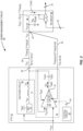
- Figure 4 is a schematic diagram of an example power management circuit 72, wherein a notch circuit 74 can be added to the power management circuit 32 of Figure 2 to further reduce the voltage ripple V CC-RP in the modulation voltage Vcc. Common elements between Figures 2 and 4 are shown therein with common element numbers and will not be re-described herein.
- the power management circuit 72 includes an ETIC 76, wherein the notch circuit 74 is provided. It should be appreciated that it is also possible for the notch circuit 74 to be integrated into the power amplifier circuit 36.
- the notch circuit 74 is coupled to the power amplifier input 34 via a notch path 78.
- the notch path 78 is also associated with an inductive notch trace impedance Z TRACE-N that can be modeled by a notch inductance L TRACE-N .
- the notch circuit 74 may be controlled by the control circuit 58, for example via a second control signal 80, to resonate at a notch frequency f NOTCH within the modulation bandwidth BW MOD to reduce the voltage ripple V CC-RP in the modulated voltage Vcc.
- the notch frequency f NOTCH may be determined by factoring in the notch inductance L TRACE-N associated with the notch path 78.
- the power management circuit 72 can achieve a defined performance threshold (e.g., RMS EVM or peak EVM).
- a simulation shows that, by adding the notch circuit 74 into the power management circuit 32 of Figure 2 , the RMS value of the voltage ripple V CC-RP can be further reduced from 134 mV to 87 mV for the 200 MHz load current modulation frequency.
- Figure 5 is a schematic diagram illustrating an example configuration of the notch circuit 74 in the power management circuit 72 of Figure 4 . Common elements between Figures 4 and 5 are shown therein with common element numbers and will not be re-described herein.
- the notch circuit 74 includes a notch capacitor C NOTCH , a notch inductor L NOTCH , and a switch circuit 82.
- the switch circuit 82 includes multiple switches S N1 -S NN , each having a respective one of multiple notch resistances R N1 -R NN .
- the notch resistances R N1 -R NN can be identical to or different from one another.
- the notch inductor L NOTCH includes multiple tap points TP 1 -TP N , each corresponding to a respective one of multiple notch inductances L N1 -L NN .
- each of the notch switches S N1 -S NN is coupled between a respective one of the tap points TP 1 -TP N and the GND.
- control circuit 58 may control the switch circuit 82 via the second control signal 80 to selectively close any of the notch switches S N1 -S NN .
- the notch resistances R N1 -R NN , the notch inductances L N1 -L NN , the notch inductance L TRACE-N , and the notch capacitance C NOTCH can be determined experimentally and/or empirically based on a target modulation of the load current I LOAD to ensure that the notch frequency f NOTCH falls within the modulation bandwidth BW MOD and the voltage ripple V CC-RP can be minimized.
- the RMS value of the voltage ripple V CC-RP can be reduced to 87 mV by setting the notch capacitance C NOTCH to 300 pF, the notch resistance R X (1 ⁇ X ⁇ N) to 1 ⁇ , and the notch inductance L X (1 ⁇ X ⁇ N) to 4 nH.
- FIG. 6 is a schematic diagram of an example user element 100 wherein the power management circuit 32 of Figure 2 and the power management circuit 72 of Figure 4 can be provided.
- the user element 100 can be any type of user elements, such as mobile terminals, smart watches, tablets, computers, navigation devices, access points, and like wireless communication devices that support wireless communications, such as cellular, wireless local area network (WLAN), Bluetooth, and near field communications.
- the user element 100 will generally include a control system 102, a baseband processor 104, transmit circuitry 106, receive circuitry 108, antenna switching circuitry 110, multiple antennas 112, and user interface circuitry 114.
- the control system 102 can be a field-programmable gate array (FPGA), as an example.
- the control system 102 can include at least a microprocessor(s), an embedded memory circuit(s), and a communication bus interface(s).
- the receive circuitry 108 receives radio frequency signals via the antennas 112 and through the antenna switching circuitry 110 from one or more base stations.
- a low noise amplifier and a filter cooperate to amplify and remove broadband interference from the received signal for processing.
- Downconversion and digitization circuitry (not shown) will then downconvert the filtered, received signal to an intermediate or baseband frequency signal, which is then digitized into one or more digital streams using analog-to-digital converter(s) (ADC).
- ADC analog-to-digital converter
- the baseband processor 104 processes the digitized received signal to extract the information or data bits conveyed in the received signal. This processing typically comprises demodulation, decoding, and error correction operations, as will be discussed in greater detail below.
- the baseband processor 104 is generally implemented in one or more digital signal processors (DSPs) and application specific integrated circuits (ASICs).
- DSPs digital signal processors
- ASICs application specific integrated circuits
- the baseband processor 104 receives digitized data, which may represent voice, data, or control information, from the control system 102, which it encodes for transmission.
- the encoded data is output to the transmit circuitry 106, where a digital-to-analog converter(s) (DAC) converts the digitally encoded data into an analog signal and a modulator modulates the analog signal onto a carrier signal that is at a desired transmit frequency or frequencies.
- DAC digital-to-analog converter
- a power amplifier will amplify the modulated carrier signal to a level appropriate for transmission, and deliver the modulated carrier signal to the antennas 112 through the antenna switching circuitry 110.
- the multiple antennas 112 and the replicated transmit and receive circuitries 106, 108 may provide spatial diversity. Modulation and processing details will be understood by those skilled in the art.
- the power management circuit includes a power amplifier circuit configured to amplify a radio frequency (RF) signal based on a modulated voltage and an envelope tracking integrated circuit (ETIC) configured to provide the modulated voltage to the power amplifier circuit via a conductive path.
- ETIC envelope tracking integrated circuit
- an output impedance presenting at an input of the power amplifier circuit can interact with a modulated load current in the power amplifier circuit to create a voltage ripple in the modulated voltage to potentially cause an undesirable error in the RF signal.
- a notch circuit is provided, which in some implementations may appropriately be in the ETIC, to reduce the voltage ripple within a modulation bandwidth of the RF signal.
- RMS root-mean-square
- EVM error vector magnitude
Landscapes
- Engineering & Computer Science (AREA)
- Power Engineering (AREA)
- Microelectronics & Electronic Packaging (AREA)
- Amplifiers (AREA)
Abstract
Description
- This application claims the benefit of
U.S. provisional patent application serial number 63/347,065, filed on May 31, 2022 U.S. patent application serial number 18/296,033, filed 5 April 2023 - The technology of the disclosure relates generally to reducing voltage ripple in a modulated voltage in a power management circuit.
- Fifth generation (5G) new radio (NR) (5G-NR) has been widely regarded as the next generation of wireless communication technology beyond the current third generation (3G) and fourth generation (4G) technologies. In this regard, a wireless communication device capable of supporting the 5G-NR wireless communication technology is expected to achieve higher data rates, improved coverage range, enhanced signaling efficiency, and reduced latency.
- Downlink and uplink transmissions in a 5G-NR system are widely based on orthogonal frequency division multiplexing (OFDM) technology. In an OFDM based system, physical radio resources are divided into a number of subcarriers in a frequency domain and a number of OFDM symbols in a time domain. The subcarriers are orthogonally separated from each other by a subcarrier spacing (SCS). The OFDM symbols are separated from each other by a cyclic prefix (CP), which acts as a guard band to help overcome inter-symbol interference (ISI) between the OFDM symbols.
- A radio frequency (RF) signal communicated in the OFDM based system is often modulated into multiple subcarriers in the frequency domain and multiple OFDM symbols in the time domain. The multiple subcarriers occupied by the RF signal collectively define a modulation bandwidth of the RF signal. The multiple OFDM symbols, on the other hand, define multiple time intervals during which the RF signal is communicated. In the 5G-NR system, the RF signal is typically modulated with a high modulation bandwidth in excess of 200 MHz (e.g., 1 GHz).
- The duration of an OFDM symbol depends on the SCS and the modulation bandwidth. The table below (Table 1) provides some OFDM symbol durations, as defined by 3G partnership project (3GPP) standards for various SCSs and modulation bandwidths. Notably, the higher the modulation bandwidth is, the shorter the OFDM symbol duration will be. For example, when the SCS is 120 KHz and the modulation bandwidth is 400 MHz, the OFDM symbol duration is 8.93 µs.
Table 1 SCS (KHz) CP (µs) OFDM Symbol Duration (µs) Modulation Bandwidth (MHz) 15 4.69 71.43 50 30 2.34 35.71 100 60 1.17 17.86 200 120 0.59 8.93 400 - Notably, the wireless communication device relies on a battery cell (e.g., Li-Ion battery) to power its operations and services. Despite recent advancement in battery technologies, the wireless communication device can run into a low battery situation from time to time. In this regard, it is desirable to prolong battery life concurrent to enabling fast voltage changes between the OFDM symbols.
- Particular aspects are set out in the appended independent claims. Various optional embodiments are set out in the dependent claims.
- Embodiments of the disclosure relate to voltage ripple reduction in a power management circuit. The power management circuit includes a power amplifier circuit configured to amplify a radio frequency (RF) signal based on a modulated voltage and an envelope tracking integrated circuit (ETIC) configured to provide the modulated voltage to the power amplifier circuit via a conductive path. Notably, an output impedance (e.g., an inductive impedance associated with the ETIC and the conductive path) presenting at an input of the power amplifier circuit can interact with a modulated load current in the power amplifier circuit to create a voltage ripple in the modulated voltage to potentially cause an undesirable error in the RF signal. In this regard, a notch circuit is provided, which in some implementations may appropriately be in the ETIC, to reduce the voltage ripple within a modulation bandwidth of the RF signal. As a result, it is possible to minimize the undesirable error, such as a root-mean-square (RMS) error vector magnitude (EVM), within the modulation bandwidth of the RF signal.
- In one aspect, a power management circuit is provided. The power management circuit includes a power amplifier circuit. The power amplifier circuit is configured to amplify an RF signal based on a modulated voltage received at a power amplifier input. The modulated voltage received at the power amplifier input comprises a voltage ripple caused by an output impedance presenting at the power amplifier input and a load current induced by the modulated voltage. The power management circuit also includes an ETIC. The ETIC is coupled to the power amplifier input via a conductive path. The ETIC includes a voltage modulation circuit. The voltage modulation circuit is configured to generate the modulated voltage at a voltage output based on a modulated target voltage. The ETIC also includes a notch circuit. The notch circuit is coupled to the power amplifier input via a notch path. The notch circuit is configured to resonate at a notch frequency within a modulation bandwidth of the RF signal to reduce the voltage ripple to thereby achieve a defined performance threshold.
- Those skilled in the art will appreciate the scope of the present disclosure and realize additional aspects thereof after reading the following detailed description of the illustrative embodiments in association with the accompanying drawing figures.
- The accompanying drawing figures incorporated in and forming a part of this specification illustrate several aspects of the disclosure, and together with the description serve to explain the principles of the disclosure.
-
Figure 1A is a schematic diagram of an example existing transmission circuit wherein a power management circuit is configured to reduce a voltage ripple in a modulated voltage based on a conventional approach; -
Figure 1B is a schematic diagram of an example electrical model of the power management circuit inFigure 1A ; -
Figure 1C is a graphic diagram providing an example illustration of magnitude impedance as a function of modulation frequency; -
Figure 2 is a schematic diagram of an example power management circuit configured according to an embodiment of the present disclosure to reduce a voltage ripple in a modulated voltage by reducing an output impedance presenting at a power amplifier input of a power amplifier circuit; -
Figure 3 is a schematic diagram providing an example illustration of an inner structure of a voltage amplifier in the power management circuit ofFigure 2 ; -
Figure 4 is a schematic diagram of an example power management circuit, wherein a notch circuit can be added to the power management circuit ofFigure 2 to further reduce the voltage ripple in the modulation voltage; -
Figure 5 is a schematic diagram illustrating an example configuration of the notch circuit inFigure 4 ; and -
Figure 6 is a schematic diagram of an example user element wherein the power management circuits ofFigures 2 and4 can be provided. - The embodiments set forth below represent the necessary information to enable those skilled in the art to practice the embodiments and illustrate the best mode of practicing the embodiments. Upon reading the following description in light of the accompanying drawing figures, those skilled in the art will understand the concepts of the disclosure and will recognize applications of these concepts not particularly addressed herein. It should be understood that these concepts and applications fall within the scope of the disclosure and the accompanying claims.
- It will be understood that, although the terms first, second, etc. may be used herein to describe various elements, these elements should not be limited by these terms. These terms are only used to distinguish one element from another. For example, a first element could be termed a second element, and, similarly, a second element could be termed a first element, without departing from the scope of the present disclosure. As used herein, the term "and/or" includes any and all combinations of one or more of the associated listed items.
- It will be understood that when an element such as a layer, region, or substrate is referred to as being "on" or extending "onto" another element, it can be directly on or extend directly onto the other element or intervening elements may also be present. In contrast, when an element is referred to as being "directly on" or extending "directly onto" another element, there are no intervening elements present. Likewise, it will be understood that when an element such as a layer, region, or substrate is referred to as being "over" or extending "over" another element, it can be directly over or extend directly over the other element or intervening elements may also be present. In contrast, when an element is referred to as being "directly over" or extending "directly over" another element, there are no intervening elements present. It will also be understood that when an element is referred to as being "connected" or "coupled" to another element, it can be directly connected or coupled to the other element or intervening elements may be present. In contrast, when an element is referred to as being "directly connected" or "directly coupled" to another element, there are no intervening elements present.
- Relative terms such as "below" or "above" or "upper" or "lower" or "horizontal" or "vertical" may be used herein to describe a relationship of one element, layer, or region to another element, layer, or region as illustrated in the Figures. It will be understood that these terms and those discussed above are intended to encompass different orientations of the device in addition to the orientation depicted in the Figures.
- The terminology used herein is for the purpose of describing particular embodiments only and is not intended to be limiting of the disclosure. As used herein, the singular forms "a," "an," and "the" are intended to include the plural forms as well, unless the context clearly indicates otherwise. It will be further understood that the terms "comprises," "comprising," "includes," and/or "including" when used herein specify the presence of stated features, integers, steps, operations, elements, and/or components, but do not preclude the presence or addition of one or more other features, integers, steps, operations, elements, components, and/or groups thereof.
- Unless otherwise defined, all terms (including technical and scientific terms) used herein have the same meaning as commonly understood by one of ordinary skill in the art to which this disclosure belongs. It will be further understood that terms used herein should be interpreted as having a meaning that is consistent with their meaning in the context of this specification and the relevant art and will not be interpreted in an idealized or overly formal sense unless expressly so defined herein.
- Embodiments of the disclosure relate to voltage ripple reduction in a power management circuit. The power management circuit includes a power amplifier circuit configured to amplify a radio frequency (RF) signal based on a modulated voltage and an envelope tracking integrated circuit (ETIC) configured to provide the modulated voltage to the power amplifier circuit via a conductive path. Notably, an output impedance (e.g., an inductive impedance associated with the ETIC and the conductive path) presenting at an input of the power amplifier circuit can interact with a modulated load current in the power amplifier circuit to create a voltage ripple in the modulated voltage to potentially cause an undesirable error in the RF signal. In this regard, a notch circuit is provided, which in some implementations may appropriately be in the ETIC, to reduce the voltage ripple within a modulation bandwidth of the RF signal. As a result, it is possible to minimize the undesirable error, such as a root-mean-square (RMS) error vector magnitude (EVM), within the modulation bandwidth of the RF signal.
- Before discussing the specific voltage ripple reduction embodiment of the present disclosure, starting at
Figure 2 , a brief overview of an existing transmission circuit is first discussed with reference toFigures 1A-1C to help understand some issues related to reducing voltage ripple based on conventional approaches. -
Figure 1A is a schematic diagram of an example existingtransmission circuit 10 wherein apower management circuit 12 is configured to reduce a voltage ripple VCC-RP in a modulated voltage Vcc based on a conventional approach. Thepower management circuit 12 includes anETIC 14 and apower amplifier circuit 16. TheETIC 14 is configured to generate the modulated voltage Vcc based on a modulated target voltage VTGT and provide the modulated voltage Vcc to thepower amplifier circuit 16 via a conductive path 18 (e.g., a conductive trace), which is coupled between avoltage output 20 of theETIC 14 and apower amplifier input 22 of thepower amplifier circuit 16. Thepower amplifier circuit 16 is configured to amplify anRF signal 24 based on the modulated voltage Vcc. - Notably, there may be an internal routing distance from the
power amplifier input 22 to an actual voltage input 26 (e.g., a collector node) of the power amplifier circuit. Given that the internal routing distance is far shorter than theconductive path 18, the internal routing distance is thus neglected hereinafter. Accordingly, thepower amplifier input 22 as illustrated herein can be equated with theactual voltage input 26 of thepower amplifier circuit 16. - The
power management circuit 12 may be coupled to atransceiver circuit 28. Herein, thetransceiver circuit 28 is configured to generate theRF signal 24 and the modulated target voltage VTGT. - The voltage ripple VCC-RP can be quantitively analyzed based on an equivalent electrical model of the
power management circuit 12. In this regard,Figure 1B is a schematic diagram of an example equivalentelectrical model 30 of thepower management circuit 12 inFigure 1A . Common elements betweenFigures 1A and1B are shown therein with common element numbers and will not be re-described herein. - The
ETIC 14 inherently has an inductive impedance ZETIC that can be modeled by an ETIC inductance LETIC. Theconductive path 18 can also be associated with an inductive trace impedance ZTRACE that can be modeled by a trace inductance LTRACE. As a result, looking from thepower amplifier input 22 toward theETIC 14, thepower amplifier circuit 16 will see an output impedance ZOUT that includes both the inductive impedance ZETIC and the inductive trace impedance ZTRACE. - The
power amplifier circuit 16 can be modeled as a current source. In this regard, thepower amplifier circuit 16 will modulate a load current ILOAD based on the modulated voltage Vcc. The load current ILOAD can interact with the output impedance ZOUT to create the voltage ripple VCC-RP in the modulated voltage Vcc received at thepower amplifier input 22. In this regard, the voltage ripple VCC-RP is a function of the modulated load current ILOAD and the output impedance ZOUT, as expressed in equation (Eq. 1) below.
- Notably from the equation (Eq. 1), it may be possible to reduce the voltage ripple VCC-RP by lowering the output impedance ZOUT seen at the
power amplifier input 22. In this regard, the conventional approach for reducing the voltage ripple VCC-RP in thepower management circuit 12 ofFigure 1A is to add a decoupling capacitor CPA inside thepower amplifier circuit 16 and be as close to thepower amplifier input 22 as possible. By adding the decoupling capacitor CPA, the output impedance ZOUT can be simply expressed as in equation (Eq. 2).
- In the equation (Eq. 2), ZCPA represents a capacitive impedance of the decoupling capacitor CPA. The capacitive impedance ZCPA and the inductive impedance ZETIC and ZTRACE can each be determined according to equations (Eq. 3.1-3.3) below.


- In the equations (Eq. 3.1-3.3), f represents the modulation frequency of the load current ILOAD. In this regard, the capacitive impedance ZCPA, the inductive impedance ZETIC, and the inductive trace impedance ZTRACE are each a function of the modulation frequency f.
Figure 1C is a graphic diagram providing an example illustration of magnitude impedance vs. the modulation frequency f. - When the modulation frequency f is lower than 10 MHz, the output impedance ZOUT is dominated by a real part of the inductive impedance ZETIC and a real part of the inductive trace impedance ZTRACE. Between 10 MHz and 100 MHz, the output impedance ZOUT is dominated by the inductive impedance ZETIC and the inductive trace impedance ZTRACE. Above 1000 MHz, the output impedance ZOUT will be dominated by the capacitive impedance ZCPA.
- Herein, a modulation bandwidth BWMOD of the
RF signal 24 may fall between 100 MHz and 1000 MHz (e.g., 100-500 MHz). In this frequency range, the output impedance ZOUT will be determined by the output impedance ZOUT as expressed in equation (Eq. 2). - Notably from equations (Eq. 2 and 3.1), the capacitive impedance ZCPA, and therefore the output impedance ZOUT, will decrease as the capacitance CPA increases. In this regard, the conventional approach for reducing the ripple voltage VCC-RP relies largely on adding the decoupling capacitor CPA with a larger capacitance (e.g., 1 to 2 µF). However, doing so can cause some obvious issues.
- Understandably, a rate of change of the modulated voltage Vcc (denoted as ΔVCC or dVcc/dt) can be inversely affected by the capacitance of the decoupling capacitor CPA, as shown in equation (Eq. 4) below.

- In the equation (Eq. 4), Ice represents a low-frequency current (a.k.a. in-rush current) provided by the
ETIC 14 when the decoupling capacitor CPA is charged or discharged. In this regard, the larger capacitance the decoupling capacitor CPA has, the larger amount of the low-frequency current Ice would be needed to change the modulated voltage Vcc at a required rate of change (ΔVcc) of the modulated voltage Vcc. As a result, the existingtransmission circuit 10 may cause a negative impact on battery life. - If the low-frequency current Ice is kept at a low level to prolong battery life, the existing
transmission circuit 10 may have difficulty meeting the required rate of change (ΔVcc) of the modulated voltage Vcc, particularly when theRF signal 24 is modulated based on orthogonal frequency division multiplexing (OFDM) for transmission in a millimeter wave (mmWave) spectrum. Consequently, the existingtransmission circuit 10 may not be able to change the modulated voltage Vcc in between OFDM symbols. - On the other hand, if the capacitance of the decoupling capacitor CPA is reduced to help improve the rate of change (ΔVcc) of the modulated voltage Vcc and reduce the in-rush current Icc, doing so may lead to insufficient reduction of the output impedance ZOUT and, thus, the voltage ripple VCC-RP. Hence, it is desirable to sufficiently reduce the ripple voltage VCC-RP within the modulation bandwidth BWMOD concurrent to improving the rate of change (ΔVcc) of the modulated voltage Vcc and reducing the in-rush current Icc.
-
Figure 2 is a schematic diagram of an examplepower management circuit 32 configured according to an embodiment of the present disclosure to reduce a voltage ripple VCC-RP in a modulated voltage Vcc by reducing an output impedance ZOUT presenting at apower amplifier input 34 of apower amplifier circuit 36. Herein, thepower amplifier circuit 36 is configured to receive the modulated voltage Vcc via a conductive path 38 (e.g., a conductive trace) and amplify anRF signal 40 based on the modulated voltage Vcc. Thepower amplifier circuit 36 includes a decoupling capacitor CPA. Similar to the decoupling capacitor CPA in thepower amplifier circuit 16 inFigure 1A , the decoupling capacitor CPA is also provided as close to thepower amplifier input 34 as possible. - The
power management circuit 32 includes anETIC 42. TheETIC 42 includes avoltage modulation circuit 44. Thevoltage modulation circuit 44 is configured to generate the modulated voltage Vcc at avoltage output 46 based on a modulated target voltage VTGT. Herein, thevoltage output 46 is coupled to thepower amplifier input 34 via theconductive path 38. - Like the
power management circuit 12 inFigure 1A , the decoupling capacitor CPA has a capacitive impedance ZCPA, theETIC 42 inherently has an inductive impedance ZETIC, and theconductive path 38 is inherently associated with an inductive trace impedance ZTRACE, which can be expressed as in the equations (Eq. 3.1-3.3). Accordingly, thepower amplifier circuit 36 will see an output impedance ZOUT, as determined in the equation (Eq. 2), within a modulation bandwidth (e.g., 100-500 MHz) of theRF signal 40. Herein, thepower amplifier circuit 36 also operates as a current source, which can induce a modulated load current ILOAD based on the modulated voltage Vcc. Similar to thepower management circuit 12 inFigure 1A , the modulated load current ILOAD can interact with the output impedance ZOUT to create the voltage ripple VCC-RP in the modulated voltage Vcc received at thepower amplifier input 34. - In embodiments disclosed herein, the decoupling capacitor CPA has a smaller capacitance (e.g., 100 pF) compared to the decoupling capacitor CPA in the
power amplifier circuit 16 inFigure 1A . By employing the smaller decoupling capacitor CPA, it is possible to improve the rate of change (ΔVcc) of the modulated voltage Vcc to satisfy the stringing voltage switching time requirement (e.g., per OFDM symbol or sub-symbol) in such advanced wireless systems as fifth generation (5G) and 5G new-radio (5G-NR), while concurrently reducing the in-rush current Ice to prolong battery life. - Further, the
power management circuit 32 is configured to reduce the voltage ripple VCC-RP in the modulated voltage Vcc by reducing the output impedance ZOUT presenting at thepower amplifier input 34 and/or creating a notch filter at thepower amplifier input 34. As a result, thepower management circuit 32 can achieve a defined performance threshold, such as RMS EVM and/or peak EVM within the modulation bandwidth of theRF signal 40. - In an embodiment, the
voltage modulation circuit 44 includes a voltage amplifier 48 (denoted as "VA"), which can be an operational amplifier (OpAmp), as an example. Thevoltage amplifier 48 is configured to generate an initial modulated voltage VAMP at avoltage amplifier output 50 based on the modulated target voltage VTGT and a supply voltage VSUP. Thevoltage modulation circuit 44 also includes an offset capacitor COFF that is coupled in between thevoltage amplifier output 50 and thevoltage output 46. The offset capacitor COFF is configured to raise the initial modulated voltage VAMP by an offset voltage VOFF to thereby generate the modulated voltage Vcc at the voltage output 46 (Vcc = VAMP + VOFF). - The
voltage amplifier 48 is also configured to receive a modulated voltage feedback VCC-FB that indicates the modulated voltage Vcc at thevoltage output 46, thus making the voltage modulation circuit 44 a closed-loop circuit. Accordingly, thevoltage amplifier 48 can adjust the initial modulated voltage VAMP and, thus the modulated voltage Vcc, based on the modulated feedback VCC-FB to better track the modulated target voltage VTGT. - The
voltage amplifier 48 includes an input/bias stage 52 and anoutput stage 54. Theoutput stage 54 is coupled in series to thevoltage amplifier output 50. According to an embodiment of the present disclosure, theoutput stage 54 is configured to receive a power amplifier voltage feedback VCC-PA-FB that indicates the modulated voltage Vcc as received at thepower amplifier input 34. In an embodiment, theoutput stage 54 may receive the power amplifier voltage feedback VCC-PA-FB via afeedback path 56. Like theconductive path 38, thefeedback path 56 is associated with an inductive feedback trace impedance ZTRACE-FB that can be modeled by a feedback inductance LTRACE-FB. - Understandably, since the power amplifier voltage feedback VCC-PA-FB is provided from the
power amplifier input 34, the power amplifier voltage feedback VCC-PA-FB will include the voltage ripple VCC-RP in the modulated voltage Vcc as received at thepower amplifier input 34. Accordingly, thevoltage amplifier 48 may modify the initial modulated voltage VAMP based on the power amplifier voltage feedback VCC-PA-FB to cause the output impedance ZOUT to be reduced at thepower amplifier input 34, thus helping to reduce the voltage ripple VCC-RP in the modulated voltage Vcc that is received at thepower amplifier input 34. - The
ETIC 42 may include acontrol circuit 58, which can be a field-programmable gate array (FPGA) or an application-specific integrated circuit (ASIC), as an example. In an embodiment, thecontrol circuit 58 may control thevoltage amplifier 48, for example, via acontrol signal 60, to modify the initial modulated voltage VAMP based on the power amplifier voltage feedback VCC-PA-FB to thereby reduce the output impedance ZOUT at thepower amplifier input 34. -
Figure 3 is a schematic diagram providing an example illustration of an inner structure of thevoltage amplifier 48 inFigure 2 . Common elements betweenFigures 2 and3 are shown therein with common element numbers and will not be re-described herein. - In an embodiment, the input/
bias stage 52 is configured to receive the modulated target voltage VTGT and the modulated voltage feedback VCC-FB. Accordingly, the input/bias stage 52 generates a pair of bias signals 62P, 62N to control theoutput stage 54. - In an embodiment, the
output stage 54 is configured to generate the initial modulated voltage VAMP at thevoltage amplifier output 50 based on a selected one of the bias signals 62P, 62N. Theoutput stage 54 is also configured to receive the power amplifier voltage feedback VCC-PA-FB. Accordingly, theoutput stage 54 can modify the initial modulated voltage VAMP based on the power amplifier voltage feedback VCC-PA-FB to reduce the output impedance ZOUT and thereby the voltage ripple VCC-RP at thepower amplifier input 34. - In an embodiment, the
output stage 54 includes afirst transistor 64P and asecond transistor 64N. In a non-limiting example, thefirst transistor 64P is a p-type field-effect transistor (pFET) and thesecond transistor 64N is an n-type FET (nFET). In this example, thefirst transistor 64P includes a first source electrode S1, a first drain electrode D1, and a first gate electrode G1, and thesecond transistor 64N includes a second source electrode S2, a second drain electrode D2, and a second gate electrode G2. Specifically, the first drain electrode D1 is configured to receive the supply voltage VSUP, the second drain electrode D2 is coupled to a ground (GND), and the first source electrode S1 and the second source electrode S2 are both coupled to thevoltage amplifier output 50. - The first gate electrode G1 is coupled to the input/
bias stage 52 to receive thebias signal 62P and the second gate electrode G2 is coupled to the input/bias stage 52 to receive thebias signal 62N. Herein, the input/bias stage 52 is configured to generate thebias signal 62P in response to an increase of the modulated voltage Vcc or generate thebias signal 62N in response to a decrease of the modulated voltage Vcc. Specifically, thefirst transistor 64P will be turned on to output the initial modulated voltage VAMP and source a high-frequency current IAC (e.g., an alternating current) from the supply voltage VSUP in response to receiving thebias signal 62P, and thesecond transistor 64N will be turned on to output the initial modulated voltage VAMP from the supply voltage VSUP and sink the high-frequency current IAC to the GND in response to receiving thebias signal 62N. - In this embodiment, the
output stage 54 also includes a first Miller capacitor CMiller1 and a second Miller capacitor CMiller2. Specifically, the first Miller capacitor CMiller1 is coupled between thevoltage amplifier output 50 and the first gate electrode G1, and the second Miller capacitor CMiller2 is coupled between thevoltage amplifier output 50 and the second gate electrode G2. In this regard, theoutput stage 54 can be regarded as a typical class AB rail-rail OpAmp output stage. The first Miller capacitor CMiller1 and the second Miller capacitor CMiller2 not only can stabilize controls of thefirst transistor 64P and thesecond transistor 64N (e.g., mitigating so-called Miller effect), but may also reduce the closed-loop output impedance of thevoltage amplifier 48. - Notably, since the first Miller capacitor CMiller1 and the second Miller capacitor CMiller2 are each coupled to the
voltage amplifier output 50, the first Miller capacitor CMiller1 and the second Miller capacitor CMiller2 can only reduce the inductive impedance ZETIC, which is part of the output impedance ZOUT seen at thepower amplifier input 34. As such, to further reduce the output impedance ZOUT, it is also necessary to reduce the inductive trace impedance ZTRACE. - In this regard, the
output stage 54 further includes a first resistor-capacitor (RC)circuit 66P and asecond RC circuit 66N. Thefirst RC circuit 66P and thesecond RC circuit 66N are both coupled to thepower amplifier input 34 via thefeedback path 56 to thereby receive the power amplifier voltage feedback VCC-PA-FB. Specifically, thefirst RC circuit 66P is coupled between thepower amplifier input 34 and the first gate electrode G1, and thesecond RC circuit 66N is coupled between thepower amplifier input 34 and the second gate electrode G2. As such, thefirst RC circuit 66P can cause the power amplifier voltage feedback VCC-PA-FB to be combined with thebias signal 62P to thereby modify thebias signal 62P. Similarly, thesecond RC circuit 66N can cause the power amplifier voltage feedback VCC-PA-FB to be combined with thebias signal 62N to thereby modify thebias signal 62N. - In an embodiment, the
first RC circuit 66P includes a first adjustable resistor RFB1 and a first adjustable capacitor CFB1, and thesecond RC circuit 66N includes a second adjustable resistor RFB2 and a second adjustable capacitor CFB2. Recall that thefeedback path 56 is associated with the inductive feedback trace impedance ZTRACE-FB that can be modeled by the feedback inductance LTRACE-FB. As such, the first adjustable resistor RFB1, the first adjustable capacitor CFB1, and the feedback inductance LTRACE-FB can be equated with a first resistor-inductor-capacitor (RLC) circuit, which has a first resonance frequency f 1 as expressed in equation (Eq. 5) below.
- Likewise, the second adjustable resistor RFB2, the second adjustable capacitor CFB2, and the feedback inductance LTRACE-FB can be equated with a second RLC circuit, which has a second resonance frequency f 2 as expressed in equation (Eq. 6) below.

- From equations (Eq. 5 and 6), the first adjustable capacitor CFB1 and the second adjustable capacitor CFB2 can each be adjusted to resonate with the feedback inductance LTRACE-FB to create a low-impedance feedback path at a respective one of the first resonance frequency f 1 and the second resonance frequency f 2. The first adjustable resistor RFB1 will de-Q (i.e., decrease Q-factor) the first resonance frequency f 1 across the modulation bandwidth BWMOD to prevent the first adjustable capacitor CFB1 and the feedback inductance LTRACE-FB from entering oscillation at the first resonance frequency f 1. Likewise, the second adjustable resistor RFB2 will de-Q (i.e., decrease Q-factor) the second resonance frequency f 2 across the modulation bandwidth BWMOD to prevent the second adjustable capacitor CFB2 and the feedback inductance LTRACE-FB from entering oscillation at the second resonance frequency f 2.
- When the voltage ripple VCC-RP seen at the
power amplifier input 34 is fed back to the first gate electrode G1 or the second gate electrode G2, thefirst transistor 64P and thesecond transistor 64N may act like a common source amplifier, which amplifies and inverts the initial modulated voltage VAMP at thevoltage amplifier output 50 and, therefore, thevoltage output 46 of theETIC 42. The inverted initial modulated voltage VAMP will cause more of the load current ILOAD to flow to the GND through the conductive path 38 (a.k.a. the trace inductor LTRACE) than flowing through thepower amplifier circuit 36, thus lowering the inductive trace impedance ZTRACE and, accordingly the output impedance ZOUT at thepower amplifier input 34. - Thus, by adjusting the first adjustable capacitor CFB1, the first adjustable resistor RFB1, the second adjustable capacitor CFB2, and/or the second adjustable resistor RFB2, it is possible to reduce the output impedance ZOUT across the modulation bandwidth BWMOD. In an embodiment, the first adjustable capacitor CFB1, the first adjustable resistor RFB1, the second adjustable capacitor CFB2, and/or the second adjustable resistor RFB2 may be adjusted by the
control circuit 58 via thecontrol signal 60. - By employing the first Miller capacitor CMiller1 and the second Miller capacitor CMiller2 to help reduce the inductive impedance ZETIC, and further employing the
first RC circuit 66P and thesecond RC circuit 66N to help reduce the inductive trace impedance ZTRACE, it is possible to reduce the output impedance ZOUT to thereby reduce the voltage ripple VCC-RP in the modulated voltage Vcc. A simulation shows that, at 200 MHz load current modulation frequency, thepower management circuit 32 can reduce an RMS value of the voltage ripple VCC-RP from 231 mV, as in thepower management circuit 12 inFigure 1A , to 134 mV, which amounts to a 42% improvement. - With reference back to
Figure 2 , theETIC 42 further includes aswitcher circuit 68. In an embodiment, theswitcher circuit 68 includes a multi-level charge pump - (MCP) 70 that is coupled to the
voltage output 46 via a power inductor LP. TheMCP 70, which can be a buck-boost voltage converter, as an example, is configured to generate a low-frequency voltage VDC based on a battery voltage VBAT. Specifically, theMCP 70 may operate in a buck mode to generate the low-frequency voltage VDC at 0×VBAT or 1×VBAT, or in a boost mode to generate the low-frequency voltage VDC at 2×VBAT. Thus, by configuring theMCP 70 to toggle between 0×VBAT, 1×VBAT, and/or 2×VBAT based on an appropriate duty cycle, theMCP 70 can generate the low-frequency voltage VDC at multiple voltage levels. - The power inductor LP is configured to induce a low-frequency current ICC (a.k.a. in-rush current) based on the low-frequency voltage VDC. As previously described in
Figure 1A , the low-frequency current Ice is provided to thepower amplifier input 34 to charge the decoupling capacitor CPA. - In addition to reducing the output impedance ZOUT to help reduce the voltage ripple VCC-RP, it is possible to further reduce the voltage ripple VCC-RP at a specific load current modulation frequency within the modulation bandwidth of the
RF signal 40 using a notch filter. In this regard,Figure 4 is a schematic diagram of an examplepower management circuit 72, wherein anotch circuit 74 can be added to thepower management circuit 32 ofFigure 2 to further reduce the voltage ripple VCC-RP in the modulation voltage Vcc. Common elements betweenFigures 2 and4 are shown therein with common element numbers and will not be re-described herein. - The
power management circuit 72 includes anETIC 76, wherein thenotch circuit 74 is provided. It should be appreciated that it is also possible for thenotch circuit 74 to be integrated into thepower amplifier circuit 36. Herein, thenotch circuit 74 is coupled to thepower amplifier input 34 via anotch path 78. Like theconductive path 38 and thefeedback path 56, thenotch path 78 is also associated with an inductive notch trace impedance ZTRACE-N that can be modeled by a notch inductance LTRACE-N. In an embodiment, thenotch circuit 74 may be controlled by thecontrol circuit 58, for example via asecond control signal 80, to resonate at a notch frequency f NOTCH within the modulation bandwidth BWMOD to reduce the voltage ripple VCC-RP in the modulated voltage Vcc. In an embodiment, the notch frequency f NOTCH may be determined by factoring in the notch inductance LTRACE-N associated with thenotch path 78. As a result, thepower management circuit 72 can achieve a defined performance threshold (e.g., RMS EVM or peak EVM). A simulation shows that, by adding thenotch circuit 74 into thepower management circuit 32 ofFigure 2 , the RMS value of the voltage ripple VCC-RP can be further reduced from 134 mV to 87 mV for the 200 MHz load current modulation frequency. -
Figure 5 is a schematic diagram illustrating an example configuration of thenotch circuit 74 in thepower management circuit 72 ofFigure 4 . Common elements betweenFigures 4 and5 are shown therein with common element numbers and will not be re-described herein. - Herein, the
notch circuit 74 includes a notch capacitor CNOTCH, a notch inductor LNOTCH, and aswitch circuit 82. Theswitch circuit 82 includes multiple switches SN1-SNN, each having a respective one of multiple notch resistances RN1-RNN. Notably, the notch resistances RN1-RNN can be identical to or different from one another. The notch inductor LNOTCH includes multiple tap points TP1-TPN, each corresponding to a respective one of multiple notch inductances LN1-LNN. Herein, each of the notch switches SN1-SNN is coupled between a respective one of the tap points TP1-TPN and the GND. Thus, by selectively closing any one of the notch switches SN1-SNN, it is possible to change the overall resistance and inductance of thenotch circuit 74 and, therefore, change the notch frequency f NOTCH of thenotch circuit 74. - In an embodiment, the
control circuit 58 may control theswitch circuit 82 via thesecond control signal 80 to selectively close any of the notch switches SN1-SNN. In a non-limiting example, the notch resistances RN1-RNN, the notch inductances LN1-LNN, the notch inductance LTRACE-N, and the notch capacitance CNOTCH can be determined experimentally and/or empirically based on a target modulation of the load current ILOAD to ensure that the notch frequency f NOTCH falls within the modulation bandwidth BWMOD and the voltage ripple VCC-RP can be minimized. For example, when the modulation bandwidth BWMOD is 200 MHz, the RMS value of the voltage ripple VCC-RP can be reduced to 87 mV by setting the notch capacitance CNOTCH to 300 pF, the notch resistance RX (1 ≦ X ≦ N) to 1 Ω, and the notch inductance LX (1 ≦ X ≦ N) to 4 nH. - The
power management circuit 32 ofFigure 2 and thepower management circuit 72 ofFigure 4 can be provided in a user element to enable bandwidth adaptation according to embodiments described above. In this regard,Figure 6 is a schematic diagram of anexample user element 100 wherein thepower management circuit 32 ofFigure 2 and thepower management circuit 72 ofFigure 4 can be provided. - Herein, the
user element 100 can be any type of user elements, such as mobile terminals, smart watches, tablets, computers, navigation devices, access points, and like wireless communication devices that support wireless communications, such as cellular, wireless local area network (WLAN), Bluetooth, and near field communications. Theuser element 100 will generally include acontrol system 102, abaseband processor 104, transmitcircuitry 106, receivecircuitry 108,antenna switching circuitry 110,multiple antennas 112, anduser interface circuitry 114. In a non-limiting example, thecontrol system 102 can be a field-programmable gate array (FPGA), as an example. In this regard, thecontrol system 102 can include at least a microprocessor(s), an embedded memory circuit(s), and a communication bus interface(s). The receivecircuitry 108 receives radio frequency signals via theantennas 112 and through theantenna switching circuitry 110 from one or more base stations. A low noise amplifier and a filter cooperate to amplify and remove broadband interference from the received signal for processing. Downconversion and digitization circuitry (not shown) will then downconvert the filtered, received signal to an intermediate or baseband frequency signal, which is then digitized into one or more digital streams using analog-to-digital converter(s) (ADC). - The
baseband processor 104 processes the digitized received signal to extract the information or data bits conveyed in the received signal. This processing typically comprises demodulation, decoding, and error correction operations, as will be discussed in greater detail below. Thebaseband processor 104 is generally implemented in one or more digital signal processors (DSPs) and application specific integrated circuits (ASICs). - For transmission, the
baseband processor 104 receives digitized data, which may represent voice, data, or control information, from thecontrol system 102, which it encodes for transmission. The encoded data is output to the transmitcircuitry 106, where a digital-to-analog converter(s) (DAC) converts the digitally encoded data into an analog signal and a modulator modulates the analog signal onto a carrier signal that is at a desired transmit frequency or frequencies. A power amplifier will amplify the modulated carrier signal to a level appropriate for transmission, and deliver the modulated carrier signal to theantennas 112 through theantenna switching circuitry 110. Themultiple antennas 112 and the replicated transmit and receivecircuitries - Therefore, from one perspective, there have been described techniques for voltage ripple reduction in a power management circuit. The power management circuit includes a power amplifier circuit configured to amplify a radio frequency (RF) signal based on a modulated voltage and an envelope tracking integrated circuit (ETIC) configured to provide the modulated voltage to the power amplifier circuit via a conductive path. Notably, an output impedance presenting at an input of the power amplifier circuit can interact with a modulated load current in the power amplifier circuit to create a voltage ripple in the modulated voltage to potentially cause an undesirable error in the RF signal. In this regard, a notch circuit is provided, which in some implementations may appropriately be in the ETIC, to reduce the voltage ripple within a modulation bandwidth of the RF signal. As a result, it is possible to minimize the undesirable error, such as root-mean-square (RMS) error vector magnitude (EVM), within the modulation bandwidth of the RF signal.
- Further examples are set out in the following numbered clauses:
-
Clause 1. A power management circuit comprising: a power amplifier circuit configured to amplify a radio frequency (RF) signal based on a modulated voltage received at a power amplifier input, wherein the modulated voltage received at the power amplifier input comprises a voltage ripple caused by an output impedance presenting at the power amplifier input and a load current induced by the modulated voltage; and an envelope tracking integrated circuit (ETIC) coupled to the power amplifier input via a conductive path and comprising: a voltage modulation circuit configured to generate the modulated voltage at a voltage output based on a modulated target voltage; and a notch circuit coupled to the power amplifier input via a notch path and configured to resonate at a notch frequency within a modulation bandwidth of the RF signal to reduce the voltage ripple to thereby achieve a defined performance threshold. - Clause 2. The power management circuit of
clause 1, wherein the ETIC further comprises a control circuit configured to determine the notch frequency and cause the notch circuit to resonate at the notch frequency. - Clause 3. The power management circuit of clause 2, wherein the control circuit is further configured to determine the notch frequency based on a target modulation of the load current within the modulation bandwidth of the RF signal to thereby minimize a root-mean-square (RMS) error vector magnitude (EVM) at the target modulation.
- Clause 4. The power management circuit of clause 2 or 3, wherein the control circuit is further configured to determine the notch frequency based on a target modulation of the load current within the modulation bandwidth of the RF signal to thereby minimize a peak error vector magnitude (EVM) at the target modulation.
- Clause 5. The power management circuit of clause 2, 3 or 4, wherein the control circuit is further configured to determine the notch frequency to factor in a notch inductance associated with the notch path.
- Clause 6. The power management circuit of any of clauses 2 to 6, wherein the notch circuit comprises: a notch capacitor coupled to the power amplifier input; a notch inductor comprising a plurality of tap points each corresponding to a respective one of a plurality of notch inductances; and a plurality of notch switches each coupled between a respective one of the plurality of tap points and a ground.
- Clause 7. The power management circuit of clause 6, wherein the control circuit is further configured to close a selected one of the plurality of notch switches to thereby cause the notch circuit to resonate at the determined notch frequency.
- Clause 8. The power management circuit of any preceding clause, wherein the voltage modulation circuit is coupled to the power amplifier input via a feedback path and further configured to: receive power amplifier voltage feedback indicating the voltage ripple in the modulated voltage received at the power amplifier input; and modify the modulated voltage based on the power amplifier voltage feedback to cause a reduction in the output impedance to thereby reduce the voltage ripple in the modulated voltage received at the power amplifier input.
- Clause 9. The power management circuit of clause 8, wherein the voltage modulation circuit comprises: a voltage amplifier configured to generate an initial modulated voltage at a voltage amplifier output based on the modulated target voltage and a supply voltage; and an offset capacitor coupled between the voltage amplifier output and the voltage output and configured to raise the initial modulated voltage by an offset voltage to thereby generate the modulated voltage at the voltage output.
-
Clause 10. The power management circuit of clause 9, wherein the voltage amplifier is further configured to: receive the power amplifier voltage feedback indicating the voltage ripple at the power amplifier input; and modify the initial modulated voltage based on the indicated voltage ripple to thereby reduce the voltage ripple in the modulated voltage. - Clause 11. The power management circuit of
clause 10, wherein the voltage amplifier comprises: an input/bias stage configured to generate a pair of bias signals based on the modulated target voltage and feedback of the modulated voltage; and an output stage configured to generate the initial modulated voltage based on a selected one of the pair of bias signals. -
Clause 12. The power management circuit of clause 11, wherein the output stage is further configured to: receive the power amplifier voltage feedback indicating the voltage ripple at the power amplifier input; and modify the initial modulated voltage based on the indicated voltage ripple to thereby reduce the voltage ripple in the modulated voltage. - Clause 13. The power management circuit of
clause 12, wherein the output stage comprises: a first transistor having a first drain electrode configured to receive the supply voltage, a first source electrode coupled to the voltage amplifier output, and a first gate electrode configured to receive a positive one of the pair of bias signals; and a second transistor having a second drain electrode coupled to a ground, a second source electrode coupled to the voltage amplifier output, and a second gate electrode configured to receive a negative one of the pair of bias signals. -
Clause 14. The power management circuit of clause 13, wherein the first transistor is a p-type field-effect transistor (pFET) and the second transistor is an n-type field-effect transistor (nFET). - Clause 15. The power management circuit of
clause 13 or 14, wherein: the first transistor is further configured to source a high-frequency current from the supply voltage in response to receiving the positive one of the pair of bias signals; and the second transistor is further configured to sink the high-frequency current from the voltage output to the ground in response to receiving the negative one of the pair of bias signals. -
Clause 16. The power management circuit ofclause 13, 14 or 15, wherein the output stage further comprises: a first Miller capacitor coupled between the voltage amplifier output and the first gate electrode; and a second Miller capacitor coupled between the voltage output and the second gate electrode. - Clause 17. The power management circuit of
clause 16, wherein the first Miller capacitor and the second Miller capacitor are configured to reduce the output impedance presenting at the power amplifier input. -
Clause 18. The power management circuit of any of clauses 13 to 17, wherein the output stage further comprises: a first resistor-capacitor circuit coupled between the power amplifier input and the first gate electrode of the first transistor; and a second resistor-capacitor circuit coupled between the power amplifier input and the second gate electrode of the second transistor. - Clause 19. The power management circuit of
clause 18, wherein: the first resistor-capacitor circuit is configured to: receive the power amplifier voltage feedback via the feedback path; and modify the positive one of the pair of bias signals based on the voltage ripple indicated in the power amplifier voltage feedback; and the second resistor-capacitor circuit is configured to: receive the power amplifier voltage feedback via the feedback path; and modify the negative one of the pair of bias signals based on the voltage ripple indicated in the power amplifier voltage feedback. -
Clause 20. The power management circuit of clause 19, wherein each of the first resistor-capacitor circuit and the second resistor-capacitor circuit comprises a respective adjustable capacitor and a respective adjustable resistor that can be adjusted to reduce the output impedance presenting at the power amplifier input. - Those skilled in the art will recognize improvements and modifications to the illustrative embodiments of the present disclosure. All such improvements and modifications are considered within the scope of the concepts disclosed herein and the claims that follow.
Claims (15)
- A power management circuit comprising:a power amplifier circuit configured to amplify a radio frequency (RF) signal based on a modulated voltage received at a power amplifier input, wherein the modulated voltage received at the power amplifier input comprises a voltage ripple caused by an output impedance presenting at the power amplifier input and a load current induced by the modulated voltage; andan envelope tracking integrated circuit (ETIC) coupled to the power amplifier input via a conductive path and comprising:a voltage modulation circuit configured to generate the modulated voltage at a voltage output based on a modulated target voltage; anda notch circuit coupled to the power amplifier input via a notch path and configured to resonate at a notch frequency within a modulation bandwidth of the RF signal to reduce the voltage ripple to thereby achieve a defined performance threshold.
- The power management circuit of claim 1, wherein the ETIC further comprises a control circuit configured to determine the notch frequency and cause the notch circuit to resonate at the notch frequency.
- The power management circuit of claim 2, wherein the control circuit is further configured to determine one or more selected from the group comprising:the notch frequency based on a target modulation of the load current within the modulation bandwidth of the RF signal to thereby minimize a root-mean-square (RMS) error vector magnitude (EVM) at the target modulation;the notch frequency based on a target modulation of the load current within the modulation bandwidth of the RF signal to thereby minimize a peak error vector magnitude (EVM) at the target modulation; andthe notch frequency to factor in a notch inductance associated with the notch path.
- The power management circuit claim 2 or 3, wherein the notch circuit comprises:a notch capacitor coupled to the power amplifier input;a notch inductor comprising a plurality of tap points each corresponding to a respective one of a plurality of notch inductances; anda plurality of notch switches each coupled between a respective one of the plurality of tap points and a ground.
- The power management circuit of claim 4, wherein the control circuit is further configured to close a selected one of the plurality of notch switches to thereby cause the notch circuit to resonate at the determined notch frequency.
- The power management circuit of any preceding claim, wherein the voltage modulation circuit is coupled to the power amplifier input via a feedback path and further configured to:receive power amplifier voltage feedback indicating the voltage ripple in the modulated voltage received at the power amplifier input; andmodify the modulated voltage based on the power amplifier voltage feedback to cause a reduction in the output impedance to thereby reduce the voltage ripple in the modulated voltage received at the power amplifier input.
- The power management circuit of claim 6, wherein the voltage modulation circuit comprises:a voltage amplifier configured to generate an initial modulated voltage at a voltage amplifier output based on the modulated target voltage and a supply voltage; andan offset capacitor coupled between the voltage amplifier output and the voltage output and configured to raise the initial modulated voltage by an offset voltage to thereby generate the modulated voltage at the voltage output.
- The power management circuit of claim 7, wherein the voltage amplifier is further configured to:receive the power amplifier voltage feedback indicating the voltage ripple at the power amplifier input; andmodify the initial modulated voltage based on the indicated voltage ripple to thereby reduce the voltage ripple in the modulated voltage.
- The power management circuit of claim 8, wherein the voltage amplifier comprises:an input/bias stage configured to generate a pair of bias signals based on the modulated target voltage and feedback of the modulated voltage; andan output stage configured to generate the initial modulated voltage based on a selected one of the pair of bias signals.
- The power management circuit of claim 9, wherein the output stage is further configured to:receive the power amplifier voltage feedback indicating the voltage ripple at the power amplifier input; andmodify the initial modulated voltage based on the indicated voltage ripple to thereby reduce the voltage ripple in the modulated voltage.
- The power management circuit of claim 10, wherein the output stage comprises:a first transistor having a first drain electrode configured to receive the supply voltage, a first source electrode coupled to the voltage amplifier output, and a first gate electrode configured to receive a positive one of the pair of bias signals; anda second transistor having a second drain electrode coupled to a ground, a second source electrode coupled to the voltage amplifier output, and a second gate electrode configured to receive a negative one of the pair of bias signals;wherein, for example, the first transistor is a p-type field-effect transistor (pFET) and the second transistor is an n-type field-effect transistor (nFET).
- The power management circuit of claim 11, wherein:the first transistor is further configured to source a high-frequency current from the supply voltage in response to receiving the positive one of the pair of bias signals; andthe second transistor is further configured to sink the high-frequency current from the voltage output to the ground in response to receiving the negative one of the pair of bias signals.
- The power management circuit of claim 11 or 12, wherein the output stage further comprises:a first Miller capacitor coupled between the voltage amplifier output and the first gate electrode; anda second Miller capacitor coupled between the voltage output and the second gate electrode;wherein, for example, the first Miller capacitor and the second Miller capacitor are configured to reduce the output impedance presenting at the power amplifier input.
- The power management circuit of claim 11, 12 or 13, wherein the output stage further comprises:a first resistor-capacitor circuit coupled between the power amplifier input and the first gate electrode of the first transistor; anda second resistor-capacitor circuit coupled between the power amplifier input and the second gate electrode of the second transistor.
- The power management circuit of claim 14, wherein:the first resistor-capacitor circuit is configured to:receive the power amplifier voltage feedback via the feedback path; andmodify the positive one of the pair of bias signals based on the voltage ripple indicated in the power amplifier voltage feedback; andthe second resistor-capacitor circuit is configured to:receive the power amplifier voltage feedback via the feedback path; andmodify the negative one of the pair of bias signals based on the voltage ripple indicated in the power amplifier voltage feedback;wherein, for example, each of the first resistor-capacitor circuit and the second resistor-capacitor circuit comprises a respective adjustable capacitor and a respective adjustable resistor that can be adjusted to reduce the output impedance presenting at the power amplifier input.
Applications Claiming Priority (2)
| Application Number | Priority Date | Filing Date | Title |
|---|---|---|---|
| US202263347065P | 2022-05-31 | 2022-05-31 | |
| US18/296,033 US12489402B2 (en) | 2022-05-31 | 2023-04-05 | Voltage ripple reduction in a power management circuit |
Publications (1)
| Publication Number | Publication Date |
|---|---|
| EP4287506A1 true EP4287506A1 (en) | 2023-12-06 |
Family
ID=86387231
Family Applications (1)
| Application Number | Title | Priority Date | Filing Date |
|---|---|---|---|
| EP23174010.1A Pending EP4287506A1 (en) | 2022-05-31 | 2023-05-17 | Voltage ripple reduction in a power management circuit |
Country Status (2)
| Country | Link |
|---|---|
| US (1) | US12489402B2 (en) |
| EP (1) | EP4287506A1 (en) |
Families Citing this family (3)
| Publication number | Priority date | Publication date | Assignee | Title |
|---|---|---|---|---|
| US12526001B2 (en) | 2022-01-18 | 2026-01-13 | Qorvo Us, Inc. | Linearized front-end operation using information from baseband circuit |
| US12381525B2 (en) * | 2022-06-28 | 2025-08-05 | Qorvo Us, Inc. | Amplifier system |
| US12456957B2 (en) | 2023-01-20 | 2025-10-28 | Qorvo Us, Inc. | Amplitude and phase error correction in a wireless communication circuit |
Citations (3)
| Publication number | Priority date | Publication date | Assignee | Title |
|---|---|---|---|---|
| US20130141062A1 (en) * | 2011-12-01 | 2013-06-06 | Rf Micro Devices, Inc. | Rf power converter |
| US20140028368A1 (en) * | 2012-07-26 | 2014-01-30 | Rf Micro Devices, Inc. | Programmable rf notch filter for envelope tracking |
| US20190245496A1 (en) * | 2018-02-06 | 2019-08-08 | Qorvo Us, Inc. | Wide modulation bandwidth radio frequency circuit |
Family Cites Families (207)
| Publication number | Priority date | Publication date | Assignee | Title |
|---|---|---|---|---|
| US4797898A (en) | 1986-11-21 | 1989-01-10 | Racal Data Communications Inc. | Method and apparatus for equalization of data transmission system |
| US6760451B1 (en) | 1993-08-03 | 2004-07-06 | Peter Graham Craven | Compensating filters |
| WO1995032561A1 (en) | 1994-05-19 | 1995-11-30 | Ortel Corporation | In-line predistorter for linearization of electronic and optical signals |
| US5793821A (en) | 1995-06-07 | 1998-08-11 | 3Com Corporation | Timing Recovery using group delay compensation |
| US6275685B1 (en) | 1998-12-10 | 2001-08-14 | Nortel Networks Limited | Linear amplifier arrangement |
| US6166601A (en) | 1999-01-07 | 2000-12-26 | Wiseband Communications Ltd. | Super-linear multi-carrier power amplifier |
| EP1104093A1 (en) | 1999-11-24 | 2001-05-30 | Telefonaktiebolaget Lm Ericsson | Method and apparatus for generation of a RF signal |
| CA2329100A1 (en) | 1999-12-21 | 2001-06-21 | Nortel Networks Limited | Phase and amplitude detector and method of determining errors |
| US6570444B2 (en) | 2000-01-26 | 2003-05-27 | Pmc-Sierra, Inc. | Low noise wideband digital predistortion amplifier |
| DE60005223T2 (en) | 2000-02-24 | 2004-07-15 | Fraunhofer-Gesellschaft zur Förderung der angewandten Forschung e.V. | DEVICE FOR PRE-DISTORMING AN INPUT SIGNAL FOR A POWER AMPLIFIER USING NON-ORTHOGONAL COORDINATES |
| US7076225B2 (en) | 2001-02-16 | 2006-07-11 | Qualcomm Incorporated | Variable gain selection in direct conversion receiver |
| US6646519B2 (en) | 2001-05-07 | 2003-11-11 | Viewsonics, Inc. | RF equalizer |
| US7049907B2 (en) | 2001-08-24 | 2006-05-23 | Powerwave Technologies, Inc. | System and method for adjusting group delay |
| US6856215B2 (en) | 2001-08-24 | 2005-02-15 | Powerwave Technologies, Inc. | System and method for adjusting group delay |
| SE0102885D0 (en) | 2001-08-28 | 2001-08-28 | Ericsson Telefon Ab L M | Calibration of an adaptive signal conditioning systern |
| US6806767B2 (en) | 2002-07-09 | 2004-10-19 | Anadigics, Inc. | Power amplifier with load switching circuit |
| ATE451795T1 (en) | 2002-07-10 | 2009-12-15 | Nxp Bv | STEREO SIGNAL PROCESSING DEVICE |
| GB2394390B (en) | 2002-10-18 | 2005-07-06 | Ipwireless Inc | Arrangement and method for RF filter |
| US7332961B2 (en) | 2002-10-22 | 2008-02-19 | Nxp B.V. | Predistortion linearizing |
| US7583754B2 (en) | 2002-10-31 | 2009-09-01 | Zte Corporation | Method and system for broadband predistortion linearization |
| CN1255938C (en) | 2002-12-10 | 2006-05-10 | 株式会社Ntt都科摩 | Linear power amplifying method and linear power amplifier |
| GB2398648B (en) | 2003-02-19 | 2005-11-09 | Nujira Ltd | Power supply stage for an amplifier |
| US7035600B2 (en) | 2003-06-19 | 2006-04-25 | Harris Corporation | Digitally adaptive modulated transmitter |
| US7522658B2 (en) | 2003-09-30 | 2009-04-21 | Broadcom Corporation | Design method and implementation of optimal linear IIR equalizers for RF transceivers |
| US7397863B2 (en) | 2003-09-30 | 2008-07-08 | Broadcom Corporation | Implementation technique for linear phase equalization in multi-mode RF transmitters |
| US7430248B2 (en) | 2004-01-27 | 2008-09-30 | Crestcom, Inc. | Predistortion circuit and method for compensating nonlinear distortion in a digital RF communications transmitter |
| SE0402289D0 (en) | 2004-09-21 | 2004-09-21 | Ericsson Telefon Ab L M | predistorter |
| US7336723B2 (en) | 2004-11-08 | 2008-02-26 | Photron Research And Development Pte Ltd. | Systems and methods for high-efficiency transmission of information through narrowband channels |
| WO2006087864A1 (en) | 2005-02-17 | 2006-08-24 | Hitachi Kokusai Electric Inc. | Predistorter |
| US7193462B2 (en) | 2005-03-22 | 2007-03-20 | Powerwave Technologies, Inc. | RF power amplifier system employing an analog predistortion module using zero crossings |
| JP5301831B2 (en) | 2005-06-30 | 2013-09-25 | 富士通株式会社 | Power amplifier having distortion compensation circuit |
| KR101002893B1 (en) | 2005-08-06 | 2010-12-21 | 삼성전자주식회사 | Multimode Power Amplification Method and Apparatus Using Predistorter |
| CN101258690A (en) | 2005-09-06 | 2008-09-03 | 三菱电机株式会社 | Leakage Signal Cancellation Device |
| US7831221B2 (en) | 2005-12-13 | 2010-11-09 | Andrew Llc | Predistortion system and amplifier for addressing group delay modulation |
| US7889820B2 (en) | 2006-01-05 | 2011-02-15 | Qualcomm Incorporated | Phase compensation for analog gain switching in OFDM modulated physical channel |
| US7933570B2 (en) | 2006-02-03 | 2011-04-26 | Quantance, Inc. | Power amplifier controller circuit |
| CA2576778C (en) | 2006-02-07 | 2014-09-02 | Xinping Huang | Self-calibrating multi-port circuit and method |
| CN100492921C (en) | 2006-05-30 | 2009-05-27 | 华为技术有限公司 | Receiver and method for receiving radio signal |
| US7471204B2 (en) | 2006-07-07 | 2008-12-30 | Broadcom Corporation | Receiver architecture for canceling blocking signals |
| US7945208B2 (en) | 2006-08-14 | 2011-05-17 | Gct Semiconductor, Inc. | Radio frequency integrated circuit |
| US7830220B2 (en) | 2006-09-26 | 2010-11-09 | Infineon Technologies Ag | Modulator arrangement and method for signal modulation |
| KR20100014339A (en) | 2006-12-26 | 2010-02-10 | 달리 시스템즈 씨오. 엘티디. | Method and system for baseband predistortion linearization in multi-channel wideband communication systems |
| US8400338B2 (en) | 2006-12-29 | 2013-03-19 | Teradyne, Inc. | Compensating for harmonic distortion in an instrument channel |
| US20120244824A1 (en) | 2007-02-12 | 2012-09-27 | Texas Instruments Incorporated | Minimization of rms phase error in a phase locked loop by dithering of a frequency reference |
| US7755429B2 (en) | 2007-02-16 | 2010-07-13 | Microelectronics Technology Inc. | System and method for dynamic drain voltage adjustment to control linearity, output power, and efficiency in RF power amplifiers |
| US7688157B2 (en) | 2007-04-05 | 2010-03-30 | Panasonic Corporation | Selective envelope modulation enabling reduced current consumption |
| US20090004981A1 (en) | 2007-06-27 | 2009-01-01 | Texas Instruments Incorporated | High efficiency digital transmitter incorporating switching power supply and linear power amplifier |
| US7859338B2 (en) | 2007-07-26 | 2010-12-28 | Broadcom Corporation | Compact low-power class AB amplifier |
| US20090061787A1 (en) | 2007-08-30 | 2009-03-05 | Rainer Koller | Transceiver, rf-transceiver, communication system and method for transferring control packets |
| US8059748B2 (en) | 2007-09-19 | 2011-11-15 | Qualcomm, Incorporated | Multi-mode and multi-band transmitters for wireless communication |
| US7739063B2 (en) | 2007-11-14 | 2010-06-15 | Agilent Technologies, Inc. | Nonlinear measurement system error correction |
| FI20075958A0 (en) | 2007-12-21 | 2007-12-21 | Nokia Corp | Processing of broadcast signals in a radio transmitter |
| US9705477B2 (en) | 2008-04-30 | 2017-07-11 | Innovation Digital, LLC | Compensator for removing nonlinear distortion |
| CA2668264A1 (en) | 2008-06-05 | 2009-12-05 | Raytheon Canada Limited | Linearizing technique for power amplifiers |
| US8374282B2 (en) | 2008-07-24 | 2013-02-12 | Motorola Mobility Llc | Method and apparatus for improving digital predistortion correction with amplifier device biasing |
| US8184751B2 (en) | 2008-12-03 | 2012-05-22 | Bae Systems Information And Electronic Systems Integration Inc. | Integrated interference cancellation system architecture with distortion correction |
| EP2252003A1 (en) | 2009-05-12 | 2010-11-17 | CoreOptics Inc. | Phase detection method and phase detector |
| US8385854B2 (en) | 2009-05-21 | 2013-02-26 | Qualcomm Incorporated | Adaptive parametric power amplifier protection circuit |
| US7978009B2 (en) | 2009-08-03 | 2011-07-12 | Telefonaktiebolaget Lm Ericsson (Publ) | Digital modulated RF power amplifier with impedance compensation circuit |
| CN101651459B (en) | 2009-09-15 | 2013-02-13 | 电子科技大学 | High-efficiency linear LINC transmitter |
| KR101087629B1 (en) | 2009-12-30 | 2011-11-30 | 광주과학기술원 | Multi-Band Power Amplifiers |
| JPWO2011086752A1 (en) | 2010-01-14 | 2013-05-16 | 住友電気工業株式会社 | Amplifying device and signal processing device |
| JP5487996B2 (en) | 2010-01-25 | 2014-05-14 | 富士通株式会社 | Adaptive equalizer and adaptive equalization method |
| JP2011188123A (en) | 2010-03-05 | 2011-09-22 | Panasonic Corp | Transmitter circuit using polar modulation method, and communication device |
| KR101093864B1 (en) | 2010-03-18 | 2011-12-13 | 한국방송공사 | Automatic linear and nonlinear distortion compensation device and method |
| JP2011211533A (en) | 2010-03-30 | 2011-10-20 | Sumitomo Electric Ind Ltd | Amplifier circuit and radio communication apparatus |
| WO2011133542A1 (en) | 2010-04-19 | 2011-10-27 | Rf Micro Devices, Inc. | Pseudo-envelope following power management system |
| US8831544B2 (en) | 2010-04-20 | 2014-09-09 | Rf Micro Devices, Inc. | Dynamic device switching (DDS) of an in-phase RF PA stage and a quadrature-phase RF PA stage |
| JP5402817B2 (en) | 2010-04-30 | 2014-01-29 | 富士通株式会社 | Power amplifier memory effect canceller, wireless transmitter |
| GB2480687B (en) | 2010-05-28 | 2018-04-04 | Snaptrack Inc | Power supply pre-distortion |
| US8749309B2 (en) | 2010-12-05 | 2014-06-10 | Rf Micro Devices (Cayman Islands), Ltd. | Gate-based output power level control power amplifier |
| US8975960B2 (en) | 2011-02-01 | 2015-03-10 | Mediatek Singapore Pte. Ltd. | Integrated circuit wireless communication unit and method for providing a power supply |
| US9379667B2 (en) | 2011-05-05 | 2016-06-28 | Rf Micro Devices, Inc. | Multiple power supply input parallel amplifier based envelope tracking |
| WO2012151594A2 (en) | 2011-05-05 | 2012-11-08 | Rf Micro Devices, Inc. | Power managent system for pseudo-envelope and average power tracking |
| US10263628B2 (en) | 2011-06-27 | 2019-04-16 | Syntropy Systems, Llc | Apparatuses and methods for converting fluctuations in periodicity of an input signal into fluctuations in amplitude of an output signal |
| US10623014B2 (en) | 2011-06-27 | 2020-04-14 | Syntropy Systems, Llc | Apparatuses and methods for sample rate conversion |
| KR101784885B1 (en) | 2011-10-14 | 2017-10-13 | 삼성전자주식회사 | Apparatus and method apparatus for interleaving switching in power amplifier |
| US9065504B2 (en) | 2011-10-28 | 2015-06-23 | Broadcom Corporation | Transmitter front end with programmable notch filter and methods for use therewith |
| US8649745B2 (en) | 2011-12-21 | 2014-02-11 | Telefonaktiebolaget L M Ericsson (Publ) | Adaptive predistortion for a non-linear subsystem based on a model as a concatenation of a non-linear model followed by a linear model |
| US9001947B2 (en) | 2012-01-10 | 2015-04-07 | Telefonaktiebolaget L M Ericsson (Publ) | Linearization of multi-antenna receivers with RF pre-distortion |
| US8952753B2 (en) | 2012-02-17 | 2015-02-10 | Quantance, Inc. | Dynamic power supply employing a linear driver and a switching regulator |
| JP5591853B2 (en) | 2012-03-19 | 2014-09-17 | 株式会社東芝 | Quadrature error compensation circuit |
| CN107612663B (en) | 2012-05-10 | 2021-01-29 | 瑞典爱立信有限公司 | Method and apparatus for hybrid automatic repeat request signaling for carrier aggregation |
| US9225296B2 (en) | 2012-07-23 | 2015-12-29 | Dali Systems Co. Ltd. | Method and system for aligning signals widely spaced in frequency for wideband digital predistortion in wireless communication systems |
| US20140029683A1 (en) | 2012-07-26 | 2014-01-30 | Telefonaktiebolaget L M Ericsson (Publ) | Multi-Band Observation Receiver |
| US9276475B2 (en) | 2012-08-10 | 2016-03-01 | Texas Instruments Incorporated | Switched mode assisted linear regulator with decoupled output impedance and signal path bandwidth |
| JP6315834B2 (en) | 2012-08-10 | 2018-04-25 | 日本テキサス・インスツルメンツ株式会社 | Switched mode assist linear regulator |
| JP2014045371A (en) | 2012-08-27 | 2014-03-13 | Fujitsu Ltd | Power amplification device |
| US8824980B2 (en) | 2012-09-05 | 2014-09-02 | Analog Devices, Inc. | System and method to implement a radio transmitter with digital predistortion having reduced noise |
| US8952795B2 (en) | 2012-09-06 | 2015-02-10 | OmniVision Technologies | Selective gain control circuit |
| US9300407B2 (en) | 2012-09-07 | 2016-03-29 | Futurewei Technologies, Inc. | Channel estimation for optical orthogonal frequency division multiplexing systems |
| US8760222B2 (en) | 2012-09-24 | 2014-06-24 | Motorola Mobility Llc | Method and apparatus for controlling or managing bandwidth of a filter circuit within a system having two integrated circuits |
| US8934856B2 (en) | 2012-10-12 | 2015-01-13 | Analog Devices, Inc. | System and method to calibrate the frequency response of an electronic filter |
| US9560595B2 (en) | 2012-12-03 | 2017-01-31 | Broadcom Corporation | Dynamic operating bandwidth configuration for an envelope tracker |
| US9287829B2 (en) | 2012-12-28 | 2016-03-15 | Peregrine Semiconductor Corporation | Control systems and methods for power amplifiers operating in envelope tracking mode |
| US8824981B2 (en) | 2013-01-31 | 2014-09-02 | Intel Mobile Communications GmbH | Recalibration of envelope tracking transfer function during active transmission |
| US9391565B2 (en) | 2013-03-15 | 2016-07-12 | TriQuint International PTE, Ltd. | Amplifier phase distortion correction based on amplitude distortion measurement |
| JP6107358B2 (en) | 2013-04-17 | 2017-04-05 | 富士通株式会社 | Power supply circuit, power supply IC, power amplification device, and wireless communication device |
| US9461596B1 (en) | 2013-05-31 | 2016-10-04 | Skyworks Solutions, Inc. | Doherty power amplifier with integrated pre-distortion |
| US9036734B1 (en) | 2013-07-22 | 2015-05-19 | Altera Corporation | Methods and apparatus for performing digital predistortion using time domain and frequency domain alignment |
| US9197168B2 (en) | 2013-07-23 | 2015-11-24 | Mstar Semiconductor, Inc. | Amplitude modulation to phase modulation (AMPM) distortion compensation |
| US9124315B2 (en) | 2013-11-05 | 2015-09-01 | At&T Mobility Ii Llc | Compressed amplitude wireless signal and compression function |
| JP2015099972A (en) | 2013-11-18 | 2015-05-28 | 三菱電機株式会社 | Transmitter module |
| US9438196B2 (en) | 2014-02-14 | 2016-09-06 | Peregrine Semiconductor Corporation | Integrated tunable filter architecture |
| US10333474B2 (en) | 2014-05-19 | 2019-06-25 | Skyworks Solutions, Inc. | RF transceiver front end module with improved linearity |
| US9692366B2 (en) | 2014-12-09 | 2017-06-27 | Intel Corporation | Envelope tracking path delay fine tuning and calibration |
| US9425742B2 (en) | 2014-12-10 | 2016-08-23 | Intel Corporation | Method and apparatus for correcting inconvenient power amplifier load characteristics in an envelope tracking based system |
| US9930725B2 (en) | 2014-12-16 | 2018-03-27 | Apple Inc. | Wireless electronic device with multiradio controller integrated circuit |
| US20160182099A1 (en) | 2014-12-23 | 2016-06-23 | Honeywell International Inc. | Systems and methods for efficient multi-channel satcom with dynamic power supply and digital pre-distortion |
| DE102014119625A1 (en) | 2014-12-23 | 2016-06-23 | Intel IP Corporation | Circuit and method for providing a radio frequency signal |
| CN105812073A (en) | 2014-12-31 | 2016-07-27 | 上海贝尔股份有限公司 | Horizontal and vertical combined calibration method and device for active antenna array |
| JP6565288B2 (en) | 2015-04-10 | 2019-08-28 | 富士通株式会社 | Wireless device |
| JP2016213603A (en) | 2015-05-01 | 2016-12-15 | 富士通株式会社 | Wireless communication device |
| US9800274B2 (en) | 2015-07-03 | 2017-10-24 | Mediatek, Inc. | Communication units and methods for power supply control |
| US9660675B2 (en) | 2015-10-13 | 2017-05-23 | Analog Devices Global | Digital predistortion and uptilt and cable communication |
| US9673847B1 (en) | 2015-11-25 | 2017-06-06 | Analog Devices, Inc. | Apparatus and methods for transceiver calibration |
| US10716080B2 (en) | 2016-02-09 | 2020-07-14 | Apple Inc. | Calibration techniques for envelope tracking power amplifiers |
| EP3427417B1 (en) | 2016-03-07 | 2022-05-11 | Satixfy UK Limited | Calibration techniques for an antenna array |
| US10033413B2 (en) | 2016-05-19 | 2018-07-24 | Analog Devices Global | Mixed-mode digital predistortion |
| EP3252949B1 (en) | 2016-06-01 | 2020-03-18 | Intel IP Corporation | Methods and devices for predistortion of signals |
| JP6446501B2 (en) | 2016-06-07 | 2018-12-26 | メレクシス・テクノロジーズ・ソシエテ・アノニムMelexis Technologies Sa | Drive circuit for passive resonant circuit and transmitter device |
| US10097138B2 (en) | 2016-07-26 | 2018-10-09 | Nxp Usa, Inc. | Doherty input power splitter and linearization method |
| GB2598210B (en) | 2016-08-31 | 2022-09-21 | Skyworks Solutions Inc | Multi-input amplifier with degeneration switching block and low loss bypass function |
| US10333479B2 (en) | 2016-12-16 | 2019-06-25 | Qorvo Us, Inc. | Power amplifier with improved linearity |
| US10181478B2 (en) | 2017-01-06 | 2019-01-15 | Qorvo Us, Inc. | Radio frequency switch having field effect transistor cells |
| JP6680235B2 (en) | 2017-02-09 | 2020-04-15 | 株式会社村田製作所 | Power amplifier circuit and high frequency module |
| US11223376B2 (en) | 2017-02-27 | 2022-01-11 | Apple Inc. | Frequency dependent envelope tracking |
| US9973370B1 (en) | 2017-06-06 | 2018-05-15 | Intel IP Corporation | Memory predistortion in bandwidth limited envelope tracking |
| JP6448881B1 (en) | 2017-06-29 | 2019-01-09 | 三菱電機株式会社 | Distortion compensation device |
| TWI639299B (en) | 2017-08-02 | 2018-10-21 | 立積電子股份有限公司 | Current compensation circuit |
| CN107483021B (en) | 2017-08-15 | 2020-09-08 | 广州联星科技有限公司 | Linear correction circuit, correction method and device for analog predistortion power amplifier |
| US10326490B2 (en) | 2017-08-31 | 2019-06-18 | Qorvo Us, Inc. | Multi radio access technology power management circuit |
| US10778345B2 (en) | 2017-09-11 | 2020-09-15 | Apple, Inc. | Dynamic look up table measurements for transmitter with envelope tracking systems |
| US10326408B2 (en) | 2017-09-18 | 2019-06-18 | Qorvo Us, Inc. | Envelope tracking power management circuit |
| US20190097671A1 (en) | 2017-09-26 | 2019-03-28 | Apple Inc. | Converged transmitter architecture with reduced power consumption |
| US10432145B2 (en) | 2018-01-15 | 2019-10-01 | Qorvo Us, Inc. | Envelope tracking circuit |
| US11424718B2 (en) | 2018-03-01 | 2022-08-23 | Telefonaktiebolaget Lm Ericsson (Publ) | Envelope tracking supply modulator for power amplifier |
| US10361744B1 (en) | 2018-03-05 | 2019-07-23 | Qorvo Us, Inc. | Transceiver circuit and related radio frequency circuit |
| US10476437B2 (en) | 2018-03-15 | 2019-11-12 | Qorvo Us, Inc. | Multimode voltage tracker circuit |
| US10764078B2 (en) | 2018-03-23 | 2020-09-01 | Maxlinear, Inc. | Digital predistortion for a frequency-selective channel |
| US10454423B1 (en) | 2018-04-12 | 2019-10-22 | Apple Inc. | Techniques for improving cellular current consumption |
| US10686407B2 (en) | 2018-04-30 | 2020-06-16 | Samsung Electronics Co., Ltd. | Symbol power tracking amplification system and a wireless communication device including the same |
| US10305435B1 (en) | 2018-05-03 | 2019-05-28 | Nokia Solutions And Networks Oy | Transceivers and systems having digital distortion compensation and methods thereof |
| US10833637B2 (en) | 2018-05-21 | 2020-11-10 | Qorvo Us, Inc. | Charge-pump tracker circuitry |
| KR102616755B1 (en) | 2018-09-19 | 2023-12-20 | 인텔 코포레이션 | Ultra-high data rate digital millimeter-wave transmitter with energy-efficient spectral filtering |
| US10911001B2 (en) | 2018-10-02 | 2021-02-02 | Qorvo Us, Inc. | Envelope tracking amplifier circuit |
| JP7302160B2 (en) | 2018-10-29 | 2023-07-04 | 富士通株式会社 | Amplifier circuit and antenna device |
| US10938351B2 (en) | 2018-10-31 | 2021-03-02 | Qorvo Us, Inc. | Envelope tracking system |
| US10985702B2 (en) | 2018-10-31 | 2021-04-20 | Qorvo Us, Inc. | Envelope tracking system |
| US11038471B2 (en) | 2018-11-20 | 2021-06-15 | Skyworks Solutions, Inc. | Envelope tracking system with modeling of a power amplifier supply voltage filter |
| US11108610B2 (en) | 2018-12-20 | 2021-08-31 | Qorvo Us, Inc. | Multi-level voltage circuit and related apparatus |
| US11088660B2 (en) | 2019-01-25 | 2021-08-10 | Mediatek Inc. | Power supply with envelope tracking modulation |
| US11025458B2 (en) | 2019-02-07 | 2021-06-01 | Qorvo Us, Inc. | Adaptive frequency equalizer for wide modulation bandwidth envelope tracking |
| US10938350B2 (en) | 2019-03-13 | 2021-03-02 | Qorvo Us, Inc. | Multi-mode envelope tracking target voltage circuit and related apparatus |
| US11424719B2 (en) | 2019-04-18 | 2022-08-23 | Qorvo Us, Inc. | Multi-bandwidth envelope tracking integrated circuit |
| US11387789B2 (en) | 2019-06-05 | 2022-07-12 | Qorvo Us, Inc. | Charge pump tracker circuitry |
| US11637531B1 (en) | 2019-09-05 | 2023-04-25 | Murata Manufacturing Co., Ltd. | Supply generator and associated control methods |
| CN110855251B (en) | 2019-09-09 | 2023-04-11 | 宁波大学 | Single-path serial-type analog predistortion system |
| US11005368B2 (en) | 2019-09-17 | 2021-05-11 | Qualcomm Incorporated | Hysteretic window adjustment of tri-level switching regulator |
| US11223325B2 (en) | 2019-09-27 | 2022-01-11 | Skyworks Solutions, Inc. | Multi-level envelope tracking systems with adjusted voltage steps |
| US11239800B2 (en) | 2019-09-27 | 2022-02-01 | Skyworks Solutions, Inc. | Power amplifier bias modulation for low bandwidth envelope tracking |
| CN110798155A (en) | 2019-10-29 | 2020-02-14 | 电子科技大学 | A power amplifier AM-PM distortion correction circuit and method |
| CN110912845B (en) | 2019-11-04 | 2025-05-27 | 京信网络系统股份有限公司 | Analog predistortion processing circuit and signal processing device |
| CN210693998U (en) | 2019-11-04 | 2020-06-05 | 京信通信系统(中国)有限公司 | Analog predistortion processing circuit and signal processing apparatus |
| US20210058970A1 (en) | 2019-11-08 | 2021-02-25 | Intel Corporation | Mechanisms to operate on a downlink wideband carrier in unlicensed band |
| CN112995079B (en) | 2019-12-13 | 2022-03-11 | 华为技术有限公司 | A signal processing method and related equipment |
| US11271599B2 (en) | 2019-12-19 | 2022-03-08 | Qualcomm Incorporated | Envelope tracking system having fast transition time for a radio frequency (RF) amplifier |
| CN111064438B (en) | 2019-12-25 | 2023-12-08 | 北京普能微电子科技有限公司 | Analog predistortion circuit, power amplifier and radio frequency module |
| US11784861B2 (en) | 2020-02-13 | 2023-10-10 | Intel Corporation | Channel access related enhancements to New Radio Unlicensed (NR-U) |
| US12010053B2 (en) | 2020-02-13 | 2024-06-11 | Intel Corporation | Transport block size (TBS) determination for sidelink communication |
| US11545945B2 (en) | 2020-03-04 | 2023-01-03 | Qorvo Us, Inc. | Apparatus and method for calibrating an envelope tracking lookup table |
| WO2021194397A1 (en) | 2020-03-23 | 2021-09-30 | Telefonaktiebolaget Lm Ericsson (Publ) | Amplifier circuits and methods of operating an amplifier circuit |
| CN115668761B (en) | 2020-04-07 | 2026-03-17 | 诺基亚技术有限公司 | Parameter estimation for linearization of nonlinear components |
| US11316482B2 (en) | 2020-06-18 | 2022-04-26 | Silicon Laboratories Inc. | Radio frequency power amplifier adaptive digital pre-distortion |
| US11258409B2 (en) | 2020-07-15 | 2022-02-22 | Qualcomm Incorporated | High voltage switch with fast turn-off |
| WO2021042088A2 (en) | 2020-11-20 | 2021-03-04 | Zeku, Inc. | Switched envelope tracking |
| US11973472B2 (en) | 2021-01-05 | 2024-04-30 | Newracom, Inc. | Digitally assisted radio frequency transmitter |
| CN112543005B (en) | 2021-02-18 | 2021-06-04 | 广州慧智微电子有限公司 | Amplitude modulation to phase modulation compensation circuit, radio frequency power amplifier and equipment |
| CN113055324B (en) | 2021-03-15 | 2021-12-28 | 电子科技大学 | Amplitude and Phase Independently Adjustable Analog Predistorter for SSPA |
| US12068719B2 (en) | 2021-05-07 | 2024-08-20 | Qorvo Us, Inc. | Power management circuit operable with group delay |
| US12231088B2 (en) | 2021-06-18 | 2025-02-18 | Qorvo Us, Inc. | Wideband transmission circuit |
| US11942899B2 (en) | 2021-06-18 | 2024-03-26 | Qorvo Us, Inc. | Envelope tracking voltage correction in a transmission circuit |
| US12206365B2 (en) | 2021-06-18 | 2025-01-21 | Qorvo Us, Inc. | Voltage ripple suppression in a transmission circuit |
| US12057813B2 (en) | 2021-06-18 | 2024-08-06 | Qorvo Us, Inc. | Wideband transmission circuit |
| US12199577B2 (en) | 2021-06-18 | 2025-01-14 | Qorvo Us, Inc. | Envelope tracking voltage correction in a transmission circuit |
| CN113659938B (en) | 2021-08-24 | 2023-05-12 | 电子科技大学 | Analog predistorter |
| TWI869697B (en) | 2021-08-25 | 2025-01-11 | 光洋應用材料科技股份有限公司 | Integrated copper alloy sputtering target and its manufacturing method |
| US12323174B2 (en) | 2021-09-16 | 2025-06-03 | Qorvo Us, Inc. | Amplitude-to-phase error correction in a transceiver circuit |
| US12284003B2 (en) | 2021-09-16 | 2025-04-22 | Qorvo Us, Inc. | Phase and amplitude error correction in a transmission circuit |
| US11906992B2 (en) | 2021-09-16 | 2024-02-20 | Qorvo Us, Inc. | Distributed power management circuit |
| US11962338B2 (en) | 2021-09-16 | 2024-04-16 | Qorvo Us, Inc. | Equalization filter calibration in a transceiver circuit |
| US20250105790A1 (en) | 2022-01-27 | 2025-03-27 | Qorvo Us, Inc. | Voltage ripple cancellation in a transmission circuit |
| US12273081B2 (en) | 2022-01-27 | 2025-04-08 | Qorvo Us, Inc. | Voltage ripple reduction in a power management circuit |
| KR20240140089A (en) | 2022-02-04 | 2024-09-24 | 코르보 유에스, 인크. | Bias circuit for power amplifier |
| US20250096738A1 (en) | 2022-02-04 | 2025-03-20 | Qorvo Us, Inc. | Power amplifier with analog predistortion |
| CN118648236A (en) | 2022-02-04 | 2024-09-13 | Qorvo美国公司 | Bias circuit for power amplifier |
| CN118648238A (en) | 2022-02-04 | 2024-09-13 | Qorvo美国公司 | Power amplifier with analog predistortion |
| CN116794580A (en) | 2022-03-17 | 2023-09-22 | 上海联影医疗科技股份有限公司 | Signal acquisition device and method and magnetic resonance equipment |
| WO2023174412A1 (en) | 2022-03-17 | 2023-09-21 | Shanghai United Imaging Healthcare Co., Ltd. | Devices for processing magnetic resonance signals |
| US12483204B2 (en) | 2022-03-29 | 2025-11-25 | Qorvo Us, Inc. | Power amplifier system |
| CN117134711A (en) | 2022-05-26 | 2023-11-28 | Qorvo美国公司 | Doherty Power Amplifier System |
| US20230387861A1 (en) | 2022-05-26 | 2023-11-30 | Qorvo Us, Inc. | Doherty power amplifier system |
| US20250274084A1 (en) | 2022-06-22 | 2025-08-28 | Qorvo Us, Inc. | Analog predistortion (apd) circuit for power amplifier |
| KR20250026761A (en) | 2022-06-22 | 2025-02-25 | 코르보 유에스, 인크. | Supply voltage-based analog predistortion (APD) circuit for power amplifiers |
| US12549137B2 (en) | 2022-06-28 | 2026-02-10 | Qorvo Us, Inc. | PA coarse complex VSWR detection (quadrant) for analog-assisted DPD and PA load modulation optimization |
| CN116015223A (en) | 2022-11-25 | 2023-04-25 | 宁波大学 | A Four-way Adjustable Reflective Analog Predistorter |
| CN118117977B (en) | 2024-02-22 | 2024-11-29 | 华南理工大学 | Linearization circuits, power amplifiers, chips and devices |
-
2023
- 2023-04-05 US US18/296,033 patent/US12489402B2/en active Active
- 2023-05-17 EP EP23174010.1A patent/EP4287506A1/en active Pending
Patent Citations (3)
| Publication number | Priority date | Publication date | Assignee | Title |
|---|---|---|---|---|
| US20130141062A1 (en) * | 2011-12-01 | 2013-06-06 | Rf Micro Devices, Inc. | Rf power converter |
| US20140028368A1 (en) * | 2012-07-26 | 2014-01-30 | Rf Micro Devices, Inc. | Programmable rf notch filter for envelope tracking |
| US20190245496A1 (en) * | 2018-02-06 | 2019-08-08 | Qorvo Us, Inc. | Wide modulation bandwidth radio frequency circuit |
Non-Patent Citations (1)
| Title |
|---|
| PAEK JI-SEON ET AL: "Design of Boosted Supply Modulator With Reverse Current Protection for Wide Battery Range in Envelope Tracking Operation", IEEE TRANSACTIONS ON MICROWAVE THEORY AND TECHNIQUES, IEEE, USA, vol. 67, no. 1, 2 January 2019 (2019-01-02), pages 183 - 194, XP011695552, ISSN: 0018-9480, [retrieved on 20190103], DOI: 10.1109/TMTT.2018.2879323 * |
Also Published As
| Publication number | Publication date |
|---|---|
| US20230387860A1 (en) | 2023-11-30 |
| US12489402B2 (en) | 2025-12-02 |
Similar Documents
| Publication | Publication Date | Title |
|---|---|---|
| EP4220945A1 (en) | Voltage ripple reduction in a power management circuit | |
| EP4152605A1 (en) | Distributed power management circuit | |
| US12489402B2 (en) | Voltage ripple reduction in a power management circuit | |
| US12206365B2 (en) | Voltage ripple suppression in a transmission circuit | |
| US10505502B2 (en) | Wide modulation bandwidth radio frequency circuit | |
| EP2992599A1 (en) | Dc-dc converter enabling rapid output voltage changes | |
| US9647725B1 (en) | Wireless power interface using an NFC antenna | |
| US20250023463A1 (en) | Multi-voltage power management integrated circuit | |
| US12199570B2 (en) | Envelope tracking integrated circuit for reducing in-rush battery current | |
| US11658614B2 (en) | Supply voltage circuit for reducing in-rush battery current in an envelope tracking integrated circuit | |
| EP4439978A1 (en) | Efficiency improvement in a power management integrated circuit | |
| CN117155315A (en) | Voltage ripple reduction in power management circuits | |
| HK40096526A (en) | Voltage ripple reduction in a power management circuit | |
| US20260025102A1 (en) | Voltage switching in a power management integrated circuit | |
| US20250274043A1 (en) | Fast-switching power management integrated circuit | |
| US20240243708A1 (en) | Distributed power management circuit | |
| CN116505886A (en) | Voltage ripple reduction in power management circuits | |
| EP4631170A1 (en) | Distributed power management circuit | |
| HK40082306A (en) | Distributed power management circuit | |
| HK40088020A (en) | Voltage ripple reduction in a power management circuit | |
| US20240333221A1 (en) | Tracker circuit, communication device, and voltage supply method | |
| EP4659350A1 (en) | Distributed power management circuit | |
| CN118739787A (en) | Efficiency Improvement in Power Management Integrated Circuits | |
| WO2024063948A1 (en) | Current-accelerated voltage transition in a wireless communication circuit | |
| CN120917662A (en) | Voltage switching in power management integrated circuits |
Legal Events
| Date | Code | Title | Description |
|---|---|---|---|
| PUAI | Public reference made under article 153(3) epc to a published international application that has entered the european phase |
Free format text: ORIGINAL CODE: 0009012 |
|
| STAA | Information on the status of an ep patent application or granted ep patent |
Free format text: STATUS: THE APPLICATION HAS BEEN PUBLISHED |
|
| AK | Designated contracting states |
Kind code of ref document: A1 Designated state(s): AL AT BE BG CH CY CZ DE DK EE ES FI FR GB GR HR HU IE IS IT LI LT LU LV MC ME MK MT NL NO PL PT RO RS SE SI SK SM TR |
|
| STAA | Information on the status of an ep patent application or granted ep patent |
Free format text: STATUS: REQUEST FOR EXAMINATION WAS MADE |
|
| 17P | Request for examination filed |
Effective date: 20240604 |
|
| RBV | Designated contracting states (corrected) |
Designated state(s): AL AT BE BG CH CY CZ DE DK EE ES FI FR GB GR HR HU IE IS IT LI LT LU LV MC ME MK MT NL NO PL PT RO RS SE SI SK SM TR |