EP4286568A1 - Sic substrate and sic epitaxial wafer - Google Patents
Sic substrate and sic epitaxial wafer Download PDFInfo
- Publication number
- EP4286568A1 EP4286568A1 EP23175775.8A EP23175775A EP4286568A1 EP 4286568 A1 EP4286568 A1 EP 4286568A1 EP 23175775 A EP23175775 A EP 23175775A EP 4286568 A1 EP4286568 A1 EP 4286568A1
- Authority
- EP
- European Patent Office
- Prior art keywords
- sic substrate
- sic
- warpage
- stress
- less
- Prior art date
- Legal status (The legal status is an assumption and is not a legal conclusion. Google has not performed a legal analysis and makes no representation as to the accuracy of the status listed.)
- Pending
Links
Images



Classifications
-
- C—CHEMISTRY; METALLURGY
- C30—CRYSTAL GROWTH
- C30B—SINGLE-CRYSTAL GROWTH; UNIDIRECTIONAL SOLIDIFICATION OF EUTECTIC MATERIAL OR UNIDIRECTIONAL DEMIXING OF EUTECTOID MATERIAL; REFINING BY ZONE-MELTING OF MATERIAL; PRODUCTION OF A HOMOGENEOUS POLYCRYSTALLINE MATERIAL WITH DEFINED STRUCTURE; SINGLE CRYSTALS OR HOMOGENEOUS POLYCRYSTALLINE MATERIAL WITH DEFINED STRUCTURE; AFTER-TREATMENT OF SINGLE CRYSTALS OR A HOMOGENEOUS POLYCRYSTALLINE MATERIAL WITH DEFINED STRUCTURE; APPARATUS THEREFOR
- C30B23/00—Single-crystal growth by condensing evaporated or sublimed materials
- C30B23/02—Epitaxial-layer growth
- C30B23/025—Epitaxial-layer growth characterised by the substrate
-
- C—CHEMISTRY; METALLURGY
- C30—CRYSTAL GROWTH
- C30B—SINGLE-CRYSTAL GROWTH; UNIDIRECTIONAL SOLIDIFICATION OF EUTECTIC MATERIAL OR UNIDIRECTIONAL DEMIXING OF EUTECTOID MATERIAL; REFINING BY ZONE-MELTING OF MATERIAL; PRODUCTION OF A HOMOGENEOUS POLYCRYSTALLINE MATERIAL WITH DEFINED STRUCTURE; SINGLE CRYSTALS OR HOMOGENEOUS POLYCRYSTALLINE MATERIAL WITH DEFINED STRUCTURE; AFTER-TREATMENT OF SINGLE CRYSTALS OR A HOMOGENEOUS POLYCRYSTALLINE MATERIAL WITH DEFINED STRUCTURE; APPARATUS THEREFOR
- C30B29/00—Single crystals or homogeneous polycrystalline material with defined structure characterised by the material or by their shape
- C30B29/10—Inorganic compounds or compositions
- C30B29/36—Carbides
-
- C—CHEMISTRY; METALLURGY
- C30—CRYSTAL GROWTH
- C30B—SINGLE-CRYSTAL GROWTH; UNIDIRECTIONAL SOLIDIFICATION OF EUTECTIC MATERIAL OR UNIDIRECTIONAL DEMIXING OF EUTECTOID MATERIAL; REFINING BY ZONE-MELTING OF MATERIAL; PRODUCTION OF A HOMOGENEOUS POLYCRYSTALLINE MATERIAL WITH DEFINED STRUCTURE; SINGLE CRYSTALS OR HOMOGENEOUS POLYCRYSTALLINE MATERIAL WITH DEFINED STRUCTURE; AFTER-TREATMENT OF SINGLE CRYSTALS OR A HOMOGENEOUS POLYCRYSTALLINE MATERIAL WITH DEFINED STRUCTURE; APPARATUS THEREFOR
- C30B23/00—Single-crystal growth by condensing evaporated or sublimed materials
- C30B23/02—Epitaxial-layer growth
- C30B23/06—Heating of the deposition chamber, the substrate or the materials to be evaporated
-
- H—ELECTRICITY
- H10—SEMICONDUCTOR DEVICES; ELECTRIC SOLID-STATE DEVICES NOT OTHERWISE PROVIDED FOR
- H10D—INORGANIC ELECTRIC SEMICONDUCTOR DEVICES
- H10D62/00—Semiconductor bodies, or regions thereof, of devices having potential barriers
- H10D62/80—Semiconductor bodies, or regions thereof, of devices having potential barriers characterised by the materials
- H10D62/83—Semiconductor bodies, or regions thereof, of devices having potential barriers characterised by the materials being Group IV materials, e.g. B-doped Si or undoped Ge
- H10D62/832—Semiconductor bodies, or regions thereof, of devices having potential barriers characterised by the materials being Group IV materials, e.g. B-doped Si or undoped Ge being Group IV materials comprising two or more elements, e.g. SiGe
- H10D62/8325—Silicon carbide
-
- H—ELECTRICITY
- H10—SEMICONDUCTOR DEVICES; ELECTRIC SOLID-STATE DEVICES NOT OTHERWISE PROVIDED FOR
- H10P—GENERIC PROCESSES OR APPARATUS FOR THE MANUFACTURE OR TREATMENT OF DEVICES COVERED BY CLASS H10
- H10P72/00—Handling or holding of wafers, substrates or devices during manufacture or treatment thereof
- H10P72/06—Apparatus for monitoring, sorting, marking, testing or measuring
- H10P72/0616—Monitoring of warpages, curvatures, damages, defects or the like
-
- H—ELECTRICITY
- H10—SEMICONDUCTOR DEVICES; ELECTRIC SOLID-STATE DEVICES NOT OTHERWISE PROVIDED FOR
- H10P—GENERIC PROCESSES OR APPARATUS FOR THE MANUFACTURE OR TREATMENT OF DEVICES COVERED BY CLASS H10
- H10P74/00—Testing or measuring during manufacture or treatment of wafers, substrates or devices
- H10P74/20—Testing or measuring during manufacture or treatment of wafers, substrates or devices characterised by the properties tested or measured, e.g. structural or electrical properties
- H10P74/203—Structural properties, e.g. testing or measuring thicknesses, line widths, warpage, bond strengths or physical defects
-
- C—CHEMISTRY; METALLURGY
- C30—CRYSTAL GROWTH
- C30B—SINGLE-CRYSTAL GROWTH; UNIDIRECTIONAL SOLIDIFICATION OF EUTECTIC MATERIAL OR UNIDIRECTIONAL DEMIXING OF EUTECTOID MATERIAL; REFINING BY ZONE-MELTING OF MATERIAL; PRODUCTION OF A HOMOGENEOUS POLYCRYSTALLINE MATERIAL WITH DEFINED STRUCTURE; SINGLE CRYSTALS OR HOMOGENEOUS POLYCRYSTALLINE MATERIAL WITH DEFINED STRUCTURE; AFTER-TREATMENT OF SINGLE CRYSTALS OR A HOMOGENEOUS POLYCRYSTALLINE MATERIAL WITH DEFINED STRUCTURE; APPARATUS THEREFOR
- C30B25/00—Single-crystal growth by chemical reaction of reactive gases, e.g. chemical vapour-deposition growth
- C30B25/02—Epitaxial-layer growth
- C30B25/18—Epitaxial-layer growth characterised by the substrate
- C30B25/20—Epitaxial-layer growth characterised by the substrate the substrate being of the same materials as the epitaxial layer
Definitions
- the present invention relates to a SiC substrate and a SiC epitaxial wafer.
- Silicon carbide (SiC) has a dielectric breakdown field that is one order of magnitude larger and a bandgap that is three times larger than silicon (Si).
- silicon carbide (SiC) has properties such as a thermal conductivity that is about three times greater than silicon (Si). For that reason, silicon carbide (SiC) is expected to be applied to power devices, high-frequency devices, high-temperature operation devices, and the like. For this reason, in recent years, SiC epitaxial wafers have come to be used for such semiconductor devices.
- a SiC epitaxial wafer is obtained by laminating a SiC epitaxial layer on a surface of a SiC substrate cut out from a SiC ingot.
- a substrate before a SiC epitaxial layer is laminated thereon is referred to as a SiC substrate
- a substrate after a SiC epitaxial layer has been laminated thereon is referred to as a SiC epitaxial wafer.
- a SiC substrate before a SiC epitaxial layer is laminated is flat. There are various processing processes before a semiconductor device is manufactured from the SiC substrate.
- a SiC substrate may warp after processing processes. Processing processes that cause warpage of a SiC substrate include, for example, epitaxial layer deposition, surface polishing, oxide film formation, ion implantation, and the like. Warpage of a SiC substrate adversely affects processes of a semiconductor device. For example, the warpage causes defocus in photolithographic processing. The warpage also causes a decrease in positional accuracy of a wafer during a transfer process.
- Patent Document 1 describes using a difference in wavenumber shift amount of Raman scattered light in order to predict a warpage value of a SiC single crystal product wafer after completion of a polishing process before the polishing process is completed.
- Patent Document 2 discloses a substrate in which a Raman spectrum is measured in a thickness direction of a substrate and a stress distribution is reduced in the thickness direction.
- Patent Document 3 describes that warpage of a SiC substrate is reduced by relaxing crystallographic stress.
- Patent Document 4 describes inhibiting cracks in an ingot by increasing a compressive stress in a circumferential direction of the ingot.
- Patent Documents 1 and 2 use a Raman shift to evaluate internal stress of a substrate, but the Raman shift does not include directional information. Further, Patent Documents 1 to 3 describe reducing stress, but warpage of a SiC epitaxial wafer could not be sufficiently inhibited only by reducing stress. Moreover, the stress defined in Patent Document 4 is stress of an ingot, which is different from the stress associated with a SiC substrate.
- the present invention has been made in view of the above problems, and an object thereof is to provide a SiC substrate and a SiC epitaxial wafer that are less likely to warp even after processing.
- the present inventors have found a new function (a warpage factor) that correlates with warpage after processing using stress at an outer circumferential portion, a diameter, and a thickness. It has been found that, by inhibiting the warpage factor below a certain value, the warpage after processing can be inhibited and obstruction to device flow can be inhibited.
- the present invention provides the following means.
- the SiC substrate and the SiC epitaxial wafer according to the above aspects are less likely to warp even after processing processes.
- FIG. 1 is a schematic diagram showing the warpage of the SiC substrate 10.
- the SiC substrate 10 before processing is substantially flat.
- substantially flat means that there is no portion that rises significantly when placed on a flat surface.
- a first surface 10a and a second surface 10b of the SiC substrate 10 before processing are substantially parallel to each other.
- the first surface 10a and the second surface 10b are opposite surfaces of the SiC substrate 10.
- a processed layer 11 is formed on the first surface 10a of the SiC substrate 10.
- the processed layer 11 is formed by, for example, surface treatment, film formation, device formation, or the like.
- the SiC substrate 10 may warp.
- the processed layer 11 formed by surface treatment is an affected layer.
- the first surface 10a is a mirror-ground surface and the second surface 10b is a CMP-processed surface
- the affected layer is formed on the first surface 10a.
- the Twyman effect occurs in the SiC substrate 10 due to a difference in surface state between the first surface 10a and the second surface 10b.
- the Twyman effect is a phenomenon in which, in a case in which there is a difference in residual stress on both surfaces of a substrate, a force acts to compensate for the difference in stress on both surfaces.
- the Twyman effect may cause the SiC epitaxial wafer 20 to warp.
- the processed layer 11 formed by film formation is an epitaxial layer.
- the epitaxial layer is deposited on a first surface 10a of the SiC substrate 10, for example.
- the SiC substrate 10 may warp due to a difference in state between the first surface 10a on which the epitaxial layer is formed and the second surface 10b.
- the processed layer 11 formed by device formation is a device layer.
- diodes and transistors are formed in the device layer.
- the SiC substrate 10 may warp. This is because a state is different between an ion-implanted surface and a non-ion-implanted surface.
- the causes of the warpage are not limited thereto, and these causes may affect it in a complex manner. For that reason, it has been difficult to predict a degree of the warpage after the processing processes in the state of the SiC substrate 10.
- the degree of the warpage after the processing processes is defined by a newly defined warpage factor F.
- FIG. 2 is a plan view of the SiC substrate 10 according to the present embodiment.
- the SiC substrate 10 is made of SiC.
- a polytype of the SiC substrate 10 is not particularly limited and may be any of 2H, 3C, 4H, and 6H.
- the SiC substrate 10 is, for example, 4H-SiC.
- the shape of the SiC substrate 10 in a plan view is substantially circular.
- the SiC substrate 10 may have an orientation flat OF or a notch for determining a direction of a crystal axis thereof.
- the warpage factor F is a parameter obtained from a thickness t s (see FIG. 1 ), a diameter R, and stress S at a first outer circumferential end 1 of the SiC substrate 10.
- the warpage factor F ( ⁇ m) is represented by the following formula (1).
- F K ⁇ exp a + b ⁇ ln ⁇ + c ⁇ ln R + d ⁇ ln t s
- S is the stress at the first outer circumferential end 1.
- t s is the thickness (mm) of the SiC substrate 10 and R is the diameter (mm) of the SiC substrate 10.
- the first outer circumferential end 1 is located at an outer circumferential portion 2 10 mm inward from an outer circumferential end and is a point located in the [11-20] direction from a center C thereof.
- the stress S is an internal stress in the ⁇ 1-100> direction, which is the same direction as a circumferential direction of the first outer circumferential end 1. Also, in the present invention, when the stress S is a tensile stress, it is treated as positive, and when it is a compressive stress, it is treated as negative. At the time of discussing a magnitude of the stress S, the magnitude is defined by an absolute value.
- the stress S is calculated as a product of a strain ⁇ and a Young's modulus.
- the strain ⁇ is obtained by (a 0 -a)/a 0 .
- a 0 is a reference lattice constant, a 0 is about 3.08 ⁇ in the case of 4H-SiC.
- a is a lattice constant determined by an X-ray diffraction method (XRD).
- XRD X-ray diffraction method
- FIG. 3 is a schematic diagram showing a method for measuring the stress S in the circumferential direction of the first outer circumferential end 1.
- the circumferential direction at the first outer circumferential end 1 is a direction orthogonal to a line segment that connects the center C of the SiC substrate 10 to the first outer circumferential end 1 (hereinafter referred to as a first direction).
- the first direction is the ⁇ 1-100> direction.
- X-rays are radiated in the first direction.
- the lattice constant a in the circumferential direction at the first outer circumferential end 1 is obtained.
- the stress S in the circumferential direction at the first outer circumferential end 1 is obtained from the above formula.
- the actually measured lattice constant a is smaller than the reference lattice constant a 0
- tensile stress is assumed to be acting
- the actually measured lattice constant a is greater than the reference lattice constant a 0
- compressive stress is assumed to be acting.
- the warpage factor F is, for example, 300 ⁇ m or less, preferably 200 ⁇ m or less, more preferably 100 ⁇ m or less, and even more preferably 50 ⁇ m or less.
- the value of the warpage factor F is satisfied preferably when the diameter of the SiC substrate 10 is 145 mm or more, more preferably when the diameter is 195 mm or more, even more preferably when the diameter is 210 mm or more, and particularly preferably when the diameter is 290 mm or more.
- the value of the warpage factor F is satisfied preferably when the thickness t s of the SiC substrate 10 is 800 ⁇ m or less, more preferably when the thickness t s is 600 ⁇ m or less, even more preferably when the thickness t s is 400 ⁇ m or less, and particularly preferably when the thickness t s is 300 ⁇ m or less.
- the warpage factor F is preferably 300 ⁇ m or less, more preferably 200 ⁇ m or less, even more preferably 100 ⁇ m or less, and particularly preferably 50 ⁇ m or less. Also, in a case in which the SiC substrate 10 has the diameter of 290 mm or more and the thickness of 600 ⁇ m or less, the warpage factor F is preferably 300 ⁇ m or less, more preferably 200 ⁇ m or less, even more preferably 100 ⁇ m or less, and particularly preferably 50 ⁇ m or less.
- the warpage factor F is preferably 300 ⁇ m or less, more preferably 200 ⁇ m or less, even more preferably 100 ⁇ m or less, and particularly preferably 50 ⁇ m or less.
- the warpage factor F is preferably 100 ⁇ m or less and more preferably 50 ⁇ m or less.
- the warpage factor F is preferably 200 ⁇ m or less, more preferably 100 ⁇ m or less, and even more preferably 50 ⁇ m or less.
- the warpage factor F is preferably 100 ⁇ m or less and more preferably 50 ⁇ m or less.
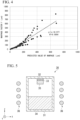
- FIG. 4 is a diagram showing a relationship between a predicted value of the warpage of the SiC substrate and the warpage factor F.
- the warpage factor F ( ⁇ m) was obtained on the basis of the above formula (1).
- the predicted value of the warpage of the SiC substrate was obtained by simulation.
- the simulation was performed using a finite element method simulator ANSYS. It was separately confirmed that the simulation using the finite element method simulator ANSYS matched results of actually manufactured products.
- the predicted value of the warpage is a distance in the thickness direction between the highest point and the lowest point of the first surface 10a and corresponds to Warp.
- the simulation was performed according to the following procedure.
- the physical property values to be set are a thickness of the SiC substrate, a thickness of the surface layer, a Young's modulus, and a Poisson's ratio.
- Various thicknesses and diameters of the SiC substrate were set as shown in Examples described later.
- the SiC substrate was set to have a Young's modulus of 480 GPa and a Poisson's ratio of 0.20.
- the film thickness of the surface layer was 10 ⁇ m.
- the same values as those of the SiC substrate were used for the Young's modulus and the Poisson's ratio of the surface layer.
- a stress distribution of the SiC substrate and the stress of the surface layer were set.
- the stress applied to the SiC substrate was either +60 MPa, +30 MPa, 0 MPa, or -30 MPa. Stress of 60 MPa was applied to the entire surface layer. The simulation was performed under the above conditions to obtain the warpage of the SiC substrate with the surface layer.
- the warpage factor F has a proportional relationship with the predicted value of the warpage obtained from the simulation.
- the warpage factor F reflects an amount of the warpage of the SiC substrate 10. That is, by controlling the warpage factor F, the warpage after the processing processes can be controlled. Further, when the warpage factor F has been obtained, it is possible to easily predict the amount of the warpage after the SiC substrate 10 has passed through the processing process without performing a simulation or the like.
- the SiC substrate 10 is obtained by slicing a SiC ingot.
- the SiC ingot is obtained, for example, by a sublimation method.
- FIG. 5 is a schematic diagram showing a sublimation method, which is an example of a manufacturing device 30 of the SiC ingot.
- a direction orthogonal to a surface of a base 32 is a z direction
- one direction orthogonal to the z direction is an x direction
- a direction orthogonal to the z direction and the x direction is a y direction.
- the sublimation method is a method of disposing a seed crystal 33 made of SiC single crystal on the base 32 disposed in a crucible 31 made of graphite, supplying a sublimation gas sublimated from raw material powder 34 in the crucible 31 to the seed crystal 33 by heating the crucible 31, and growing the seed crystal 33 into a larger SiC ingot 35.
- the heating of the crucible 31 is performed by a coil 36, for example.
- the diameter R of the SiC substrate 10 used to calculate the warpage factor F is a parameter determined by product specifications. For that reason, a desired SiC substrate 10 can be manufactured by controlling the thickness t s of the SiC substrate 10 and the stress S at the first outer circumferential end 1 in accordance with the defined diameter R of the SiC substrate 10.
- the stress applied inside the SiC substrate 10 obtained from the SiC ingot 35 can be controlled.
- a temperature of a central portion and a temperature of an outer circumferential portion of a crystal growth surface are controlled.
- the crystal growth surface is a surface during a growth process of crystal.
- the temperature of the outer circumferential portion is made lower than the temperature of the central portion of the crystal growth surface.
- crystal growth is performed such that a difference in growth rate between a center and an outer circumference in a xy plane becomes 0.001 mm/h or more and 0.05 mm/h or less.
- the growth rate in the center in the xy plane is made slower than the growth rate in the outer circumference.
- the stress S at the first outer circumferential end 1 is compressive stress
- its absolute value can be reduced
- the stress S at the first outer circumferential end 1 is tensile stress
- its absolute value can be increased.
- the growth rate is changed by changing the temperature of the crystal growth surface.
- the temperature of the crystal growth surface can be adjusted by controlling a position of a heating center of the crucible 31 in the z direction heated by the coil 36.
- the position of the heating center of the crucible 31 in the z direction can be changed by changing a position of the coil 36 in the z direction.
- the position of the heating center of the crucible 31 in the z direction and a position of the crystal growth surface in the z direction are controlled to be separated from each other by 0.5 mm/h.
- the position of the heating center of the crucible 31 in the z direction is controlled to be lower (on the raw material powder 34 side) than the position of the crystal growth surface in the z direction.
- the SiC ingot 35 produced under these conditions is processed into the SiC substrate 10.
- the stress applied to the single crystal changes depending on a state of the SiC ingot 35 and a state of the SiC substrate 10.
- a shaping process it is required to reduce the diameter at the time of processing the SiC ingot 35 with a diameter of 180 mm into the SiC substrate 10 with a diameter of 150 mm.
- undulations occur on the surface, and it is required to remove the undulations.
- a portion of the SiC ingot 35 having large stress may be removed or a shape of a crystal lattice plane may be changed, and the stress in the SiC ingot 35 state may be released in the SiC substrate 10 state.
- the SiC substrate 10 is processed such that the stress applied to the single crystal in the SiC ingot 35 state is transferred thereto.
- the SiC ingot 35 After damage-free processing has been performed on one surface of the SiC ingot 35, it is cut with a single wire saw, and the surface subjected to the damage-free processing is sucked to further perform damage-free processing on the cut surface.
- the damage-free processing is, for example, CMP processing.
- CMP processing In this way, by processing the substrate to leave a lattice plane shape of the SiC ingot 35, the stress included in the SiC ingot 35 is transferred to the SiC substrate 10.
- the shaping process for adjusting the diameter the stress at the first outer circumferential end 1 of the SiC substrate 10 can be adjusted.
- the thickness t s of the SiC substrate 10 is determined.
- the thickness t s of the SiC substrate 10 is reduced in order to increase the number of SiC substrates 10 obtained from the SiC ingot 35, production efficiency is improved, but the thickness t s of SiC substrate 10 is designed such that the warpage factor F is within a predetermined value.
- the lower limit value of the thickness t s of the SiC substrate 10 is predicted from the diameter R of the SiC substrate 10 and the stress at the SiC substrate 10 that can be predicted from the SiC ingot state, and the thickness t s of the SiC substrate 10 is set to be thicker than the above thickness.
- the SiC substrate 10 according to the present embodiment having the warpage factor F equal to or less than a specified value can be produced.
- the warpage factor F obtained from the diameter R, the thickness t s , and the stress S of the SiC substrate 10 has a correlation with the amount of the warpage obtained from the simulation in the case in which the processed layer 11 is formed on the SiC substrate 10. Also, the simulation results in the case of forming the processed layer 11 on the SiC substrate 10 have a correlation with actually measured values. That is, by using the warpage factor F obtained from the diameter R, the thickness t s , and the stress S of the SiC substrate 10, the warpage of the SiC substrate 10 after the processing processes can be easily predicted.
- An allowable value of the warpage of the SiC substrate after the processing processes varies depending on specifications of products and processing processes. As described above, if the amount of the warpage of the SiC substrate after the processing processes can be predicted from the values of the diameter R, the thickness t s , and the stress S of the SiC substrate 10 before processing, sorting of the SiC substrate 10 can be performed before it is processed, and probability of producing defective products in the processing processes can be lowered. In addition, by reducing the thickness t s of the SiC substrate 10 within a range in which the warpage does not occur in the processing processes, many SiC substrates 10 can be obtained from the SiC ingot 35, and production efficiency can be improved. The number of the SiC substrates 10 obtained from the SiC ingot 35 is increased, and defects in the processing processes due to the warpage are reduced, so that the cost per SiC substrate 10 can be reduced.
- the warpage when the processed layer was laminated on the surface of the SiC substrate was obtained by simulation.
- the simulation was performed using the finite element method simulator ANSYS. It was separately confirmed that the simulation using the finite element method simulator ANSYS matched results of an actually manufactured product.
- the simulation was performed according to the following procedure.
- the physical property values to be set are the thickness of the SiC substrate, the thickness of the surface layer, the Young's modulus, and the Poisson's ratio.
- the plate thickness of the SiC substrate was set to 350 ⁇ m.
- the diameter of the SiC substrate was set to 75 mm.
- the SiC substrate was set to have a Young's modulus of 480 GPa and a Poisson's ratio of 0.20.
- the film thickness of the surface layer was 0.01 mm.
- the same values as those of the SiC substrate were used for the Young's modulus and the Poisson's ratio of the surface layer.
- the amount of the warpage of the SiC substrate was obtained by changing the thickness of the SiC substrate and the stress applied to the first outer circumferential end of the SiC substrate.
- the stress applied to the first outer circumferential end was obtained in four patterns of -30 MPa (compressive stress), 0 MPa, +30 MPa (tensile stress), and +60 MPa (tensile stress).
- Example 2 is different from Example 1 in that the SiC substrate has a diameter of 100 mm. Other conditions were the same as in Example 1, and the amount of the warpage of the SiC substrate was obtained by simulation.
- Example 3 is different from Example 1 in that the SiC substrate has a diameter of 150 mm. Other conditions were the same as in Example 1, and the amount of the warpage of the SiC substrate was obtained by simulation.
- Example 4 is different from Example 1 in that the SiC substrate has a diameter of 200 mm. Other conditions were the same as in Example 1, and the amount of the warpage of the SiC substrate was obtained by simulation.
- Example 5 is different from Example 1 in that the SiC substrate has a diameter of 250 mm. Other conditions were the same as in Example 1, and the amount of the warpage of the SiC substrate was obtained by simulation.
- Example 6 is different from Example 1 in that the SiC substrate has a diameter of 300 mm. Other conditions were the same as in Example 1, and the amount of the warpage of the SiC substrate was obtained by simulation.
- FIG. 4 shows relationships between results of Examples 1 to 6 and the warpage parameter F. That is, it can be confirmed that there is a correlation between the simulation results of the warpage of the SiC substrate after forming the processed layer and the warpage parameter F of the SiC substrate before forming the processed layer.
Landscapes
- Chemical & Material Sciences (AREA)
- Engineering & Computer Science (AREA)
- Crystallography & Structural Chemistry (AREA)
- Materials Engineering (AREA)
- Metallurgy (AREA)
- Organic Chemistry (AREA)
- Inorganic Chemistry (AREA)
- Crystals, And After-Treatments Of Crystals (AREA)
- Physical Deposition Of Substances That Are Components Of Semiconductor Devices (AREA)
Abstract
Description
- The present invention relates to a SiC substrate and a SiC epitaxial wafer.
- Silicon carbide (SiC) has a dielectric breakdown field that is one order of magnitude larger and a bandgap that is three times larger than silicon (Si). In addition, silicon carbide (SiC) has properties such as a thermal conductivity that is about three times greater than silicon (Si). For that reason, silicon carbide (SiC) is expected to be applied to power devices, high-frequency devices, high-temperature operation devices, and the like. For this reason, in recent years, SiC epitaxial wafers have come to be used for such semiconductor devices.
- A SiC epitaxial wafer is obtained by laminating a SiC epitaxial layer on a surface of a SiC substrate cut out from a SiC ingot. Hereinafter, a substrate before a SiC epitaxial layer is laminated thereon is referred to as a SiC substrate, and a substrate after a SiC epitaxial layer has been laminated thereon is referred to as a SiC epitaxial wafer.
- A SiC substrate before a SiC epitaxial layer is laminated is flat. There are various processing processes before a semiconductor device is manufactured from the SiC substrate. A SiC substrate may warp after processing processes. Processing processes that cause warpage of a SiC substrate include, for example, epitaxial layer deposition, surface polishing, oxide film formation, ion implantation, and the like. Warpage of a SiC substrate adversely affects processes of a semiconductor device. For example, the warpage causes defocus in photolithographic processing. The warpage also causes a decrease in positional accuracy of a wafer during a transfer process.
- On the other hand, as mentioned above, a SiC substrate before processing is flat, and it is difficult to predict the warpage after processing. For example,
Patent Document 1 describes using a difference in wavenumber shift amount of Raman scattered light in order to predict a warpage value of a SiC single crystal product wafer after completion of a polishing process before the polishing process is completed. Patent Document 2 discloses a substrate in which a Raman spectrum is measured in a thickness direction of a substrate and a stress distribution is reduced in the thickness direction. Also, for example, Patent Document 3 describes that warpage of a SiC substrate is reduced by relaxing crystallographic stress. Further, for example, Patent Document 4 describes inhibiting cracks in an ingot by increasing a compressive stress in a circumferential direction of the ingot. -
- [Patent Document 1]
Japanese Unexamined Patent Application, First Publication No. 2015-59073 - [Patent Document 2]
PCT International Publication No. WO 2019/111507 - [Patent Document 3]
United States Patent Application Publication No. 2021/0198804 - [Patent Document 4]
Japanese Unexamined Patent Application, First Publication No. 2007-290880 -
Patent Documents 1 and 2 use a Raman shift to evaluate internal stress of a substrate, but the Raman shift does not include directional information. Further,Patent Documents 1 to 3 describe reducing stress, but warpage of a SiC epitaxial wafer could not be sufficiently inhibited only by reducing stress. Moreover, the stress defined in Patent Document 4 is stress of an ingot, which is different from the stress associated with a SiC substrate. - The present invention has been made in view of the above problems, and an object thereof is to provide a SiC substrate and a SiC epitaxial wafer that are less likely to warp even after processing.
- The present inventors have found a new function (a warpage factor) that correlates with warpage after processing using stress at an outer circumferential portion, a diameter, and a thickness. It has been found that, by inhibiting the warpage factor below a certain value, the warpage after processing can be inhibited and obstruction to device flow can be inhibited. In order to solve the above problems, the present invention provides the following means.
- (1) A SiC substrate according to a first aspect having a warpage factor F of 300 µm or less represented by the following formula (1) obtained from a thickness, a diameter, and a stress at a first outer
circumferential end 10 mm inward from an outer circumferential end in the [11-20] direction from a center thereof. - Here, the formula (1) is expressed as F=K×exp(a+b×ln(σ)+c×ln(R)+d×ln(ts)) ··· (1).
- In the formula (1), K, a, b, c, and d are constants satisfying K=1.3373, a=-11.67123, b=1.4030953, c=1.8050972, and d=-1.585898, σ satisfies σ=60 (MPa)-2/3×S (MPa), S is internal stress in the <1-100> direction, which is the same direction as a circumferential direction of the first outer circumferential end, and in which tensile stress is defined as positive and compressive stress is defined as negative, ts is the thickness (mm), and R is the diameter (mm).
- (2) In the SiC substrate according to the above aspect, the warpage factor F may be 200 µm or less.
- (3) In the SiC substrate according to the above aspect, the warpage factor F may be 100 µm or less.
- (4) In the SiC substrate according to the above aspect, the warpage factor F may be 50 µm or less.
- (5) In the SiC substrate according to the above aspect, the diameter may be 145 mm or more.
- (6) In the SiC substrate according to the above aspect, the diameter may be 195 mm or more.
- (7) In the SiC substrate according to the above aspect, the diameter may be 210 mm or more.
- (8) In the SiC substrate according to the above aspect, the diameter may be 290 mm or more.
- (9) In the SiC substrate according to the above aspect, the thickness may be 800 µm or less.
- (10) In the SiC substrate according to the above aspect, the thickness may be 600 µm or less.
- (11) In the SiC substrate according to the above aspect, the thickness may be 400 µm or less.
- (12) In the SiC substrate according to the above aspect, the thickness may be 300 µm or less.
- (13) A SiC epitaxial wafer according to a second aspect includes the SiC substrate according to the above aspect, and a SiC epitaxial layer laminated on one surface of the SiC substrate.
- The SiC substrate and the SiC epitaxial wafer according to the above aspects are less likely to warp even after processing processes.
-
-
FIG. 1 is a schematic diagram showing warpage of a SiC substrate. -
FIG. 2 is a plan view of the SiC substrate according to the present embodiment. -
FIG. 3 is a schematic diagram showing a method for measuring stress S in a circumferential direction of a first outer circumferential end. -
FIG. 4 is a diagram showing a relationship between a predicted (simulated) value of the warpage of the SiC substrate and a warpage factor. -
FIG. 5 is a schematic diagram showing a sublimation method, which is an example of a manufacturing device of a SiC ingot. -
FIG. 6 shows simulation results of warpage of a SiC substrate in Example 1. -
FIG. 7 shows simulation results of warpage of a SiC substrate in Example 2. -
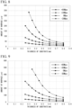
FIG. 8 shows simulation results of warpage of a SiC substrate in Example 3. -
FIG. 9 shows simulation results of warpage of a SiC substrate in Example 4. -
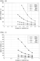
FIG. 10 shows simulation results of warpage of a SiC substrate in Example 5. -
FIG. 11 shows simulation results of warpage of a SiC substrate in Example 6. - A SiC substrate and the like according to the present embodiment will be described in detail below with reference to the drawings as appropriate. In the drawings used in the following description, there are cases in which featured portions are shown enlarged for the sake of convenience in order to make it easier to understand features of the present embodiment, and dimensional ratios and the like of respective constituent elements may be different from actual ones. Materials, dimensions, and the like provided in the following description are exemplary examples, and the present invention is not limited thereto and can be appropriately modified without changing the gist thereof.
- First, warpage of a
SiC substrate 10 will be described.FIG. 1 is a schematic diagram showing the warpage of theSiC substrate 10. - The
SiC substrate 10 before processing is substantially flat. The expression "substantially flat" means that there is no portion that rises significantly when placed on a flat surface. For example, afirst surface 10a and asecond surface 10b of theSiC substrate 10 before processing are substantially parallel to each other. Thefirst surface 10a and thesecond surface 10b are opposite surfaces of theSiC substrate 10. - After processing processes, a processed
layer 11 is formed on thefirst surface 10a of theSiC substrate 10. The processedlayer 11 is formed by, for example, surface treatment, film formation, device formation, or the like. When the processedlayer 11 is formed on one surface of theSiC substrate 10, theSiC substrate 10 may warp. - For example, the processed
layer 11 formed by surface treatment is an affected layer. For example, when thefirst surface 10a is a mirror-ground surface and thesecond surface 10b is a CMP-processed surface, the affected layer is formed on thefirst surface 10a. The Twyman effect occurs in theSiC substrate 10 due to a difference in surface state between thefirst surface 10a and thesecond surface 10b. The Twyman effect is a phenomenon in which, in a case in which there is a difference in residual stress on both surfaces of a substrate, a force acts to compensate for the difference in stress on both surfaces. The Twyman effect may cause theSiC epitaxial wafer 20 to warp. - Also, for example, the processed
layer 11 formed by film formation is an epitaxial layer. The epitaxial layer is deposited on afirst surface 10a of theSiC substrate 10, for example. TheSiC substrate 10 may warp due to a difference in state between thefirst surface 10a on which the epitaxial layer is formed and thesecond surface 10b. - Also, for example, the processed
layer 11 formed by device formation is a device layer. For example, diodes and transistors are formed in the device layer. For example, when ion implantation or the like is performed to form a device in an epitaxial layer, theSiC substrate 10 may warp. This is because a state is different between an ion-implanted surface and a non-ion-implanted surface. - Here, one example of causes of the warpage of the
SiC substrate 10 due to the processing processes has been presented, but the causes of the warpage are not limited thereto, and these causes may affect it in a complex manner. For that reason, it has been difficult to predict a degree of the warpage after the processing processes in the state of theSiC substrate 10. In the SiC substrate according to the present embodiment, the degree of the warpage after the processing processes is defined by a newly defined warpage factor F. -
FIG. 2 is a plan view of theSiC substrate 10 according to the present embodiment. TheSiC substrate 10 is made of SiC. A polytype of theSiC substrate 10 is not particularly limited and may be any of 2H, 3C, 4H, and 6H. TheSiC substrate 10 is, for example, 4H-SiC. The shape of theSiC substrate 10 in a plan view is substantially circular. TheSiC substrate 10 may have an orientation flat OF or a notch for determining a direction of a crystal axis thereof. - The warpage factor F is a parameter obtained from a thickness ts (see
FIG. 1 ), a diameter R, and stress S at a first outercircumferential end 1 of theSiC substrate 10. - The warpage factor F (µm) is represented by the following formula (1).

- In the formula (1), K, a, b, c, and d are constants. They satisfy K=1.3373, a=-11.67123, b=1.4030953, c=1.8050972, and d=-1.585898. σ satisfies σ=60 (MPa)-2/3×S (MPa). S is the stress at the first outer
circumferential end 1. ts is the thickness (mm) of theSiC substrate 10 and R is the diameter (mm) of theSiC substrate 10. - The first outer
circumferential end 1 is located at an outer circumferential portion 2 10 mm inward from an outer circumferential end and is a point located in the [11-20] direction from a center C thereof. The stress S is an internal stress in the <1-100> direction, which is the same direction as a circumferential direction of the first outercircumferential end 1. Also, in the present invention, when the stress S is a tensile stress, it is treated as positive, and when it is a compressive stress, it is treated as negative. At the time of discussing a magnitude of the stress S, the magnitude is defined by an absolute value. - The stress S is calculated as a product of a strain ε and a Young's modulus. The strain ε is obtained by (a0-a)/a0. a0 is a reference lattice constant, a0 is about 3.08 Å in the case of 4H-SiC. a is a lattice constant determined by an X-ray diffraction method (XRD). A direction of the stress S is obtained from a direction of incident X-rays in X-ray diffraction. As the lattice constant a becomes smaller than a reference lattice constant a0, the strain ε increases and the tensile stress increases. As the lattice constant a becomes larger than the reference lattice constant a0, the strain ε increases and the tensile stress increases.
-
FIG. 3 is a schematic diagram showing a method for measuring the stress S in the circumferential direction of the first outercircumferential end 1. The circumferential direction at the first outercircumferential end 1 is a direction orthogonal to a line segment that connects the center C of theSiC substrate 10 to the first outer circumferential end 1 (hereinafter referred to as a first direction). The first direction is the <1-100> direction. In the case of measuring the stress in the circumferential direction at the first outercircumferential end 1, X-rays are radiated in the first direction. By making X-rays incident on theSiC substrate 10 in the circumferential direction, the lattice constant a in the circumferential direction at the first outercircumferential end 1 is obtained. Then, using this lattice constant a, the stress S in the circumferential direction at the first outercircumferential end 1 is obtained from the above formula. In addition, when the actually measured lattice constant a is smaller than the reference lattice constant a0, tensile stress is assumed to be acting, and when the actually measured lattice constant a is greater than the reference lattice constant a0, compressive stress is assumed to be acting. - The warpage factor F is, for example, 300 µm or less, preferably 200 µm or less, more preferably 100 µm or less, and even more preferably 50 µm or less.
- The value of the warpage factor F is satisfied preferably when the diameter of the
SiC substrate 10 is 145 mm or more, more preferably when the diameter is 195 mm or more, even more preferably when the diameter is 210 mm or more, and particularly preferably when the diameter is 290 mm or more. - The value of the warpage factor F is satisfied preferably when the thickness ts of the
SiC substrate 10 is 800 µm or less, more preferably when the thickness ts is 600 µm or less, even more preferably when the thickness ts is 400 µm or less, and particularly preferably when the thickness ts is 300 µm or less. - For example, in a case in which the
SiC substrate 10 has the diameter of 290 mm or more and the thickness of 800 µm or less, the warpage factor F is preferably 300 µm or less, more preferably 200 µm or less, even more preferably 100 µm or less, and particularly preferably 50 µm or less. Also, in a case in which theSiC substrate 10 has the diameter of 290 mm or more and the thickness of 600 µm or less, the warpage factor F is preferably 300 µm or less, more preferably 200 µm or less, even more preferably 100 µm or less, and particularly preferably 50 µm or less. - For example, in a case in which the
SiC substrate 10 has the diameter of 210 mm or more and the thickness of 600 µm or less, the warpage factor F is preferably 300 µm or less, more preferably 200 µm or less, even more preferably 100 µm or less, and particularly preferably 50 µm or less. - For example, in a case in which the
SiC substrate 10 has the diameter of 195 mm or more and the thickness of 600 µm or less, the warpage factor F is preferably 100 µm or less and more preferably 50 µm or less. Also, in a case in which theSiC substrate 10 has the diameter of 195 mm or more and the thickness of 400 µm or less, the warpage factor F is preferably 200 µm or less, more preferably 100 µm or less, and even more preferably 50 µm or less. - For example, in a case in which the
SiC substrate 10 has the diameter of 145 mm or more and the thickness of 300 µm or less, the warpage factor F is preferably 100 µm or less and more preferably 50 µm or less. -
FIG. 4 is a diagram showing a relationship between a predicted value of the warpage of the SiC substrate and the warpage factor F. The warpage factor F (µm) was obtained on the basis of the above formula (1). - The predicted value of the warpage of the SiC substrate was obtained by simulation. The simulation was performed using a finite element method simulator ANSYS. It was separately confirmed that the simulation using the finite element method simulator ANSYS matched results of actually manufactured products. The predicted value of the warpage is a distance in the thickness direction between the highest point and the lowest point of the
first surface 10a and corresponds to Warp. - The simulation was performed according to the following procedure. First, physical property values of the SiC substrate and the surface layer with different stresses were set. The physical property values to be set are a thickness of the SiC substrate, a thickness of the surface layer, a Young's modulus, and a Poisson's ratio. Various thicknesses and diameters of the SiC substrate were set as shown in Examples described later. The SiC substrate was set to have a Young's modulus of 480 GPa and a Poisson's ratio of 0.20. The film thickness of the surface layer was 10 µm. Here, in consideration of a case in which the stress is generated in the surface layer by ion implantation, the same values as those of the SiC substrate were used for the Young's modulus and the Poisson's ratio of the surface layer.
- Next, a stress distribution of the SiC substrate and the stress of the surface layer were set. First, the stress distribution of the SiC substrate was set. The stress applied to the SiC substrate was either +60 MPa, +30 MPa, 0 MPa, or -30 MPa. Stress of 60 MPa was applied to the entire surface layer. The simulation was performed under the above conditions to obtain the warpage of the SiC substrate with the surface layer.
- As shown in
FIG. 4 , the warpage factor F has a proportional relationship with the predicted value of the warpage obtained from the simulation. The warpage factor F reflects an amount of the warpage of theSiC substrate 10. That is, by controlling the warpage factor F, the warpage after the processing processes can be controlled. Further, when the warpage factor F has been obtained, it is possible to easily predict the amount of the warpage after theSiC substrate 10 has passed through the processing process without performing a simulation or the like. - Next, an example of a method for manufacturing the
SiC substrate 10 according to the present embodiment will be described. TheSiC substrate 10 is obtained by slicing a SiC ingot. The SiC ingot is obtained, for example, by a sublimation method. -
FIG. 5 is a schematic diagram showing a sublimation method, which is an example of amanufacturing device 30 of the SiC ingot. InFIG. 5 , a direction orthogonal to a surface of abase 32 is a z direction, one direction orthogonal to the z direction is an x direction, and a direction orthogonal to the z direction and the x direction is a y direction. - The sublimation method is a method of disposing a
seed crystal 33 made of SiC single crystal on the base 32 disposed in acrucible 31 made of graphite, supplying a sublimation gas sublimated fromraw material powder 34 in thecrucible 31 to theseed crystal 33 by heating thecrucible 31, and growing theseed crystal 33 into alarger SiC ingot 35. The heating of thecrucible 31 is performed by acoil 36, for example. - The diameter R of the
SiC substrate 10 used to calculate the warpage factor F is a parameter determined by product specifications. For that reason, a desiredSiC substrate 10 can be manufactured by controlling the thickness ts of theSiC substrate 10 and the stress S at the first outercircumferential end 1 in accordance with the defined diameter R of theSiC substrate 10. - First, by controlling crystal growth conditions in the sublimation method, the stress applied inside the
SiC substrate 10 obtained from theSiC ingot 35 can be controlled. - For example, when the
SiC ingot 35 is c-plane grown, a temperature of a central portion and a temperature of an outer circumferential portion of a crystal growth surface are controlled. The crystal growth surface is a surface during a growth process of crystal. For example, when theSiC ingot 35 is c-plane grown, the temperature of the outer circumferential portion is made lower than the temperature of the central portion of the crystal growth surface. In addition, crystal growth is performed such that a difference in growth rate between a center and an outer circumference in a xy plane becomes 0.001 mm/h or more and 0.05 mm/h or less. Here, the growth rate in the center in the xy plane is made slower than the growth rate in the outer circumference. By performing the crystal growth in this way, in a case in which the stress S at the first outercircumferential end 1 is compressive stress, its absolute value can be reduced, and in a case in which the stress S at the first outercircumferential end 1 is tensile stress, its absolute value can be increased. The growth rate is changed by changing the temperature of the crystal growth surface. - The temperature of the crystal growth surface can be adjusted by controlling a position of a heating center of the
crucible 31 in the z direction heated by thecoil 36. For example, the position of the heating center of thecrucible 31 in the z direction can be changed by changing a position of thecoil 36 in the z direction. The position of the heating center of thecrucible 31 in the z direction and a position of the crystal growth surface in the z direction are controlled to be separated from each other by 0.5 mm/h. Here, the position of the heating center of thecrucible 31 in the z direction is controlled to be lower (on theraw material powder 34 side) than the position of the crystal growth surface in the z direction. - Next, the
SiC ingot 35 produced under these conditions is processed into theSiC substrate 10. In a general processing method, the stress applied to the single crystal changes depending on a state of theSiC ingot 35 and a state of theSiC substrate 10. For example, in a shaping process, it is required to reduce the diameter at the time of processing theSiC ingot 35 with a diameter of 180 mm into theSiC substrate 10 with a diameter of 150 mm. In addition, for example, in a multi-wire cutting process, undulations occur on the surface, and it is required to remove the undulations. By going through such a process, for example, a portion of theSiC ingot 35 having large stress may be removed or a shape of a crystal lattice plane may be changed, and the stress in theSiC ingot 35 state may be released in theSiC substrate 10 state. TheSiC substrate 10 is processed such that the stress applied to the single crystal in theSiC ingot 35 state is transferred thereto. - For example, after damage-free processing has been performed on one surface of the
SiC ingot 35, it is cut with a single wire saw, and the surface subjected to the damage-free processing is sucked to further perform damage-free processing on the cut surface. By performing the damage-free processing on both surfaces of theSiC substrate 10, part of the stress generated in the SiC ingot state is transferred to theSiC substrate 10. The damage-free processing is, for example, CMP processing. In this way, by processing the substrate to leave a lattice plane shape of theSiC ingot 35, the stress included in theSiC ingot 35 is transferred to theSiC substrate 10. After that, by performing the shaping process for adjusting the diameter, the stress at the first outercircumferential end 1 of theSiC substrate 10 can be adjusted. - Also, when the
SiC ingot 35 is processed into theSiC substrate 10, the thickness ts of theSiC substrate 10 is determined. When the thickness ts of theSiC substrate 10 is reduced in order to increase the number ofSiC substrates 10 obtained from theSiC ingot 35, production efficiency is improved, but the thickness ts ofSiC substrate 10 is designed such that the warpage factor F is within a predetermined value. The lower limit value of the thickness ts of theSiC substrate 10 is predicted from the diameter R of theSiC substrate 10 and the stress at theSiC substrate 10 that can be predicted from the SiC ingot state, and the thickness ts of theSiC substrate 10 is set to be thicker than the above thickness. - In this way, by controlling the thickness ts of the
SiC substrate 10 and the stress S at the first outercircumferential end 1 in accordance with the diameter R of theSiC substrate 10 specified by the specifications, theSiC substrate 10 according to the present embodiment having the warpage factor F equal to or less than a specified value can be produced. - As described above, the warpage factor F obtained from the diameter R, the thickness ts, and the stress S of the
SiC substrate 10 has a correlation with the amount of the warpage obtained from the simulation in the case in which the processedlayer 11 is formed on theSiC substrate 10. Also, the simulation results in the case of forming the processedlayer 11 on theSiC substrate 10 have a correlation with actually measured values. That is, by using the warpage factor F obtained from the diameter R, the thickness ts, and the stress S of theSiC substrate 10, the warpage of theSiC substrate 10 after the processing processes can be easily predicted. - An allowable value of the warpage of the SiC substrate after the processing processes varies depending on specifications of products and processing processes. As described above, if the amount of the warpage of the SiC substrate after the processing processes can be predicted from the values of the diameter R, the thickness ts, and the stress S of the
SiC substrate 10 before processing, sorting of theSiC substrate 10 can be performed before it is processed, and probability of producing defective products in the processing processes can be lowered. In addition, by reducing the thickness ts of theSiC substrate 10 within a range in which the warpage does not occur in the processing processes,many SiC substrates 10 can be obtained from theSiC ingot 35, and production efficiency can be improved. The number of theSiC substrates 10 obtained from theSiC ingot 35 is increased, and defects in the processing processes due to the warpage are reduced, so that the cost perSiC substrate 10 can be reduced. - Although the preferred embodiments of the present invention have been described in detail above, the present invention is not limited to the specific embodiments, and various modifications and changes are possible within the scope of the gist of the present invention described in the claims.
- The warpage when the processed layer was laminated on the surface of the SiC substrate was obtained by simulation. The simulation was performed using the finite element method simulator ANSYS. It was separately confirmed that the simulation using the finite element method simulator ANSYS matched results of an actually manufactured product.
- The simulation was performed according to the following procedure. First, physical property values of the SiC substrate and the surface layer with different stresses were set. The physical property values to be set are the thickness of the SiC substrate, the thickness of the surface layer, the Young's modulus, and the Poisson's ratio. The plate thickness of the SiC substrate was set to 350 µm. The diameter of the SiC substrate was set to 75 mm. The SiC substrate was set to have a Young's modulus of 480 GPa and a Poisson's ratio of 0.20. The film thickness of the surface layer was 0.01 mm. In consideration of the case in which stress is generated in the processed layer by ion implantation, the same values as those of the SiC substrate were used for the Young's modulus and the Poisson's ratio of the surface layer.
- Then, the amount of the warpage of the SiC substrate was obtained by changing the thickness of the SiC substrate and the stress applied to the first outer circumferential end of the SiC substrate. The stress applied to the first outer circumferential end was obtained in four patterns of -30 MPa (compressive stress), 0 MPa, +30 MPa (tensile stress), and +60 MPa (tensile stress).
- Example 2 is different from Example 1 in that the SiC substrate has a diameter of 100 mm. Other conditions were the same as in Example 1, and the amount of the warpage of the SiC substrate was obtained by simulation.
- Example 3 is different from Example 1 in that the SiC substrate has a diameter of 150 mm. Other conditions were the same as in Example 1, and the amount of the warpage of the SiC substrate was obtained by simulation.
- Example 4 is different from Example 1 in that the SiC substrate has a diameter of 200 mm. Other conditions were the same as in Example 1, and the amount of the warpage of the SiC substrate was obtained by simulation.
- Example 5 is different from Example 1 in that the SiC substrate has a diameter of 250 mm. Other conditions were the same as in Example 1, and the amount of the warpage of the SiC substrate was obtained by simulation.
- Example 6 is different from Example 1 in that the SiC substrate has a diameter of 300 mm. Other conditions were the same as in Example 1, and the amount of the warpage of the SiC substrate was obtained by simulation.
-
FIG. 4 shows relationships between results of Examples 1 to 6 and the warpage parameter F. That is, it can be confirmed that there is a correlation between the simulation results of the warpage of the SiC substrate after forming the processed layer and the warpage parameter F of the SiC substrate before forming the processed layer. - Also, from the results of Examples 1 to 6, it can be seen that, as the diameter R of the SiC substrate becomes larger, the amount of the warpage of the SiC substrate after processing increases. In addition, from the results of Examples 1 to 6, it can be seen that, as the thickness ts of the SiC substrate becomes thinner, the amount of the warpage of the SiC substrate after processing increases. Further, from the results of Examples 1 to 6, it can be seen that, in a case in which the stress applied to the first outer circumferential end of the SiC substrate is compressive stress, as its absolute value becomes smaller, the amount of the warpage of the SiC substrate after processing increases, and in a case in which the stress applied to the first outer circumferential end of the SiC substrate is tensile stress, as its absolute value becomes larger, the amount of the warpage of the SiC substrate after processing increases. This result matches the fact that parameters for determining the warpage parameter F are obtained from the diameter R, the thickness ts, and the stress S of the SiC substrate.
-
- 1 First outer circumferential end
- 2 Outer circumferential portion
- 10 SiC substrate
- 10a First surface
- 10b Second surface
- 11 Processed layer
- C Center
- R Diameter
- S Stress
Claims (13)
- A SiC substrate having a warpage factor F of 300 µm or less represented by the following formula (1) obtained from a thickness, a diameter, and a stress at a first outer circumferential end 10 mm inward from an outer circumferential end in the [11-20] direction from a center thereof,
 where K, a, b, c, and d are constants satisfying K=1.3373, a=-11.67123, b=1 .4030953, c=1.8050972, and d=-1.585898,σ satisfies σ=60 (MPa)-2/3×S (MPa),S is internal stress in the <1-100> direction, which is the same direction as a circumferential direction of the first outer circumferential end, and in which tensile stress is defined as positive and compressive stress is defined as negative,ts is the thickness (mm), andR is the diameter (mm).
 - The SiC substrate according to claim 1,
wherein the warpage factor F is 200 µm or less. - The SiC substrate according to claim 1 or 2,
wherein the warpage factor F is 100 µm or less. - The SiC substrate according to any one of claims 1 to 3,
wherein the warpage factor F is 50 µm or less. - The SiC substrate according to any one of claims 1 to 4,
wherein the diameter is 145 mm or more. - The SiC substrate according to any one of claims 1 to 5,
wherein the diameter is 195 mm or more. - The SiC substrate according to any one of claims 1 to 6,
wherein the diameter is 210 mm or more. - The SiC substrate according to any one of claims 1 to 7,
wherein the diameter is 290 mm or more. - The SiC substrate according to any one of claims 1 to 8,
wherein the thickness is 800 µm or less. - The SiC substrate according to any one of claims 1 to 9,
wherein the thickness is 600 µm or less. - The SiC substrate according to any one of claims 1 to 10,
wherein the thickness is 400 µm or less. - The SiC substrate according to any one of claims 1 to 11,
wherein the thickness is 300 µm or less. - A SiC epitaxial wafer comprising the SiC substrate according to any one of claims 1 to 12, and a SiC epitaxial layer laminated on one surface of the SiC substrate.
Applications Claiming Priority (1)
| Application Number | Priority Date | Filing Date | Title |
|---|---|---|---|
| JP2022089095A JP7132454B1 (en) | 2022-05-31 | 2022-05-31 | SiC substrate and SiC epitaxial wafer |
Publications (1)
| Publication Number | Publication Date |
|---|---|
| EP4286568A1 true EP4286568A1 (en) | 2023-12-06 |
Family
ID=83188031
Family Applications (1)
| Application Number | Title | Priority Date | Filing Date |
|---|---|---|---|
| EP23175775.8A Pending EP4286568A1 (en) | 2022-05-31 | 2023-05-26 | Sic substrate and sic epitaxial wafer |
Country Status (6)
| Country | Link |
|---|---|
| US (2) | US12132085B2 (en) |
| EP (1) | EP4286568A1 (en) |
| JP (1) | JP7132454B1 (en) |
| KR (1) | KR102606186B1 (en) |
| CN (1) | CN117144468A (en) |
| TW (1) | TWI831700B (en) |
Families Citing this family (1)
| Publication number | Priority date | Publication date | Assignee | Title |
|---|---|---|---|---|
| JP7268784B1 (en) | 2022-05-31 | 2023-05-08 | 株式会社レゾナック | SiC substrate and SiC epitaxial wafer |
Citations (6)
| Publication number | Priority date | Publication date | Assignee | Title |
|---|---|---|---|---|
| JP2007290880A (en) | 2006-04-21 | 2007-11-08 | Nippon Steel Corp | Silicon carbide single crystal ingot and method for producing the same |
| JP2011219296A (en) * | 2010-04-07 | 2011-11-04 | Nippon Steel Corp | Silicon carbide single crystal wafer |
| US20130009170A1 (en) * | 2007-09-12 | 2013-01-10 | Showa Denko K.K. | EPITAXIAL SiC SINGLE CRYSTAL SUBSTRATE AND METHOD OF MANUFACTURE OF EPITAXIAL SiC SINGLE CRYSTAL SUBSTRATE |
| JP2015059073A (en) | 2013-09-20 | 2015-03-30 | 新日鉄住金マテリアルズ株式会社 | Internal stress evaluation method of silicon carbide single crystal wafer, and prediction method of warp of silicon carbide single crystal wafer |
| WO2019111507A1 (en) | 2017-12-08 | 2019-06-13 | 住友電気工業株式会社 | Silicon carbide substrate |
| US20210198804A1 (en) | 2019-12-27 | 2021-07-01 | Cree, Inc. | Large diameter silicon carbide wafers |
Family Cites Families (10)
| Publication number | Priority date | Publication date | Assignee | Title |
|---|---|---|---|---|
| JP5912173B2 (en) * | 2011-05-13 | 2016-04-27 | エルジー エレクトロニクス インコーポレイティド | Channel estimation method based on CSI-RS in wireless communication system and apparatus therefor |
| JP6269854B2 (en) * | 2014-10-31 | 2018-01-31 | 富士電機株式会社 | Method for growing silicon carbide epitaxial film |
| JP6598150B2 (en) * | 2015-07-24 | 2019-10-30 | 昭和電工株式会社 | Method for producing single crystal SiC substrate |
| JP6579889B2 (en) | 2015-09-29 | 2019-09-25 | 昭和電工株式会社 | Method for manufacturing silicon carbide single crystal substrate |
| JP6981505B2 (en) * | 2015-10-15 | 2021-12-15 | 住友電気工業株式会社 | Method for manufacturing silicon carbide epitaxial substrate |
| JP7422479B2 (en) * | 2017-12-22 | 2024-01-26 | 株式会社レゾナック | SiC ingot and method for producing SiC ingot |
| JP2019112261A (en) * | 2017-12-22 | 2019-07-11 | 昭和電工株式会社 | METHOD FOR PROCESSING SiC SINGLE CRYSTAL AND METHOD FOR MANUFACTURING SiC INGOT |
| US10879359B2 (en) * | 2018-03-02 | 2020-12-29 | National Institute Of Advanced Industrial Science And Technology | Silicon carbide epitaxial wafer having a thick silicon carbide layer with small wrapage and manufacturing method thereof |
| JP7190894B2 (en) * | 2018-12-21 | 2022-12-16 | 昭和電工株式会社 | SiC chemical vapor deposition equipment |
| JP7400451B2 (en) | 2019-12-25 | 2023-12-19 | 株式会社レゾナック | Method for manufacturing SiC single crystal |
-
2022
- 2022-05-31 JP JP2022089095A patent/JP7132454B1/en active Active
-
2023
- 2023-02-27 US US18/114,632 patent/US12132085B2/en active Active
- 2023-02-28 CN CN202310173851.5A patent/CN117144468A/en active Pending
- 2023-05-26 EP EP23175775.8A patent/EP4286568A1/en active Pending
- 2023-05-26 KR KR1020230068128A patent/KR102606186B1/en active Active
- 2023-05-29 TW TW112119937A patent/TWI831700B/en active
-
2024
- 2024-09-25 US US18/896,176 patent/US20250015139A1/en active Pending
Patent Citations (7)
| Publication number | Priority date | Publication date | Assignee | Title |
|---|---|---|---|---|
| JP2007290880A (en) | 2006-04-21 | 2007-11-08 | Nippon Steel Corp | Silicon carbide single crystal ingot and method for producing the same |
| US20130009170A1 (en) * | 2007-09-12 | 2013-01-10 | Showa Denko K.K. | EPITAXIAL SiC SINGLE CRYSTAL SUBSTRATE AND METHOD OF MANUFACTURE OF EPITAXIAL SiC SINGLE CRYSTAL SUBSTRATE |
| JP2011219296A (en) * | 2010-04-07 | 2011-11-04 | Nippon Steel Corp | Silicon carbide single crystal wafer |
| JP2015059073A (en) | 2013-09-20 | 2015-03-30 | 新日鉄住金マテリアルズ株式会社 | Internal stress evaluation method of silicon carbide single crystal wafer, and prediction method of warp of silicon carbide single crystal wafer |
| US20160231256A1 (en) * | 2013-09-20 | 2016-08-11 | Nippon Steel & Sumikin Materials Co., Ltd. | Method for evaluating internal stress of silicon carbide monocrystalline wafer and method for predicting warpage in silicone carbide monocrystalline wafer |
| WO2019111507A1 (en) | 2017-12-08 | 2019-06-13 | 住友電気工業株式会社 | Silicon carbide substrate |
| US20210198804A1 (en) | 2019-12-27 | 2021-07-01 | Cree, Inc. | Large diameter silicon carbide wafers |
Also Published As
| Publication number | Publication date |
|---|---|
| KR102606186B1 (en) | 2023-11-29 |
| JP7132454B1 (en) | 2022-09-06 |
| US20250015139A1 (en) | 2025-01-09 |
| TWI831700B (en) | 2024-02-01 |
| CN117144468A (en) | 2023-12-01 |
| TW202400860A (en) | 2024-01-01 |
| US20230387214A1 (en) | 2023-11-30 |
| JP2023176676A (en) | 2023-12-13 |
| US12132085B2 (en) | 2024-10-29 |
Similar Documents
| Publication | Publication Date | Title |
|---|---|---|
| JP6916835B2 (en) | Chamfering Silicon Carbide Substrate and Chamfering Method | |
| CN103476975A (en) | Silicon carbide substrate, silicon carbide ingot and manufacturing methods therefor | |
| CN109957840B (en) | SiC ingot and method for producing SiC ingot | |
| US12540419B2 (en) | SiC epitaxial wafer | |
| CN112567077A (en) | SiC single crystal, method for producing SiC ingot, and method for producing SiC wafer | |
| US20250015139A1 (en) | SiC SUBSTRATE AND SiC EPITAXIAL WAFER | |
| JP7216244B1 (en) | Semiconductor device manufacturing method | |
| US20260132545A1 (en) | SiC EPITAXIAL WAFER | |
| KR102925744B1 (en) | SiC SUBSTRATE AND SiC EPITAXIAL WAFER | |
| KR102834709B1 (en) | SiC EPITAXIAL WAFER | |
| EP4527992A2 (en) | Sic single crystal boule, manufacturing method of sic single crystal boule, and manufacturing method of sic substrate | |
| JP2026511623A (en) | Multilayer substrate wafer having radially grown substrates |
Legal Events
| Date | Code | Title | Description |
|---|---|---|---|
| PUAI | Public reference made under article 153(3) epc to a published international application that has entered the european phase |
Free format text: ORIGINAL CODE: 0009012 |
|
| STAA | Information on the status of an ep patent application or granted ep patent |
Free format text: STATUS: REQUEST FOR EXAMINATION WAS MADE |
|
| 17P | Request for examination filed |
Effective date: 20230616 |
|
| AK | Designated contracting states |
Kind code of ref document: A1 Designated state(s): AL AT BE BG CH CY CZ DE DK EE ES FI FR GB GR HR HU IE IS IT LI LT LU LV MC ME MK MT NL NO PL PT RO RS SE SI SK SM TR |
|
| RAP3 | Party data changed (applicant data changed or rights of an application transferred) |
Owner name: RESONAC CORPORATION |
|
| RBV | Designated contracting states (corrected) |
Designated state(s): AL AT BE BG CH CY CZ DE DK EE ES FI FR GB GR HR HU IE IS IT LI LT LU LV MC ME MK MT NL NO PL PT RO RS SE SI SK SM TR |