EP4284495B1 - Durchführungskopfanordnung und vorrichtung damit - Google Patents
Durchführungskopfanordnung und vorrichtung damit Download PDFInfo
- Publication number
- EP4284495B1 EP4284495B1 EP22704698.4A EP22704698A EP4284495B1 EP 4284495 B1 EP4284495 B1 EP 4284495B1 EP 22704698 A EP22704698 A EP 22704698A EP 4284495 B1 EP4284495 B1 EP 4284495B1
- Authority
- EP
- European Patent Office
- Prior art keywords
- header
- disposed
- conductive
- electronic
- feedthrough
- Prior art date
- Legal status (The legal status is an assumption and is not a legal conclusion. Google has not performed a legal analysis and makes no representation as to the accuracy of the status listed.)
- Active
Links
Images





Classifications
-
- A—HUMAN NECESSITIES
- A61—MEDICAL OR VETERINARY SCIENCE; HYGIENE
- A61N—ELECTROTHERAPY; MAGNETOTHERAPY; RADIATION THERAPY; ULTRASOUND THERAPY
- A61N1/00—Electrotherapy; Circuits therefor
- A61N1/18—Applying electric currents by contact electrodes
- A61N1/32—Applying electric currents by contact electrodes alternating or intermittent currents
- A61N1/36—Applying electric currents by contact electrodes alternating or intermittent currents for stimulation
- A61N1/372—Arrangements in connection with the implantation of stimulators
- A61N1/375—Constructional arrangements, e.g. casings
- A61N1/3752—Details of casing-lead connections
- A61N1/3754—Feedthroughs
-
- A—HUMAN NECESSITIES
- A61—MEDICAL OR VETERINARY SCIENCE; HYGIENE
- A61N—ELECTROTHERAPY; MAGNETOTHERAPY; RADIATION THERAPY; ULTRASOUND THERAPY
- A61N1/00—Electrotherapy; Circuits therefor
- A61N1/18—Applying electric currents by contact electrodes
- A61N1/32—Applying electric currents by contact electrodes alternating or intermittent currents
- A61N1/36—Applying electric currents by contact electrodes alternating or intermittent currents for stimulation
- A61N1/372—Arrangements in connection with the implantation of stimulators
- A61N1/375—Constructional arrangements, e.g. casings
- A61N1/3756—Casings with electrodes thereon, e.g. leadless stimulators
-
- A—HUMAN NECESSITIES
- A61—MEDICAL OR VETERINARY SCIENCE; HYGIENE
- A61N—ELECTROTHERAPY; MAGNETOTHERAPY; RADIATION THERAPY; ULTRASOUND THERAPY
- A61N1/00—Electrotherapy; Circuits therefor
- A61N1/18—Applying electric currents by contact electrodes
- A61N1/32—Applying electric currents by contact electrodes alternating or intermittent currents
- A61N1/36—Applying electric currents by contact electrodes alternating or intermittent currents for stimulation
- A61N1/372—Arrangements in connection with the implantation of stimulators
- A61N1/375—Constructional arrangements, e.g. casings
- A61N1/3758—Packaging of the components within the casing
-
- H—ELECTRICITY
- H01—ELECTRIC ELEMENTS
- H01R—ELECTRICALLY-CONDUCTIVE CONNECTIONS; STRUCTURAL ASSOCIATIONS OF A PLURALITY OF MUTUALLY-INSULATED ELECTRICAL CONNECTING ELEMENTS; COUPLING DEVICES; CURRENT COLLECTORS
- H01R12/00—Structural associations of a plurality of mutually-insulated electrical connecting elements, specially adapted for printed circuits, e.g. printed circuit boards [PCB], flat or ribbon cables, or like generally planar structures, e.g. terminal strips, terminal blocks; Coupling devices specially adapted for printed circuits, flat or ribbon cables, or like generally planar structures; Terminals specially adapted for contact with, or insertion into, printed circuits, flat or ribbon cables, or like generally planar structures
- H01R12/50—Fixed connections
- H01R12/51—Fixed connections for rigid printed circuits or like structures
- H01R12/52—Fixed connections for rigid printed circuits or like structures connecting to other rigid printed circuits or like structures
-
- H—ELECTRICITY
- H01—ELECTRIC ELEMENTS
- H01R—ELECTRICALLY-CONDUCTIVE CONNECTIONS; STRUCTURAL ASSOCIATIONS OF A PLURALITY OF MUTUALLY-INSULATED ELECTRICAL CONNECTING ELEMENTS; COUPLING DEVICES; CURRENT COLLECTORS
- H01R43/00—Apparatus or processes specially adapted for manufacturing, assembling, maintaining, or repairing of line connectors or current collectors or for joining electric conductors
- H01R43/20—Apparatus or processes specially adapted for manufacturing, assembling, maintaining, or repairing of line connectors or current collectors or for joining electric conductors for assembling or disassembling contact members with insulating base, case or sleeve
- H01R43/205—Apparatus or processes specially adapted for manufacturing, assembling, maintaining, or repairing of line connectors or current collectors or for joining electric conductors for assembling or disassembling contact members with insulating base, case or sleeve with a panel or printed circuit board
-
- A—HUMAN NECESSITIES
- A61—MEDICAL OR VETERINARY SCIENCE; HYGIENE
- A61N—ELECTROTHERAPY; MAGNETOTHERAPY; RADIATION THERAPY; ULTRASOUND THERAPY
- A61N1/00—Electrotherapy; Circuits therefor
- A61N1/02—Details
- A61N1/04—Electrodes
- A61N1/05—Electrodes for implantation or insertion into the body, e.g. heart electrode
- A61N1/056—Transvascular endocardial electrode systems
- A61N1/0565—Electrode heads
-
- A—HUMAN NECESSITIES
- A61—MEDICAL OR VETERINARY SCIENCE; HYGIENE
- A61N—ELECTROTHERAPY; MAGNETOTHERAPY; RADIATION THERAPY; ULTRASOUND THERAPY
- A61N1/00—Electrotherapy; Circuits therefor
- A61N1/02—Details
- A61N1/04—Electrodes
- A61N1/05—Electrodes for implantation or insertion into the body, e.g. heart electrode
- A61N1/056—Transvascular endocardial electrode systems
- A61N1/057—Anchoring means; Means for fixing the head inside the heart
-
- A—HUMAN NECESSITIES
- A61—MEDICAL OR VETERINARY SCIENCE; HYGIENE
- A61N—ELECTROTHERAPY; MAGNETOTHERAPY; RADIATION THERAPY; ULTRASOUND THERAPY
- A61N1/00—Electrotherapy; Circuits therefor
- A61N1/18—Applying electric currents by contact electrodes
- A61N1/32—Applying electric currents by contact electrodes alternating or intermittent currents
- A61N1/36—Applying electric currents by contact electrodes alternating or intermittent currents for stimulation
- A61N1/362—Heart stimulators
-
- A—HUMAN NECESSITIES
- A61—MEDICAL OR VETERINARY SCIENCE; HYGIENE
- A61N—ELECTROTHERAPY; MAGNETOTHERAPY; RADIATION THERAPY; ULTRASOUND THERAPY
- A61N1/00—Electrotherapy; Circuits therefor
- A61N1/18—Applying electric currents by contact electrodes
- A61N1/32—Applying electric currents by contact electrodes alternating or intermittent currents
- A61N1/36—Applying electric currents by contact electrodes alternating or intermittent currents for stimulation
- A61N1/372—Arrangements in connection with the implantation of stimulators
- A61N1/375—Constructional arrangements, e.g. casings
- A61N1/37512—Pacemakers
-
- A—HUMAN NECESSITIES
- A61—MEDICAL OR VETERINARY SCIENCE; HYGIENE
- A61N—ELECTROTHERAPY; MAGNETOTHERAPY; RADIATION THERAPY; ULTRASOUND THERAPY
- A61N1/00—Electrotherapy; Circuits therefor
- A61N1/18—Applying electric currents by contact electrodes
- A61N1/32—Applying electric currents by contact electrodes alternating or intermittent currents
- A61N1/38—Applying electric currents by contact electrodes alternating or intermittent currents for producing shock effects
- A61N1/39—Heart defibrillators
- A61N1/3956—Implantable devices for applying electric shocks to the heart, e.g. for cardioversion
- A61N1/3962—Implantable devices for applying electric shocks to the heart, e.g. for cardioversion in combination with another heart therapy
- A61N1/39622—Pacing therapy
Definitions
- This disclosure generally relates to a feedthrough header assembly and in particular an implantable medical device that includes the feedthrough header assembly.
- US 2020/155860 A1 relates to a biostimulator having a flexible circuit assembly.
- aspects of this disclosure relate to an electronics module that includes a feedthrough header assembly.
- the assembly includes a conductive header having a conductive inner surface, an outer surface, and a contact disposed on the inner surface and electrically connected to the header; and a feedthrough pin disposed within a via that extends through the header between the inner surface and the outer surface of the header.
- the feedthrough pin is electrically isolated from the header and includes a first end adjacent to the inner surface of the header and a second end adjacent to the outer surface of the header.
- the electronics module further includes an electronic layer having a substrate and an electronic component disposed on or within the substrate. The electronic component is electrically connected to the contact of the conductive header such that the electronic component is electrically connected to the header.
- a major surface of the substrate of the electronic layer faces the conductive inner surface of the header without any intervening nonconductive layers disposed between the major surface of the substrate and the conductive inner surface of the header.
- aspects of this disclosure relate to a method that includes disposing a feedthrough pin through a via of a conductive header, where a first end of the feedthrough pin is adjacent to a conductive inner surface of the header and a second end of the feedthrough pin is adjacent to an outer surface of the header.
- the method further includes disposing a contact on the inner surface of the header such that it is electrically connected to the header; and electrically connecting an electronic component of an electronic layer to the contact such that the electronic component is electrically connected to the header.
- the electronic component is disposed on or within a substrate of the electronic component. Further, a major surface of the substrate of the electronic layer faces the conductive inner surface of the header without any intervening nonconductive layers disposed between the major surface of the substrate and the conductive inner surface of the header.
- One or more embodiments of the present disclosure can provide a feedthrough header assembly that includes a feedthrough pin that can be connected to an electronics module disposed within a housing of a device, where the feedthrough pin is electrically connected to the module in a reliable manner while efficiently utilizing space within the housing.
- the feedthrough header assembly can be a solderable component or subassembly that is compatible with various standard surface mount processing and connects to an integrated circuit or die stack in a reliable and volumetrically efficient manner.
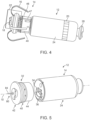
- FIG. 1 is a schematic view of one embodiment of an implantable medical device 12 (IMD) disposed within a body of a patient 2.
- the IMD 12 can include any suitable medical device, e.g., a pacing device, pressure sensing device, cardiac monitor, other physiologic sensor, etc.
- the IMD 12 can include an arrangement of an electronics module and a feedthrough header assembly as is further described herein.
- IMD 12 can be, for example, an implantable leadless pacing device that is configured for implantation entirely within one of the chambers of a heart 4 and that provides electrical signals to the heart beneath a sternum 3 via electrodes carried on the housing of the pacing device.
- fixation elements can secure the IMD 12 to the cardiac tissue and retain an electrode (e.g., a cathode or an anode) in contact with the cardiac tissue.
- IMD 12 can be implanted at or proximate to the apex of the heart.
- a pacing device may be implanted at other ventricular locations, e.g., on the free-wall or septum, an atrial location, or any location on or within the heart 4.
- the housing 14 of the IMD 12 can include any suitable dimensions and take any suitable shape or shapes.
- the housing 14 extends between a first end 6 and a second end 8 along a longitudinal axis 10.
- the housing 14 can have a cylindrical (e.g., pill-shaped) form factor.
- the housing 14 includes an elongated tubular housing. Further, the housing 14 can include any suitable material or materials as is further described herein.
- the IMD 12 includes a plurality of fixation tines 16 that are adapted to anchor the device to tissue
- the device can be fixed to tissue using other types of fixation mechanisms, such as, but not limited to, barbs, coils, and the like.
- the housing 14 can also house a memory that includes instructions that, when executed by processing circuitry housed within housing, cause the IMD 12 to perform various functions attributed to the device herein.
- the housing 14 can house communication circuitry that enables the IMD 12 to communicate with other electronic devices, such as a medical device programmer.
- the housing 14 can house an antenna for wireless communication.
- the housing 14 can also house a power source, such as a battery.
- the housing 14 can be hermetically or near-hermetically sealed using any suitable technique or techniques to help prevent fluid ingress into housing.
- one or more portions of the housing 14 can be hermetically sealed together utilizing one or more laser diffusion bonding techniques described in co-owned U.S. Patent No. 10,124,559 B2 , entitled KINETICALLY LIMITED NANOSCALE DIFFUSION BOND STRUCTURES AND METHODS.
- Electrode 20 can be a portion of housing 14, e.g., second portion 24, that does not include such insulative material. Electrode 20 can be most or all of housing 14, but most of the housing (other than electrode 20) can be covered with an insulative coating. In one or more embodiments, electrode 20 may be coated with materials to promote conduction. In one or more embodiments, electrode 20 can be part of a separate ring portion of housing 14 that is conductive. Electrodes 18, 20, which may include conductive portion(s) of the first portion 22 of housing 14, can be electrically connected to at least some electronics of pacing device 12 (e.g., sensing circuitry, electrical stimulation circuitry, or both).
- pacing device 12 e.g., sensing circuitry, electrical stimulation circuitry, or both.
- the housing 14 can include an end cap 26 that can house or enclose a feedthrough header assembly (e.g., feedthrough header assembly 42 of FIG. 3 ) to electrically connect the electrode 18 to the electronics within the housing 14 while electrically isolating the electrode from the housing 14, e.g., including electrode 20 or other conductive portions of the housing.
- a feedthrough header assembly e.g., feedthrough header assembly 42 of FIG. 3
- the housing 14 includes the first portion 22 and the second portion 24.
- the first portion 22 can be disposed adjacent to the first end 6 of the housing 14, and the second portion 24 can be disposed adjacent to the second end 8 of the housing.
- the term "adjacent to the first end” means that an element or component is disposed closer to the first end 6 of the housing 14 than to the second end 8 of the housing.
- the term "adjacent to the second end” means that an element or component is disposed closer to the second end 8 of the housing 14 than to the first end 6 of the housing.
- the electromagnetic radiation can include laser light that can include any suitable wavelength or range of wavelengths.
- the laser light can include light having a wavelength of at least 200 nm.
- the laser light can include a wavelength of no greater than 10,000 nm.
- laser light can include UV light, visible light, IR light, and combinations thereof.
- a UV laser can be utilized to provide light having a wavelength of about 350 nm and a pulse width of about 30 ns.
- the materials for the first and second portions 22, 24 of the housing 14, and the power level and wavelength of the light used may be selected such that the light may not directly damage, ablate, warp, or cut the housing, and such that the first and second portions of the housing retain their bulk properties.
- the laser may provide light that has a narrow range of wavelengths
- the laser may represent one or more devices that emit light having a wider range of wavelengths than a single typical laser.
- a wide variety of devices may be used to emit light having a narrow or wide range of wavelengths.
- the laser may include one or more laser devices including diode and fiber lasers.
- Laser sources may also include, e.g., TI sapphire, argon ion, Nd:YAG, XeF, HeNe, Dye, GaAs/AlGaAs, CO 2 , Alexandrite, InGaAs, InGaAsP, Nd:glass, Yb:YAG, or Yb fiber lasers.
- the laser device may also include one of continuous wave, modulated, or pulsed modes. Accordingly, a wide variety of laser devices may be used in the bonding process.
- a power level of the laser may be set to approximately 1 W, distributed across the approximate focused beam diameter of 10 ⁇ m, with a top hat or Gaussian spatial energy profile.
- the IMD 12 can also include a flange 28 connected to the second portion 24 of the housing 14 at the second end 8 of the housing that defines an opening.
- the flange 28 can enable medical instruments to attach to the IMD 12, e.g., for delivery and/or extraction of the device.
- a tether that extends through a catheter inserted into the heart 4 ( FIG. 1 ) can be attached to the flange 28 and/or threaded through the opening to implant or extract the IMD 12.
- FIG. 3 is a schematic block diagram of one embodiment of the IMD 12 including a power source 30 (e.g., battery), an electronics module 32, and an electrical contact assembly 34.
- a power source 30 e.g., battery
- an electronics module 32 e.g., an electrical contact assembly 34.
- an electrical contact assembly 34 e.g., an electrical contact assembly 34.
- the IMD of FIG. 3 is described as IMD 12, the structures shown in FIG. 3 can also be used in other implantable or external medical devices, such as cardioverter-defibrillators, physiological monitors, or neurostimulators, or any other electronic devices.
- the housing 14 includes the first and second portions 22, 24 and a side wall 36 disposed within the housing between the battery 30 and the electrical contact assembly 34.
- the side wall 36 can be disposed within the first and second housing portions 22, 24 or at the boundary of first and second housing portions.
- the first and second housing portions 22, 24 are common with a ground terminal of battery 30.
- one or both of the first and second housing portions 22, 24 is non-conductive.
- first housing portion 22 can be formed of a non-conductive material, such as sapphire, which may allow easier transmission of electromagnetic signals into and out of the housing 14 than a metal or other conductive material would allow.
- the side wall 36 extends across housing 14 between the battery 30 on one side and electrical contact assembly 34 on the other side.
- the side wall 36 can include at least one feedthrough (not shown) to allow for electrical connection between the battery 30 and the electronics module 32.
- feedthrough header assembly 42 can also include at least one feedthrough to allow for an electrical connection between electrode 18 and electronic layers 40.
- Electronics module 32 is disposed between the electrode 18 and electrical contact assembly 34.
- electrical contact assembly 34 can be fixed to side wall 36 to provide mechanical support for the electronics module 32.
- the electronic contact assembly 34 provides an electrical connection between the battery 30 and the electronics module 32.
- the IMD 12 can also include a battery header 38 disposed between the battery 30 and the electrical contact assembly 34.
- the side wall 36 can form part or all of the battery header 38.
- the battery header 38, the side wall 36, and the electrical contact assembly 34 can be electrically connected to the electronics module 32 using any suitable technique or techniques.
- the battery header 38, the side wall 36, and/or electrical contact assembly 34 can include feedthroughs and/or openings for creating an electrical connection between the battery 30 and electronics module 32.
- the electrical contact assembly 34 can include any suitable assembly for electrically connecting the electronics module 32 and the battery 30, e.g., one or more embodiments of electrical contact assemblies described in co-owned U.S. Patent Application Serial No. 17/071,463 , entitled ELECTRONICS ASSEMBLY FOR IMPLANTABLE MEDICAL DEVICE.
- the electrical contact assembly 34 can include a spring contact for holding electronics module 32 in place and for providing electrical connections between the electronics module and the battery 30.
- the IMD 12 can be manufactured utilizing a single tube for the first housing portion 22 or as two tube sections for such housing portion. Using a single tube for the housing portion 22, in contrast to two sections, e.g., two half-pipes, may lower the cost and complexity of the encasement for pacing device 12.
- a single tube opens up new encasement options and can be manufactured from alternate materials. For example, a single sapphire tube utilized for the first housing portion 22 can allow for wireless charging of the battery 30 even when the IMD 12 is implanted within a patient.
- the electronic layers 40 can be disposed in any suitable relationship relative to the feedthrough header assembly 42 and the battery 30.
- the electronic layers 40 can be disposed such that they are substantially orthogonal to the longitudinal axis 10 ( FIG. 5 ) of the IMD 12, where the housing 14 of the device extends along the longitudinal axis.
- the first major surface 56 of the substrate 54 of the first electronic layer 48 is substantially orthogonal to the longitudinal axis 10 of the housing 14.
- substantially orthogonal means that the longitudinal axis 10 forms an angle with a substrate of one or more of the electronic layers 40 of no greater than 10 degrees.
- first electronic layer 48 includes electronic component 64 disposed on the first major surface 56 of the substrate 54.
- the electronic component 64 can be disposed on at least one of the first major surface 56 or second major surface 58 of the substrate 54. Any suitable number of electronic components can be disposed on one or both major surfaces 56, 58 of the substrate 54.
- the electronic component 64 can be electrically connected to one or more additional electronic components disposed on the substrate 54 or on the second or third electronic layers 50, 52 using any suitable technique or techniques.
- the electronic component 64 can be disposed on a patterned conductive layer (not shown) disposed on the substrate 54 using any suitable technique or techniques.
- One or more conductive vias can be disposed between the first and second major surfaces 56, 58 of the substrate 54 to provide one or more conductive pathways between the patterned conductive layer and other elements or components disposed on an opposite side of the substrate 54 from the electronic component 64. Further, one or more conductive pads 60 can be directly connected to the electronic component 64 to electrically connect the component to one or more additional components or devices.
- the assembly 42 includes a conductive header 66 that has an inner surface 68, an outer surface 70, and one or more contacts 72 disposed on the inner surface and electrically connected to the header.
- the assembly 42 further includes a feedthrough pin 80 disposed within a via 86 ( FIG. 8 ) that extends through the header 66 between the inner surface 68 and the outer surface 70 of the header.
- the feedthrough pin 80 is electrically isolated from the header 66 and includes a first end 82 adjacent to the inner surface 68 of the header and a second end 84 adjacent to the outer surface 70 of the header.
- adjacent to the inner surface means that an element or component is disposed closer to the inner surface 68 of the header 66 than to the outer surface 70 of the header. Further, as is also used herein, the term “adjacent to the outer surface” means that an element or component is disposed closer to the outer surface 70 of the header 66 than to the inner surface 68.
- the contacts 72 can be disposed on the inner surface 68 of the header 66 using any suitable technique or techniques, e.g., sputtering, plating, etc.
- a conductive material can be disposed on the inner surface 68 and then patterned to form the contacts 72.
- the contacts 72 can be integral with the header 66, i.e., the contacts and the header are formed as a single entity.
- the contacts 72 can be adapted to electrically connect the header 66 to one or more of the electronic layers 40 of the electronics module 32. In one or more embodiments, the contacts 72 can provide redundant connections between the header 66 and other components of the IMD 12, e.g., one or more of the electronic layers 40.
- the electronic components 64 of the electronic layers 40 can be electrically connected to the one or more contacts 72 of the conductive header 66 such that the electronic components are electrically connected to the header 66.
- the major surface of the substrate of an electronic layer of the layers 40 faces the conductive inner surface 68 of the header 66 without any intervening nonconductive layers disposed between the major surface of the substrate and the conductive inner surface 68 of the header 66. For example, as shown in FIG.
- the second major surface 58 of the substrate 54 of the first electronic layer 48 faces the conductive inner surface 68 of the header 66 without any intervening nonconductive layers disposed between the second major surface of the substrate and the conductive inner surface of the header.
- Conductive pads 60 of the first electronic layer 48 that are disposed on the second major surface 58 of the substrate 54 are spaced apart from the conductive inner surface 68 of the header 66 and isolated from the header by a gap that is formed between the electronic layers 40 and the header. No nonconductive layers are, therefore, required between the electronic layers 40 and the header 66 to isolate the electronic layers from the header.
- the via 86 can take any suitable shape or shapes and have any suitable dimensions. In one or more embodiments, the via 86 can have a cross-sectional area in a plane parallel to the inner surface 68 of the header 66 that is greater than a cross-sectional area of the feedthrough pin 80 in the same plane.
- the first end 82 of the feedthrough pin 80 can be flush with the inner surface 68 of the header 66 such that an end surface at the first end of the feedthrough pin 80 is in a plane defined by the inner surface 68 of the header 66, or the first end can be recessed from the inner surface such that the first end is disposed within the via 86.
- the feedthrough pin 80 can be electrically isolated from the header 66 using any suitable technique or techniques.
- insulating material 94 can be disposed within the via 86.
- insulating material 94 can be disposed within the via 86 between a wall portion 96 of the via and the feedthrough pin 80 and at least a portion 96 of the via 86 such that the feedthrough pin is electrically isolated from the header.
- Any suitable insulating material 94 can be utilized to isolate the feedthrough pin 80 within the via 86, e.g., glass, sapphire, epoxy, or other non-conductive material that provides a seal, etc.
- the feedthrough pin 80 can be adapted to be electrically connected to one or more of the electronic layers 40 of the electronics module 32.
- the feedthrough pin 80 can include a contact 90 disposed at the first end 82 of the pin.
- the contact 90 can include any suitable contact or contacts, e.g., contact 72.
- the contact 90 can be disposed at the first end 82 of the pin 80 using any suitable technique or techniques.
- the contact 90 is integral with the first end 82 of the pin 80 and can take any suitable shape or shapes, e.g., the pin and contact can form a nail head at the first end of the pin.
- a conductive pad or pads can be electrically connected to the feedthrough pin 80 to provide an electrical connection between the feedthrough pin and one or more of the electronic layers 40.
- the assembly 200 includes a conductive pad 290 disposed at the first end 282 of the feedthrough pin 280.
- the conductive pad 290 is electrically connected to the feedthrough pin 280 using any suitable technique or techniques, e.g., the conductive pad can be welded to the feedthrough pin.
- the conductive pad 290 is integral with the feedthrough pin 280.
- the conductive pad 290 can take any suitable shape or shapes and have any suitable dimensions.
- one or more contacts 289 can be disposed on the conductive pad 290 that are electrically connected to the conductive pad using any suitable technique or techniques.
- the conductive pad 290 can electrically connect the feedthrough pin 280 and one or more electronic layers of an electronic module (e.g., electronic layers 40 of electronic module 32 of FIGS. 3-7 ). Further, the conductive pad can include any suitable conductive material or materials, e.g., at least one of copper, niobium, titanium, platinum, or platinum-iridium.
- the nonconductive layer 291 can include any suitable nonconductive material or materials.
- the nonconductive layer 291 is a ceramic disk disposed within the recessed surface 269 of the inner surface 268 of the header 266.
- insulative material 293 can be disposed between the conductive pad 290 and one or more side portions 267 of the recessed surface.
- the insulative material 293 can include any suitable material or materials, e.g., at least one of glass, sapphire, ceramic, or epoxy or other insulative polymer.
- the insulative material 293 and the nonconductive layer 291 can be the same material or materials.
- the insulative material 293 and the nonconductive layer 291 are integral.
- the assembly 200 also includes a housing 294 disposed within the via 286 between a wall portion 296 of the via and the feedthrough pin 280.
- the housing 294 can include any suitable material or materials. Insulative material 293 can also be disposed between the feedthrough pin 280 and the housing 294.
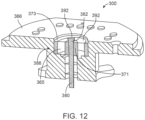
- a capacitor 365 is disposed within via 386 of the header 366.
- the capacitor 365 can include any suitable capacitor and can be electrically connected to the pin 380 and the header 366 using any suitable technique or techniques.
- an inner surface 371 of the capacitor 365 can be electrically connected to the pin 380, and an outer surface 373 of the capacitor can be electrically connected to the header 366.
- FIG. 16 is a schematic cross-section view of another embodiment of a feedthrough header assembly 600. All of the design considerations and possibilities described herein regarding feedthrough header assemblies 12, 100, 200, and 300 apply equally to feedthrough header assembly 600.
- feedthrough pin 680 and contact 690 are integral.
- An insulating layer or disk 691 can be disposed between the contact 690 and a recessed surface 669 of header 666 to electrically isolate the contact 690 from the header.
- disk 691 can be a ceramic disk.
- an insulative material 694 such as glass can be disposed between one or more portions of the feedthrough pin 680 and via 686 to electrically isolate the feedthrough pin from the header 666.
- insulative material 694 can instead be disposed between the recessed sidewalls of the recessed surface 669 and the contact 690.
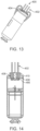
- FIGS. 13-14 are various views of another embodiment of a pacing device 400. All of the design considerations and possibilities described herein regarding implantable medical device 12 of FIGS. 1-8 apply equally to the implantable medical device 400 of FIGS. 13-14 .
- device 400 includes four feedthrough pins 402 that extend from an endcap 404 of the device.
- Each of the feedthrough pins 402 can be electrically connected to an electronic layer or layers of an electronics module (e.g., one or more electronic layers 40 of electronics module 32 of FIG. 7 ).
- each of the feedthrough pins 402 can have a solder joint 408 that connects the pin to an electronic layer.
- each of the feedthrough pins 402 can be disposed within a via 406 that extends through header 410.
- two or more of the feedthrough pins 402 can be disposed in the same via 406 and electrically isolated using an insulating material.
- each feedthrough pin 402 can be disposed in its own respective via 406. Further, each of the feedthrough pins 402 can extend beyond an outer surface of the header 410 as shown in FIG. 8 regarding feedthrough pin 80 and header 66.
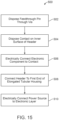
- FIG. 15 is a flowchart of one embodiment of a method 500 for forming the pacing device 12. Although described regarding pacing device 12 of FIGS. 1-8 , the method can be utilized to form any suitable implantable medical device.
- the feedthrough pin 80 can be disposed through the via 86 of the conductive header 66 using any suitable technique or techniques.
- a portion of the feedthrough pin 80 adjacent to the inner surface 68 of the conductive header 66 can be removed such that an end surface at the first end 82 of the feedthrough pin is in a plane defined by the inner surface 68 of the conductive header.
- Any suitable technique or techniques can be utilized to remove the portion of the feedthrough pin 80, e.g., the first end 82 can be planarized.
- the inner surface 68 can also be planarized along with the first end 82 of the feedthrough pin 80.
- one or more contacts 72 can be disposed on the inner surface 68 of the header 66 such that it is electrically connected to the header. Any suitable technique or techniques can be utilized to dispose the one or more contacts 72 on the inner surface 68.
- a seed layer e.g., seed layer 174 of FIG. 9
- a conductive layer e.g., conductive layer 176 of FIG. 9
- the seed layer and conductive layer can be patterned using any suitable technique or techniques
- a solder ball or contact pad e.g., solder ball 178 of FIG. 9
- the seed layer can be patterned prior to deposition of the conductive layer.
- the seed layer and conductive layer can be patterned together.
- one or more electronic components 64 of one or more electronic layers 40 can be electrically connected to the contact 72 such that the electronic component is electrically connected to the header 66.
- the major surface 56 of the substrate 54 of the electronic layer 48 i.e., the second major surface
- the feedthrough pin 80 can also be electrically connected to one or more electronic layers 40 using any suitable technique or techniques.
- the header 66 can be connected to the first end 6 of the elongated tubular housing 14 such that the electronics module 32 (e.g., one or more electronic layers 40) is disposed within the housing. Any suitable technique or techniques can be utilized to connect the header 66 to the first end 6 of the housing 14. In one or more embodiments, the endcap 26 is connected to the header 66, where the end cap defines the first end 6 of the housing 14.
- a power source e.g., battery 30
- a power source can be electrically connected to one or more of the electronic layers 40, e.g., by pressing a first side of the electronics module 32 against the electrical contact assembly 34.
- the first portion 22 of the housing 14 can be disposed over the electronics module 32 and connected to the second portion 24 of the housing 14 using any suitable technique or techniques, e.g., laser bonding.
- the end cap 26 can be connected to the header 66 of the feedthrough assembly 42 of the electronics module 32 using any suitable technique or techniques, e.g., welding.
- the described techniques may be implemented in hardware, software, firmware, or any combination thereof. If implemented in software, the functions may be stored as one or more instructions or code on a computer-readable medium and executed by a hardware-based processing unit.
- Computer-readable media may include computer-readable storage media, which corresponds to a tangible medium such as data storage media (e.g., RAM, ROM, EEPROM, flash memory, or any other medium that can be used to store desired program code in the form of instructions or data structures and that can be accessed by a computer).
- processors such as one or more digital signal processors (DSPs), general purpose microprocessors, application specific integrated circuits (ASICs), field programmable logic arrays (FPGAs), or other equivalent integrated or discrete logic circuitry.
- DSPs digital signal processors
- ASICs application specific integrated circuits
- FPGAs field programmable logic arrays
- processors may refer to any of the foregoing structure or any other physical structure suitable for implementation of the described techniques. Also, the techniques could be fully implemented in one or more circuits or logic elements.
Landscapes
- Health & Medical Sciences (AREA)
- Engineering & Computer Science (AREA)
- Life Sciences & Earth Sciences (AREA)
- Animal Behavior & Ethology (AREA)
- Radiology & Medical Imaging (AREA)
- Nuclear Medicine, Radiotherapy & Molecular Imaging (AREA)
- Biomedical Technology (AREA)
- General Health & Medical Sciences (AREA)
- Public Health (AREA)
- Veterinary Medicine (AREA)
- Manufacturing & Machinery (AREA)
- Electrotherapy Devices (AREA)
- Biophysics (AREA)
- Heart & Thoracic Surgery (AREA)
Claims (15)
- Elektronikmodul, umfassend:
eine Durchführungskopfanordnung (42), umfassend:einen leitenden Kopf (66) mit einer leitenden Innenfläche (68), einer Außenfläche (70) und einem auf der Innenfläche angeordneten und mit dem Kopf elektrisch verbundenen Kontakt; undeinen Durchführungsstift (80), der in einem Durchgang (86) angeordnet ist, der sich durch den Kopf zwischen der Innenfläche und der Außenfläche des Kopfes erstreckt, wobei der Durchführungsstift vom Kopf elektrisch isoliert ist und ein erstes Ende (82) angrenzend an die Innenfläche des Kopfes und ein zweites Ende (84) angrenzend an die Außenfläche des Kopfes aufweist; undeine elektronische Schicht (40), die ein Substrat und eine elektronische Komponente (64) umfasst, die auf oder in dem Substrat angeordnet ist, wobei die elektronische Komponente elektrisch mit dem Kontakt des leitenden Kopfes verbunden ist, so dass die elektronische Komponente elektrisch mit dem Kopf verbunden ist, und wobei ferner eine Hauptfläche des Substrats der elektronischen Schicht der leitenden Innenfläche des Kopfes zugewandt ist, ohne dass irgendwelche dazwischenliegenden nicht leitenden Schichten zwischen der Hauptfläche des Substrats und der leitenden Innenfläche des Kopfes angeordnet sind. - Modul nach Anspruch 1, ferner ein leitfähiges Kissen (290) umfassend, das am ersten Ende des Durchführungsstiftes angeordnet und mit dem Durchführungsstift elektrisch verbunden ist.
- Modul nach Anspruch 2, wobei das leitende Kissen in einer in der Innenfläche des leitenden Kopfes angeordneten vertieften Fläche (269) angeordnet ist, wobei das leitende Kissen vom Kopf durch eine nicht leitende Schicht, die zwischen dem leitenden Kissen und der vertieften Fläche angeordnet ist, elektrisch isoliert ist.
- Modul nach Anspruch 3, wobei die nicht leitende Schicht eine Keramikscheibe umfasst.
- Modul nach einem der Ansprüche 3 und 4, wobei die nicht leitende Schicht zwischen dem leitenden Kissen und einem oder mehreren Seitenabschnitten (267) der vertieften Fläche angeordnet ist.
- Modul nach einem der vorstehenden Ansprüche, ferner eine elektronische Kopfvorrichtung (392) umfassend, die am ersten Ende des Durchführungsstiftes angeordnet und mit dem Durchführungsstift elektrisch verbunden ist.
- Modul nach einem der vorstehenden Ansprüche, ferner einen zweiten Durchführungsstift umfassend, der in einem zweiten Durchgang angeordnet ist, der sich durch den Kopf zwischen der Innenfläche und der Außenfläche des Kopfes erstreckt, wobei der zweite Durchführungsstift vom Kopf elektrisch isoliert ist und ein erstes Ende angrenzend an die Innenfläche des Kopfes und ein zweites Ende angrenzend an die Außenfläche des Kopfes aufweist.
- Modul nach einem der vorstehenden Ansprüche, ferner einen Kondensator (365) umfassend, der innerhalb des Durchgangs des Kopfes angeordnet ist, wobei der Kondensator elektrisch mit dem Durchführungsstift und dem Kopf verbunden ist.
- Modul nach einem der vorstehenden Ansprüche, ferner ein Isoliermaterial (94) umfassend, das innerhalb des Durchgangs zwischen einem Wandteil (96) des Durchgangs und dem Durchführungsstift angeordnet ist.
- Implantierbare medizinische Vorrichtung, umfassend:eine Energiequelle (30); undein Elektronikmodul (32) nach Anspruch 1, das elektrisch mit der Energiequelle verbunden ist.
- Vorrichtung nach Anspruch 10, ferner ein längliches rohrförmiges Gehäuse (14) umfassend, das sich zwischen einem ersten Ende (6) und einem zweiten Ende (8) entlang einer Längsachse (10) erstreckt, und wobei ferner ein erster Abschnitt (22) des Gehäuses, der an das erste Ende angrenzt, das Elektronikmodul umschließt und ein zweiter Abschnitt (24) des Gehäuses, der an das zweite Ende angrenzt, die Energiequelle umschließt.
- Vorrichtung nach Anspruch 11, wobei der erste Abschnitt des länglichen rohrförmigen Gehäuses (14) ein im Wesentlichen transparentes Material umfasst.
- Vorrichtung nach Anspruch 11, wobei die Längsachse im Wesentlichen orthogonal zum Substrat der elektronischen Schicht (40) des Elektronikmoduls (32) verläuft.
- Vorrichtung nach einem der Ansprüche 10-13, ferner einen Kondensator (365) umfassend, der im Durchgang des Kopfes angeordnet ist, wobei der Kondensator elektrisch mit dem Durchführungsstift und dem Kopf verbunden ist; oder ferner isolierendes Material (94) umfassend, das im Durchgang (96) zwischen einem Wandabschnitt des Durchgangs und dem Durchführungsstift angeordnet ist.
- Vorrichtung nach einem der Ansprüche 10-14, wobei die elektronische Schicht (40) des Elektronikmoduls (32) so angeordnet ist, dass sie im Wesentlichen orthogonal zu einer Längsachse (10) der implantierbaren medizinischen Vorrichtung ist, insbesondere wobei die Hauptfläche des Substrats der elektronischen Schicht im Wesentlichen orthogonal zur Längsachse ist.
Applications Claiming Priority (3)
| Application Number | Priority Date | Filing Date | Title |
|---|---|---|---|
| US202163143996P | 2021-02-01 | 2021-02-01 | |
| US17/587,676 US12290693B2 (en) | 2021-02-01 | 2022-01-28 | Feedthrough header assembly and device including same |
| PCT/US2022/014484 WO2022165297A1 (en) | 2021-02-01 | 2022-01-31 | Feedthrough header assembly and device including same |
Publications (2)
| Publication Number | Publication Date |
|---|---|
| EP4284495A1 EP4284495A1 (de) | 2023-12-06 |
| EP4284495B1 true EP4284495B1 (de) | 2025-06-25 |
Family
ID=82612009
Family Applications (1)
| Application Number | Title | Priority Date | Filing Date |
|---|---|---|---|
| EP22704698.4A Active EP4284495B1 (de) | 2021-02-01 | 2022-01-31 | Durchführungskopfanordnung und vorrichtung damit |
Country Status (3)
| Country | Link |
|---|---|
| US (1) | US12290693B2 (de) |
| EP (1) | EP4284495B1 (de) |
| CN (1) | CN116801943A (de) |
Families Citing this family (2)
| Publication number | Priority date | Publication date | Assignee | Title |
|---|---|---|---|---|
| CN116056756A (zh) * | 2020-09-09 | 2023-05-02 | 美敦力公司 | 电子封装和包括该电子封装的植入式医疗装置 |
| WO2025158310A1 (en) | 2024-01-24 | 2025-07-31 | Medtronic, Inc. | Pressure sensor assembly and implantable medical device including same |
Citations (3)
| Publication number | Priority date | Publication date | Assignee | Title |
|---|---|---|---|---|
| US10029107B1 (en) * | 2017-01-26 | 2018-07-24 | Cardiac Pacemakers, Inc. | Leadless device with overmolded components |
| WO2021086877A1 (en) * | 2019-10-29 | 2021-05-06 | Medtronic, Inc. | Electronics assembly for implantable medical device |
| WO2021127311A1 (en) * | 2019-12-19 | 2021-06-24 | Medtronic, Inc. | Feedthrough assembly and device including same |
Family Cites Families (19)
| Publication number | Priority date | Publication date | Assignee | Title |
|---|---|---|---|---|
| US5595514A (en) * | 1994-07-19 | 1997-01-21 | Santa Barbara Research Center | Feedthrough pin and process for its preparation, and electrical feedthrough made therewith |
| CA2482202C (en) * | 2001-04-13 | 2012-07-03 | Surgi-Vision, Inc. | Systems and methods for magnetic-resonance-guided interventional procedures |
| US7211884B1 (en) * | 2002-01-28 | 2007-05-01 | Pacesetter, Inc. | Implantable medical device construction using a flexible substrate |
| US7061949B1 (en) * | 2002-08-16 | 2006-06-13 | Jds Uniphase Corporation | Methods, apparatus, and systems with semiconductor laser packaging for high modulation bandwidth |
| US6999818B2 (en) | 2003-05-23 | 2006-02-14 | Greatbatch-Sierra, Inc. | Inductor capacitor EMI filter for human implant applications |
| US20120256704A1 (en) | 2011-03-01 | 2012-10-11 | Greatbatch Ltd. | Rf filter for an active medical device (amd) for handling high rf power induced in an associated implanted lead from an external rf field |
| CN101877448B (zh) * | 2009-04-29 | 2012-11-28 | 富士康(昆山)电脑接插件有限公司 | 模组连接器 |
| US8725263B2 (en) * | 2009-07-31 | 2014-05-13 | Medtronic, Inc. | Co-fired electrical feedthroughs for implantable medical devices having a shielded RF conductive path and impedance matching |
| US8433409B2 (en) | 2010-01-29 | 2013-04-30 | Medtronic, Inc. | Implantable medical device battery |
| US8659870B2 (en) | 2010-11-22 | 2014-02-25 | Greatbatch Ltd. | Modular EMI filtered terminal assembly for an active implantable medical device |
| EP3366348B1 (de) | 2012-01-16 | 2023-08-23 | Greatbatch Ltd. | Emi-gefilterte co-verbundene hermetische durchführung, durchführungskondensator und leitungsanordnung für eine aktive implantierbare medizinische vorrichtung |
| US8954151B2 (en) * | 2013-01-29 | 2015-02-10 | Boston Scientific Neuromodulation Corporation | RF resistant feedthrough assembly and electrical stimulation systems containing the assembly |
| US10124559B2 (en) | 2014-12-24 | 2018-11-13 | Medtronic, Inc. | Kinetically limited nano-scale diffusion bond structures and methods |
| BR102015016848A2 (pt) * | 2015-03-16 | 2015-12-15 | Medtronic Inc | dispositivo médico implantável |
| US10098589B2 (en) * | 2015-12-21 | 2018-10-16 | Medtronic, Inc. | Sealed package and method of forming same |
| US10583300B2 (en) | 2017-07-27 | 2020-03-10 | Pacesetter, Inc. | Leadless implantable medical device with fixation antenna member |
| US20200111765A1 (en) * | 2018-10-09 | 2020-04-09 | Medtronic, Inc. | Electronic assembly and method of forming same |
| US11247059B2 (en) * | 2018-11-20 | 2022-02-15 | Pacesetter, Inc. | Biostimulator having flexible circuit assembly |
| US20240055159A1 (en) * | 2021-01-12 | 2024-02-15 | Micro Motion, Inc. | Electrical junction having an improved feedthrough element |
-
2022
- 2022-01-28 US US17/587,676 patent/US12290693B2/en active Active
- 2022-01-31 CN CN202280012654.9A patent/CN116801943A/zh active Pending
- 2022-01-31 EP EP22704698.4A patent/EP4284495B1/de active Active
Patent Citations (3)
| Publication number | Priority date | Publication date | Assignee | Title |
|---|---|---|---|---|
| US10029107B1 (en) * | 2017-01-26 | 2018-07-24 | Cardiac Pacemakers, Inc. | Leadless device with overmolded components |
| WO2021086877A1 (en) * | 2019-10-29 | 2021-05-06 | Medtronic, Inc. | Electronics assembly for implantable medical device |
| WO2021127311A1 (en) * | 2019-12-19 | 2021-06-24 | Medtronic, Inc. | Feedthrough assembly and device including same |
Also Published As
| Publication number | Publication date |
|---|---|
| CN116801943A (zh) | 2023-09-22 |
| EP4284495A1 (de) | 2023-12-06 |
| US20220241598A1 (en) | 2022-08-04 |
| US12290693B2 (en) | 2025-05-06 |
Similar Documents
| Publication | Publication Date | Title |
|---|---|---|
| US12220590B2 (en) | Feedthrough assembly and device including same | |
| US11103714B2 (en) | Sealed implantable medical device and method of forming same | |
| EP2988821B1 (de) | Elektrodenanordnungen und zugehörige fixierelemente für implantierbare medizinische vorrichtungen | |
| CN110234392B (zh) | 具有被包覆模制的组件的无引线装置 | |
| US11647600B2 (en) | Sealed package and method of forming same | |
| EP3870267B1 (de) | Biostimulatordurchführung mit integriertem elektrodennapf | |
| US20240165416A1 (en) | Electronics assembly for implantable medical device | |
| US12290693B2 (en) | Feedthrough header assembly and device including same | |
| US12290690B2 (en) | Biostimulator having patch antenna | |
| EP4475940B1 (de) | Durchführungsanordnung und implantierbare medizinische vorrichtung damit | |
| WO2022165297A1 (en) | Feedthrough header assembly and device including same | |
| EP4284498B1 (de) | Elektronisches gehäuse und vorrichtung damit | |
| WO2023152610A1 (en) | Feedthrough assembly and implantable medical device including same | |
| US12082354B2 (en) | Electronic package and device including same | |
| US20240244781A1 (en) | Header laser etching feedthrough for ceramic bonding |
Legal Events
| Date | Code | Title | Description |
|---|---|---|---|
| STAA | Information on the status of an ep patent application or granted ep patent |
Free format text: STATUS: UNKNOWN |
|
| STAA | Information on the status of an ep patent application or granted ep patent |
Free format text: STATUS: THE INTERNATIONAL PUBLICATION HAS BEEN MADE |
|
| PUAI | Public reference made under article 153(3) epc to a published international application that has entered the european phase |
Free format text: ORIGINAL CODE: 0009012 |
|
| STAA | Information on the status of an ep patent application or granted ep patent |
Free format text: STATUS: REQUEST FOR EXAMINATION WAS MADE |
|
| 17P | Request for examination filed |
Effective date: 20230829 |
|
| AK | Designated contracting states |
Kind code of ref document: A1 Designated state(s): AL AT BE BG CH CY CZ DE DK EE ES FI FR GB GR HR HU IE IS IT LI LT LU LV MC MK MT NL NO PL PT RO RS SE SI SK SM TR |
|
| DAV | Request for validation of the european patent (deleted) | ||
| DAX | Request for extension of the european patent (deleted) | ||
| GRAP | Despatch of communication of intention to grant a patent |
Free format text: ORIGINAL CODE: EPIDOSNIGR1 |
|
| STAA | Information on the status of an ep patent application or granted ep patent |
Free format text: STATUS: GRANT OF PATENT IS INTENDED |
|
| INTG | Intention to grant announced |
Effective date: 20240910 |
|
| GRAJ | Information related to disapproval of communication of intention to grant by the applicant or resumption of examination proceedings by the epo deleted |
Free format text: ORIGINAL CODE: EPIDOSDIGR1 |
|
| STAA | Information on the status of an ep patent application or granted ep patent |
Free format text: STATUS: REQUEST FOR EXAMINATION WAS MADE |
|
| GRAP | Despatch of communication of intention to grant a patent |
Free format text: ORIGINAL CODE: EPIDOSNIGR1 |
|
| STAA | Information on the status of an ep patent application or granted ep patent |
Free format text: STATUS: GRANT OF PATENT IS INTENDED |
|
| INTC | Intention to grant announced (deleted) | ||
| INTG | Intention to grant announced |
Effective date: 20250117 |
|
| GRAS | Grant fee paid |
Free format text: ORIGINAL CODE: EPIDOSNIGR3 |
|
| GRAA | (expected) grant |
Free format text: ORIGINAL CODE: 0009210 |
|
| STAA | Information on the status of an ep patent application or granted ep patent |
Free format text: STATUS: THE PATENT HAS BEEN GRANTED |
|
| AK | Designated contracting states |
Kind code of ref document: B1 Designated state(s): AL AT BE BG CH CY CZ DE DK EE ES FI FR GB GR HR HU IE IS IT LI LT LU LV MC MK MT NL NO PL PT RO RS SE SI SK SM TR |
|
| REG | Reference to a national code |
Ref country code: GB Ref legal event code: FG4D |
|
| REG | Reference to a national code |
Ref country code: CH Ref legal event code: EP |
|
| REG | Reference to a national code |
Ref country code: DE Ref legal event code: R096 Ref document number: 602022016417 Country of ref document: DE |
|
| REG | Reference to a national code |
Ref country code: CH Ref legal event code: EP |
|
| REG | Reference to a national code |
Ref country code: IE Ref legal event code: FG4D |
|
| PG25 | Lapsed in a contracting state [announced via postgrant information from national office to epo] |
Ref country code: FI Free format text: LAPSE BECAUSE OF FAILURE TO SUBMIT A TRANSLATION OF THE DESCRIPTION OR TO PAY THE FEE WITHIN THE PRESCRIBED TIME-LIMIT Effective date: 20250625 |
|
| REG | Reference to a national code |
Ref country code: LT Ref legal event code: MG9D |
|
| PG25 | Lapsed in a contracting state [announced via postgrant information from national office to epo] |
Ref country code: NO Free format text: LAPSE BECAUSE OF FAILURE TO SUBMIT A TRANSLATION OF THE DESCRIPTION OR TO PAY THE FEE WITHIN THE PRESCRIBED TIME-LIMIT Effective date: 20250925 Ref country code: GR Free format text: LAPSE BECAUSE OF FAILURE TO SUBMIT A TRANSLATION OF THE DESCRIPTION OR TO PAY THE FEE WITHIN THE PRESCRIBED TIME-LIMIT Effective date: 20250926 |
|
| PG25 | Lapsed in a contracting state [announced via postgrant information from national office to epo] |
Ref country code: BG Free format text: LAPSE BECAUSE OF FAILURE TO SUBMIT A TRANSLATION OF THE DESCRIPTION OR TO PAY THE FEE WITHIN THE PRESCRIBED TIME-LIMIT Effective date: 20250625 |
|
| PG25 | Lapsed in a contracting state [announced via postgrant information from national office to epo] |
Ref country code: HR Free format text: LAPSE BECAUSE OF FAILURE TO SUBMIT A TRANSLATION OF THE DESCRIPTION OR TO PAY THE FEE WITHIN THE PRESCRIBED TIME-LIMIT Effective date: 20250625 |
|
| PG25 | Lapsed in a contracting state [announced via postgrant information from national office to epo] |
Ref country code: RS Free format text: LAPSE BECAUSE OF FAILURE TO SUBMIT A TRANSLATION OF THE DESCRIPTION OR TO PAY THE FEE WITHIN THE PRESCRIBED TIME-LIMIT Effective date: 20250925 |
|
| PG25 | Lapsed in a contracting state [announced via postgrant information from national office to epo] |
Ref country code: LV Free format text: LAPSE BECAUSE OF FAILURE TO SUBMIT A TRANSLATION OF THE DESCRIPTION OR TO PAY THE FEE WITHIN THE PRESCRIBED TIME-LIMIT Effective date: 20250625 |
|
| REG | Reference to a national code |
Ref country code: NL Ref legal event code: MP Effective date: 20250625 |
|
| PG25 | Lapsed in a contracting state [announced via postgrant information from national office to epo] |
Ref country code: NL Free format text: LAPSE BECAUSE OF FAILURE TO SUBMIT A TRANSLATION OF THE DESCRIPTION OR TO PAY THE FEE WITHIN THE PRESCRIBED TIME-LIMIT Effective date: 20250625 |
|
| PG25 | Lapsed in a contracting state [announced via postgrant information from national office to epo] |
Ref country code: PT Free format text: LAPSE BECAUSE OF FAILURE TO SUBMIT A TRANSLATION OF THE DESCRIPTION OR TO PAY THE FEE WITHIN THE PRESCRIBED TIME-LIMIT Effective date: 20251027 |
|
| REG | Reference to a national code |
Ref country code: AT Ref legal event code: MK05 Ref document number: 1805870 Country of ref document: AT Kind code of ref document: T Effective date: 20250625 |
|
| PG25 | Lapsed in a contracting state [announced via postgrant information from national office to epo] |
Ref country code: IS Free format text: LAPSE BECAUSE OF FAILURE TO SUBMIT A TRANSLATION OF THE DESCRIPTION OR TO PAY THE FEE WITHIN THE PRESCRIBED TIME-LIMIT Effective date: 20251025 |
|
| PG25 | Lapsed in a contracting state [announced via postgrant information from national office to epo] |
Ref country code: AT Free format text: LAPSE BECAUSE OF FAILURE TO SUBMIT A TRANSLATION OF THE DESCRIPTION OR TO PAY THE FEE WITHIN THE PRESCRIBED TIME-LIMIT Effective date: 20250625 Ref country code: SM Free format text: LAPSE BECAUSE OF FAILURE TO SUBMIT A TRANSLATION OF THE DESCRIPTION OR TO PAY THE FEE WITHIN THE PRESCRIBED TIME-LIMIT Effective date: 20250625 |
|
| PGFP | Annual fee paid to national office [announced via postgrant information from national office to epo] |
Ref country code: FR Payment date: 20251217 Year of fee payment: 5 |
|
| PG25 | Lapsed in a contracting state [announced via postgrant information from national office to epo] |
Ref country code: CZ Free format text: LAPSE BECAUSE OF FAILURE TO SUBMIT A TRANSLATION OF THE DESCRIPTION OR TO PAY THE FEE WITHIN THE PRESCRIBED TIME-LIMIT Effective date: 20250625 |
|
| PGFP | Annual fee paid to national office [announced via postgrant information from national office to epo] |
Ref country code: IE Payment date: 20251218 Year of fee payment: 5 |
|
| PG25 | Lapsed in a contracting state [announced via postgrant information from national office to epo] |
Ref country code: PL Free format text: LAPSE BECAUSE OF FAILURE TO SUBMIT A TRANSLATION OF THE DESCRIPTION OR TO PAY THE FEE WITHIN THE PRESCRIBED TIME-LIMIT Effective date: 20250625 |
|
| PG25 | Lapsed in a contracting state [announced via postgrant information from national office to epo] |
Ref country code: EE Free format text: LAPSE BECAUSE OF FAILURE TO SUBMIT A TRANSLATION OF THE DESCRIPTION OR TO PAY THE FEE WITHIN THE PRESCRIBED TIME-LIMIT Effective date: 20250625 |
|
| PG25 | Lapsed in a contracting state [announced via postgrant information from national office to epo] |
Ref country code: SK Free format text: LAPSE BECAUSE OF FAILURE TO SUBMIT A TRANSLATION OF THE DESCRIPTION OR TO PAY THE FEE WITHIN THE PRESCRIBED TIME-LIMIT Effective date: 20250625 |
|
| PG25 | Lapsed in a contracting state [announced via postgrant information from national office to epo] |
Ref country code: ES Free format text: LAPSE BECAUSE OF FAILURE TO SUBMIT A TRANSLATION OF THE DESCRIPTION OR TO PAY THE FEE WITHIN THE PRESCRIBED TIME-LIMIT Effective date: 20250625 |
|
| REG | Reference to a national code |
Ref country code: DE Ref legal event code: R097 Ref document number: 602022016417 Country of ref document: DE |
|
| PG25 | Lapsed in a contracting state [announced via postgrant information from national office to epo] |
Ref country code: DK Free format text: LAPSE BECAUSE OF FAILURE TO SUBMIT A TRANSLATION OF THE DESCRIPTION OR TO PAY THE FEE WITHIN THE PRESCRIBED TIME-LIMIT Effective date: 20250625 |
|
| PGFP | Annual fee paid to national office [announced via postgrant information from national office to epo] |
Ref country code: DE Payment date: 20251217 Year of fee payment: 5 |
|
| PG25 | Lapsed in a contracting state [announced via postgrant information from national office to epo] |
Ref country code: IT Free format text: LAPSE BECAUSE OF FAILURE TO SUBMIT A TRANSLATION OF THE DESCRIPTION OR TO PAY THE FEE WITHIN THE PRESCRIBED TIME-LIMIT Effective date: 20250625 |
|
| PLBE | No opposition filed within time limit |
Free format text: ORIGINAL CODE: 0009261 |
|
| STAA | Information on the status of an ep patent application or granted ep patent |
Free format text: STATUS: NO OPPOSITION FILED WITHIN TIME LIMIT |
|
| REG | Reference to a national code |
Ref country code: CH Ref legal event code: L10 Free format text: ST27 STATUS EVENT CODE: U-0-0-L10-L00 (AS PROVIDED BY THE NATIONAL OFFICE) Effective date: 20260507 |