EP4284487B1 - Stromerzeugungarchitektur für eine implantierbare stimulatorvorrichtung - Google Patents
Stromerzeugungarchitektur für eine implantierbare stimulatorvorrichtung Download PDFInfo
- Publication number
- EP4284487B1 EP4284487B1 EP22714096.9A EP22714096A EP4284487B1 EP 4284487 B1 EP4284487 B1 EP 4284487B1 EP 22714096 A EP22714096 A EP 22714096A EP 4284487 B1 EP4284487 B1 EP 4284487B1
- Authority
- EP
- European Patent Office
- Prior art keywords
- current
- dac
- electrode
- offset
- iref
- Prior art date
- Legal status (The legal status is an assumption and is not a legal conclusion. Google has not performed a legal analysis and makes no representation as to the accuracy of the status listed.)
- Active
Links
Images


Classifications
-
- H—ELECTRICITY
- H03—ELECTRONIC CIRCUITRY
- H03M—CODING; DECODING; CODE CONVERSION IN GENERAL
- H03M1/00—Analogue/digital conversion; Digital/analogue conversion
- H03M1/10—Calibration or testing
- H03M1/1009—Calibration
- H03M1/1033—Calibration over the full range of the converter, e.g. for correcting differential non-linearity
- H03M1/1057—Calibration over the full range of the converter, e.g. for correcting differential non-linearity by trimming, i.e. by individually adjusting at least part of the quantisation value generators or stages to their nominal values
- H03M1/1061—Calibration over the full range of the converter, e.g. for correcting differential non-linearity by trimming, i.e. by individually adjusting at least part of the quantisation value generators or stages to their nominal values using digitally programmable trimming circuits
-
- A—HUMAN NECESSITIES
- A61—MEDICAL OR VETERINARY SCIENCE; HYGIENE
- A61N—ELECTROTHERAPY; MAGNETOTHERAPY; RADIATION THERAPY; ULTRASOUND THERAPY
- A61N1/00—Electrotherapy; Circuits therefor
- A61N1/02—Details
- A61N1/025—Digital circuitry features of electrotherapy devices, e.g. memory, clocks, processors
-
- A—HUMAN NECESSITIES
- A61—MEDICAL OR VETERINARY SCIENCE; HYGIENE
- A61N—ELECTROTHERAPY; MAGNETOTHERAPY; RADIATION THERAPY; ULTRASOUND THERAPY
- A61N1/00—Electrotherapy; Circuits therefor
- A61N1/02—Details
- A61N1/04—Electrodes
- A61N1/05—Electrodes for implantation or insertion into the body, e.g. heart electrode
- A61N1/0551—Spinal or peripheral nerve electrodes
-
- A—HUMAN NECESSITIES
- A61—MEDICAL OR VETERINARY SCIENCE; HYGIENE
- A61N—ELECTROTHERAPY; MAGNETOTHERAPY; RADIATION THERAPY; ULTRASOUND THERAPY
- A61N1/00—Electrotherapy; Circuits therefor
- A61N1/02—Details
- A61N1/08—Arrangements or circuits for monitoring, protecting, controlling or indicating
-
- A—HUMAN NECESSITIES
- A61—MEDICAL OR VETERINARY SCIENCE; HYGIENE
- A61N—ELECTROTHERAPY; MAGNETOTHERAPY; RADIATION THERAPY; ULTRASOUND THERAPY
- A61N1/00—Electrotherapy; Circuits therefor
- A61N1/14—Leading-off electric charges, e.g. by earthing
-
- A—HUMAN NECESSITIES
- A61—MEDICAL OR VETERINARY SCIENCE; HYGIENE
- A61N—ELECTROTHERAPY; MAGNETOTHERAPY; RADIATION THERAPY; ULTRASOUND THERAPY
- A61N1/00—Electrotherapy; Circuits therefor
- A61N1/18—Applying electric currents by contact electrodes
- A61N1/32—Applying electric currents by contact electrodes alternating or intermittent currents
- A61N1/36—Applying electric currents by contact electrodes alternating or intermittent currents for stimulation
- A61N1/3605—Implantable neurostimulators for stimulating central or peripheral nerve system
- A61N1/3606—Implantable neurostimulators for stimulating central or peripheral nerve system adapted for a particular treatment
- A61N1/36062—Spinal stimulation
-
- A—HUMAN NECESSITIES
- A61—MEDICAL OR VETERINARY SCIENCE; HYGIENE
- A61N—ELECTROTHERAPY; MAGNETOTHERAPY; RADIATION THERAPY; ULTRASOUND THERAPY
- A61N1/00—Electrotherapy; Circuits therefor
- A61N1/18—Applying electric currents by contact electrodes
- A61N1/32—Applying electric currents by contact electrodes alternating or intermittent currents
- A61N1/36—Applying electric currents by contact electrodes alternating or intermittent currents for stimulation
- A61N1/3605—Implantable neurostimulators for stimulating central or peripheral nerve system
- A61N1/36125—Details of circuitry or electric components
-
- A—HUMAN NECESSITIES
- A61—MEDICAL OR VETERINARY SCIENCE; HYGIENE
- A61N—ELECTROTHERAPY; MAGNETOTHERAPY; RADIATION THERAPY; ULTRASOUND THERAPY
- A61N1/00—Electrotherapy; Circuits therefor
- A61N1/18—Applying electric currents by contact electrodes
- A61N1/32—Applying electric currents by contact electrodes alternating or intermittent currents
- A61N1/36—Applying electric currents by contact electrodes alternating or intermittent currents for stimulation
- A61N1/3605—Implantable neurostimulators for stimulating central or peripheral nerve system
- A61N1/36128—Control systems
- A61N1/36142—Control systems for improving safety
-
- A—HUMAN NECESSITIES
- A61—MEDICAL OR VETERINARY SCIENCE; HYGIENE
- A61N—ELECTROTHERAPY; MAGNETOTHERAPY; RADIATION THERAPY; ULTRASOUND THERAPY
- A61N1/00—Electrotherapy; Circuits therefor
- A61N1/18—Applying electric currents by contact electrodes
- A61N1/32—Applying electric currents by contact electrodes alternating or intermittent currents
- A61N1/36—Applying electric currents by contact electrodes alternating or intermittent currents for stimulation
- A61N1/372—Arrangements in connection with the implantation of stimulators
- A61N1/378—Electrical supply
Definitions
- the present invention relates generally to medical devices, and more particularly to improved current generation architectures for an implantable pulse generator.
- Implantable stimulation devices are devices that generate and deliver electrical stimuli to body nerves and tissues for the therapy of various biological disorders, such as pacemakers to treat cardiac arrhythmia, defibrillators to treat cardiac fibrillation, cochlear stimulators to treat deafness, retinal stimulators to treat blindness, muscle stimulators to produce coordinated limb movement, spinal cord stimulators to treat chronic pain, cortical and deep brain stimulators to treat motor and psychological disorders, and other neural stimulators to treat urinary incontinence, sleep apnea, shoulder subluxation, etc.
- SCS Spinal Cord Stimulation
- the present invention may find applicability in any implantable medical device system, including a Deep Brain Stimulation (DBS) system.
- DBS Deep Brain Stimulation
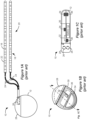
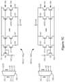
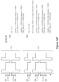
- an SCS system typically includes an Implantable Pulse Generator (IPG) 10, which includes a biocompatible device case 12 formed of a conductive material such as titanium for example.
- the case 12 typically holds the circuitry and power source (e.g., battery) 14 ( Fig. 1C ) necessary for the IPG 10 to function, although IPGs can also be powered via external RF energy and without a battery.
- the IPG 10 is coupled to electrodes 16 via one or more electrode leads 18, such that the electrodes 16 form an electrode array 20.
- the electrodes 16 are carried on a flexible body 22, which also houses the individual signal wires 24 coupled to each electrode.
- Electrodes there are eight electrodes (Ei) on two leads 18 for a total of sixteen electrodes 16, although the number of leads and electrodes is application specific and therefore can vary.
- the leads 18 couple to the IPG 10 using lead connectors 26, which are fixed in a non-conductive header material 28, which can comprise an epoxy for example.
- the IPG 10 typically includes a printed circuit board (PCB) 30, along with various electronic components 32 mounted to the PCB 30, some of which are discussed subsequently.
- PCB printed circuit board
- Two coils are shown in the IPG 10: a telemetry coil 34 used to transmit/receive data to/from an external controller such as a clinician programmer or a hand-held patient programmer used to program stimulation in the IPG (not shown); and a charging coil 36 for charging or recharging the IPG's battery 14 using an external charger (not shown).
- Figure 1B shows these aspects in perspective with the case 12 removed for easier viewing.
- Telemetry coil 34 may alternatively comprise a short range RF antenna for wirelessly communicating in accordance with a short-range RF standard such as Bluetooth, WiFi, MICS, Zigbee, etc., as described in U.S. Patent Application Publication 2016/0051825 .
- a short-range RF standard such as Bluetooth, WiFi, MICS, Zigbee, etc.
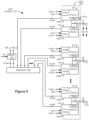
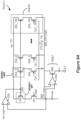
- Microcontroller 50 and ASIC 60 comprise monolithic integrated circuits each formed on their own semiconductive substrates ("chips"), and each may be contained in its own package and mounted to the IPG 10's PCB 30.
- Architecture 40 may also include additional memory (not shown) for storage of programs or data beyond that provided internally in the microcontroller 50. Additional memory may be connected to the microcontroller 50 by a serial interface (SI) as shown, but could also communicate with the microcontroller 50 via bus 90.
- Bus 90 may comprise a parallel address/data bus, and may include a clock signal and various control signals to dictate reading and writing to various memory locations, as explained in the above-referenced '529 Publication. Bus 90 and the signals it carries may also take different forms; for example, bus 90 may include separate address and data lines, may be serial in nature, etc.
- FIG. 2B shows various functional circuit blocks within ASIC 60, which are briefly described.
- ASIC 60 includes an internal bus 92 which can couple to external bus 90 and which may duplicate bus 90's signals.
- each of the functional blocks includes interface circuitry 88 enabling communication on the internal bus 92 and ultimately external bus 90, as the above-referenced ASIC Publications explain.
- Interface circuitry 88 includes circuitry to help each block recognize when bus 92 is communicating data with addresses belonging to that block.
- ASIC 60 contains several terminals 61 (e.g., pins, bond pads, solder bumps, etc.), such as those necessary to connect to the bus 90, the battery 14, the coils 34, 36, external memory (not shown).
- Terminals 61 include electrode node terminals 61a (E1'-E16') which connect to the electrodes 16 (E1-E16) on the lead(s) 18 by way of DC-blocking capacitors 55.
- DC-blocking capacitors 55 are useful to ensure that DC current isn't inadvertently (e.g., in the event of failure of the ASIC 60's circuitry) injected into the patient's tissue, and hence provide safety to the IPG 10.
- Such DC-blocking capacitors 55 can be located on or in the IPG 10's PCB 30 ( Fig. 1C ) inside of the IPG's case 12. See U.S. Patent Application Publication 2015/0157861 .
- Analog-to-Digital (A/D) block 66 digitizes various analog signals for interpretation by the IPG 10, such as the battery voltage Vbat or voltages appearing at the electrodes, and is coupled to an analog bus 67 containing such voltages.
- A/D block 66 may further receive signals from sample and hold block 68, which as the ASIC Publications explain can be used to measure such voltages, or differences between two voltages.
- sample and hold circuitry 68 may receive voltages from two electrodes and provide a difference between them (see, e.g., VE1-VE2 in Fig. 3 , discussed subsequently), which difference voltage may then be digitized at A/D block 66. Knowing the difference in voltage between two electrodes when they pass a constant current allows for a determination of the (tissue) resistance between them, which is useful for a variety of reasons.
- Sample and hold block 68 may also be used to determine one or more voltage drops across the DAC circuitry 72 (see Vp and Vn in Fig. 3 , explained subsequently) used to create the stimulation pulses. This is useful to setting the compliance voltage VH output by a compliance voltage generator block 76. Compliance voltage VH powers the DAC circuitry 72, and the measured voltage drops can be used to ensure that the compliance voltage VH produced is optimal for the stimulation current to be provided-i.e., VH is not too low to be unable to produce the current required for the stimulation, nor too high so as to waste power in the IPG 10.
- Compliance voltage generator block 76 includes circuitry for boosting a power supply voltage such as the battery voltage, Vbat, to a proper level for VH.
- Such circuitry can include an inductor-based boost converter or a capacitor-based charge pump, which are described in detail in U.S. Patent Application Publication 2010/0211132 .
- Clock generation block 74 can be used to generate a clock for the ASIC 60 and for communication on the bus 92.
- Clock generation block 74 may receive an oscillating signal from an off-chip crystal oscillator 56, or may comprise other forms of clock circuitry located completely on chip, such as a ring oscillator.
- U.S. Patent Application Publication 2014/0266375 discloses another on-chip circuit that can be used to generate a clock signal on the ASIC 60.
- Master/slave control block 86 can be used to inform the ASIC 60 whether it is to be used as a master ASIC or as a slave ASIC (e.g., 60'), which may be bond programmed at M/S terminal 61.
- M/S terminal may be connected to a power supply voltage (e.g., Vbat) to inform ASIC 60 that it will operate as a master ASIC, or to ground to inform that it will operate as a slave, in which case certain function blacks will be disabled, as the ASIC Publications explain.
- Vbat power supply voltage
- Interrupt controller block 80 receives various interrupts (e.g., INT1-INT4) from other circuit blocks, which because of their immediate importance are received independent of the bus 92 and its communication protocol. Interrupts may also be sent to the microcontroller 50 via the bus 90. Internal controller 82 in the ASIC 60 may receive indication of such interrupts, and act a controller for all other circuit blocks, to the extent microcontroller 50 ( Fig. 2A ) does not handle such interrupts through the external bus 90. Further, each of the functional circuit blocks contain set-up and status registers (not shown) written to by the controller 82 upon initialization to configure and enable each block.
- interrupts e.g., INT1-INT4
- Internal controller 82 in the ASIC 60 may receive indication of such interrupts, and act a controller for all other circuit blocks, to the extent microcontroller 50 ( Fig. 2A ) does not handle such interrupts through the external bus 90.
- each of the functional circuit blocks contain set-up and status registers (not shown) written to by the controller
- Each functional block can then write pertinent data at its status registers, which can in turn be read by the controller 82 via internal bus 92 as necessary, or by the microcontroller 50 via external bus 90.
- the functional circuit blocks can further include simple state machines to manage their operation, which state machines are enabled and modified via each block's set-up and status registers.
- Nonvolatile memory (NOVO) block 78 caches any relevant data in the system (such as log data). Additional memory (not shown) can also be provided off-chip via a serial interface block 84.
- ASIC 60 further includes a stimulation circuit block 70, which includes circuitry for receiving and storing stimulation parameters from the microcontroller 50 via buses 90 and 92.
- Stimulation parameters define the shape and timing of stimulation pulses to be formed at the electrodes, and can include parameters such as which electrodes E1-E16 will be active; whether those active electrodes are to act as anodes that source current to a patient's tissue, or cathodes that sink current from the tissue; and the amplitude (A), duration (D), and frequency (f) of the pulses. Amplitude may comprise a voltage or current amplitude.
- Such stimulation parameters may be stored in registers in the stimulation circuitry block 70. See, e.g., U.S. Patent Application Publications 2013/0289661 ; 2013/0184794 .
- Block 70 also includes a Digital-to-Analog Converter circuitry (DAC) 72 for receiving the stimulation parameters from the registers and for forming the prescribed pulses at the selected electrodes.
- DAC Digital-to-Analog Converter circuitry
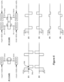
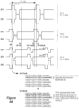
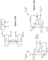
- Figure 3 shows a simple example of DAC circuitry 72 as used to provide a current pulse between selected electrodes E1 and E2 and through a patient's tissue, Rt.
- DAC circuitry 72 as shown comprises two portions, denoted as PDAC 72p and NDAC 72n. These portions of DAC circuitry 72 are so named because of the polarity of the transistors used to build them and the polarity of the current they provide.
- PDAC 72p is formed from P-channel transistors and is used to source a current +I to the patient's tissue Rt via a selected electrode E1 operating as an anode.
- NDAC 72n is formed of N-channel transistors and is used to sink current -I from the patient's tissue via a selected electrode E2. It is important that current sourced to the tissue at any given time equal that sunk from the tissue to prevent charge from building in the tissue, although more than one anode electrode and more than one cathode electrode may be operable at a given time.
- PDAC 72p and NDAC 72n receive digital control signals from the registers in the stimulation circuitry block 70, denoted ⁇ Pstim> and ⁇ Nstim> respectively, to generate the prescribed pulses with the prescribed timing.
- PDAC 72p and NDAC 72n comprise current sources, and in particular include current-mirrored transistors for mirroring a reference current Iref to produce pulses with an amplitude (A) of I.
- PDAC 72p and NDAC 72n could however also comprise constant voltage sources.
- Control signals ⁇ Pstim> and ⁇ Nstim> also prescribe the timing of the pulses, including their duration (D) and frequency (f), as shown in the waveforms generated at the selected electrodes.
- the PDAC 72p and NDAC 72n along with the intervening tissue Rt complete a circuit between a power supply VH-the compliance voltage as already introduced-and ground.
- the compliance voltage VH is adjustable to an optimal level at compliance voltage generator block 76 ( Fig. 2B ) to ensure that current pulses of a prescribed amplitude can be produced without unnecessarily wasting IPG power.
- the DAC circuitry 72 may be dedicated at each of the electrodes, and thus may be activated only when its associated electrode is selected as an anode or cathode. See, e.g., USP 6,181,969 .
- one or more DACs may be distributed to a selected electrode by a switch matrix (not shown), in which case optional control signals ⁇ Psel> and ⁇ Nsel> would be used to control the switch matrix and establish the connection between the selected electrode and the PDAC 72p or NDAC 72n.
- DAC circuitry 72 may also use a combination of these dedicated and distributed approaches. See, e.g., USP 8,620,436 .
- the pulses provided at the electrodes are biphasic, meaning that each pulse comprises a first phase 94a of a first polarity, followed by a second phase 94b of an opposite polarity.
- This is useful as a means of active recovery of charge that may build up on the DC-blocking capacitors 55.
- the second pulse phase 94b will actively recover that charge, particularly if the total amount of charge is equal in each phase (i.e., of the area under the first and second pulse phases are equal).
- Passive charge recovery is implemented with the stimulation circuit block 70, and includes use of passive recovery switches (transistors) 96, which are connected between the electrode nodes (E1'-E16') 61a and a common reference voltage. This voltage as shown may simply comprise the battery voltage, Vbat, but another reference voltage could also be used.
- the invention provides a pulse generator according to claim 1.
- Embodiments of the invention are defined in the dependent claims.
- the present disclosure provides also following examples.
- each of the first calibration circuits is controllable to produce its second current as a linear function of the first current. In one example, each of the first calibration circuits is controllable to provide a gain, an offset, or both to the first current when producing its second current. In one example, each of the first calibration circuits is independently controllable via unique first control signals received at each first calibration circuit to produce its second current. In one example, the first control signals received at each of the first calibration circuits prescribes a gain, an offset, or both that each first calibration circuit imparts to the first current when producing its second current. In one example, each of the first calibration circuits comprises a gain DAC configured to impart a gain to the first current when producing its second current.
- each of the first calibration circuits comprises an offset DAC configured to impart an offset to the first current when producing its second current.
- the first DAC is configured to receive a reference current, wherein the magnitude of first current comprises a scalar of the reference current.
- each of the first calibration circuits comprises an offset DAC configured to impart an offset to the first current when producing its second current, wherein each of the offset DACs is configured to receive the reference current, wherein the offset comprises a scalar of the reference current.
- each offset DAC comprises a positive offset DAC configured when selected to impart the offset as a positive offset to the first current when producing its second current, and a negative offset DAC configured when selected to impart the offset as a negative offset to the first current when producing its second current.
- each of the first calibration circuits comprises a gain DAC configured to impart a gain to the first current when producing its second current, and wherein each of the first calibration circuits comprises an offset DAC configured to impart an offset to the first current when producing its second current.
- a sum of the anodic stimulation currents at the electrode nodes equals the total anodic current amplitude.
- the digital data further specifies a magnitude of a total cathodic current amplitude to be produced at the electrode nodes
- the first DAC is further configured to produce a third current with a magnitude indicative of the total cathodic current amplitude to be produced at the electrode nodes, wherein a polarity of the third current is opposite the first current
- the pulse generator further comprises: a plurality of second calibration circuits each configured to receive the third current, wherein each of the second calibration circuits is controllable to produce a different fourth current as a function of the third current; and a plurality of third DACs each associated with one of the electrode nodes, wherein each third DAC is configured to receive one of the fourth currents, wherein each of the third DACs is configured when selected to amplify its received fourth current to produce a cathodic stimulation current at its associated electrode node.
- each of the second calibration circuits is controllable to produce its fourth current as a linear function of the third current. In one example, each of the second calibration circuits is controllable to provide a gain, an offset, or both to the third current when producing its fourth current. In one example, each of the second calibration circuits is independently controllable via unique second control signals received at each second calibration circuit to produce its fourth current. In one example, the second control signals received at each of the second calibration circuits prescribes a gain, an offset, or both that each second calibration circuit imparts to the third current when producing its fourth current. In one example, each of the second calibration circuits comprises a gain DAC configured to impart a gain to the third current when producing its fourth current.
- each of the second calibration circuits comprises an offset DAC configured to impart an offset to the third current when producing its fourth current.
- the first DAC is configured to receive a reference current, wherein the magnitude of third current comprises a scalar of the reference current.
- each of the second calibration circuits comprises an offset DAC configured to impart an offset to the third current when producing its fourth current, wherein each of the offset DACs is configured to receive the reference current, wherein the offset comprises a scalar of the reference current.
- each offset DAC comprises a positive offset DAC configured when selected to impart the offset as a positive offset to the third current when producing its fourth current, and a negative offset DAC configured when selected to impart the offset as a negative offset to the third current when producing its fourth current.
- each of the second calibration circuits comprises a gain DAC configured to impart a gain to the third current when producing its fourth current, and wherein each of the second calibration circuits comprises an offset DAC configured to impart an offset to the third current when producing its fourth current.
- the magnitudes of the first and third currents are equal.
- a sum of the cathodic stimulation currents at the electrode nodes equals the total cathodic current amplitude.
- a magnitude of a sum of the anodic stimulation currents at the electrode nodes equals a magnitude of a sum of the cathodic stimulation currents at the electrode nodes.
- a method which does not fall under the scope of the invention and is provided for illustrative purposes only, is disclosed for operating a pulse generator having a plurality of electrode nodes, each electrode node configured to be coupled to an electrode configured to contact a patient's tissue.
- a pulse generator may comprise: a plurality of electrode nodes, each electrode node configured to be coupled to an electrode configured to contact a patient's tissue; a first digital-to-analog converter (DAC) configured to produce a first current, wherein the first DAC is configured to receive digital data specifying a total anodic current amplitude to be produced at the electrode nodes, a gain, and an offset, wherein the first current has a magnitude that is a function of the total anodic current amplitude, the gain, and the offset; a first distributor circuit configured to receive the first current, and to distribute the first current as a plurality of second currents; and a plurality of second DACs each associated with one of the electrode nodes, wherein each second DAC is configured to receive one of the second currents, wherein each of the second DACs is configured when selected to amplify its received second current to produce an anodic stimulation current at its associated electrode node.
- DAC digital-to-analog converter
- the magnitude of the first current comprises a product of the total anodic current amplitude and the gain. In one example, the magnitude of the first current comprises the product increased or decreased by the offset. In one example, the first DAC is configured to receive a reference current, wherein the first current comprises the reference current scaled by the total anodic current amplitude and the gain. In one example, the scaled reference current is increased or decreased by the offset. In one example, the first DAC is controllable via the digital data to produce the first current as a linear function of the reference current. In one example, the first DAC comprises a first master DAC, a first global gain DAC, and a first global offset DAC.
- the pulse generator further comprises a plurality of calibration circuits, wherein each of the calibration circuits is configured to adjust one of the second currents before each second DAC receives one of the second currents.
- a sum of the anodic stimulation currents at the electrode nodes equals the total anodic current amplitude.
- the total anodic stimulation current is limited to a range of currents in accordance with the gain and the offset.
- the range of currents comprises a minimum current and a maximum current.
- the digital data comprises an amplitude bus that specifies the total anodic current amplitude, and wherein the range of currents is producible for all possible values of the amplitude bus.
- the magnitude of the third current comprises a product of the total cathodic current amplitude and the gain, wherein the magnitude of the third current comprises the product increased or decreased by the offset.
- the first DAC is configured to receive a reference current, wherein the third current comprises the reference current scaled by the total cathodic current amplitude and the gain, wherein the scaled reference current is increased or decreased by the offset.
- the first DAC is controllable via the digital data to produce the third current as a linear function of the reference current.
- the first DAC comprises a second master DAC, a second global gain DAC, and a second global offset DAC.
- the second master DAC is configured to receive the total cathodic current amplitude
- the second global gain DAC is configured to receive the gain
- the second global offset DAC is configured to receive the offset.
- the second master DAC and the second global gain DAC are configured to produce a current indicative of a product of the total cathodic current amplitude and the gain
- the second global offset DAC is configured to produce a current indicative of the offset
- the magnitude of the third current comprises the current indicative of the product of the total cathodic current amplitude and the gain plus or minus the current indicative of the offset.
- the pulse generator further comprises a plurality of calibration circuits, wherein each of the calibration circuits is configured to adjust one of the fourth currents before each third DAC receives one of the fourth currents.
- a sum of the cathodic stimulation currents at the electrode nodes equals the total cathodic current amplitude.
- the total cathodic stimulation current is limited to a range of currents in accordance with the gain and the offset.
- the range of currents comprises a minimum current and a maximum current.
- the digital data comprises an amplitude bus that specifies the total cathodic current amplitude, and wherein the range of currents is producible for all possible values of the amplitude bus.
- the magnitudes of the first and third currents are equal.
- a sum of the cathodic stimulation currents at the electrode nodes equals the total cathodic current amplitude.
- a magnitude of a sum of the anodic stimulation currents at the electrode nodes equals a magnitude of a sum of the cathodic stimulation currents at the electrode nodes.
- a non-claimed method for operating a pulse generator having a plurality of electrode nodes, each electrode node configured to be coupled to an electrode configured to contact a patient's tissue.
- the method may comprise: receiving at the pulse generator digital data specifying first digital data specifying a total anodic current amplitude to be produced at the electrode nodes, second digital data limiting the total anodic stimulation current to a range of currents, producing a first current in accordance with the first digital data and the second digital data; distributing the first current as a plurality of second currents; and receiving the second currents at a plurality of second DACs, wherein each of the second DACs is associated with one of the electrode nodes; and selecting at least one second DAC to amplify its received second current to produce an anodic stimulation current at its associated electrode node.
- the method may further comprise independently calibrating each of the second current prior to receiving the second currents at the plurality of second DACs.
- the second digital data specifies a gain and an offset.
- the first current is produced with a magnitude that is a function of the total anodic current amplitude, the gain, and the offset.
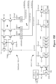
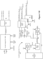
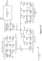
- FIGS 4A and 4B show an improved architecture 140 and ASIC 160 for an IPG such as IPG 10 described earlier. Elements in architecture 140 and ASIC 160 that can remain unchanged from the prior art architecture 40 and ASIC 60 described in the Introduction bear the same elements numerals, and are not described again.
- Improved ASIC 160 includes a microcontroller block 150 as part of its monolithic structure, which as shown in Figure 4B can communicate with other functional blocks in the ASIC 160 via internal bus 92. Because ASIC 160 includes an internal microcontroller 150, an external microcontroller (e.g., 50, Fig. 2A ) can be dispensed with in the improved architecture 140, simplifying IPG design and saving room within the interior of the case 12 and on the IPG's PCB 30 ( Fig. 1C ).
- an external microcontroller e.g., 50, Fig. 2A
- Microcontroller block 150 may receive interrupts independent of the bus 92 and its communication protocol, although interrupts may also be sent to the microcontroller 150 via the bus 92 as well. Even though ASIC 160 includes a microcontroller block 150, the ASIC 160 may still couple to an external bus 90, as shown in Figure 4A . This can facilitate communications between the ASIC 160 and another device, such as a memory integrated circuit (not shown) or possibly another microcontroller device that might be coupled to the bus 90. Bus 90 can also facilitate communication between (master) ASIC 160 and another identically-constructed (slave) ASIC 160', shown in dotted lines in Figure 4A . As described in the Introduction ( Fig.
- the microcontroller block 150 can comprise circuitry from an ARM Cortex-M0+ Processor, which may be incorporated into the monolithic integrated circuit of the ASIC 160 by licensing various necessary circuits from the library that comprises that processor.
- FIGs 5-13C describe details of improved stimulation circuitry 170, including improved DAC circuitry 172, within ASIC 160.
- Figure 5 shows a first example of DAC circuitry 172, in which each electrode node 61a (Ei) has its own dedicated PDAC (PDACi) able when selected to source a current to that electrode node, and its own dedicated NDAC (NDACi) able to sink a current from that electrode node.
- PDACi PDAC
- NDACi NDAC
- Each PDACi/NDACi pair outputs its current from output stages 183pi and 183ni respectively, the outputs of which are connected together at each electrode node Ei' (61a) to form a current Ii, which will source a current when the PDACi is active and sink a current when the NDACi is active.
- Output stages 183 in each PDAC and NDAC can be considered part of those PDACs and NDACs.
- Each electrode node Ei' is then preferably connected off chip to a DC-blocking capacitor Ci (55), which are then in turn connected to the lead-based electrodes Ei (16), as explained earlier.
- DAC circuitry 172 can further include passive recovery switches connected to each electrode node Ei' (96, Fig. 3 ), as is explained in further detail in U.S. Patent Application Publication 2018/0071527 .
- each of the PDACs, and the control signals they receive and process operate in a high power domain defined by power supply voltages VH and Vssh.
- VH comprises the compliance voltage described earlier and acts as the upper power supply within the high power domain, while Vssh is lower than VH and acts as the lower power supply within the high power domain.
- each of the NDACs, and the control signals they receive and process operate in a low power domain defined by power supply voltages Vcc and ground (GND; 0 Volts).
- Vcc acts as the upper power supply within the low power domain, while GND is lower than Vcc and acts as the lower power supply within the low power domain.
- Both of power supplies VH and Vssh are preferably variable as explained later, but are preferably higher than power supplies Vcc and ground.
- DAC circuitry 172 includes a master DAC (MDAC) 180 which communicates with all PDAC/NDAC pairs at each of the electrodes.
- Master DAC 180 receives an indication of the total anodic and total cathodic current amplitude 'A' of the stimulation pulses that the IPG will form at any given time, which indication is denoted by a bus of digital signals, ⁇ A>.
- the total anodic current sourced to the tissue should equal the total cathodic current sunk from the tissue at any point in time; otherwise an undesirable net charge would build in the patient's tissue.
- 'A' is the same for both total anodic current and total cathodic current.
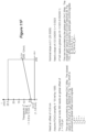
- Total anodic and cathodic current 'A' is illustrated by the example pulses in Figure 6 . Two sets of pulses are illustrated, and in each case, 'A' as set by amplitude bus ⁇ A> is 2 mA.
- ⁇ A> is 2 mA.
- PDAC3 simply sources +2 mA (the total anodic current) to its dedicated electrode E3 and to the patient's tissue Rt
- NDAC4 simply sinks -2 mA (the total cathodic current) from its dedicated electrode E4 and from the patient's tissue Rt.
- master DAC 180 in this example receives two reference currents, Iref_n and Iref_p of different polarities. This detail is explained later, but Iref_n and Iref_p are of essentially the same small magnitude, e.g., 100 nA, and both may therefore be simply referred to as Iref.
- the master DAC 180 amplifies the reference current by 'A' as specified by the amplitude bus ⁇ A>, and so outputs A*Iref. In the example shown, master DAC 180 outputs A*Iref with different polarities, again as explained later.
- ⁇ A> can comprise 8 bits, and thus master DAC 180 can output currents in 256 increments of Iref, i.e., 0, Iref, 2Iref, 3Iref, ... , 255Iref, or 0.0 nA, 100 nA, 200 nA, 300 nA, ... , 25.5 ⁇ A.
- the number of bits within amplitude bus ⁇ A> and hence the corresponding number of increments master DAC 180 can output are variable.
- A*Iref is further amplified at the PDACs or NDACs before being output to the electrode nodes 61a, as explained subsequently.
- Master DAC 180 provides A*Iref to distributor circuitry 182, whose function is to generate and distribute A*Iref to each PDAC and NDAC with the correct polarity. More specifically, and as the arrows in Figure 5 show, distributor 182 pulls A*Iref from the PDACs and pushes A*Iref to the NDACs.
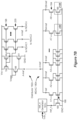
- Figures 7A and 7B show details of the master DAC 180 and distributor 182.
- the master DAC 180 comprises two sections 180p ( Fig. 7A ) and 180n ( Fig. 7B ).
- the distributor 182 also comprises two sections 182p ( Fig. 7A ) and 182n ( Fig. 7B ).
- Master DAC 180p and distributor 182p work together ( Fig. 7A ) to pull A*Iref from the PDACs, while master DAC 180n and distributor 182n work together ( Fig. 7B ) to push A*Iref to the NDACs.
- the circuitry 180p/182p and the circuitry of 180n/182n are symmetric, although 180p/182p are powered in the high power domain (VH/Vssh), while 180n/182n are powered in the low power domain (Vcc/GND). Further, the polarity of the transistors in 180p/182p and 180n/182n are different, with P-channel transistors proximate to the higher power supply in each power domain (VH and Vcc), and with N-channel transistors proximate to the lower power supply in each power domain (Vssh and GND).
- FIG. 7B shows master DAC 180n, which is controlled directly by the eight control signals A8:1 in amplitude bus ⁇ A>.
- Each of these control signals is input to a selection transistor 184, each of which is in series with a differing number of transistors 186 connected in parallel.
- Reference current Iref_n is produced by a generator 181n, and is provided to a transistor 185, which mirrors its current to each of the transistors 186. (Such mirroring occurs because the gates of transistor 185 and transistors 186 are connected to transistor 185's drain, as is well known).
- Master DAC 180n pulls output A*Iref from distributor 182n, which in turn pushes A*Iref out to each NDAC.
- A*Iref is mirrored into a series of branches each comprising a transistor 196 and a transistor 200 in series, with each branch pushing A*Iref to its dedicated NDAC.
- Distributor 182n is designed to achieve good linearity throughout the entire range with which A*Iref can vary (again, e.g., from 0 to 25.5 ⁇ A).
- Transistor 192 and transistors 196 form current mirrors, and are of the same size.
- Cascode transistors 198 and 200 are controlled by voltage Vcasc, and transistors 192, 194, 198, and 201 form a feedback loop.
- the master DAC 180p of Figure 7A operates similarly to push A*Iref to its distributor 182p, which in turn operates similarly to pull A*Iref from each of the PDACs.
- master DAC 180p includes its own generator 181p to generate its own reference current, Iref_p.
- Both the Iref_p generator 181p ( Fig. 7A ) and the Iref_n generator 181n ( Fig. 7B ) receive control signals Trim_p and Trim_n, which allow the magnitude of Iref_p and Iref_n to be adjusted.
- Iref_p and Iref_n are essentially the same magnitude (100 nA).
- Trim_p and Trim_n it is preferred to have the flexibility to adjust these magnitudes slightly via Trim_p and Trim_n to ensure that the amplified outputs A*Iref of the combinations 180p/182p and 180n/182n are equal; they might not be given non-idealities inherent in ASIC 160 fabrication. While reference current generation could be adjusted at any time, it is preferred to adjust Iref_p and Iref_n during manufacturing. For example, A*Iref can be measured during manufacturing from the master DAC 180p and the master DAC 180n, and Trim_p and Trim_n can be adjusted until the magnitude of A*Iref from each is equal. Thereafter, Trim_p and Trim_n can be stored in a non-volatile registers (not shown) so that generators 181p and 181n can output Iref_p and Iref_n with appropriate magnitudes.
- the master DAC 180 and distributor 182 will be located at a discrete location on the ASIC 160.
- each of the PDAC/NDAC pairs will be at different locations on the ASIC 160, such as generally proximate to the ASIC chip's bond pads (61) connected to electrode nodes Ei' 61a.
- This means the distance between the master DAC 180/distributor 182 and each PDAC/NDAC pair will vary. Nonetheless, because each PDAC and NDAC is current controlled (rather than voltage controlled)-i.e., controlled by A*Iref-such differences in distance are mitigated.
- each PDAC and NDAC will receive exactly A*Iref, allowing the PDACs and NDACs to output currents with proper amplitudes that do not vary as a function of their distance to the master DAC 180/distributor 182.
- Such current control of the PDACs and NDACs eases layout of the DAC circuitry 172 on the ASIC 160.
- percentage busses ⁇ X>, are shown, which are useful to allocating or "steering" of current between the electrodes, as explained further below.
- Each PDAC and NDAC receives its own percentage bus: thus, PDAC1 receives ⁇ Xp1>, NDAC1 receives ⁇ Xnl>, PDAC2 receives ⁇ Xp2>, NDAC2 receives ⁇ Xn2>, etc.
- the percentage busses ⁇ Xpi> specify a percentage (from 0-100%) of the total anodic current 'A' that each PDACi must source to its associated electrode node Ei'.
- Percentage busses ⁇ Xni> specify a percentage of the total cathodic current 'A' that each NDACi must sink from its associated electrode node Ei'.
- the various percentage busses ⁇ X> explain how the total anodic current and total cathodic current 'A' are shared between electrodes.
- amplitude 'A' is set by amplitude bus ⁇ A> to 2 mA in each example.
- amplitude bus ⁇ A> 100% of the total anodic and total cathodic current respectively. Therefore, percentage bus ⁇ Xp3> will indicate 100% to PDAC3 associated with electrode E3, and percentage bus ⁇ Xn4> will indicate 100% to NDAC4 associated with electrode E3.
- resolution control signals, K are shown.
- Each PDAC and NDAC preferably receives its own resolution control signal: thus, PDAC1 receives Kp1, NDAC1 receives Kn1, PDAC2 receives Kp2, NDAC2 receives Kn2, etc.
- the resolution control signals specify an amount by which each PDAC or NDAC's percentage (X) can be adjusted.
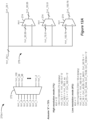
- the PDC operates to assert control signals to form pulses specified in the timing channels TC1-TC3, and may additionally take various actions to resolve conflicts where pulses in the various timing channels overlap in time, as discussed further below.
- the duration (D) and frequency of the pulses is generally set by the PDC by issuing the percentages busses and amplitudes at appropriate times.
- the pulses in TC1 and TC2 overlap.
- PDC in this example will need to provide a total anodic and cathodic amplitude sufficient to form the pulses in both timing channels. Because the pulses in TC1 require 3 mA and the pulses in TC2 require 2 mA, this totals 5 mA. However, the pulses in neither of these timing channels require the total 5 mA amplitude, meaning that the PDC must also adjust the percentage busses to ensure that pulses of proper amplitudes are formed. In other words, the PDC may adjust the percentage busses ⁇ Xi> from what they might otherwise be absent the overlap.
- PDC will provide percentage bus signals to PDAC and NDAC circuity involved in TC1 of 60 % (i.e., 3 mA/5 mA).
- ⁇ Xp1> signals for PDAC1 at electrode E1 60%
- ⁇ Xn2> signals for NDAC2 at electrode E2 60%
- PDC will provide percentage bus signals to PDAC and NDAC circuity involved in TC2 of 40 % (i.e., 2 mA/5 mA).
- ⁇ Xp3> signals for PDAC3 at electrode E3 equal 40%
- ⁇ Xn4> signals for NDAC4 at electrode E4 60%.
- the PDC may also address the possibility that a common electrode may be activated by more than one timing channel at a time.
- Time t0 illustrates such a conflict: as well as the pulses in timing channels overlapping at time t0, electrode E2 is active in both of timing channels TC1 and TC3. Further, notice that electrode E2 is simultaneously specified as a cathode (-3 mA) in TC1 and as an anode (+2 mA) in TC3.
- PDC may take different actions when such a conflict arises.
- PDC may, for example, simply apply arbitration rules to prevent the pulses in the timing channels from overlapping in time, for example, by issuing the pulses in TC2; then after the pulses in TC2 have finished, issuing the pulses in TC3; and then after the pulses in TC3 have finished, issuing the pulses in TC1.
- Such arbitration would resolve the conflict of E2 having to act as a cathode and anode simultaneously. See, e.g., U.S. Patent Application Publication 2013/0184794 (discussing arbitration of stimulation pulses in different timing channels).
- Exemplary values assist in understanding NDAC1's operation, and the magnitudes of the various currents it produces.
- the master DAC 180 in one example can output currents A*Iref of 100 nA, 200 nA, 300 nA, ... , 25.5 ⁇ A, depending on the value of the 'A' as set by amplitude bus ⁇ A>, and assuming a maximum value of 'A' of 255.
- the reference current (Iref), the maximum amount by which the reference current can be amplified by the master DAC 180 (A), the relative widths of the resistance transistor 252 and the branch transistors 254 (W1 and W2), or their relative resistance more generally, and the maximum number of branches (L) can all be adjusted in different designs.
- W2/W1 may even be less than one, meaning Ib would be smaller than A * Iref, which again may be considered as amplification.
- a large amount of current may be impractical: the compliance voltage VH may not be able to produce this, or the drain on the IPG's battery 14 may be too extreme. Such a large amount of current may also simply be unsafe.
- the total sourced or sunk current at any given time may be software limited to a more practical and safer value, such as 25.5 mA, even though such total value is below what the PDACs and NDACs together are capable of producing.
- Such limitation may be employed in software in the IPG 10 (in microcontroller block 150), or in the external controller used to program the IPG, that is, as a limitation constraining stimulation settings in the software of a clinician programmer or a hand-held patient programmer.
- MDAC 180 then generates an A*Iref current that is provided to a distributor 182 (182n and 182p), which delivers the A*Iref signal (with the appropriate polarity) to the NDACs and PDACs that produce the currents at the electrodes (e.g., E1).
- the NDACs and PDACs will amplify the received A*Iref current as explained above (e.g., by 1000) to produce the electrode currents.
- the NDAC and PDACs may also receive digital percentage control signals (e.g., ⁇ Xp1> and ⁇ Xn1>), which inform the NDACs and PDACs of a percentage of amplitude A that each should deliver. (How the percentage control signals ⁇ X> control the PDACs and NDACs to affect the current produced at each electrode is explained later with respect to Figures 12A-12C ).
- control signals 303ni allow A*Iref to be independently adjusted (e.g., to form A*G1*Iref+O1; A*G2*Iref+O2), thus allowing the NDACs at each electrode to receive independently-calibrated versions of the A*Iref current.
- the calibration circuits 302ni as described apply linear (i.e., gain and offset) compensation to the A*Iref signals, they may provide for non-linear compensation, including, for example, compensation based on higher order polynomials, exponential, logarithmic, or other suitable functions. See, e.g., U.S. Patent Application Publication 2021/0275798 (describing non-linear adjustment in an IPG's DAC circuitry).
- calibration circuits may be independent from the distributor circuitry as shown in Figure 10B , and thus the calibration circuits 302ni (302pi) may be interposed between the distributor 182n (182p) and the NDACs (or PDACs). Altematively, the calibration circuits 302ni (302pi) may be incorporated into the NDAC (or PDACs) at each electrode.
- the calibration circuits may comprise a modification to, or be incorporated within, the distributor circuity, and this is shown in Figure 10C.
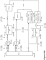
- Figure 10C shows the calibration circuit 302n1 that provides current to NDAC1 at electrode E1.
- This circuitry would be duplicated for other NDAC side calibration circuits, such as 302n2 that provides current to NDAC2 at electrode E2, etc., and would further be symmetrically duplicated (with polarities changes) for the PDAC side calibration circuits, such as 302p1 that provides current to PDAC1 at electrode E1, and 302p2 that provides current to PDAC2 at electrode E2, etc (see Fig. 10E ).
- calibration circuit 302n1 includes an electrode gain DAC 304, an electrode positive offset DAC 306p, and an electrode negative offset DAC 306n. Also shown in Figure 10C are aspects common to the NDAC side calibration circuits 302n1, including the MDAC 180n, which provides A*Iref to distributor 182n, and Iref generator 181n that provides Iref to the MDAC 180n (see Fig. 7B ). Notice that the Iref generator 181n also provides different polarities of Iref to the positive offset DAC 306p and the negative offset DAC 306n. A*Iref as before is provided to distributor 182n, namely into an input leg of a current mirror comprising transistors 192 and 198. Element 314 comprises a buffer.
- the gain DAC 304 includes output legs of the current mirror, and at least some of these legs are selectable to provide a current at node 325 which is supplied to NDAC1. In particular, certain output legs are selectable using gain control signals ⁇ Gn1>. Gain control signals ⁇ Gn1> comprise some of the control signals within control signals 303n1, as explained later with reference to Figure 10D . Notice that the output legs in the gain DAC 304 modify the non-selectable output legs (formed from transistors 196 and 200 in Fig. 7B ) used in the distributor 182n as described previously.
- Each output current leg in the gain DAC 304 includes in this example one or more parallel-connected mirror transistors 308, a cascode transistor 310, and a selection transistor 312. Similar to what was explained earlier, cascode transistors 198 and 310 are controlled by voltage Vcas0, but this detail is not important to understanding operation of the circuit.
- Current mirror transistors 308 produce a scalar of A*Iref provided to transistor 192, with the amount of current depending on the sizing of the transistor(s) 308 relative to transistor(s) 192, as well as the number of transistors that are provided in parallel both at 192 and 308.
- the other output legs in the gain DAC 304 have selection transistors 312 that are controlled by one of the gain control signals ⁇ Gn1>, of which there are five in this example (Gn1_0 to Gn1_4).
- each selectable leg includes a binary-weighted different number of paralleled current mirror transistors 308 (1, 2, 4, 8, and 16) to exponentially increase the amount of current these legs will carry.
- the first leg when selected by gain control signal Gn1_0 will carry approximately 0.0267*A*Iref (1*0.4/(3*5)); the second leg when selected by gain control signal Gn1_1 will carry approximately 0.0533*A*Iref ((2*0.4)/(3*5)); the third leg when selected by gain control signal Gn1_2 will carry approximately 0.107*A*Iref; the fourth leg when selected by gain control signal Gn1_3 will carry approximately 0.213*A*Iref; and the fifth leg when selected by gain control signal Gn1_4 will carry approximately 0.427* A*Iref.
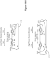
- gain DAC 304 allows the gain G of A*Iref to be adjusted from 0.8 to 1.627, which can be used to address a slope error in the electrode current, as occurs for electrodes E3, E4, and E5 in Figure 10A (301b).
- FIG. 10D summarizes the potential gains G in this example, and shows which of the gain control signals are asserted (+) or not asserted (-).
- signals will be asserted low if the gain DAC 304 comprises p-channel transistors, but would be asserted high when this DAC comprises n-channel transistors, as would be the case for the PDAC side calibration circuits 302pi).
- the gain G would be set to 1, requiring at least some of the gain control signals to be asserted (see decimal entries 7 or 8, each equally close to 1).
- the gain DAC 304 as described is just one example, and gain values producible by this DAC can be modified in other designs by changing the relative sizes and numbers of the transistors, the number of legs and gain control signals, etc.
- calibration circuit 302n1 also includes a positive offset DAC 306p and a negative offset DAC 306n either of which can be used to address an offset error, as occurs for electrodes E1, E2, and E5 in Figure 10A (301b). More specifically, for electrodes having a positive offset (e.g., E1, E5), a negative offset may be applied by the negative offset DAC 306n to "offset” this error. Similarly, for electrodes having a negative current offset error (e.g., E2), a positive offset may be applied by the positive offset DAC 306p to "offset" this error.
- a positive offset e.g., E2
- each of the offset DACs 306p and 306n may be constructed as binary-weighted current mirrors.
- the input leg of each DAC 306p/n includes an input transistor 322p/n and a corresponding cascode transistor 324p/n, with the input legs at the DACs receiving Iref with different polarities as shown.
- each offset DAC 306p and 306n is a three-bit DAC, with offset DAC 306p receiving offset control signals ⁇ OnP1> (OnP1_0, OnP1_1, and OnP1_2), and offset DAC 306n receiving offset control signals ⁇ OnN1> OnN1_0, OnN1_1, and OnN1_2).
- Offset control signals ⁇ OnP1> and ⁇ OnN1> comprise some of the control signals within control signals 303n1, as explained later with reference to Figure 10E .
- Positive offset control signals OnP1_0, OnP1_1, and OnP1_2 are applied to the gates of selection transistors 320p in the output legs of the DAC 306p to set a magnitude of a positive current offset (+O) at node 325.
- Negative offset control signals OnN1_0, OnN1_1, and OnN1_2 are similarly applied to the gates of selection transistors 320n in the output legs of the DAC 306n to set a magnitude of a negative current offset (-O) at node 325.
- This drive arrangement thus requires a total of six bits, but this could also be modified. For example, four bits could also be used: one bit to select either of the offset DACs 306p or 306n, and three bits to set the offset magnitude O.
- the output legs of the offset DACs 306p/n include three transistors: current mirror transistors 316p/n, cascode transistors 318p/n, and the selection transistors 320p/n.
- the transistors used to form the input transistors 322p/n and the current mirror transistors 316p/n are sized the same, and thus each output leg will form a scalar of Iref in accordance with the different number of paralleled transistors provided for each. In this example, there are two paralleled transistors for the input transistors 322p/n.
- the currents provided to each electrode's NDAC and PDAC are independently calibrated, thus calibrating each electrode's current whether it is acting as an anode to source current or a cathode to sink current.
- Non-ideal currents may result from non-idealities in A*Iref as produced and distributed (e.g., by MDAC 180 and distributor 182), or in the PDAC or NDACs themselves (which as discussed earlier can amplify the received A*Iref current to produce larger currents at the electrodes).
- the global offset DAC 365p should produce.
- the closest current to this value the DAC 356p can produce is 4 ⁇ A (decimal 4), which is formed by asserting only global offset control signal ⁇ _2 ( ⁇ _4, ⁇ _3, ⁇ _1, and ⁇ _0 are not asserted) in the global offset DAC 356p.
- the global gain value B to be provided by global gain DAC 354p is assessed.
- a global current memory 410 can store values for the global gain (B) and the global offset ( ⁇ ), as reflected by control signals ⁇ B> and ⁇ >, which relevant control circuitry in the ASIC 160 (such as the Pulse Definition Circuit (PDC) ( Fig. 8A ) or the microcontroller block 150 ( Fig. 4B ) can read.
- the values for the global gain B and global offset ⁇ are preferably the same on both the NDAC side and the PDAC side to ensure that electrode currents are of uniform magnitudes regardless of polarity.
- Figure 11H shows another alternative in which a single current range DAC 400 is used to service both the NDAC and PDAC sides of the DAC circuitry.
- This current is in tum provided to a polarity circuit 450 that produces the current with this magnitude and with the proper polarity to be received by distributor 182n on the NDAC side and distributor 182p on the PDAC side as shown.
- GUI graphical user interface
- a global gain and offset algorithm 440 operable in the external device may then compute the global gain (B) and global offset ( ⁇ ) values, and the relevant control signals ⁇ B> and ⁇ >, needed to provide for control over the entire range of amplitude values, and to provide those to the DAC circuit 172 in the IPG (for storage in global current memory 410).
- the GUI 420 may also allow the current to be adjusted within the therapeutic range established by B and A.
- the GUI 420 can show an amplitude I (e.g., 5.9 mA) to which the IPG is presently programmed, and can provide one or more inputs 460 to allow the amplitude to be increased (+) or decreased (-).
- I e.g., 5.9 mA
- Other GUI schemes can be used to adjust the amplitude, such as those described in U.S. Patent Application Publication 2021/0299457 .
- the amplitude within the therapeutic range can also be expressed more qualitatively.
- the amplitude may be expressed in terms of a percentage (e.g., 26%), which indicates for the user a general intensity of the amplitude within the therapeutic range (e.g., 5.9 mA is 26% of the way between 3.8 mA and 12 mA).
- a percentage e.g., 26%)
- 5.9 mA is 26% of the way between 3.8 mA and 12 mA.
- Other GUI schemes may be used to qualitatively indicate a presently-programmed amplitude within the therapeutic range.
- the resolution mode affects how the percentage 'X' can be incremented or decremented in a DAC, which is constrained by the number of branches that the logic circuitry 270 can turn on in each mode. Assume for example that 'X' is incremented from 4% in Figure 12B . If the PDC specifies that the DAC at issue operates in the high resolution mode, incrementing 'X' means that X will now equal 5%, because 'X' can be incremented in 1% steps.
- each of the DAC's branches are asserted/unasserted one at a time when 'X' is incremented/decremented, and in physical order in the DAC.
- the logic circuitry 270 in effect ties switch control signals Ci, C(i+25), C(i+50), and C(i+75) together, thus permitting only groups of 4 branches (in physically different locations) to be chosen.
- switch control signals C100:1 are not sent to sequentially physical branches in the DAC as in the illustrated examples, different physical branches would be selected to contribute to the current the DAC produces.
- Logic circuitry 270 includes a first multiplexer stage 276 essentially similar to that described earlier, except that it is not enabled in the medium resolution mode.
- Thermometer decoder 272 ( Fig. 12A ) would assert intermediate signals Y36:1, which multiplexer 278 in second multiplexer stage 277 would pass to both C36:1 and C86:51.
- DAC branches would be asserted two at a time (C1 and C51, C2 and C52, etc.), thus providing 2% increments of amplitude 'A' to be output by the DAC.
- This is just one example in which a multi-resolution mode could be implemented, and other examples are possible.
- the percentage busses ⁇ X> provide a convenient way to "steer" current between different electrodes. Steering involves moving some portion of anodic current between two or more electrodes, or moving some portion of cathodic current between two or more electrodes.
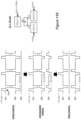
- An example of current steering is shown in Figure 13A , which involves use of electrode E1 as an anode, and electrodes E2 and E3 as cathodes (during first pulse phases 94a).
- cathodic current (-10 mA) is steered from E2 to E3 in gradual increments: initially, the entirety of the cathodic current is placed on E2, but eventually at the end of steering the entirety of the cathodic current is placed on E3.
- An intermediate setting is shown during the steering process at which the cathodic current at electrodes E2 and E3 are roughly equal (-5.2 mA and -4.8 mA).
- the anodic current issued from E1 stays constant (+10 mA), but anodic current may also be steered to and from different electrodes in more complicated examples.
- Steering current between electrodes in small increments is a desirable use model, particularly during fitting of the IPG 10 to a particular patient. This because it may not initially be known what electrodes should be chosen for stimulation to relieve a patient's symptoms (e.g., pain). Gradually moving current between electrodes to determine which electrodes should be active to provide therapy, and in what proportions, may be more comfortable and less dangerous for the patient. For example, if all of the cathodic current is moved instantaneously from E2 to E3 in the example of Figure 13A (from the initial setting to the final setting), the effect may be jarring on the patient.
- Moving current in gradual increments reduces this risk, and allows finer tuning of therapy as source current can be shared by one or more selected anode electrodes, and sink current can be shared by one or more selected cathode electrodes. See USP 7,890,182 , discussing this issue in further detail.
- Moving current in the manner shown can be performed by a clinician programmer running IPG control software in communication with a patient's IPG 10.
- current may also be movable between electrodes by the patient using a hand-holdable external controller.
- the current may be moved automatically by the IPG 10, i.e., by the microcontroller block 150 or the PDC (see Fig. 8A ).
- Figures 13B and 13C shows how steering current between the electrodes E2 and E3 of Figure 13A can be achieved using DAC circuitry 172, in high and low resolution modes respectively.
- amplitude bus ⁇ A> sets a value 'A' of 10 mA-the total anodic and cathodic current required.
- percentage bus ⁇ Xp1> 100%, because all anodic current will be provided by PDAC1 associated with electrode E1.
- Bus ⁇ Xn1> 0%, because E1 is not acting as a cathode, and thus NDAC1 will be inactive.
- busses ⁇ Xp2> and ⁇ Xp3> 0% because electrodes E2 and E3 are not acting as anodes, and thus PDAC2 and PDAC3 will be inactive.
- all other percentage busses ⁇ Xp4>, ⁇ Xn4>, ⁇ Xp5>, ⁇ Xn5>, ... , ⁇ Xp16>, ⁇ Xn16>, ⁇ Xpc>, Xnc>) are set to 0%, because electrodes E4-E16 and Ec are not selected for stimulation, and hence their PDACs and NDACs are inactive.
- Figure 13B illustrates steering in the high resolution mode.
- Each 1% adjustment occurs at sequential times t0, t1, t2, ... , t100, which adjustments can again be made using a clinician programmer or patient external controller, and wirelessly transmitted to the IPG 10.
- PDC sets ⁇ Xn2> to 100%, and thus logic circuitry 270 ( Fig.
Landscapes
- Health & Medical Sciences (AREA)
- Engineering & Computer Science (AREA)
- Biomedical Technology (AREA)
- Nuclear Medicine, Radiotherapy & Molecular Imaging (AREA)
- Radiology & Medical Imaging (AREA)
- Life Sciences & Earth Sciences (AREA)
- Animal Behavior & Ethology (AREA)
- General Health & Medical Sciences (AREA)
- Public Health (AREA)
- Veterinary Medicine (AREA)
- Physics & Mathematics (AREA)
- Nonlinear Science (AREA)
- Theoretical Computer Science (AREA)
- Electrotherapy Devices (AREA)
Claims (15)
- Impulsgenerator (10), aufweisend:eine Mehrzahl von Elektrodenknoten (61a), wobei jeder Elektrodenknoten dafür konfiguriert ist, mit einer Elektrode (16) verbunden zu werden, die dafür konfiguriert ist, mit Gewebe eines Patienten in Kontakt zu kommen;einen ersten Digital-Analog-Wandler, DAC, der dafür konfiguriert ist, digitale Daten zu empfangen, die eine Größe einer an den Elektrodenknoten zu erzeugenden Gesamtanodenstromamplitude angeben, und einen ersten Strom mit einer Größe zu erzeugen, die die Gesamtanodenstromamplitude anzeigt;mehrere erste Kalibrierschaltungen, die jeweils dafür konfiguriert sind, den ersten Strom zu empfangen, wobei jede der ersten Kalibrierschaltungen derart steuerbar ist, dass sie als Funktion des ersten Stroms einen unterschiedlichen zweiten Strom erzeugt; undmehrere zweite DACs, die jeweils einem der Elektrodenknoten zugeordnet sind, wobei jeder zweite DAC dafür konfiguriert ist, einen der zweiten Ströme zu empfangen, wobei jeder der zweiten DACs derart konfiguriert ist, dass er, wenn er ausgewählt ist, seinen empfangenen zweiten Strom verstärkt, um einen anodischen Stimulationsstrom an seinem zugeordneten Elektrodenknoten zu erzeugen.
- Impulsgenerator nach Anspruch 1, wobei jede der ersten Kalibrierschaltungen derart steuerbar ist, dass sie ihren zweiten Strom als eine lineare Funktion des ersten Stroms erzeugt.
- Impulsgenerator nach Anspruch 2, wobei jede der ersten Kalibrierschaltungen derart steuerbar ist, dass sie bei Erzeugung ihres zweiten Stroms eine Verstärkung und/oder einen Offset für den ersten Strom bereitstellt.
- Impulsgenerator nach einem der Ansprüche 1 bis 3, wobei jede der ersten Kalibrierschaltungen unabhängig über eindeutige erste Steuersignale, die an jeder ersten Kalibrierschaltung empfangen werden, derart steuerbar ist, dass sie ihren zweiten Strom erzeugt.
- Impulsgenerator nach einem der Ansprüche 1 bis 4, wobei jede der ersten Kalibrierschaltungen einen Gain-DAC aufweist, der dafür konfiguriert ist, dem ersten Strom bei Erzeugung seines zweiten Stroms eine Verstärkung aufzuprägen.
- Impulsgenerator nach einem der Ansprüche 1 bis 5, wobei jede der ersten Kalibrierschaltungen einen Offset-DAC aufweist, der dafür konfiguriert ist, dem ersten Strom bei Erzeugung seines zweiten Stroms einen Offset aufzuprägen.
- Impulsgenerator nach einem der Ansprüche 1 bis 6, wobei der erste DAC dafür konfiguriert ist, einen Referenzstrom zu empfangen, wobei die Größe des ersten Stroms einen Skalar des Referenzstroms aufweist.
- Impulsgenerator nach Anspruch 7, wobei jede der ersten Kalibrierschaltungen einen Offset-DAC aufweist, der dafür konfiguriert ist, dem ersten Strom bei der Erzeugung seines zweiten Stroms einen Offset aufzuprägen, wobei jeder der Offset-DACs dafür konfiguriert ist, den Referenzstrom zu empfangen, wobei der Offset einen Skalar des Referenzstroms aufweist.
- Impulsgenerator nach einem der Ansprüche 1 bis 5, wobei jede der ersten Kalibrierschaltungen einen Gain-DAC aufweist, der dafür konfiguriert ist, dem ersten Strom bei der Erzeugung seines zweiten Stroms eine Verstärkung aufzuprägen, und wobei jede der ersten Kalibrierschaltungen einen Offset-DAC aufweist, der dafür konfiguriert ist, dem ersten Strom bei der Erzeugung seines zweiten Stroms einen Offset aufzuprägen.
- Impulsgenerator nach einem der Ansprüche 1 bis 9, wobei die Summe der anodischen Stimulationsströme an den Elektrodenknoten der Gesamtanodenstromamplitude gleicht.
- Impulsgenerator nach einem der Ansprüche 1 bis 10, wobei die digitalen Daten ferner eine Größe einer an den Elektrodenknoten zu erzeugenden Gesamtkathodenstromamplitude spezifizieren, wobei der erste DAC ferner dafür konfiguriert ist, einen dritten Strom mit einer Größe zu erzeugen, die die an den Elektrodenknoten zu erzeugende Gesamtkathodenstromamplitude anzeigt, wobei eine Polarität des dritten Stroms derjenigen des ersten Stroms entgegengesetzt ist, und wobei der Impulsgenerator ferner aufweist:eine Mehrzahl von zweiten Kalibrierschaltungen, die jeweils dafür konfiguriert sind, den dritten Strom zu empfangen, wobei jede der zweiten Kalibrierschaltungen derart steuerbar ist, dass sie einen unterschiedlichen vierten Strom als Funktion des dritten Stroms erzeugt; undeine Mehrzahl von dritten DACs, die jeweils einem der Elektrodenknoten zugeordnet sind, wobei jeder dritte DAC dafür konfiguriert ist, einen der vierten Ströme zu empfangen, wobei jeder der dritten DACs dafür konfiguriert ist, wenn er ausgewählt ist, seinen empfangenen vierten Strom zu verstärken, um einen kathodischen Stimulationsstrom an seinem zugehörigen Elektrodenknoten zu erzeugen.
- Impulsgenerator nach Anspruch 11, wobei jede der zweiten Kalibrierschaltungen derart steuerbar ist, dass sie ihren vierten Strom als eine lineare Funktion des dritten Stroms erzeugt.
- Impulsgenerator nach Anspruch 11 oder 12, wobei jede der zweiten Kalibrierschaltungen unabhängig über eindeutige zweite Steuersignale, die an jeder zweiten Kalibrierschaltung empfangen werden, steuerbar ist, um ihren vierten Strom zu erzeugen.
- Impulsgenerator nach einem der Ansprüche 11 bis 13, wobei jede der zweiten Kalibrierschaltungen einen Gain-DAC aufweist, der dafür konfiguriert ist, dem dritten Strom bei der Erzeugung seines vierten Stroms eine Verstärkung aufzuprägen, und wobei jede der zweiten Kalibrierschaltungen einen Offset-DAC aufweist, der dafür konfiguriert ist, dem dritten Strom bei der Erzeugung seines vierten Stroms einen Offset aufzuprägen.
- Impulsgenerator nach einem der Ansprüche 11 bis 14, wobei die Summe der kathodischen Stimulationsströme an den Elektrodenknoten der Gesamtkathodenstromamplitude gleicht, und wobei die Summe der anodischen Stimulationsströme an den Elektrodenknoten der Summe der kathodischen Stimulationsströme an den Elektrodenknoten gleicht.
Priority Applications (1)
| Application Number | Priority Date | Filing Date | Title |
|---|---|---|---|
| EP25176400.7A EP4599883A3 (de) | 2021-04-06 | 2022-03-10 | Stromerzeugungarchitektur für eine implantierbare stimulatorvorrichtung |
Applications Claiming Priority (2)
| Application Number | Priority Date | Filing Date | Title |
|---|---|---|---|
| US202163171329P | 2021-04-06 | 2021-04-06 | |
| PCT/US2022/071074 WO2022217184A1 (en) | 2021-04-06 | 2022-03-10 | Current generation architecture for an implantable stimulator device |
Related Child Applications (2)
| Application Number | Title | Priority Date | Filing Date |
|---|---|---|---|
| EP25176400.7A Division EP4599883A3 (de) | 2021-04-06 | 2022-03-10 | Stromerzeugungarchitektur für eine implantierbare stimulatorvorrichtung |
| EP25176400.7A Division-Into EP4599883A3 (de) | 2021-04-06 | 2022-03-10 | Stromerzeugungarchitektur für eine implantierbare stimulatorvorrichtung |
Publications (2)
| Publication Number | Publication Date |
|---|---|
| EP4284487A1 EP4284487A1 (de) | 2023-12-06 |
| EP4284487B1 true EP4284487B1 (de) | 2025-07-02 |
Family
ID=80999184
Family Applications (2)
| Application Number | Title | Priority Date | Filing Date |
|---|---|---|---|
| EP22714096.9A Active EP4284487B1 (de) | 2021-04-06 | 2022-03-10 | Stromerzeugungarchitektur für eine implantierbare stimulatorvorrichtung |
| EP25176400.7A Pending EP4599883A3 (de) | 2021-04-06 | 2022-03-10 | Stromerzeugungarchitektur für eine implantierbare stimulatorvorrichtung |
Family Applications After (1)
| Application Number | Title | Priority Date | Filing Date |
|---|---|---|---|
| EP25176400.7A Pending EP4599883A3 (de) | 2021-04-06 | 2022-03-10 | Stromerzeugungarchitektur für eine implantierbare stimulatorvorrichtung |
Country Status (3)
| Country | Link |
|---|---|
| US (2) | US11967969B2 (de) |
| EP (2) | EP4284487B1 (de) |
| WO (1) | WO2022217184A1 (de) |
Families Citing this family (1)
| Publication number | Priority date | Publication date | Assignee | Title |
|---|---|---|---|---|
| CN120357904B (zh) * | 2025-06-25 | 2025-09-12 | 成都市晶蓉微电子有限公司 | 一种低功耗Sigma-Delta调制器 |
Family Cites Families (64)
| Publication number | Priority date | Publication date | Assignee | Title |
|---|---|---|---|---|
| AU4959799A (en) | 1998-06-26 | 2000-01-17 | Advanced Bionics Corporation | Programmable current output stimulus stage for implantable device |
| US6516227B1 (en) | 1999-07-27 | 2003-02-04 | Advanced Bionics Corporation | Rechargeable spinal cord stimulator system |
| US6553263B1 (en) | 1999-07-30 | 2003-04-22 | Advanced Bionics Corporation | Implantable pulse generators using rechargeable zero-volt technology lithium-ion batteries |
| US6466822B1 (en) | 2000-04-05 | 2002-10-15 | Neuropace, Inc. | Multimodal neurostimulator and process of using it |
| US6993384B2 (en) | 2001-12-04 | 2006-01-31 | Advanced Bionics Corporation | Apparatus and method for determining the relative position and orientation of neurostimulation leads |
| US20030153959A1 (en) | 2002-02-12 | 2003-08-14 | Thacker James R. | Neural stimulation system providing auto adjustment of stimulus output as a function of sensed coupling efficiency |
| WO2004002572A1 (en) | 2002-06-28 | 2004-01-08 | Advanced Bionics Corporation | Microstimulator having self-contained power source and bi-directional telemetry system |
| US7127298B1 (en) | 2002-10-18 | 2006-10-24 | Advanced Bionics Corporation | Switched-matrix output for multi-channel implantable stimulator |
| US7539538B2 (en) | 2004-05-28 | 2009-05-26 | Boston Science Neuromodulation Corporation | Low power loss current digital-to-analog converter used in an implantable pulse generator |
| US20060173493A1 (en) | 2005-01-28 | 2006-08-03 | Cyberonics, Inc. | Multi-phasic signal for stimulation by an implantable device |
| US7801602B2 (en) | 2005-04-08 | 2010-09-21 | Boston Scientific Neuromodulation Corporation | Controlling stimulation parameters of implanted tissue stimulators |
| US7801600B1 (en) | 2005-05-26 | 2010-09-21 | Boston Scientific Neuromodulation Corporation | Controlling charge flow in the electrical stimulation of tissue |
| US8620436B2 (en) | 2005-07-08 | 2013-12-31 | Boston Scientific Neuromodulation Corporation | Current generation architecture for an implantable stimulator device having coarse and fine current control |
| US8606362B2 (en) | 2005-07-08 | 2013-12-10 | Boston Scientific Neuromodulation Corporation | Current output architecture for an implantable stimulator device |
| US7872884B2 (en) | 2005-11-03 | 2011-01-18 | Boston Scientific Neuromodulation Corporation | Cascaded step-up converter and charge pump for efficient compliance voltage generation in an implantable stimulator device |
| US7444181B2 (en) | 2005-12-14 | 2008-10-28 | Boston Scientific Neuromodulation Corporation | Techniques for sensing and adjusting a compliance voltage in an implantable stimulator device |
| US7881803B2 (en) | 2006-10-18 | 2011-02-01 | Boston Scientific Neuromodulation Corporation | Multi-electrode implantable stimulator device with a single current path decoupling capacitor |
| US7623916B2 (en) | 2006-12-20 | 2009-11-24 | Cameron Health, Inc. | Implantable cardiac stimulus devices and methods with input recharge circuitry |
| US8649858B2 (en) | 2007-06-25 | 2014-02-11 | Boston Scientific Neuromodulation Corporation | Architectures for an implantable medical device system |
| US7890182B2 (en) | 2008-05-15 | 2011-02-15 | Boston Scientific Neuromodulation Corporation | Current steering for an implantable stimulator device involving fractionalized stimulation pulses |
| US9987493B2 (en) | 2008-10-28 | 2018-06-05 | Medtronic, Inc. | Medical devices and methods for delivery of current-based electrical stimulation therapy |
| US9233254B2 (en) | 2009-02-17 | 2016-01-12 | Boston Scientific Neuromodulation Corporation | Selectable boost converter and charge pump for compliance voltage generation in an implantable stimulator device |
| US20100268309A1 (en) | 2009-04-17 | 2010-10-21 | Boston Scientific Neuromodulation Corporation | Architectures for Multi-Electrode Implantable Stimulator Devices Having Minimal Numbers of Decoupling Capacitors |
| CA2785799A1 (en) | 2009-12-30 | 2011-07-07 | Boston Scientific Neuromodulation Corporation | System and method for independently operating multiple neurostimulation channels |
| US9020589B2 (en) | 2010-04-27 | 2015-04-28 | Medtronic, Inc. | Electrical stimulator with voltage mode emulation using regulated current |
| US9155891B2 (en) | 2010-09-20 | 2015-10-13 | Neuropace, Inc. | Current management system for a stimulation output stage of an implantable neurostimulation system |
| CA2921986A1 (en) | 2010-10-13 | 2012-04-19 | Boston Scientific Neuromodulation Corporation | Architectures for an implantable medical device system having daisy-chained electrode-driver integrated circuits |
| US8768453B2 (en) | 2010-10-13 | 2014-07-01 | Boston Scientific Neuromodulation Corporation | Monitoring electrode voltages in an implantable medical device system having daisy-chained electrode-driver integrated circuits |
| US9061140B2 (en) | 2010-10-13 | 2015-06-23 | Boston Scientific Neuromodulation Corporation | Sample and hold circuitry for monitoring voltages in an implantable neurostimulator |
| AU2011329370B2 (en) | 2010-11-17 | 2014-11-20 | Boston Scientific Neuromodulation Corporation | External trial stimulator useable in an implantable neurostimulator system |
| US9308373B2 (en) | 2011-06-29 | 2016-04-12 | Boston Scientific Neuromodulation Corporation | Architectures for sharing of current sources in an implantable medical device |
| US20130184794A1 (en) | 2012-01-16 | 2013-07-18 | Boston Scientific Neuromodulation Corporation | Architectures for an Implantable Stimulator Device Having a Plurality of Electrode Driver Integrated Circuits with Shorted Electrode Outputs |
| US9037241B2 (en) | 2012-02-10 | 2015-05-19 | Boston Scientific Neuromodulation Corporation | Power architecture for an implantable medical device having a non-rechargeable battery |
| US9352162B2 (en) | 2012-02-10 | 2016-05-31 | Boston Scientific Neuromodulation Corporation | Power architecture for an implantable medical device having a non-rechargeable battery |
| CN104168949B (zh) | 2012-03-16 | 2016-08-24 | 波士顿科学神经调制公司 | 用于防止电子电路中磁感生电流的神经刺激系统 |
| US9002465B2 (en) | 2012-04-06 | 2015-04-07 | Boston Scientific Neuromodulation Corporation | Verifying correct operation of an implantable neurostimulator device using current distribution circuitry |
| AU2013252839B2 (en) | 2012-04-27 | 2015-09-17 | Boston Scientific Neuromodulation Corporation | Timing channel circuitry for creating pulses in an implantable stimulator device |
| US9174051B2 (en) | 2012-04-29 | 2015-11-03 | Boston Scientific Neuromodulation Corporation | Real time compliance voltage generation for an implantable stimulator |
| US9314632B2 (en) | 2012-05-17 | 2016-04-19 | Boston Scientific Neuromodulation Corporation | Pulse-by-pulse compliance voltage generation for an implantable stimulator |
| US9397639B2 (en) | 2013-03-14 | 2016-07-19 | Boston Scientific Neuromodulation Corporation | Integrated circuitry for generating a clock signal in an implantable medical device |
| EP2974016B1 (de) | 2013-03-15 | 2019-03-06 | Alfred E. Mann Foundation for Scientific Research | Strommessung mit mehreren ausgangsstromstimulatoren mit schneller einschaltzeit |
| US9327135B2 (en) | 2013-06-04 | 2016-05-03 | Boston Scientific Neuromodulation Corporation | External device for determining an optimal implantable medical device for a patient using information determined during an external trial stimulation phase |
| US9861825B2 (en) | 2013-11-08 | 2018-01-09 | Boston Scientific Neuromodulation Corporation | Orientation and placement of inductive components to minimize noise coupling to a communication coil in an implantable medical device |
| KR101627204B1 (ko) | 2013-11-28 | 2016-06-03 | 엘지전자 주식회사 | 태양 전지 및 이의 제조 방법 |
| US9713717B2 (en) | 2013-12-09 | 2017-07-25 | Boston Scientific Neuromodulation Corporation | Implantable stimulator device having components embedded in a circuit board |
| EP3708218A1 (de) | 2014-06-21 | 2020-09-16 | Nalu Medical, Inc. | Vorrichtung für neuromodulationsbehandlungen von schmerzen und anderen störungen |
| EP3791922B1 (de) | 2014-07-10 | 2025-04-02 | Curonix LLC | Schaltung für eine implantierbare vorrichtung |
| US9533162B2 (en) | 2014-08-21 | 2017-01-03 | Boston Scientific Neuromodulation Corporation | Use of a dedicated remote control as an intermediary device to communicate with an implantable medical device |
| US10716937B2 (en) | 2016-09-10 | 2020-07-21 | Boston Scientific Neuromodulation Corporation | Passive charge recovery circuitry for an implantable medical device |
| US20180071515A1 (en) | 2016-09-10 | 2018-03-15 | Boston Scientific Neuromodulation Corporation | Pulse Definition Circuitry for Creating Stimulation Waveforms in an Implantable Pulse Generator |
| US10716932B2 (en) | 2016-09-10 | 2020-07-21 | Boston Scientific Neuromodulation Corporation | Pulse definition circuitry for creating stimulation waveforms in an implantable pulse generator |
| US10576265B2 (en) | 2016-09-10 | 2020-03-03 | Boston Scientific Neuromodulation Corporation | Pulse definition circuitry for creating stimulation waveforms in an implantable pulse generator |
| US11040192B2 (en) | 2016-09-10 | 2021-06-22 | Boston Scientific Neuromodulation Corporation | Current generation architecture for an implantable medical device |
| US10786665B2 (en) | 2016-09-10 | 2020-09-29 | Boston Scientific Neuromodulation Corporation | Biasing of a current generation architecture for an implantable medical device |
| US10716941B2 (en) | 2017-01-06 | 2020-07-21 | Regents Of The University Of Minnesota | System and method for charge-balancing neurostimulator with neural recording |
| NL2019707B1 (en) * | 2017-10-11 | 2019-04-19 | Boston Scient Neuromodulation Corp | Current Generation Architecture for an Implantable Stimulator Device to Promote Current Steering Between Electrodes |
| AU2018222994B2 (en) | 2017-09-15 | 2019-11-07 | Boston Scientific Neuromodulation Corporation | Current generation architecture for an implantable stimulator device to promote current steering between electrodes |
| ES2925235T3 (es) * | 2017-09-15 | 2022-10-14 | Boston Scient Neuromodulation Corp | Arquitectura de generación de corriente para un dispositivo estimulador implantable que incluye circuitos distribuidores para enviar una corriente de amplitud escalada a convertidores de digital a analógico en los electrodos |
| EP3765145B1 (de) | 2018-03-12 | 2024-04-24 | Boston Scientific Neuromodulation Corporation | Neurale stimulation basierend auf zerlegung der evozierten summenaktionspotenziale |
| US11040202B2 (en) | 2018-03-30 | 2021-06-22 | Boston Scientific Neuromodulation Corporation | Circuitry to assist with neural sensing in an implantable stimulator device |
| EP4282467B1 (de) | 2019-07-02 | 2025-08-27 | Boston Scientific Neuromodulation Corporation | System zur stimulation des rückenmarks, das die optimale sub-perzeptionstherapie unter verwendung der nervendosis bestimmt |
| WO2021119741A1 (en) | 2019-12-17 | 2021-06-24 | The Bionics Institute Of Australia | Methods and system for modulating glycaemia |
| EP4114511B1 (de) | 2020-03-03 | 2025-06-18 | Boston Scientific Neuromodulation Corporation | Digital-analog-wandlerschaltung für eine stimulatorvorrichtung mit nichtlinearer amplitudeneinstellung |
| EP4072661A1 (de) | 2020-03-26 | 2022-10-19 | Boston Scientific Neuromodulation Corporation | Grafische benutzerschnittstelle zum einstellen der aktuellen grösse in einer stimulatorvorrichtung |
-
2022
- 2022-03-10 EP EP22714096.9A patent/EP4284487B1/de active Active
- 2022-03-10 WO PCT/US2022/071074 patent/WO2022217184A1/en not_active Ceased
- 2022-03-10 EP EP25176400.7A patent/EP4599883A3/de active Pending
- 2022-03-10 US US17/654,345 patent/US11967969B2/en active Active
-
2024
- 2024-03-20 US US18/611,399 patent/US12231139B2/en active Active
Also Published As
| Publication number | Publication date |
|---|---|
| US20220321139A1 (en) | 2022-10-06 |
| WO2022217184A1 (en) | 2022-10-13 |
| EP4599883A3 (de) | 2025-11-05 |
| US12231139B2 (en) | 2025-02-18 |
| EP4599883A2 (de) | 2025-08-13 |
| US20240235568A1 (en) | 2024-07-11 |
| EP4284487A1 (de) | 2023-12-06 |
| US11967969B2 (en) | 2024-04-23 |
Similar Documents
| Publication | Publication Date | Title |
|---|---|---|
| US11697021B2 (en) | Current generation architecture for an implantable stimulator device to promote current steering between electrodes | |
| US11998732B2 (en) | Current generation architecture for an implantable medical device | |
| US10786665B2 (en) | Biasing of a current generation architecture for an implantable medical device | |
| EP3639887B1 (de) | Stromgeneratorarchitektur für einen implantierbaren stimulator zur förderung der stromsteuerung zwischen den elektroden | |
| US12231139B2 (en) | Current generation architecture for an implantable stimulator device | |
| US20230347157A1 (en) | Current Generation Architecture for an Implantable Stimulator Device Including Distributor Circuitry for Sending an Amplitude-Scaled Current to Digital-to-Analog Converters at the Electrodes | |
| US10549091B2 (en) | Use models for a current generation architecture for an implantable medical device |
Legal Events
| Date | Code | Title | Description |
|---|---|---|---|
| STAA | Information on the status of an ep patent application or granted ep patent |
Free format text: STATUS: UNKNOWN |
|
| STAA | Information on the status of an ep patent application or granted ep patent |
Free format text: STATUS: THE INTERNATIONAL PUBLICATION HAS BEEN MADE |
|
| PUAI | Public reference made under article 153(3) epc to a published international application that has entered the european phase |
Free format text: ORIGINAL CODE: 0009012 |
|
| STAA | Information on the status of an ep patent application or granted ep patent |
Free format text: STATUS: REQUEST FOR EXAMINATION WAS MADE |
|
| 17P | Request for examination filed |
Effective date: 20230830 |
|
| AK | Designated contracting states |
Kind code of ref document: A1 Designated state(s): AL AT BE BG CH CY CZ DE DK EE ES FI FR GB GR HR HU IE IS IT LI LT LU LV MC MK MT NL NO PL PT RO RS SE SI SK SM TR |
|
| DAV | Request for validation of the european patent (deleted) | ||
| DAX | Request for extension of the european patent (deleted) | ||
| GRAP | Despatch of communication of intention to grant a patent |
Free format text: ORIGINAL CODE: EPIDOSNIGR1 |
|
| STAA | Information on the status of an ep patent application or granted ep patent |
Free format text: STATUS: GRANT OF PATENT IS INTENDED |
|
| INTG | Intention to grant announced |
Effective date: 20250129 |
|
| GRAS | Grant fee paid |
Free format text: ORIGINAL CODE: EPIDOSNIGR3 |
|
| GRAA | (expected) grant |
Free format text: ORIGINAL CODE: 0009210 |
|
| STAA | Information on the status of an ep patent application or granted ep patent |
Free format text: STATUS: THE PATENT HAS BEEN GRANTED |
|
| AK | Designated contracting states |
Kind code of ref document: B1 Designated state(s): AL AT BE BG CH CY CZ DE DK EE ES FI FR GB GR HR HU IE IS IT LI LT LU LV MC MK MT NL NO PL PT RO RS SE SI SK SM TR |
|
| REG | Reference to a national code |
Ref country code: GB Ref legal event code: FG4D |
|
| REG | Reference to a national code |
Ref country code: CH Ref legal event code: EP |
|
| REG | Reference to a national code |
Ref country code: DE Ref legal event code: R096 Ref document number: 602022016875 Country of ref document: DE |
|
| REG | Reference to a national code |
Ref country code: IE Ref legal event code: FG4D |
|
| REG | Reference to a national code |
Ref country code: NL Ref legal event code: FP |