EP4284121A1 - Electrostatic protection structure and electronic device - Google Patents
Electrostatic protection structure and electronic device Download PDFInfo
- Publication number
- EP4284121A1 EP4284121A1 EP22859888.4A EP22859888A EP4284121A1 EP 4284121 A1 EP4284121 A1 EP 4284121A1 EP 22859888 A EP22859888 A EP 22859888A EP 4284121 A1 EP4284121 A1 EP 4284121A1
- Authority
- EP
- European Patent Office
- Prior art keywords
- pressure
- disposed
- metal housing
- electro
- sensitive
- Prior art date
- Legal status (The legal status is an assumption and is not a legal conclusion. Google has not performed a legal analysis and makes no representation as to the accuracy of the status listed.)
- Granted
Links
Images





Classifications
-
- H—ELECTRICITY
- H04—ELECTRIC COMMUNICATION TECHNIQUE
- H04M—TELEPHONIC COMMUNICATION
- H04M1/00—Substation equipment, e.g. for use by subscribers
- H04M1/02—Constructional features of telephone sets
- H04M1/0202—Portable telephone sets, e.g. cordless phones, mobile phones or bar type handsets
- H04M1/026—Details of the structure or mounting of specific components
-
- H—ELECTRICITY
- H05—ELECTRIC TECHNIQUES NOT OTHERWISE PROVIDED FOR
- H05K—PRINTED CIRCUITS; CASINGS OR CONSTRUCTIONAL DETAILS OF ELECTRIC APPARATUS; MANUFACTURE OF ASSEMBLAGES OF ELECTRICAL COMPONENTS
- H05K9/00—Screening of apparatus or components against electric or magnetic fields
- H05K9/0067—Devices for protecting against damage from electrostatic discharge
-
- H—ELECTRICITY
- H04—ELECTRIC COMMUNICATION TECHNIQUE
- H04M—TELEPHONIC COMMUNICATION
- H04M1/00—Substation equipment, e.g. for use by subscribers
- H04M1/02—Constructional features of telephone sets
- H04M1/0202—Portable telephone sets, e.g. cordless phones, mobile phones or bar type handsets
- H04M1/0249—Details of the mechanical connection between the housing parts or relating to the method of assembly
-
- H—ELECTRICITY
- H04—ELECTRIC COMMUNICATION TECHNIQUE
- H04M—TELEPHONIC COMMUNICATION
- H04M1/00—Substation equipment, e.g. for use by subscribers
- H04M1/02—Constructional features of telephone sets
- H04M1/0202—Portable telephone sets, e.g. cordless phones, mobile phones or bar type handsets
- H04M1/026—Details of the structure or mounting of specific components
- H04M1/0266—Details of the structure or mounting of specific components for a display module assembly
-
- H—ELECTRICITY
- H05—ELECTRIC TECHNIQUES NOT OTHERWISE PROVIDED FOR
- H05F—STATIC ELECTRICITY; NATURALLY-OCCURRING ELECTRICITY
- H05F3/00—Carrying-off electrostatic charges
- H05F3/04—Carrying-off electrostatic charges by means of spark gaps or other discharge devices
-
- H—ELECTRICITY
- H05—ELECTRIC TECHNIQUES NOT OTHERWISE PROVIDED FOR
- H05F—STATIC ELECTRICITY; NATURALLY-OCCURRING ELECTRICITY
- H05F3/00—Carrying-off electrostatic charges
- H05F3/02—Carrying-off electrostatic charges by means of earthing connections
Definitions
- This application relates to the field of electro-static discharge protection technologies, and in particular to an electro-static discharge protection structure and an electronic device.
- Electro-static discharge may cause frequent freezing, automatic power-off, poor image quality and volume, unstable signal quality, and the like of the mobile phone. Therefore, the electro-static discharge (Electro-Static discharge, ESD) has become important content for quality control of an electronic product.
- ESD Electro-Static discharge
- An existing electro-static discharge protection strategy applied to the electronic device mainly includes insulation and grounding.
- electro-static discharge protection is performed by insulation, a border frame is bonded to the screen module with solid adhesive.
- the solid adhesive has high compactness and is not easily broken down by the static electricity.
- Electro-static discharge protection is mainly performed by grounding in the following two ways. In a first way, an electro-static discharge protection structure is fastened to a metal housing of an electronic device with conductive adhesive, to discharge static electricity by grounding. In a second way, the electro-static discharge protection structure discharges static electricity to the metal housing in a manner of discharge in a gap.
- Embodiments of this application provide an electro-static discharge protection structure and an electronic device, to prevent, without affecting antenna performance, risks of RSE and secondary discharge caused by poor grounding.
- this application provides an electro-static discharge protection structure.
- One end of a pressure-sensitive elastic component is connected to a metal housing, the other end of the pressure-sensitive elastic component extends in a direction away from the metal housing, and a screen module is disposed on a side of the pressure-sensitive elastic component.
- a border frame includes a connection part and a first side edge.
- the connection part is disposed at one end, away from the metal housing, of the pressure-sensitive elastic component.
- the connection part includes a first surface facing the screen module.
- the first side edge is disposed on a side, facing the screen module, of the connection part.
- the first side edge includes a second surface facing the screen module.
- a conductive layer is disposed on a side, facing the pressure-sensitive elastic component, of the connection part, the one end of the pressure-sensitive elastic component is connected to the conductive layer, the other end of the pressure-sensitive elastic component is connected to the metal housing, and the conductive layer also continuously extends along the first surface to the second surface.
- the pressure-sensitive elastic component when there is no static electricity, the pressure-sensitive elastic component may be conductive only at a high voltage. Therefore, a low voltage current may not be conducted to a metal partition wall through the pressure-sensitive elastic component. This prevents an RSE risk caused by conventional poor grounding, and further prevents affecting of antenna performance.
- the static electricity enters a side edge of the screen module, because of a high voltage of the static electricity, the static electricity is conducted to the pressure-sensitive elastic component through the conductive layer, and then conducted to the metal housing, thereby being discharged by grounding.
- the pressure-sensitive elastic component includes a pressure-sensitive device and an elastic conductor.
- the pressure-sensitive device is a device that can clamp a voltage when a circuit bears an overvoltage.
- the pressure-sensitive device is not conductive when there is no static electricity, and is conductive when there is the static electricity. Therefore, after the static electricity is conducted, a clamping voltage is extremely small, so that a peak current caused by secondary discharge is reduced, and a risk of the secondary discharge is prevented.
- the elastic conductor may absorb a gap tolerance. This improves reliability of overlapping, and reduces damage of a structural stress to the pressure-sensitive device.
- the metal housing includes a metal partition wall.
- One end of the metal partition wall is connected to the metal housing, the other end of the metal partition wall extends in the direction away from the metal housing, and the pressure-sensitive elastic component is connected to one end, away from the metal housing, of the metal partition wall.
- a height of the metal partition wall may be arbitrarily set, and may be clamped to the border frame, to fasten the border frame.
- the metal housing and the metal partition wall are integrally formed.
- the metal housing and the metal partition wall may be integrally poured, to simplify a manufacturing process is simple.
- the metal housing and the metal partition wall are integrally poured and tightly connected. Therefore, when the static electricity is conducted, the static electricity is directly conducted to the metal housing through the metal partition wall, and discharged by grounding, so that a grounding effect is good.
- the border frame further includes a second side edge.
- the second side edge is disposed on a side, opposite to the screen module, of the metal partition wall. One end of the second side edge is connected to the connection part, and the other end of the second side edge extends in a direction close to the metal housing.
- the second side edge may be configured to be clamped to the metal partition wall.
- connection part includes a junction surface attached to the metal housing.
- a groove is disposed on the junction surface, and the conductive layer is disposed at a bottom of the groove.
- the pressure-sensitive device and the elastic conductor are disposed in the groove.
- One end of the pressure-sensitive device is connected to the conductive layer in the groove, the other end of the pressure-sensitive device is connected to one end of the elastic conductor, and the other end of the elastic conductor is connected to the metal housing.
- the pressure-sensitive elastic component may be disposed on the border frame.
- the elastic conductor is directly connected to the metal housing, the pressure-sensitive elastic component may be fastened in a gap formed by the second side edge, the connection part, and the screen module.
- the static electricity is directly conducted to the pressure-sensitive device, so that the pressure-sensitive device has a better effect of clamping the voltage.
- an end surface is formed at the one end, away from the metal housing, of the metal partition wall.
- the connection part includes a junction surface attached to the end surface.
- a groove is disposed on the junction surface.
- the conductive layer is disposed at a bottom of the groove.
- the pressure-sensitive device and the elastic conductor are disposed in the groove. One end of the pressure-sensitive device is connected to the conductive layer in the groove, the other end of the pressure-sensitive device is connected to one end of the elastic conductor, and the other end of the elastic conductor is connected to the end surface.
- the elastic conductor is directly connected to an end surface of the metal partition wall.
- the static electricity is directly conducted to the pressure-sensitive device, so that the pressure-sensitive device has a better effect of clamping the voltage.
- an end surface is formed at the one end, away from the metal housing, of the metal partition wall.
- the connection part includes the junction surface attached to the end surface.
- a groove is disposed on the end surface.
- the conductive layer is disposed at a top of the groove.
- the pressure-sensitive device and the elastic conductor are disposed in the groove. One end of the pressure-sensitive device is connected to a bottom of the groove, the other end of the pressure-sensitive device is connected to one end of the elastic conductor, and the other end of the elastic conductor is connected to the conductive layer.
- the pressure-sensitive elastic component may be disposed on the metal partition wall. Because the metal housing, the metal partition wall, and the groove disposed on the metal partition wall may be integrally poured in an actual manufacturing process, this manner is simpler in the manufacturing process.
- the border frame includes at least any one of the following materials: a metal material and an insulating material.
- the border frame of the electronic device may be manufactured based on needs of different user groups.
- the electro-static discharge protection structure illustrated in this application may be applied to a variety of materials of the border frame.
- a metal border frame may improve overall texture of the electronic device, an insulation border frame may provide a better radio frequency radiation capability and reduce an impact on the antenna performance.
- the conductive layer is disposed in at least any one of the following manners: spraying, transferring, and electroplating.
- the conductive layer in the actual manufacturing process, may be disposed based on a shape and a material of the electronic device.
- the pressure-sensitive device includes at least any one of the following materials: a transient diode and a pressure-sensitive resistor.
- the transient diode is a highperformance protection device in a form of a diode, with characteristics of fast response time, high transient power, a low leakage current, and a small breakdown voltage deviation.
- the pressure-sensitive resistor may perform effective high-voltage transient voltage suppression, so that costs of the device are effectively reduced and an overall design is optimized.
- the elastic conductor includes at least any one of the following materials: conductive foam and silicone.
- a plurality of materials may be selected as materials of the elastic conductor.
- the conductive layer includes at least any one of the following materials: conductive silver paste, a conductive copper sheet, conductive graphite, and conductive fabric. In this way, based on specific disposing of the electro-static discharge protection structure, a plurality of materials may be selected as materials of the conductive layer.
- the second side edge further includes a third surface.
- the third surface is disposed on a side, facing the metal housing, of the second side edge. There is a gap between the third surface and the metal housing.
- the pressure-sensitive elastic component is disposed between the connection part and the metal partition wall, so that the pressure-sensitive elastic component is not conductive when there is no static electricity, and is conductive when there is the static electricity, and the metal partition wall plays a role in clamping. Therefore, the third surface does not need to be closely attached to the metal housing, and the border frame and the metal housing do not need to be fastened with adhesive. When the metal partition wall performing clamping, the metal partition wall is not conductive when there is no static electricity.
- an antenna area is disposed on a side, opposite to the screen module, of the border frame. Due to a demand for a signal strength, an antenna is usually disposed near the border frame. An antenna area is disposed near the border frame, so that better radio frequency radiation is provided.
- this application further provides an electronic device.
- the electronic device includes the electro-static discharge protection structure according to the first aspect and any one of the implementations in the first aspect.
- the pressure-sensitive elastic component when there is no static electricity, the pressure-sensitive elastic component may be conductive only at a high voltage, Therefore, a low voltage current may not be conducted to the metal partition wall through the pressure-sensitive elastic component. This prevents an RSE risk caused by conventional poor grounding, and further prevents affecting of antenna performance.
- the static electricity enters a side edge of the screen module, because of a high voltage of the static electricity, the static electricity is conducted to the pressure-sensitive elastic component through the conductive layer, and then conducted to the metal housing, thereby being discharged by grounding.
- an electronic device such as a mobile phone
- An electro-static sensitive area is disposed on one side edge of the screen module, and the static electricity easily enters along the side edge of the screen module and is transmitted to other areas through a conductive layer.
- Static electricity has characteristics of long-time accumulation, a high voltage, a low battery level, a small current, and a short action event.
- Electro-static discharge may cause frequent freezing, automatic power-off, poor image quality and volume, unstable signal quality, and the like of the mobile phone. Therefore, ESD has become important content for quality control of an electronic product. ESD certification is to be performed in a process of launching an electronic device on the market. Therefore, electro-static discharge protection is important to the electronic device.
- An existing strategy to resolve the static electricity is insulation or grounding.
- a border frame is bonded to a metal housing with solid adhesive.
- the solid adhesive has high compactness and is not easily broken down by the static electricity.
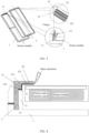
- FIG. 1 is a diagram of an assembly scenario of a screen module according to this application. As shown in FIG. 1 , first, the screen module is assembled into a metal housing 1. Then the screen module is clamped on the metal housing 1 through a border frame 2. In addition, the border frame 2 may also cover a gap formed between the screen module and the metal housing 1.
- FIG. 2 is a schematic diagram of a metal housing according to an embodiment of this application.
- the metal housing 1 may include a metal partition wall 11.
- One end of the metal partition wall 11 is connected to the metal housing 1, and the other end of the metal partition wall 11 extends in a direction away from the metal housing 1.
- An end surface 111 is formed at one end, away from the metal housing 1, of the metal partition wall 11.
- the metal partition wall 11 matches with the border frame 2 to fasten a screen module to the metal housing 1.
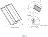
- FIG. 3 is a schematic sectional view of assembly of a screen module according to this application.
- FIG. 4 is a schematic diagram of a specific disposing manner of assembly of a screen module according to this application.
- a screen module is disposed on a side of a metal partition wall 11.
- a side of a border frame 2 is used as an example.
- the border frame 2 includes: a connection part 21, a first side edge 22, and a second side edge 23.
- the connection part 21 is disposed at one end, away from the metal housing 1, of the metal partition wall 11.
- the connection part 21 includes a first surface 211 facing the screen module and a junction surface 212 facing one side of the metal housing 1.
- the first side edge 22 is disposed on a side, facing the screen module, of the connection part 21.
- the first side edge 22 includes a second surface 221 facing the screen module.
- the second side edge 23 is disposed on a side, opposite to the screen module, of the metal partition wall 11.
- a continuous conductive layer is disposed on the junction surface 212, the first surface 211, and the second surface 221, and used to conduct static electricity.
- the junction surface 212 is connected to the end surface 111 and used to conduct the static electricity.
- the first side edge 22 is used to fasten the screen module, and the second side edge 23 is clamped to a groove formed by the metal partition wall 11 and the metal housing 1. It should be noted that, as shown in a dashed-line box in FIG. 4 , an electro-static sensitive area is disposed on a side of a side edge of the screen module, so that the static electricity easily enters along the side edge of the screen module.
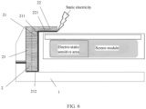
- FIG. 5 is a schematic sectional view of assembly of another screen module according to this application.
- FIG. 6 is a schematic diagram of a specific disposing manner of assembly of another screen module according to this application. A difference between a structure shown in FIG. 5 and
- FIG. 6 and a structure shown in FIG. 2 to FIG. 4 lies in that the metal housing 1 does not include the metal partition wall 11.
- the junction surface 212 is connected to the metal housing 1.
- FIG. 7 is a schematic diagram of an insulative electro-static discharge protection structure according to this application. As shown in FIG. 7 , a second surface 221, a first surface 211, and a side, facing a screen module, of a metal partition wall 11 are bonded to the screen module with solid adhesive.
- the solid adhesive has high compactness and is not easily broken down by static electricity. However, because insulation performance completely depends on a width of the adhesive, to achieve a good insulation effect, a width of a black edge of a screen may increase and affect appearance of the electronic device.
- an antenna of an electronic device is usually designed on a side of a side edge of the screen module. Enough wide space (for example, a clearance area) around the antenna of the electronic device is to be provided, without shielding or interference, to enable radiation intensity of signals at 360° in all directions at a cross section of the antenna to be the same, achieving a best communication effect.
- FIG. 8 is a schematic diagram of a grounding electro-static discharge protection structure according to this application.
- a second side edge 23 includes a third surface 231 facing a side of a metal housing 1 and a fourth surface 232 facing a side of a screen module.
- a continuous conductive layer is disposed on a second surface 221, a first surface 211, a junction surface 212, and a fourth surface 232.
- Conductive adhesive is disposed between the third surface 231 and the metal housing 1, and the conductive layer is connected to the metal housing 1 with the conductive adhesive.
- the conductive adhesive When entering from a side edge of the screen module, charges of static electricity are conducted to the conductive adhesive along the conductive layers, then conducted to the metal housing 1 with the conductive adhesive, and finally discharged by grounding. Therefore, in a process of manufacturing the electro-static discharge protection structure, the conductive adhesive is dispensed at a bottom of a groove formed by the metal partition wall 11 and the metal housing 1.
- An existing manufacturing process does not guarantee uniformity and compactness of dispensing.
- an amount of the conductive adhesive may increase a width of a black edge of a screen. This affects competitiveness on appearance of a product.
- an antenna area is disposed on a side, opposite to the screen module, of a border frame 2
- an antenna is disposed away from a component that causes interference as much as possible, to prevent harmonic interference caused by the component to the antenna.
- the electro-static discharge protection structure shown in FIG. 8 because the antenna area is close to grounding positions of the conductive layer and the conductive adhesive, an RSE risk is easily caused by poor grounding, and antenna performance is affected.
- a discharge in a gap includes two metal electrodes. One electrode is fastened to an insulator, the other electrode is connected to a grounding apparatus through an auxiliary gap, and a specified gap distance is maintained between the two electrodes. When an instantaneous overvoltage strikes, the gap is broken down, and a part of overvoltage charges are introduced into the ground. This prevents a voltage on a protected device from rising.
- FIG. 9 is a schematic diagram of another grounding electro-static discharge protection structure according to this application. As shown in FIG. 9 , the structure discharges static electricity in a manner of discharge in a gap.
- a continuous conductive layer is disposed on a second surface 221, a first surface 211, a junction surface 212, and a fourth surface 232.
- a conductive layer disposed on the fourth surface 232 extends from one end, away from a metal housing 1, of the second side edge 23 to a middle position of the second side edge 23, and is equivalent to an electrode fastened to an insulator.
- a specified gap distance is maintained between the conductive layer on the fourth surface 232 and a metal partition wall 11 for discharge in a gap.
- the metal partition wall 11 and the metal housing 1 are connected and grounded to discharge the static electricity.
- the metal partition wall 11 is equivalent to an electrode connected to a grounding apparatus through an auxiliary gap.
- charges of the static electricity are conducted along the conductive layer to break down the gap, conducted to the metal housing 1 through the metal partition wall 11, and discharged by grounding.
- Secondary discharge means abnormal discharge on a machined surface due to intervention of a pitting corrosion product and the like. During this abnormal discharge, arc sparks are produced. Such secondary discharge in an electronic device may cause a problem of freezing or poor call quality of a mobile phone.
- An existing technology of mounting a conductive layer is not advanced when the conductive layer is disposed. Taking a conductive copper sheet as an example, in the electro-static discharge protection structure shown in FIG. 9 , the conductive layer on the fourth surface 232 extends from the one end, away from the metal housing 1, of the second side edge 23 to a middle position of the fourth surface 232. A specific gap is left between the conductive layer and the metal partition wall 11.
- the conductive layer is made of the conductive copper sheet, when the electro-static discharge protection structure is disposed in the electronic device, due to limitations of the mounting technology, the conductive copper sheet is not fastened at a middle position and easily curls. When curling, the conductive copper sheet may be in contact with the metal partition wall 11, resulting in the secondary discharge.
- this embodiment of this application illustrates the electro-static discharge protection structure.
- the electro-static discharge protection structure static electricity on a side edge of the screen module is effectively discharged, electro-static discharge protection is effectively provided for each side edge of the screen module, antenna performance is ensured, an RSE risk caused by poor grounding in the conventional technology is prevented, and an impact on antenna performance is prevented, and a risk of secondary discharge is further prevented.
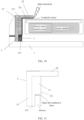
- FIG. 10 is a schematic diagram of an electro-static discharge protection structure according to an embodiment of this application.
- the electro-static discharge protection structure provided in this application includes a metal housing 1, a border frame 2, and a pressure-sensitive elastic component 3.
- One end of the pressure-sensitive elastic component 3 is connected to the metal housing 1, the other end of the pressure-sensitive elastic component 3 extends in a direction away from the metal housing 1, and a screen module is disposed on a side of the pressure-sensitive elastic component 3.
- the border frame 2 includes a connection part 21 and a first side edge 22.
- the connection part 21 is disposed at one end, away from the metal housing 1, of the pressure-sensitive elastic component 3.
- the connection part 21 includes a first surface 211 facing the screen module.
- the first side edge 22 is disposed on a side, facing the screen module, of the connection part 21.
- the first side edge 22 includes a second surface 221 facing the screen module.
- a conductive layer is disposed on a side, facing the pressure-sensitive elastic component 3, of the connection part 21, the one end of the pressure-sensitive elastic component 3 is connected to the conductive layer, the other end of the pressure-sensitive elastic component 3 is connected to the metal housing 1, and the conductive layer also continuously extends along the first surface 211 to the second surface 221.
- the pressure-sensitive elastic component 3 may be conductive only on at a high voltage. Therefore, a low voltage current may not be conducted to the metal partition wall 11 through the pressure-sensitive elastic component 3.
- the pressure-sensitive elastic component 3 includes: a pressure-sensitive device 31 and an elastic conductor 32.
- the pressure-sensitive device 31 is a device that can clamp a voltage when a circuit bears an overvoltage.
- the pressure-sensitive device 31 is not conductive when there is no static electricity, and is conductive when there is the static electricity.
- the elastic conductor 32 may absorb a gap tolerance. This improves reliability of overlapping, and reduces damage of a structural stress to the pressure-sensitive device 31.
- FIG. 11 is a schematic diagram of a disposing manner of a groove on a junction surface according to an embodiment of this application.
- the connection part 21 includes a junction surface 212 attached to the metal housing 1.
- a groove is disposed on the junction surface 212.
- the conductive layer is disposed at a bottom of the groove, the pressure-sensitive device 31 and the elastic conductor 32 are disposed in the groove.
- One end of the pressure-sensitive device 31 is connected to the conductive layer in the groove, the other end of the pressure-sensitive device 31 is connected to one end of the elastic conductor 32, and the other end of the elastic conductor 32 is connected to the metal housing 1.
- a window that is used to inject the conductive layer is disposed on the connection part 21, to facilitate the injection of the conductive layer and enable one end of the pressure-sensitive device 31 to be connected to the conductive layer.
- FIG. 12 is a schematic diagram of an electro-static discharge protection structure according to an embodiment of this application.
- a metal housing 1 includes a metal partition wall 11.
- One end of the metal partition wall 11 is connected to the metal housing 1, and the other end of the metal partition wall 11 extends in a direction away from the metal housing 1.
- a pressure-sensitive elastic component 3 is connected to one end, away from the metal housing 1, of the metal partition wall 11.
- the metal partition wall 11 is perpendicular to the metal housing 1.
- the metal partition wall 11 includes but is not limited to a solid cuboid or a hollow cuboid. When the metal partition wall 11 is the solid cuboid, a manufacturing process is simple, and the metal partition wall is easily poured and conductive entirely.
- connection part 21, the pressure-sensitive elastic component 3, and the metal partition wall 11 are disposed on a same plane. In actual arrangement, heights of the connection part 21, the pressure-sensitive elastic component 3, and the metal partition wall 11 may be adaptively set based on a setting requirement of an electronic device.
- first side edge 22 and the second side edge 23 are perpendicularly disposed in an L-shape, and the connection part 21 is disposed at a corner of the L-shape.
- the first surface 211 and a side edge, facing a side of the screen module, of metal partition wall 11 are located on a same plane.
- the metal housing 1, the metal partition wall 11, the first surface 211, and the second surface 221 form space for accommodating the screen module.
- a side edge, opposite to the screen module, of the metal partition wall 11 and the metal housing 1 form a rectangular groove, and the rectangular groove is clamped to the second side edge 23.
- FIG. 13 is a schematic diagram of a disposing manner of a groove on a junction surface according to an embodiment of this application.
- an end surface 111 is formed at the one end, away from the metal housing 1, of the metal partition wall 11.
- the connection part 21 includes a junction surface 212 attached to the end surface 111.
- a groove is disposed on the junction surface 212.
- the conductive layer is disposed at a bottom of the groove.
- the pressure-sensitive device 31 and the elastic conductor 32 are disposed in the groove.
- the pressure-sensitive elastic component 3 may be disposed on a border frame 2.
- the static electricity enters from a side edge of a screen, the static electricity is directly conducted to the pressure-sensitive device 31 through the conductive layer, then conducted to the metal partition wall 11 through the elastic conductor 32, and then discharged through the metal housing 1 by grounding. In the disposing manner, the static electricity is directly conducted to the pressure-sensitive device 31, so that the pressure-sensitive device 31 has a better effect of clamping a voltage.
- a window that is used to inject the conductive layer is disposed on the connection part 21, to facilitate the injection of the conductive layer and enable one end of the pressure-sensitive device 31 to be connected to the conductive layer.
- the second side edge 23 further includes a third surface 231.
- the third surface 231 is disposed on a side, facing the metal housing 1, of the second side edge 23. There is a gap between the third surface 231 and the metal housing 1.
- the pressure-sensitive elastic component 3 is disposed between the connection part 21 and the metal partition wall 11, so that the pressure-sensitive elastic component 3 is not conductive when there is no static electricity, and is conductive when there is the static electricity, and the metal partition wall 11 plays a role in clamping. Therefore, the third surface 231 does not need to be closely attached to the metal housing 1, the border frame 2 and the metal housing 1 do not need to be fastened with adhesive.
- the metal partition wall 11 When the metal partition wall 11 performs clamping, the metal partition wall 11 is not conductive when there is no static electricity. This prevents an increase of a width of a black edge of a screen caused when fastening to the metal housing 1 with the conductive adhesive, and prevents a problem of an RSE risk possibly caused by poor grounding with the conductive adhesive and further affecting antenna performance.
- FIG. 14 is a schematic diagram of a disposing manner of another pressure-sensitive elastic component according to an embodiment of this application.
- FIG. 15 is a schematic diagram of a disposing manner of a groove on an end surface according to an embodiment of this application.
- a groove is disposed on the end surface 111.
- a conductive layer is disposed at a top of the groove.
- a pressure-sensitive device 31 and an elastic conductor 32 are disposed in the groove.
- One end of the pressure-sensitive device 31 is connected to a bottom of the groove, the other end of the pressure-sensitive device 31 is connected to one end of the elastic conductor 32, and the other end of the elastic conductor 32 is connected to the conductive layer.
- the pressure-sensitive elastic component 3 may be disposed on the metal partition wall 11. Because the metal housing 1, the metal partition wall 11, and the groove disposed on the end surface 111 may be integrally poured in an actual manufacturing process, this manner is simpler in the manufacturing process.
- a border frame 2 includes at least any one of the following materials: a metal material and an insulating material.
- the border frame 2 of the electronic device may be manufactured based on needs of different user groups.
- the electro-static discharge protection structure illustrated in this application may be applied to a variety of materials of the border frame.
- a metal border frame may improve overall texture of the electronic device, an insulation border frame may provide a better radio frequency radiation capability and reduce an impact on the antenna performance.
- the conductive layer is disposed in at least any one of the following manners: spraying, transferring, and electroplating.
- the conductive layer in the actual manufacturing process, may be disposed based on a shape and a material of the electronic device.
- the pressure-sensitive device 31 includes at least any one of the following materials: a transient diode and a pressure-sensitive resistor.
- the transient diode is a highperformance protection device in a form of a diode, with characteristics of fast response time, high transient power, a low leakage current, and a small breakdown voltage deviation.
- the pressure-sensitive resistor may perform effective high-voltage transient voltage suppression, so that costs of the device are effectively reduced and an overall design is optimized.
- the elastic conductor 32 includes at least any one of the following materials: conductive foam and silicone. In the implementation, a plurality of materials may be selected as materials of the elastic conductor.
- the conductive layer includes at least any one of the following materials: conductive silver paste, a conductive copper sheet, conductive graphite, and conductive fabric. In this way, based on specific disposing of the electro-static discharge protection structure, a plurality of materials may be selected as materials of the conductive layer.
- the metal housing 1 is configured to implement grounding. In this way, static electricity is discharged by grounding through the metal housing 1.
- an antenna area is disposed on a side, opposite to the screen module, of the border frame 2. Due to a demand for a signal strength, an antenna is usually disposed near the border frame 2. An antenna area is disposed near the border frame 2, so that better radio frequency radiation is provided.
- An embodiment of this application further provides an electronic device.
- the electronic device includes the electro-static discharge protection structure provided in the foregoing embodiments.
- the electronic device may include, for example, a mobile terminal, a tablet computer, a personal computer, a workstation device, a large screen device (for example, a smart screen and an intelligent television), a handheld game console, a home game console, a virtual reality device, an augmented reality device, a mixed reality device, an intelligent vehicle terminal, a self-driving vehicle, customer-premises equipment (customer-premises equipment, CPE), and the like.
- the pressure-sensitive elastic component 3 may be conductive only at a high voltage.
- a low voltage current may not be conducted to the metal partition wall 11 through the pressure-sensitive elastic component 3. This prevents an RSE risk caused by conventional poor grounding, and further prevents affecting of antenna performance.
- the static electricity enters a side edge of the screen module, because of a high voltage of the static electricity, the static electricity is conducted to the pressure-sensitive elastic component 3 through the conductive layer, conducted to the metal partition wall 11, and then conducted to the metal housing 1 through the metal partition wall 11, and thereby being discharged by grounding.
Landscapes
- Engineering & Computer Science (AREA)
- Signal Processing (AREA)
- Microelectronics & Electronic Packaging (AREA)
- Elimination Of Static Electricity (AREA)
- Shielding Devices Or Components To Electric Or Magnetic Fields (AREA)
Abstract
Description
- This application claims priority to
Chinese Patent Application No. 202110992317.8, filed with the China National Intellectual Property Administration on August 27, 2021 - This application relates to the field of electro-static discharge protection technologies, and in particular to an electro-static discharge protection structure and an electronic device.
- In an electronic device such as a mobile phone, there may be static electricity on a side edge of a screen module. Electro-static discharge may cause frequent freezing, automatic power-off, poor image quality and volume, unstable signal quality, and the like of the mobile phone. Therefore, the electro-static discharge (Electro-Static discharge, ESD) has become important content for quality control of an electronic product.
- An existing electro-static discharge protection strategy applied to the electronic device mainly includes insulation and grounding. When electro-static discharge protection is performed by insulation, a border frame is bonded to the screen module with solid adhesive. The solid adhesive has high compactness and is not easily broken down by the static electricity. Electro-static discharge protection is mainly performed by grounding in the following two ways. In a first way, an electro-static discharge protection structure is fastened to a metal housing of an electronic device with conductive adhesive, to discharge static electricity by grounding. In a second way, the electro-static discharge protection structure discharges static electricity to the metal housing in a manner of discharge in a gap.
- However, the following problems exist in the foregoing two ways. When the electro-static discharge protection is performed by insulation, because insulation performance completely depends on a width of the adhesive, to achieve a good insulation effect, a width of a black edge of a screen may increase and affect appearance of the electronic device. When the electro-static discharged protection is performed by grounding, in the first grounding manner, conductive adhesive is dispensed to ensure stability of the electro-static discharge protection structure. This increases the width of the black edge of the screen. In addition, this grounding manner may cause a risk of radiated spurious emission (Radiated Spurious Emission, RSE) to an antenna due to poor grounding, and affect antenna performance. In the second grounding manner, the discharge in a gap may cause a risk of secondary discharge.
- Embodiments of this application provide an electro-static discharge protection structure and an electronic device, to prevent, without affecting antenna performance, risks of RSE and secondary discharge caused by poor grounding.
- According to a first aspect, this application provides an electro-static discharge protection structure. One end of a pressure-sensitive elastic component is connected to a metal housing, the other end of the pressure-sensitive elastic component extends in a direction away from the metal housing, and a screen module is disposed on a side of the pressure-sensitive elastic component. A border frame includes a connection part and a first side edge. The connection part is disposed at one end, away from the metal housing, of the pressure-sensitive elastic component. The connection part includes a first surface facing the screen module. The first side edge is disposed on a side, facing the screen module, of the connection part. The first side edge includes a second surface facing the screen module. A conductive layer is disposed on a side, facing the pressure-sensitive elastic component, of the connection part, the one end of the pressure-sensitive elastic component is connected to the conductive layer, the other end of the pressure-sensitive elastic component is connected to the metal housing, and the conductive layer also continuously extends along the first surface to the second surface.
- According to the electro-static discharge protection structure provided in this application, when there is no static electricity, the pressure-sensitive elastic component may be conductive only at a high voltage. Therefore, a low voltage current may not be conducted to a metal partition wall through the pressure-sensitive elastic component. This prevents an RSE risk caused by conventional poor grounding, and further prevents affecting of antenna performance. When the static electricity enters a side edge of the screen module, because of a high voltage of the static electricity, the static electricity is conducted to the pressure-sensitive elastic component through the conductive layer, and then conducted to the metal housing, thereby being discharged by grounding. It should be noted that the pressure-sensitive elastic component includes a pressure-sensitive device and an elastic conductor. The pressure-sensitive device is a device that can clamp a voltage when a circuit bears an overvoltage. The pressure-sensitive device is not conductive when there is no static electricity, and is conductive when there is the static electricity. Therefore, after the static electricity is conducted, a clamping voltage is extremely small, so that a peak current caused by secondary discharge is reduced, and a risk of the secondary discharge is prevented. The elastic conductor may absorb a gap tolerance. This improves reliability of overlapping, and reduces damage of a structural stress to the pressure-sensitive device.
- In an implementation, the metal housing includes a metal partition wall. One end of the metal partition wall is connected to the metal housing, the other end of the metal partition wall extends in the direction away from the metal housing, and the pressure-sensitive elastic component is connected to one end, away from the metal housing, of the metal partition wall. A height of the metal partition wall may be arbitrarily set, and may be clamped to the border frame, to fasten the border frame.
- In an implementation, the metal housing and the metal partition wall are integrally formed. In this way, in a process of manufacturing an electronic device, the metal housing and the metal partition wall may be integrally poured, to simplify a manufacturing process is simple. In addition, the metal housing and the metal partition wall are integrally poured and tightly connected. Therefore, when the static electricity is conducted, the static electricity is directly conducted to the metal housing through the metal partition wall, and discharged by grounding, so that a grounding effect is good. In an implementation, the border frame further includes a second side edge. The second side edge is disposed on a side, opposite to the screen module, of the metal partition wall. One end of the second side edge is connected to the connection part, and the other end of the second side edge extends in a direction close to the metal housing. The second side edge may be configured to be clamped to the metal partition wall.
- In an implementation, the connection part includes a junction surface attached to the metal housing. A groove is disposed on the junction surface, and the conductive layer is disposed at a bottom of the groove. The pressure-sensitive device and the elastic conductor are disposed in the groove. One end of the pressure-sensitive device is connected to the conductive layer in the groove, the other end of the pressure-sensitive device is connected to one end of the elastic conductor, and the other end of the elastic conductor is connected to the metal housing. In the implementation, the pressure-sensitive elastic component may be disposed on the border frame. When the static electricity enters from the side edge of the screen, the static electricity is conducted to the pressure-sensitive device through the conductive layer, then conducted to the metal housing through the elastic conductor, and discharged by grounding. In the disposing manner, no metal partition wall is disposed, the elastic conductor is directly connected to the metal housing, the pressure-sensitive elastic component may be fastened in a gap formed by the second side edge, the connection part, and the screen module. In the disposing manner, the static electricity is directly conducted to the pressure-sensitive device, so that the pressure-sensitive device has a better effect of clamping the voltage.
- In an implementation, an end surface is formed at the one end, away from the metal housing, of the metal partition wall. The connection part includes a junction surface attached to the end surface. A groove is disposed on the junction surface. The conductive layer is disposed at a bottom of the groove. The pressure-sensitive device and the elastic conductor are disposed in the groove. One end of the pressure-sensitive device is connected to the conductive layer in the groove, the other end of the pressure-sensitive device is connected to one end of the elastic conductor, and the other end of the elastic conductor is connected to the end surface. In the disposing manner, because the metal partition wall is disposed in this manner, and the metal partition wall may be clamped to the second side edge to fasten the border frame, the elastic conductor is directly connected to an end surface of the metal partition wall. In the disposing manner, the static electricity is directly conducted to the pressure-sensitive device, so that the pressure-sensitive device has a better effect of clamping the voltage.
- In an implementation, an end surface is formed at the one end, away from the metal housing, of the metal partition wall. The connection part includes the junction surface attached to the end surface. A groove is disposed on the end surface. The conductive layer is disposed at a top of the groove. The pressure-sensitive device and the elastic conductor are disposed in the groove. One end of the pressure-sensitive device is connected to a bottom of the groove, the other end of the pressure-sensitive device is connected to one end of the elastic conductor, and the other end of the elastic conductor is connected to the conductive layer. In the implementation, the pressure-sensitive elastic component may be disposed on the metal partition wall. Because the metal housing, the metal partition wall, and the groove disposed on the metal partition wall may be integrally poured in an actual manufacturing process, this manner is simpler in the manufacturing process.
- In an implementation, the border frame includes at least any one of the following materials: a metal material and an insulating material. In the manufacturing process, the border frame of the electronic device may be manufactured based on needs of different user groups. The electro-static discharge protection structure illustrated in this application may be applied to a variety of materials of the border frame. A metal border frame may improve overall texture of the electronic device, an insulation border frame may provide a better radio frequency radiation capability and reduce an impact on the antenna performance.
- In an implementation, the conductive layer is disposed in at least any one of the following manners: spraying, transferring, and electroplating. In the implementation, in the actual manufacturing process, the conductive layer may be disposed based on a shape and a material of the electronic device.
- In an implementation, the pressure-sensitive device includes at least any one of the following materials: a transient diode and a pressure-sensitive resistor. The transient diode is a highperformance protection device in a form of a diode, with characteristics of fast response time, high transient power, a low leakage current, and a small breakdown voltage deviation. The pressure-sensitive resistor may perform effective high-voltage transient voltage suppression, so that costs of the device are effectively reduced and an overall design is optimized.
- In an implementation, the elastic conductor includes at least any one of the following materials: conductive foam and silicone. In the implementation, a plurality of materials may be selected as materials of the elastic conductor.
- In an implementation, the conductive layer includes at least any one of the following materials: conductive silver paste, a conductive copper sheet, conductive graphite, and conductive fabric. In this way, based on specific disposing of the electro-static discharge protection structure, a plurality of materials may be selected as materials of the conductive layer.
- In an implementation, the second side edge further includes a third surface. The third surface is disposed on a side, facing the metal housing, of the second side edge. There is a gap between the third surface and the metal housing. In the implementation, the pressure-sensitive elastic component is disposed between the connection part and the metal partition wall, so that the pressure-sensitive elastic component is not conductive when there is no static electricity, and is conductive when there is the static electricity, and the metal partition wall plays a role in clamping. Therefore, the third surface does not need to be closely attached to the metal housing, and the border frame and the metal housing do not need to be fastened with adhesive. When the metal partition wall performing clamping, the metal partition wall is not conductive when there is no static electricity. This prevents an increase of a width of a black edge of a screen caused when the metal partition wall fastened to the metal housing with conductive adhesive, and prevents a problem of an RSE risk possibly caused by poor grounding with the conductive adhesive and further prevents affecting of antenna performance.
- In an implementation, an antenna area is disposed on a side, opposite to the screen module, of the border frame. Due to a demand for a signal strength, an antenna is usually disposed near the border frame. An antenna area is disposed near the border frame, so that better radio frequency radiation is provided.
- According to a second aspect, this application further provides an electronic device. The electronic device includes the electro-static discharge protection structure according to the first aspect and any one of the implementations in the first aspect.
- According to the electronic device provided in this application, when there is no static electricity, the pressure-sensitive elastic component may be conductive only at a high voltage, Therefore, a low voltage current may not be conducted to the metal partition wall through the pressure-sensitive elastic component. This prevents an RSE risk caused by conventional poor grounding, and further prevents affecting of antenna performance. When the static electricity enters a side edge of the screen module, because of a high voltage of the static electricity, the static electricity is conducted to the pressure-sensitive elastic component through the conductive layer, and then conducted to the metal housing, thereby being discharged by grounding.
-
-
FIG. 1 is a diagram of an assembly scenario of a screen module according to this application; -
FIG. 2 is a schematic diagram of a metal housing according to an embodiment of this application; -
FIG. 3 is a schematic sectional view of assembly of a screen module according to this application; -
FIG. 4 is a schematic diagram of a specific disposing manner of assembly of a screen module according to this application; -
FIG. 5 is a schematic sectional view of assembly of another screen module according to this application; -
FIG. 6 is a schematic diagram of a specific disposing manner of assembly of a screen module according to this application; -
FIG. 7 is a schematic diagram of an insulative electro-static discharge protection structure according to this application; -
FIG. 8 is a schematic diagram of a grounding electro-static discharge protection structure according to this application; -
FIG. 9 is a schematic diagram of another grounding electro-static discharge protection structure according to this application; -
FIG. 10 is a schematic diagram of an electro-static discharge protection structure according to an embodiment of this application; -
FIG. 11 is a schematic diagram of a disposing manner of a groove on a junction surface according to an embodiment of this application; -
FIG. 12 is a schematic diagram of an electro-static discharge protection structure according to an embodiment of this application; -
FIG. 13 is a schematic diagram of a disposing manner of a groove on a junction surface according to an embodiment of this application; -
FIG. 14 is a schematic diagram of a disposing manner of another pressure-sensitive elastic component according to an embodiment of this application; and -
FIG. 15 is a schematic diagram of a disposing manner of a groove on an end surface according to an embodiment of this application. - In an electronic device such as a mobile phone, there may be static electricity on a side edge of a screen module. An electro-static sensitive area is disposed on one side edge of the screen module, and the static electricity easily enters along the side edge of the screen module and is transmitted to other areas through a conductive layer. Static electricity has characteristics of long-time accumulation, a high voltage, a low battery level, a small current, and a short action event. Electro-static discharge may cause frequent freezing, automatic power-off, poor image quality and volume, unstable signal quality, and the like of the mobile phone. Therefore, ESD has become important content for quality control of an electronic product. ESD certification is to be performed in a process of launching an electronic device on the market. Therefore, electro-static discharge protection is important to the electronic device. An existing strategy to resolve the static electricity is insulation or grounding.
- When electro-static discharge protection is performed by insulation, a border frame is bonded to a metal housing with solid adhesive. The solid adhesive has high compactness and is not easily broken down by the static electricity.
-
FIG. 1 is a diagram of an assembly scenario of a screen module according to this application. As shown inFIG. 1 , first, the screen module is assembled into ametal housing 1. Then the screen module is clamped on themetal housing 1 through aborder frame 2. In addition, theborder frame 2 may also cover a gap formed between the screen module and themetal housing 1. -
FIG. 2 is a schematic diagram of a metal housing according to an embodiment of this application. As shown inFIG. 2 , themetal housing 1 may include ametal partition wall 11. One end of themetal partition wall 11 is connected to themetal housing 1, and the other end of themetal partition wall 11 extends in a direction away from themetal housing 1. Anend surface 111 is formed at one end, away from themetal housing 1, of themetal partition wall 11. Themetal partition wall 11 matches with theborder frame 2 to fasten a screen module to themetal housing 1. -
FIG. 3 is a schematic sectional view of assembly of a screen module according to this application.FIG. 4 is a schematic diagram of a specific disposing manner of assembly of a screen module according to this application. As shown inFIG. 3 and FIG. 4 , it may be learned, when split along dotted lines inFIG. 3 , a screen module is disposed on a side of ametal partition wall 11. A side of aborder frame 2 is used as an example. Theborder frame 2 includes: aconnection part 21, afirst side edge 22, and asecond side edge 23. Theconnection part 21 is disposed at one end, away from themetal housing 1, of themetal partition wall 11. Theconnection part 21 includes afirst surface 211 facing the screen module and ajunction surface 212 facing one side of themetal housing 1. Thefirst side edge 22 is disposed on a side, facing the screen module, of theconnection part 21. Thefirst side edge 22 includes asecond surface 221 facing the screen module. Thesecond side edge 23 is disposed on a side, opposite to the screen module, of themetal partition wall 11. A continuous conductive layer is disposed on thejunction surface 212, thefirst surface 211, and thesecond surface 221, and used to conduct static electricity. Thejunction surface 212 is connected to theend surface 111 and used to conduct the static electricity. Thefirst side edge 22 is used to fasten the screen module, and thesecond side edge 23 is clamped to a groove formed by themetal partition wall 11 and themetal housing 1. It should be noted that, as shown in a dashed-line box inFIG. 4 , an electro-static sensitive area is disposed on a side of a side edge of the screen module, so that the static electricity easily enters along the side edge of the screen module. -
FIG. 5 is a schematic sectional view of assembly of another screen module according to this application.FIG. 6 is a schematic diagram of a specific disposing manner of assembly of another screen module according to this application. A difference between a structure shown inFIG. 5 and -
FIG. 6 and a structure shown inFIG. 2 to FIG. 4 lies in that themetal housing 1 does not include themetal partition wall 11. Thejunction surface 212 is connected to themetal housing 1.FIG. 7 is a schematic diagram of an insulative electro-static discharge protection structure according to this application. As shown inFIG. 7 , asecond surface 221, afirst surface 211, and a side, facing a screen module, of ametal partition wall 11 are bonded to the screen module with solid adhesive. The solid adhesive has high compactness and is not easily broken down by static electricity. However, because insulation performance completely depends on a width of the adhesive, to achieve a good insulation effect, a width of a black edge of a screen may increase and affect appearance of the electronic device. - At present, an antenna of an electronic device is usually designed on a side of a side edge of the screen module. Enough wide space (for example, a clearance area) around the antenna of the electronic device is to be provided, without shielding or interference, to enable radiation intensity of signals at 360° in all directions at a cross section of the antenna to be the same, achieving a best communication effect.
-
FIG. 8 is a schematic diagram of a grounding electro-static discharge protection structure according to this application. As shown inFIG. 8 , asecond side edge 23 includes athird surface 231 facing a side of ametal housing 1 and afourth surface 232 facing a side of a screen module. A continuous conductive layer is disposed on asecond surface 221, afirst surface 211, ajunction surface 212, and afourth surface 232. Conductive adhesive is disposed between thethird surface 231 and themetal housing 1, and the conductive layer is connected to themetal housing 1 with the conductive adhesive. When entering from a side edge of the screen module, charges of static electricity are conducted to the conductive adhesive along the conductive layers, then conducted to themetal housing 1 with the conductive adhesive, and finally discharged by grounding. Therefore, in a process of manufacturing the electro-static discharge protection structure, the conductive adhesive is dispensed at a bottom of a groove formed by themetal partition wall 11 and themetal housing 1. An existing manufacturing process does not guarantee uniformity and compactness of dispensing. To ensure performance and a degree of adhesion of the conductive adhesive, when the adhesive is dispensed in a groove with a specific depth, an amount of the conductive adhesive may increase a width of a black edge of a screen. This affects competitiveness on appearance of a product. In addition, because an antenna area is disposed on a side, opposite to the screen module, of aborder frame 2, an antenna is disposed away from a component that causes interference as much as possible, to prevent harmonic interference caused by the component to the antenna. According to the electro-static discharge protection structure shown inFIG. 8 , because the antenna area is close to grounding positions of the conductive layer and the conductive adhesive, an RSE risk is easily caused by poor grounding, and antenna performance is affected. - A discharge in a gap includes two metal electrodes. One electrode is fastened to an insulator, the other electrode is connected to a grounding apparatus through an auxiliary gap, and a specified gap distance is maintained between the two electrodes. When an instantaneous overvoltage strikes, the gap is broken down, and a part of overvoltage charges are introduced into the ground. This prevents a voltage on a protected device from rising.
-
FIG. 9 is a schematic diagram of another grounding electro-static discharge protection structure according to this application. As shown inFIG. 9 , the structure discharges static electricity in a manner of discharge in a gap. A continuous conductive layer is disposed on asecond surface 221, afirst surface 211, ajunction surface 212, and afourth surface 232. A conductive layer disposed on thefourth surface 232 extends from one end, away from ametal housing 1, of thesecond side edge 23 to a middle position of thesecond side edge 23, and is equivalent to an electrode fastened to an insulator. A specified gap distance is maintained between the conductive layer on thefourth surface 232 and ametal partition wall 11 for discharge in a gap. Themetal partition wall 11 and themetal housing 1 are connected and grounded to discharge the static electricity. Themetal partition wall 11 is equivalent to an electrode connected to a grounding apparatus through an auxiliary gap. When the static electricity enters from a side edge of a screen module, charges of the static electricity are conducted along the conductive layer to break down the gap, conducted to themetal housing 1 through themetal partition wall 11, and discharged by grounding. - Secondary discharge means abnormal discharge on a machined surface due to intervention of a pitting corrosion product and the like. During this abnormal discharge, arc sparks are produced. Such secondary discharge in an electronic device may cause a problem of freezing or poor call quality of a mobile phone. An existing technology of mounting a conductive layer is not advanced when the conductive layer is disposed. Taking a conductive copper sheet as an example, in the electro-static discharge protection structure shown in
FIG. 9 , the conductive layer on thefourth surface 232 extends from the one end, away from themetal housing 1, of thesecond side edge 23 to a middle position of thefourth surface 232. A specific gap is left between the conductive layer and themetal partition wall 11. If the conductive layer is made of the conductive copper sheet, when the electro-static discharge protection structure is disposed in the electronic device, due to limitations of the mounting technology, the conductive copper sheet is not fastened at a middle position and easily curls. When curling, the conductive copper sheet may be in contact with themetal partition wall 11, resulting in the secondary discharge. - To solve the problems in a conventional technology, this embodiment of this application illustrates the electro-static discharge protection structure. According to the electro-static discharge protection structure, static electricity on a side edge of the screen module is effectively discharged, electro-static discharge protection is effectively provided for each side edge of the screen module, antenna performance is ensured, an RSE risk caused by poor grounding in the conventional technology is prevented, and an impact on antenna performance is prevented, and a risk of secondary discharge is further prevented.
-
FIG. 10 is a schematic diagram of an electro-static discharge protection structure according to an embodiment of this application. As shown inFIG. 10 , the electro-static discharge protection structure provided in this application includes ametal housing 1, aborder frame 2, and a pressure-sensitiveelastic component 3. One end of the pressure-sensitiveelastic component 3 is connected to themetal housing 1, the other end of the pressure-sensitiveelastic component 3 extends in a direction away from themetal housing 1, and a screen module is disposed on a side of the pressure-sensitiveelastic component 3. Theborder frame 2 includes aconnection part 21 and afirst side edge 22. Theconnection part 21 is disposed at one end, away from themetal housing 1, of the pressure-sensitiveelastic component 3. Theconnection part 21 includes afirst surface 211 facing the screen module. Thefirst side edge 22 is disposed on a side, facing the screen module, of theconnection part 21. Thefirst side edge 22 includes asecond surface 221 facing the screen module. A conductive layer is disposed on a side, facing the pressure-sensitiveelastic component 3, of theconnection part 21, the one end of the pressure-sensitiveelastic component 3 is connected to the conductive layer, the other end of the pressure-sensitiveelastic component 3 is connected to themetal housing 1, and the conductive layer also continuously extends along thefirst surface 211 to thesecond surface 221. When there is no static electricity, the pressure-sensitiveelastic component 3 may be conductive only on at a high voltage. Therefore, a low voltage current may not be conducted to themetal partition wall 11 through the pressure-sensitiveelastic component 3. This prevents an impact of an RSE risk caused by conventional poor grounding, on antenna performance. When the static electricity enters a side edge of the screen module, because of a high voltage of the static electricity, the static electricity is conducted to the pressure-sensitiveelastic component 3 through the conductive layer, and then conducted to themetal housing 1, thereby being discharged by grounding. It should be noted that the pressure-sensitiveelastic component 3 includes: a pressure-sensitive device 31 and anelastic conductor 32. The pressure-sensitive device 31 is a device that can clamp a voltage when a circuit bears an overvoltage. The pressure-sensitive device 31 is not conductive when there is no static electricity, and is conductive when there is the static electricity. Therefore, after the static electricity is conducted, a clamping voltage is extremely small, so that a peak current caused by secondary discharge is reduced, and a risk of secondary discharge is prevented. Theelastic conductor 32 may absorb a gap tolerance. This improves reliability of overlapping, and reduces damage of a structural stress to the pressure-sensitive device 31. -
FIG. 11 is a schematic diagram of a disposing manner of a groove on a junction surface according to an embodiment of this application. As shown inFIG. 10 and FIG. 11 , theconnection part 21 includes ajunction surface 212 attached to themetal housing 1. A groove is disposed on thejunction surface 212. The conductive layer is disposed at a bottom of the groove, the pressure-sensitive device 31 and theelastic conductor 32 are disposed in the groove. One end of the pressure-sensitive device 31 is connected to the conductive layer in the groove, the other end of the pressure-sensitive device 31 is connected to one end of theelastic conductor 32, and the other end of theelastic conductor 32 is connected to themetal housing 1. It should be noted that, as shown in a dashed-line box at the bottom of the groove inFIG. 11 , a window that is used to inject the conductive layer is disposed on theconnection part 21, to facilitate the injection of the conductive layer and enable one end of the pressure-sensitive device 31 to be connected to the conductive layer. -
FIG. 12 is a schematic diagram of an electro-static discharge protection structure according to an embodiment of this application. As shown inFIG. 12 , in an implementation, ametal housing 1 includes ametal partition wall 11. One end of themetal partition wall 11 is connected to themetal housing 1, and the other end of themetal partition wall 11 extends in a direction away from themetal housing 1. A pressure-sensitiveelastic component 3 is connected to one end, away from themetal housing 1, of themetal partition wall 11. Themetal partition wall 11 is perpendicular to themetal housing 1. Themetal partition wall 11 includes but is not limited to a solid cuboid or a hollow cuboid. When themetal partition wall 11 is the solid cuboid, a manufacturing process is simple, and the metal partition wall is easily poured and conductive entirely. When themetal partition wall 11 is the hollow cuboid, some of materials are reduced in a manufacturing process, and this facilitates heat dissipation of the screen module. Theconnection part 21, the pressure-sensitiveelastic component 3, and themetal partition wall 11 are disposed on a same plane. In actual arrangement, heights of theconnection part 21, the pressure-sensitiveelastic component 3, and themetal partition wall 11 may be adaptively set based on a setting requirement of an electronic device. - In an implementation, the
first side edge 22 and thesecond side edge 23 are perpendicularly disposed in an L-shape, and theconnection part 21 is disposed at a corner of the L-shape. Thefirst surface 211 and a side edge, facing a side of the screen module, ofmetal partition wall 11 are located on a same plane. Themetal housing 1, themetal partition wall 11, thefirst surface 211, and thesecond surface 221 form space for accommodating the screen module. A side edge, opposite to the screen module, of themetal partition wall 11 and themetal housing 1 form a rectangular groove, and the rectangular groove is clamped to thesecond side edge 23. -
FIG. 13 is a schematic diagram of a disposing manner of a groove on a junction surface according to an embodiment of this application. As shown inFIG. 12 and FIG. 13 , in an implementation, anend surface 111 is formed at the one end, away from themetal housing 1, of themetal partition wall 11. Theconnection part 21 includes ajunction surface 212 attached to theend surface 111. A groove is disposed on thejunction surface 212. The conductive layer is disposed at a bottom of the groove. The pressure-sensitive device 31 and theelastic conductor 32 are disposed in the groove. One end of the pressure-sensitive device 31 is connected to the conductive layer in the groove, the other end of the pressure-sensitive device 31 is connected to one end of theelastic conductor 32, and the other end of theelastic conductor 32 is connected to theend surface 111. In the implementation, the pressure-sensitiveelastic component 3 may be disposed on aborder frame 2. When the static electricity enters from a side edge of a screen, the static electricity is directly conducted to the pressure-sensitive device 31 through the conductive layer, then conducted to themetal partition wall 11 through theelastic conductor 32, and then discharged through themetal housing 1 by grounding. In the disposing manner, the static electricity is directly conducted to the pressure-sensitive device 31, so that the pressure-sensitive device 31 has a better effect of clamping a voltage. It should be noted that, as shown in a dashed-line box at the bottom of the groove inFIG. 13 , a window that is used to inject the conductive layer is disposed on theconnection part 21, to facilitate the injection of the conductive layer and enable one end of the pressure-sensitive device 31 to be connected to the conductive layer. - In an implementation, the
second side edge 23 further includes athird surface 231. Thethird surface 231 is disposed on a side, facing themetal housing 1, of thesecond side edge 23. There is a gap between thethird surface 231 and themetal housing 1. In the implementation, the pressure-sensitiveelastic component 3 is disposed between theconnection part 21 and themetal partition wall 11, so that the pressure-sensitiveelastic component 3 is not conductive when there is no static electricity, and is conductive when there is the static electricity, and themetal partition wall 11 plays a role in clamping. Therefore, thethird surface 231 does not need to be closely attached to themetal housing 1, theborder frame 2 and themetal housing 1 do not need to be fastened with adhesive. When themetal partition wall 11 performs clamping, themetal partition wall 11 is not conductive when there is no static electricity. This prevents an increase of a width of a black edge of a screen caused when fastening to themetal housing 1 with the conductive adhesive, and prevents a problem of an RSE risk possibly caused by poor grounding with the conductive adhesive and further affecting antenna performance. -
FIG. 14 is a schematic diagram of a disposing manner of another pressure-sensitive elastic component according to an embodiment of this application.FIG. 15 is a schematic diagram of a disposing manner of a groove on an end surface according to an embodiment of this application. As shown inFIG. 14 and FIG. 15 , in an implementation, a groove is disposed on theend surface 111. A conductive layer is disposed at a top of the groove. A pressure-sensitive device 31 and anelastic conductor 32 are disposed in the groove. One end of the pressure-sensitive device 31 is connected to a bottom of the groove, the other end of the pressure-sensitive device 31 is connected to one end of theelastic conductor 32, and the other end of theelastic conductor 32 is connected to the conductive layer. In the implementation, the pressure-sensitiveelastic component 3 may be disposed on themetal partition wall 11. Because themetal housing 1, themetal partition wall 11, and the groove disposed on theend surface 111 may be integrally poured in an actual manufacturing process, this manner is simpler in the manufacturing process. - In an implementation, a
border frame 2 includes at least any one of the following materials: a metal material and an insulating material. In a manufacturing process, theborder frame 2 of the electronic device may be manufactured based on needs of different user groups. The electro-static discharge protection structure illustrated in this application may be applied to a variety of materials of the border frame. A metal border frame may improve overall texture of the electronic device, an insulation border frame may provide a better radio frequency radiation capability and reduce an impact on the antenna performance. - In an implementation, the conductive layer is disposed in at least any one of the following manners: spraying, transferring, and electroplating. In the implementation, in the actual manufacturing process, the conductive layer may be disposed based on a shape and a material of the electronic device.
- In an implementation, the pressure-
sensitive device 31 includes at least any one of the following materials: a transient diode and a pressure-sensitive resistor. The transient diode is a highperformance protection device in a form of a diode, with characteristics of fast response time, high transient power, a low leakage current, and a small breakdown voltage deviation. The pressure-sensitive resistor may perform effective high-voltage transient voltage suppression, so that costs of the device are effectively reduced and an overall design is optimized. - In an implementation, the
elastic conductor 32 includes at least any one of the following materials: conductive foam and silicone. In the implementation, a plurality of materials may be selected as materials of the elastic conductor. - In an implementation, the conductive layer includes at least any one of the following materials: conductive silver paste, a conductive copper sheet, conductive graphite, and conductive fabric. In this way, based on specific disposing of the electro-static discharge protection structure, a plurality of materials may be selected as materials of the conductive layer.
- In an implementation, the
metal housing 1 is configured to implement grounding. In this way, static electricity is discharged by grounding through themetal housing 1. - In an implementation, an antenna area is disposed on a side, opposite to the screen module, of the
border frame 2. Due to a demand for a signal strength, an antenna is usually disposed near theborder frame 2. An antenna area is disposed near theborder frame 2, so that better radio frequency radiation is provided. - An embodiment of this application further provides an electronic device. The electronic device includes the electro-static discharge protection structure provided in the foregoing embodiments. The electronic device may include, for example, a mobile terminal, a tablet computer, a personal computer, a workstation device, a large screen device (for example, a smart screen and an intelligent television), a handheld game console, a home game console, a virtual reality device, an augmented reality device, a mixed reality device, an intelligent vehicle terminal, a self-driving vehicle, customer-premises equipment (customer-premises equipment, CPE), and the like. According to the electronic device, when there is no static electricity, the pressure-sensitive
elastic component 3 may be conductive only at a high voltage. Therefore, a low voltage current may not be conducted to themetal partition wall 11 through the pressure-sensitiveelastic component 3. This prevents an RSE risk caused by conventional poor grounding, and further prevents affecting of antenna performance. When the static electricity enters a side edge of the screen module, because of a high voltage of the static electricity, the static electricity is conducted to the pressure-sensitiveelastic component 3 through the conductive layer, conducted to themetal partition wall 11, and then conducted to themetal housing 1 through themetal partition wall 11, and thereby being discharged by grounding.
Claims (15)
- An electro-static discharge protection structure, comprising: a metal housing (1), a border frame (2), and a pressure-sensitive elastic component (3), wherein the pressure-sensitive elastic component (3) comprises: a pressure-sensitive device (31) and an elastic conductor (32);one end of the pressure-sensitive elastic component (3) is connected to the metal housing (1), the other end of the pressure-sensitive elastic component (3) extends in a direction away from the metal housing (1), and a screen module is disposed on a side of the pressure-sensitive elastic component (3);the border frame (2) comprises a connection part (21) and a first side edge (22);the connection part (21) is disposed at one end, away from the metal housing (1), of the pressure-sensitive elastic component (3), and the connection part (21) comprises a first surface (211) facing the screen module;the first side edge (22) is disposed on a side, facing the screen module, of the connection part (21), and the first side edge (22) comprises a second surface (221) facing the screen module; anda conductive layer is disposed on a side, facing the pressure-sensitive elastic component (3), of the connection part (21), the one end of the pressure-sensitive elastic component (3) is connected to the conductive layer, the other end of the pressure-sensitive elastic component (3) is connected to the metal housing (1), and the conductive layer also continuously extends along the first surface (211) to the second surface (221).
- The electro-static discharge protection structure according to claim 1, wherein the metal housing (1) comprises a metal partition wall (11); and
one end of the metal partition wall (11) is connected to the metal housing (1), and the other end of the metal partition wall (11) extends in the direction away from the metal housing (1), and the pressure-sensitive elastic component (3) is connected to one end, away from the metal housing (1), of the metal partition wall (11). - The electro-static discharge protection structure according to claim 2, wherein the metal housing (1) and the metal partition wall (11) are integrally formed.
- The electro-static discharge protection structure according to claim 3, wherein the border frame (2) further comprises a second side edge (23);the second side edge (23) is disposed on a side, opposite to the screen module, of the metal partition wall (11); andone end of the second side edge (23) is connected to the connection part (21), and the other end of the second side edge (23) extends in a direction close to the metal housing (1).
- The electro-static discharge protection structure according to claim 1, wherein the connection part (21) comprises a junction surface (212) attached to the metal housing (1); and a groove is disposed on the junction surface (212), the conductive layer is disposed at a bottom of the groove, the pressure-sensitive device (31) and the elastic conductor (32) are disposed in the groove, one end of the pressure-sensitive device (31) is connected to the conductive layer in the groove, the other end of the pressure-sensitive device (31) is connected to one end of the elastic conductor (32), and the other end of the elastic conductor (32) is connected to the metal housing (1).
- The electro-static discharge protection structure according to claim 4, wherein an end surface (111) is formed at the one end, away from the metal housing (1), of the metal partition wall (11), the connection part (21) comprises a junction surface (212) attached to the end surface (111), a groove is disposed on the junction surface (212), and the conductive layer is disposed at a bottom of the groove; and the pressure-sensitive device (31) and the elastic conductor (32) are disposed in the groove, one end of the pressure-sensitive device (31) is connected to the conductive layer in the groove, the other end of the pressure-sensitive device (31) is connected to one end of the elastic conductor (32), and the other end of the elastic conductor (32) is connected to the end surface (111).
- The electro-static discharge protection structure according to claim 4, wherein an end surface (111) is formed at the one end, away from the metal housing (1), of the metal partition wall (11), the connection part (21) comprises a junction surface (212) attached to the end surface (111), a groove is disposed on the end surface (111), and the conductive layer is disposed at a top of the groove; and the pressure-sensitive device (31) and the elastic conductor (32) are disposed in the groove, one end of the pressure-sensitive device (31) is connected to a bottom of the groove, the other end of the pressure-sensitive device (31) is connected to one end of the elastic conductor (32), and the other end of the elastic conductor (32) is connected to the conductive layer.
- The electro-static discharge protection structure according to claim 1, wherein the border frame (2) comprises at least any one of the following materials: a metal material and an insulating material.
- The electro-static discharge protection structure according to claim 1, wherein the conductive layer is disposed in at least any one of the following manners: spraying, transferring, and electroplating.
- The electro-static discharge protection structure according to claim 1, wherein the pressure-sensitive device (31) comprises at least any one of the following materials: a transient diode and a pressure-sensitive resistor.
- The electro-static discharge protection structure according to claim 1, wherein the elastic conductor (32) comprises at least any one of the following materials: conductive foam and silicone.
- The electro-static discharge protection structure according to claim 1, wherein the conductive layer comprises at least any one of the following materials: conductive silver paste, a conductive copper sheet, conductive graphite, and conductive fabric.
- The electro-static discharge protection structure according to claim 4, wherein the second side edge (23) further comprises a third surface (231);the third surface (231) is disposed on a side, facing the metal housing (1), of the second side edge (23); andthere is a gap between the third surface (231) and the metal housing (1).
- The electro-static discharge protection structure according to claim 1, wherein an antenna area is disposed on a side, opposite to the screen module, of the border frame (2).
- An electronic device, comprising the electro-static discharge protection structure according to any one of claims 1 to 14.
Applications Claiming Priority (2)
| Application Number | Priority Date | Filing Date | Title |
|---|---|---|---|
| CN202110992317.8A CN113853053B (en) | 2021-08-27 | 2021-08-27 | Electrostatic protection structure and electronic equipment |
| PCT/CN2022/087626 WO2023024534A1 (en) | 2021-08-27 | 2022-04-19 | Electrostatic protection structure and electronic device |
Publications (3)
| Publication Number | Publication Date |
|---|---|
| EP4284121A1 true EP4284121A1 (en) | 2023-11-29 |
| EP4284121A4 EP4284121A4 (en) | 2024-12-04 |
| EP4284121B1 EP4284121B1 (en) | 2025-10-08 |
Family
ID=78976176
Family Applications (1)
| Application Number | Title | Priority Date | Filing Date |
|---|---|---|---|
| EP22859888.4A Active EP4284121B1 (en) | 2021-08-27 | 2022-04-19 | Electrostatic protection structure and electronic device |
Country Status (4)
| Country | Link |
|---|---|
| US (1) | US12543300B2 (en) |
| EP (1) | EP4284121B1 (en) |
| CN (1) | CN113853053B (en) |
| WO (1) | WO2023024534A1 (en) |
Cited By (1)
| Publication number | Priority date | Publication date | Assignee | Title |
|---|---|---|---|---|
| WO2026034777A1 (en) * | 2024-08-05 | 2026-02-12 | 삼성전자 주식회사 | Electronic device including electrostatic discharge path |
Families Citing this family (4)
| Publication number | Priority date | Publication date | Assignee | Title |
|---|---|---|---|---|
| CN113853053B (en) | 2021-08-27 | 2022-07-26 | 荣耀终端有限公司 | Electrostatic protection structure and electronic equipment |
| CN114286614A (en) * | 2021-12-30 | 2022-04-05 | 维沃移动通信有限公司 | Electronic device |
| CN119889162A (en) * | 2025-01-17 | 2025-04-25 | 维沃移动通信有限公司 | Electronic equipment |
| CN120343892B (en) * | 2025-06-19 | 2025-11-11 | 荣耀终端股份有限公司 | Electronic device components, protection components and electronic devices |
Family Cites Families (37)
| Publication number | Priority date | Publication date | Assignee | Title |
|---|---|---|---|---|
| US4925400A (en) * | 1988-09-30 | 1990-05-15 | Amp Incorporated | ESD protected electrical connector and ESD grounding clip therefor, and circuit panel connector assembly and method of assembling same |
| US6028761A (en) * | 1997-03-04 | 2000-02-22 | C-Technologies Llc | Apparatus and method for monitoring, controlling, displaying and dissipating an electrostatic charge |
| GB2389719B (en) * | 2002-06-13 | 2007-04-18 | Alan Abraham Deal | Mobile telephones and like devices |
| JP2005123001A (en) | 2003-10-16 | 2005-05-12 | Fuji Photo Film Co Ltd | Electrostatic damage prevention member and electrostatic damage prevention structure |
| US7248455B2 (en) * | 2003-10-31 | 2007-07-24 | International Business Machines Corporation | Method and apparatus for providing compressive connection with electrostatic discharge dissipative properties |
| JP2008065070A (en) * | 2006-09-07 | 2008-03-21 | Ricoh Co Ltd | Image forming apparatus and method |
| US8238087B2 (en) * | 2010-01-06 | 2012-08-07 | Apple Inc. | Display module |
| CN201248189Y (en) * | 2008-07-10 | 2009-05-27 | 深圳华为通信技术有限公司 | Metal casing floating ground equipment and veneer for elusion of floating ground voltage |
| CN201263150Y (en) * | 2008-09-18 | 2009-06-24 | 周雅洁 | Mobile phone antenna circuit for preventing electrostatic discharging |
| CN102111948A (en) * | 2009-12-23 | 2011-06-29 | 深圳富泰宏精密工业有限公司 | Shrapnel structure and electronic device applying same |
| CN202067055U (en) * | 2011-05-17 | 2011-12-07 | 京东方科技集团股份有限公司 | Anti-static liquid crystal display screen |
| CN202406151U (en) * | 2011-12-05 | 2012-08-29 | 惠州Tcl移动通信有限公司 | Mobile phone capable of reducing radiation stray |
| US9075567B2 (en) * | 2012-06-08 | 2015-07-07 | Apple Inc. | Electronic device display structures |
| WO2015140856A1 (en) * | 2014-03-18 | 2015-09-24 | パナソニックIpマネジメント株式会社 | Electronic apparatus |
| CN106161744B (en) | 2014-10-23 | 2019-06-14 | Lg电子株式会社 | Mobile terminal and control method thereof |
| DE102015108537B4 (en) | 2015-05-29 | 2019-07-04 | Infineon Technologies Dresden Gmbh | Semiconductor device with electrostatic discharge protection structure |
| KR101704644B1 (en) | 2016-02-24 | 2017-02-08 | 주식회사 아모텍 | Contactor with guide and mobile electronic apparatus with the same |
| KR101977270B1 (en) * | 2016-02-24 | 2019-05-10 | 주식회사 아모텍 | Contactor with guide and mobile electronic apparatus with the same |
| KR101738984B1 (en) | 2016-05-26 | 2017-05-24 | 주식회사 모다이노칩 | Contactor for preventing |
| WO2018047491A1 (en) * | 2016-09-06 | 2018-03-15 | ソニーセミコンダクタソリューションズ株式会社 | Electronic device, camera apparatus, and shield chassis |
| WO2018194103A1 (en) * | 2017-04-19 | 2018-10-25 | Agc株式会社 | Cover member and display device |
| CN207531214U (en) * | 2017-11-24 | 2018-06-22 | 维沃移动通信有限公司 | A kind of electronic equipment |
| CN108023978B (en) * | 2017-11-29 | 2019-10-18 | 维沃移动通信有限公司 | a terminal device |
| CN207664354U (en) | 2017-12-29 | 2018-07-27 | 华蓥市海通电子科技有限公司 | A kind of antistatic HDMI plugs |
| CN108391191A (en) * | 2018-01-30 | 2018-08-10 | 努比亚技术有限公司 | A kind of Headphone structure and mobile terminal |
| CN108615967B (en) * | 2018-04-26 | 2020-12-15 | Oppo广东移动通信有限公司 | Housing assembly, antenna assembly and electronic equipment |
| CN208413398U (en) * | 2018-05-14 | 2019-01-22 | 东莞市金丰包装材料有限公司 | A kind of static elimination device for tape rewinder |
| CN108769315A (en) * | 2018-05-30 | 2018-11-06 | 维沃移动通信有限公司 | A kind of mobile terminal and circuit control method |
| KR102474751B1 (en) * | 2018-07-20 | 2022-12-07 | 삼성전자주식회사 | Electronic device including structure for protecting display driver from static electricity |
| CN110233915B (en) * | 2019-05-21 | 2021-10-15 | 荣耀终端有限公司 | Electronic equipment |
| KR20210046879A (en) * | 2019-10-18 | 2021-04-29 | 삼성디스플레이 주식회사 | Display device |
| US11637919B2 (en) * | 2019-12-03 | 2023-04-25 | Apple Inc. | Handheld electronic device |
| CN212102676U (en) * | 2020-05-06 | 2020-12-08 | 东莞市安道光电材料制造有限公司 | Novel high-strength double-sided adhesive tape |
| CN112993606B (en) * | 2021-02-07 | 2023-01-10 | 维沃移动通信有限公司 | Electronic equipment and preparation method of elastic grounding assembly |
| JP7595393B2 (en) * | 2021-03-30 | 2024-12-06 | パナソニックオートモーティブシステムズ株式会社 | In-vehicle display device |
| CN213958451U (en) * | 2021-07-19 | 2021-08-13 | 荣耀终端有限公司 | a display device |
| CN113853053B (en) | 2021-08-27 | 2022-07-26 | 荣耀终端有限公司 | Electrostatic protection structure and electronic equipment |
-
2021
- 2021-08-27 CN CN202110992317.8A patent/CN113853053B/en active Active
-
2022
- 2022-04-19 EP EP22859888.4A patent/EP4284121B1/en active Active
- 2022-04-19 US US18/279,668 patent/US12543300B2/en active Active
- 2022-04-19 WO PCT/CN2022/087626 patent/WO2023024534A1/en not_active Ceased
Cited By (1)
| Publication number | Priority date | Publication date | Assignee | Title |
|---|---|---|---|---|
| WO2026034777A1 (en) * | 2024-08-05 | 2026-02-12 | 삼성전자 주식회사 | Electronic device including electrostatic discharge path |
Also Published As
| Publication number | Publication date |
|---|---|
| US12543300B2 (en) | 2026-02-03 |
| EP4284121B1 (en) | 2025-10-08 |
| CN113853053B (en) | 2022-07-26 |
| CN113853053A (en) | 2021-12-28 |
| EP4284121A4 (en) | 2024-12-04 |
| WO2023024534A1 (en) | 2023-03-02 |
| US20240314989A1 (en) | 2024-09-19 |
Similar Documents
| Publication | Publication Date | Title |
|---|---|---|
| EP4284121B1 (en) | Electrostatic protection structure and electronic device | |
| EP4351290A1 (en) | Electrostatic protection structure and electronic device | |
| US12088024B2 (en) | Antenna having high isolation and low cross-polarization level, base station, and terminal | |
| US20250358988A1 (en) | Electronic device | |
| KR20010086337A (en) | Lightning protection for an active antenna using patch/microstrip elements | |
| CN1277438C (en) | Mobile telephone set | |
| CN211062980U (en) | Connector male end assembly | |
| CN102548173B (en) | A kind of electrostatic charge protection method and mobile terminal | |
| CN202635004U (en) | Electromagnetic shielding structure applied to electronic equipment | |
| EP4730942A1 (en) | Shielding structure and electronic apparatus | |
| RU2729962C1 (en) | Antenna unit and electronic device | |
| WO2021000170A1 (en) | Full-screen electronic device and antenna thereof | |
| EP2808959B1 (en) | High voltage discharge protection device and radio frequency transmission apparatus using the same | |
| CN211062914U (en) | Female terminal assembly of connector | |
| CN217523043U (en) | Terminal device | |
| CN217282212U (en) | Mounting bracket | |
| CN218101955U (en) | Multichannel antenna feeder surge protector | |
| CN220234199U (en) | Power supply filtering lightning protection assembly and shelter | |
| CN119485883A (en) | Electrostatic protection device and electronic equipment | |
| JP2006108747A (en) | Tuner device | |
| CN119603863A (en) | Circuit board assemblies and electronic devices | |
| JP2890462B2 (en) | Lightning proof terminal block | |
| JP3097068B2 (en) | F-type connector with discharge function | |
| JP2000201010A (en) | Lightning protection structure of antenna | |
| KR100533159B1 (en) | Grounding sheet to prevent electrostatic discharge |
Legal Events
| Date | Code | Title | Description |
|---|---|---|---|
| STAA | Information on the status of an ep patent application or granted ep patent |
Free format text: STATUS: THE INTERNATIONAL PUBLICATION HAS BEEN MADE |
|
| PUAI | Public reference made under article 153(3) epc to a published international application that has entered the european phase |
Free format text: ORIGINAL CODE: 0009012 |
|
| STAA | Information on the status of an ep patent application or granted ep patent |
Free format text: STATUS: REQUEST FOR EXAMINATION WAS MADE |
|
| 17P | Request for examination filed |
Effective date: 20230824 |
|
| AK | Designated contracting states |
Kind code of ref document: A1 Designated state(s): AL AT BE BG CH CY CZ DE DK EE ES FI FR GB GR HR HU IE IS IT LI LT LU LV MC MK MT NL NO PL PT RO RS SE SI SK SM TR |
|
| REG | Reference to a national code |
Ref country code: DE Ref legal event code: R079 Free format text: PREVIOUS MAIN CLASS: H05F0003020000 Ipc: H04M0001020000 Ref country code: DE Ref legal event code: R079 Ref document number: 602022022853 Country of ref document: DE Free format text: PREVIOUS MAIN CLASS: H05F0003020000 Ipc: H04M0001020000 |
|
| A4 | Supplementary search report drawn up and despatched |
Effective date: 20241031 |
|
| DAV | Request for validation of the european patent (deleted) | ||
| DAX | Request for extension of the european patent (deleted) | ||
| RIC1 | Information provided on ipc code assigned before grant |
Ipc: H05F 3/02 20060101ALN20241025BHEP Ipc: H05F 3/04 20060101ALI20241025BHEP Ipc: H05K 9/00 20060101ALI20241025BHEP Ipc: H04M 1/02 20060101AFI20241025BHEP |
|
| GRAP | Despatch of communication of intention to grant a patent |
Free format text: ORIGINAL CODE: EPIDOSNIGR1 |
|
| STAA | Information on the status of an ep patent application or granted ep patent |
Free format text: STATUS: GRANT OF PATENT IS INTENDED |
|
| INTG | Intention to grant announced |
Effective date: 20250507 |
|
| RIC1 | Information provided on ipc code assigned before grant |
Ipc: H05F 3/02 20060101ALN20250428BHEP Ipc: H05F 3/04 20060101ALI20250428BHEP Ipc: H05K 9/00 20060101ALI20250428BHEP Ipc: H04M 1/02 20060101AFI20250428BHEP |
|
| GRAS | Grant fee paid |
Free format text: ORIGINAL CODE: EPIDOSNIGR3 |
|
| GRAA | (expected) grant |
Free format text: ORIGINAL CODE: 0009210 |
|
| STAA | Information on the status of an ep patent application or granted ep patent |
Free format text: STATUS: THE PATENT HAS BEEN GRANTED |
|
| AK | Designated contracting states |
Kind code of ref document: B1 Designated state(s): AL AT BE BG CH CY CZ DE DK EE ES FI FR GB GR HR HU IE IS IT LI LT LU LV MC MK MT NL NO PL PT RO RS SE SI SK SM TR |
|
| REG | Reference to a national code |
Ref country code: GB Ref legal event code: FG4D Ref country code: CH Ref legal event code: F10 Free format text: ST27 STATUS EVENT CODE: U-0-0-F10-F00 (AS PROVIDED BY THE NATIONAL OFFICE) Effective date: 20251008 |
|
| REG | Reference to a national code |
Ref country code: DE Ref legal event code: R096 Ref document number: 602022022853 Country of ref document: DE |
|
| REG | Reference to a national code |
Ref country code: IE Ref legal event code: FG4D |
|
| REG | Reference to a national code |
Ref country code: NL Ref legal event code: FP |
|
| REG | Reference to a national code |
Ref country code: AT Ref legal event code: MK05 Ref document number: 1845849 Country of ref document: AT Kind code of ref document: T Effective date: 20251008 |
|
| PGFP | Annual fee paid to national office [announced via postgrant information from national office to epo] |
Ref country code: GB Payment date: 20260312 Year of fee payment: 5 |
|
| PG25 | Lapsed in a contracting state [announced via postgrant information from national office to epo] |
Ref country code: ES Free format text: LAPSE BECAUSE OF FAILURE TO SUBMIT A TRANSLATION OF THE DESCRIPTION OR TO PAY THE FEE WITHIN THE PRESCRIBED TIME-LIMIT Effective date: 20251008 |
|
| REG | Reference to a national code |
Ref country code: LT Ref legal event code: MG9D |
|
| PG25 | Lapsed in a contracting state [announced via postgrant information from national office to epo] |
Ref country code: NO Free format text: LAPSE BECAUSE OF FAILURE TO SUBMIT A TRANSLATION OF THE DESCRIPTION OR TO PAY THE FEE WITHIN THE PRESCRIBED TIME-LIMIT Effective date: 20260108 |
|
| PG25 | Lapsed in a contracting state [announced via postgrant information from national office to epo] |
Ref country code: HR Free format text: LAPSE BECAUSE OF FAILURE TO SUBMIT A TRANSLATION OF THE DESCRIPTION OR TO PAY THE FEE WITHIN THE PRESCRIBED TIME-LIMIT Effective date: 20251008 Ref country code: FI Free format text: LAPSE BECAUSE OF FAILURE TO SUBMIT A TRANSLATION OF THE DESCRIPTION OR TO PAY THE FEE WITHIN THE PRESCRIBED TIME-LIMIT Effective date: 20251008 Ref country code: AT Free format text: LAPSE BECAUSE OF FAILURE TO SUBMIT A TRANSLATION OF THE DESCRIPTION OR TO PAY THE FEE WITHIN THE PRESCRIBED TIME-LIMIT Effective date: 20251008 |
|
| PGFP | Annual fee paid to national office [announced via postgrant information from national office to epo] |
Ref country code: NL Payment date: 20260317 Year of fee payment: 5 |
|
| PG25 | Lapsed in a contracting state [announced via postgrant information from national office to epo] |
Ref country code: RS Free format text: LAPSE BECAUSE OF FAILURE TO SUBMIT A TRANSLATION OF THE DESCRIPTION OR TO PAY THE FEE WITHIN THE PRESCRIBED TIME-LIMIT Effective date: 20260108 |
|
| PG25 | Lapsed in a contracting state [announced via postgrant information from national office to epo] |
Ref country code: IS Free format text: LAPSE BECAUSE OF FAILURE TO SUBMIT A TRANSLATION OF THE DESCRIPTION OR TO PAY THE FEE WITHIN THE PRESCRIBED TIME-LIMIT Effective date: 20260208 |
|
| PG25 | Lapsed in a contracting state [announced via postgrant information from national office to epo] |
Ref country code: PT Free format text: LAPSE BECAUSE OF FAILURE TO SUBMIT A TRANSLATION OF THE DESCRIPTION OR TO PAY THE FEE WITHIN THE PRESCRIBED TIME-LIMIT Effective date: 20260209 |
|
| PG25 | Lapsed in a contracting state [announced via postgrant information from national office to epo] |
Ref country code: PL Free format text: LAPSE BECAUSE OF FAILURE TO SUBMIT A TRANSLATION OF THE DESCRIPTION OR TO PAY THE FEE WITHIN THE PRESCRIBED TIME-LIMIT Effective date: 20251008 |
|
| PG25 | Lapsed in a contracting state [announced via postgrant information from national office to epo] |
Ref country code: LV Free format text: LAPSE BECAUSE OF FAILURE TO SUBMIT A TRANSLATION OF THE DESCRIPTION OR TO PAY THE FEE WITHIN THE PRESCRIBED TIME-LIMIT Effective date: 20251008 |
|
| PG25 | Lapsed in a contracting state [announced via postgrant information from national office to epo] |
Ref country code: BG Free format text: LAPSE BECAUSE OF FAILURE TO SUBMIT A TRANSLATION OF THE DESCRIPTION OR TO PAY THE FEE WITHIN THE PRESCRIBED TIME-LIMIT Effective date: 20251008 |