EP4283691A1 - Light-emitting device - Google Patents
Light-emitting device Download PDFInfo
- Publication number
- EP4283691A1 EP4283691A1 EP23173011.0A EP23173011A EP4283691A1 EP 4283691 A1 EP4283691 A1 EP 4283691A1 EP 23173011 A EP23173011 A EP 23173011A EP 4283691 A1 EP4283691 A1 EP 4283691A1
- Authority
- EP
- European Patent Office
- Prior art keywords
- light
- wavelength conversion
- emitting element
- lateral surface
- emitting device
- Prior art date
- Legal status (The legal status is an assumption and is not a legal conclusion. Google has not performed a legal analysis and makes no representation as to the accuracy of the status listed.)
- Granted
Links
Images









Classifications
-
- H—ELECTRICITY
- H10—SEMICONDUCTOR DEVICES; ELECTRIC SOLID-STATE DEVICES NOT OTHERWISE PROVIDED FOR
- H10H—INORGANIC LIGHT-EMITTING SEMICONDUCTOR DEVICES HAVING POTENTIAL BARRIERS
- H10H20/00—Individual inorganic light-emitting semiconductor devices having potential barriers, e.g. light-emitting diodes [LED]
- H10H20/80—Constructional details
- H10H20/85—Packages
- H10H20/851—Wavelength conversion means
- H10H20/8514—Wavelength conversion means characterised by their shape, e.g. plate or foil
-
- H—ELECTRICITY
- H10—SEMICONDUCTOR DEVICES; ELECTRIC SOLID-STATE DEVICES NOT OTHERWISE PROVIDED FOR
- H10W—GENERIC PACKAGES, INTERCONNECTIONS, CONNECTORS OR OTHER CONSTRUCTIONAL DETAILS OF DEVICES COVERED BY CLASS H10
- H10W90/00—Package configurations
-
- H—ELECTRICITY
- H01—ELECTRIC ELEMENTS
- H01S—DEVICES USING THE PROCESS OF LIGHT AMPLIFICATION BY STIMULATED EMISSION OF RADIATION [LASER] TO AMPLIFY OR GENERATE LIGHT; DEVICES USING STIMULATED EMISSION OF ELECTROMAGNETIC RADIATION IN WAVE RANGES OTHER THAN OPTICAL
- H01S5/00—Semiconductor lasers
- H01S5/005—Optical components external to the laser cavity, specially adapted therefor, e.g. for homogenisation or merging of the beams or for manipulating laser pulses, e.g. pulse shaping
- H01S5/0087—Optical components external to the laser cavity, specially adapted therefor, e.g. for homogenisation or merging of the beams or for manipulating laser pulses, e.g. pulse shaping for illuminating phosphorescent or fluorescent materials, e.g. using optical arrangements specifically adapted for guiding or shaping laser beams illuminating these materials
-
- H—ELECTRICITY
- H01—ELECTRIC ELEMENTS
- H01S—DEVICES USING THE PROCESS OF LIGHT AMPLIFICATION BY STIMULATED EMISSION OF RADIATION [LASER] TO AMPLIFY OR GENERATE LIGHT; DEVICES USING STIMULATED EMISSION OF ELECTROMAGNETIC RADIATION IN WAVE RANGES OTHER THAN OPTICAL
- H01S5/00—Semiconductor lasers
- H01S5/02—Structural details or components not essential to laser action
- H01S5/022—Mountings; Housings
- H01S5/0225—Out-coupling of light
- H01S5/02257—Out-coupling of light using windows, e.g. specially adapted for back-reflecting light to a detector inside the housing
-
- H—ELECTRICITY
- H01—ELECTRIC ELEMENTS
- H01S—DEVICES USING THE PROCESS OF LIGHT AMPLIFICATION BY STIMULATED EMISSION OF RADIATION [LASER] TO AMPLIFY OR GENERATE LIGHT; DEVICES USING STIMULATED EMISSION OF ELECTROMAGNETIC RADIATION IN WAVE RANGES OTHER THAN OPTICAL
- H01S5/00—Semiconductor lasers
- H01S5/02—Structural details or components not essential to laser action
- H01S5/022—Mountings; Housings
- H01S5/023—Mount members, e.g. sub-mount members
- H01S5/02325—Mechanically integrated components on mount members or optical micro-benches
- H01S5/02326—Arrangements for relative positioning of laser diodes and optical components, e.g. grooves in the mount to fix optical fibres or lenses
-
- H—ELECTRICITY
- H01—ELECTRIC ELEMENTS
- H01S—DEVICES USING THE PROCESS OF LIGHT AMPLIFICATION BY STIMULATED EMISSION OF RADIATION [LASER] TO AMPLIFY OR GENERATE LIGHT; DEVICES USING STIMULATED EMISSION OF ELECTROMAGNETIC RADIATION IN WAVE RANGES OTHER THAN OPTICAL
- H01S5/00—Semiconductor lasers
- H01S5/02—Structural details or components not essential to laser action
- H01S5/022—Mountings; Housings
- H01S5/0239—Combinations of electrical or optical elements
-
- H—ELECTRICITY
- H10—SEMICONDUCTOR DEVICES; ELECTRIC SOLID-STATE DEVICES NOT OTHERWISE PROVIDED FOR
- H10H—INORGANIC LIGHT-EMITTING SEMICONDUCTOR DEVICES HAVING POTENTIAL BARRIERS
- H10H20/00—Individual inorganic light-emitting semiconductor devices having potential barriers, e.g. light-emitting diodes [LED]
- H10H20/80—Constructional details
- H10H20/85—Packages
- H10H20/8506—Containers
-
- F—MECHANICAL ENGINEERING; LIGHTING; HEATING; WEAPONS; BLASTING
- F21—LIGHTING
- F21S—NON-PORTABLE LIGHTING DEVICES; SYSTEMS THEREOF; VEHICLE LIGHTING DEVICES SPECIALLY ADAPTED FOR VEHICLE EXTERIORS
- F21S41/00—Illuminating devices specially adapted for vehicle exteriors, e.g. headlamps
- F21S41/10—Illuminating devices specially adapted for vehicle exteriors, e.g. headlamps characterised by the light source
- F21S41/14—Illuminating devices specially adapted for vehicle exteriors, e.g. headlamps characterised by the light source characterised by the type of light source
- F21S41/16—Laser light sources
-
- F—MECHANICAL ENGINEERING; LIGHTING; HEATING; WEAPONS; BLASTING
- F21—LIGHTING
- F21S—NON-PORTABLE LIGHTING DEVICES; SYSTEMS THEREOF; VEHICLE LIGHTING DEVICES SPECIALLY ADAPTED FOR VEHICLE EXTERIORS
- F21S41/00—Illuminating devices specially adapted for vehicle exteriors, e.g. headlamps
- F21S41/10—Illuminating devices specially adapted for vehicle exteriors, e.g. headlamps characterised by the light source
- F21S41/14—Illuminating devices specially adapted for vehicle exteriors, e.g. headlamps characterised by the light source characterised by the type of light source
- F21S41/176—Light sources where the light is generated by photoluminescent material spaced from a primary light generating element
-
- H—ELECTRICITY
- H01—ELECTRIC ELEMENTS
- H01S—DEVICES USING THE PROCESS OF LIGHT AMPLIFICATION BY STIMULATED EMISSION OF RADIATION [LASER] TO AMPLIFY OR GENERATE LIGHT; DEVICES USING STIMULATED EMISSION OF ELECTROMAGNETIC RADIATION IN WAVE RANGES OTHER THAN OPTICAL
- H01S5/00—Semiconductor lasers
- H01S5/02—Structural details or components not essential to laser action
- H01S5/022—Mountings; Housings
- H01S5/023—Mount members, e.g. sub-mount members
- H01S5/02315—Support members, e.g. bases or carriers
-
- H—ELECTRICITY
- H01—ELECTRIC ELEMENTS
- H01S—DEVICES USING THE PROCESS OF LIGHT AMPLIFICATION BY STIMULATED EMISSION OF RADIATION [LASER] TO AMPLIFY OR GENERATE LIGHT; DEVICES USING STIMULATED EMISSION OF ELECTROMAGNETIC RADIATION IN WAVE RANGES OTHER THAN OPTICAL
- H01S5/00—Semiconductor lasers
- H01S5/30—Structure or shape of the active region; Materials used for the active region
- H01S5/32—Structure or shape of the active region; Materials used for the active region comprising PN junctions, e.g. hetero- or double- heterostructures
- H01S5/323—Structure or shape of the active region; Materials used for the active region comprising PN junctions, e.g. hetero- or double- heterostructures in AIIIBV compounds, e.g. AlGaAs-laser, InP-based laser
- H01S5/32308—Structure or shape of the active region; Materials used for the active region comprising PN junctions, e.g. hetero- or double- heterostructures in AIIIBV compounds, e.g. AlGaAs-laser, InP-based laser emitting light at a wavelength less than 900 nm
- H01S5/32341—Structure or shape of the active region; Materials used for the active region comprising PN junctions, e.g. hetero- or double- heterostructures in AIIIBV compounds, e.g. AlGaAs-laser, InP-based laser emitting light at a wavelength less than 900 nm blue laser based on GaN or GaP
-
- H—ELECTRICITY
- H10—SEMICONDUCTOR DEVICES; ELECTRIC SOLID-STATE DEVICES NOT OTHERWISE PROVIDED FOR
- H10H—INORGANIC LIGHT-EMITTING SEMICONDUCTOR DEVICES HAVING POTENTIAL BARRIERS
- H10H20/00—Individual inorganic light-emitting semiconductor devices having potential barriers, e.g. light-emitting diodes [LED]
- H10H20/80—Constructional details
- H10H20/85—Packages
- H10H20/851—Wavelength conversion means
- H10H20/8515—Wavelength conversion means not being in contact with the bodies
Definitions
- the present disclosure relates to a light-emitting device.
- Japanese Unexamined Patent Application Publication No. 2017-199850 discloses a light-emitting device including a semiconductor laser element as a light-emitting element in which a laser light emitted from the semiconductor laser element is reflected by a reflective member, incident on a wavelength conversion member, and converted by a wavelength conversion portion to have a different wavelength.
- the wavelength-converted light passes through a through hole of a holding member and a light-transmissive member and is emitted to the outside.
- the holding member also functions as a light-shielding member when the optical path of the laser light is misaligned.
- a light-emitting device includes a base member, a light-emitting element, and a wavelength conversion member.
- the light-emitting element are disposed on or above an upper surface of the base member and configured to emit light traveling in a lateral direction.
- the wavelength conversion member is disposed on or above the upper surface of the base member at a lateral side of the light-emitting element.
- the wavelength conversion member includes a wavelength conversion portion and a surrounding portion.
- the wavelength conversion portion has an incident lateral surface and an exit surface so that light emitted from an emission end surface of the light-emitting element and traveling in the lateral direction is incident on the incident lateral surface, undergoes wavelength conversion in the wavelength conversion portion, and exits through the exit surface.
- the surrounding portion is disposed around the wavelength conversion portion.
- the surrounding portion includes a protrusion located above the light-emitting elements. The protrusion protrudes outwardly toward a light-emitting element side with respect to the incident lateral surface of the wavelength conversion portion with the protrusion overlapping with the emission end surface of the light-emitting element in a top view.
- a light-emitting device includes a base member, a light-emitting element, a wavelength conversion member, and a light-transmissive member.
- the light-emitting element are disposed on or above an upper surface of the base member and configured to emit light traveling in a lateral direction.
- the wavelength conversion member is disposed on or above the upper surface of the base member at a lateral side of the light-emitting element.
- the wavelength conversion member includes a wavelength conversion portion and a surrounding portion.
- the wavelength conversion portion has an incident lateral surface and an exit surface so that light emitted from an emission end surface of the light-emitting element and traveling in the lateral direction is incident on the incident lateral surface, and exits through the exit surface.
- the surrounding portion is disposed around the wavelength conversion portion.
- the surrounding portion includes a protrusion located above the light-emitting element.
- the protrusion protrudes outwardly toward a light-emitting element side with respect to the incident lateral surface of the wavelength conversion portion.
- the light-transmissive member is disposed above the wavelength conversion member.
- the light-transmissive member has a light-shielding region provided with a light-shielding film, and a light-transmissive region not provided with the light-shielding film.
- the light-shielding film is located at a position through which a virtual line passes.
- the virtual line connects an upper end of the emission end surface of the light-emitting element and an upper end of a lateral surface of the protrusion of the surrounding portion of the wavelength conversion member located closer to the light-emitting element than other lateral surfaces of the protrusion.
- a light-emitting device can be provided in which a portion of light not used as the emitting light is inhibited from affecting the emitting light.
- polygonal shapes such as triangular shapes and quadrangular shapes
- polygonal shapes with rounded corners, beveled corners, angled corners, reverse-rounded corners are also referred to as polygonal shapes.
- shapes with such modification at corners (end of sides) but also shapes with modifications at intermediate portions of sides of the shapes are also referred to as polygons. That is, shapes based on polygonal shapes with partial modification are also interpreted as "polygons" in the present disclosure.
- a light-emitting device of a first embodiment includes one or more light-emitting elements, a wavelength conversion member, and a base member on which the one or more light-emitting elements and the wavelength conversion member are disposed.
- An example of the structure of a light-emitting device 200 according to the first embodiment is described with reference to FIG. 1 to FIG. 10 .
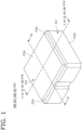
- FIG. 1 is a schematic perspective view illustrating the light-emitting device 200 according to the first embodiment.
- FIG. 2 is a schematic perspective view of the light-emitting device 200 shown in FIG. 1 without a cover 213.
- a metal film 221 and wirings 270 disposed on the upper surface of a light-emitting element 220 are omitted for convenience of description.
- FIG. 3 is a schematic top view of the light-emitting device 200 shown in FIG. 2 .
- FIG. 4 is a schematic cross-sectional view of the light-emitting device 200 taken along the cutting-plane line IV-IV of FIG. 1 .
- FIG. 5 is a schematic cross-sectional view of the light-emitting device 200 taken along the cutting-plane line V-V of FIG. 1 .
- the metal film 221 disposed on the upper surface of the light-emitting element 220 and a first metal film 232a, a second metal film 232b, and the wirings 270 disposed on the upper surface of a submount 230 are omitted for convenience of description.
- FIG. 6 is a schematic perspective view of a wavelength conversion portion 241 according to the present disclosure.
- FIG. 7 is a schematic perspective view of a wavelength conversion member 240 according to the present disclosure.
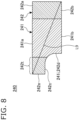
- FIG. 8 is a schematic cross-sectional view of the wavelength conversion member 240 taken along the cutting-plane line VIII-VIII of FIG. 7 .
- FIG. 9 is a schematic enlarged cross-sectional view of the light-emitting element 220, the wavelength conversion member 240, and the vicinity in the light-emitting device 200 shown in FIG. 5 .
- the metal film 221 disposed on the upper surface of the light-emitting element 220 and the first metal film 232a, the second metal film 232b, and the wirings 270 disposed on the upper surface of the submount 230 are omitted for convenience of description.
- FIG. 10 is a schematic enlarged top view of the light-emitting element 220, the wavelength conversion member 240, and the vicinity in the light-emitting device 200 shown in FIG. 3 .
- the light-emitting device 200 includes a base member 211, one or more light-emitting elements 220, and the wavelength conversion member 240.
- the light-emitting device 200 further includes a frame member 212, the cover 213, the submount 230, a protective element 250, and the wirings 270.
- the light-emitting device 200 does not necessarily include all of these components.
- the base member 211 has an upper surface 211a and a lower surface 211b.
- the base member 211 has a rectangular outer shape in a top view. This rectangular shape may be a rectangular shape having long sides and short sides.
- the base member 211 does not necessarily have a rectangular outer shape in a top view.
- the rectangular shape may include a square shape unless exclusion of a square shape is mentioned otherwise.
- the base member 211 can be formed of a metal as a main material.
- the metal to be used include copper and copper alloys.
- the base member 211 may be formed of a main material other than metals, such as a ceramic.
- the frame member 212 has an upper surface 212a, a lower surface 212b, one or more inner lateral surfaces 212c, and one or more outer lateral surfaces 212d.
- the frame member 212 has a rectangular frame shape in a top view.
- the one or more inner lateral surfaces 212c of the frame member 212 meet the upper surface 212a and extend downward from the upper surface 212a.
- the one or more outer lateral surfaces 212d of the frame member 212 meet the upper surface 212a and the lower surface 212b of the frame member 212.
- the frame member 212 may further include a stepped portion 214 having an upper surface 214a located above the upper surface 211a of the base member 211 and below the upper surface 212a of the frame member 212.
- the stepped portion 214 further has an inner lateral surface meeting the upper surface 214a and extending downward.
- the upper surface 214a meets one or more inner lateral surfaces 212c of the frame member 212.
- the upper surface 214a can be parallel to the upper surface 211a of the base member 211.
- the inner lateral surface of the stepped portion 214 meets the upper surface 211a of the base member 211.
- stepped portions 214 are respectively provided along two opposite inner lateral surfaces 212c in a top view.
- the stepped portion 214 may be provided along one inner lateral surface 212c.
- the frame member 212 does not necessarily include the stepped portion 214.
- the upper surface 214a of the stepped portion 214 may be provided with one or more metal films.
- the lower surface 211b of the base member 211 and/or the lower surface 212b of the frame member 212 may be provided with one or more metal films.
- the one or more metal films disposed on the upper surface 214a of the stepped portion 214 can be electrically connected to the metal films disposed on the lower surface 211b and/or the lower surface 212b through, for example, a via.
- Ni/Au metal films layered in the order of Ni and Au
- Ti/Pt/Au metal films layered in the order of Ti, Pt, and Au
- the stepped portion 214 can further has a lower surface 214b meeting the inner lateral surface of the stepped portion 214.
- the lower surface 214b can be a surface parallel to the upper surface 214a.
- the lower surface 214b is located above the lower surface 212b of the frame member 212.
- the lower surface 214b of the stepped portion 214 is bonded to the upper surface 211a of the base member 211.
- the frame member 212 further has a lateral surface meeting the lower surface 214b and extending downward.
- the lateral surface meets the lower surface 212b of the frame member 212.
- the lateral surface can be in contact with a lateral surface of the base member 211.
- the base member 211 and the frame member 212 define a recessed shape depressed in a direction from the upper surface 212a of the frame member 212 to the upper surface 211a of the base member 211.
- the recessed shape is formed at a location inward of the outer periphery of the frame member 212 in a top view.
- the upper surface 211a of the base member 211 is surrounded by a frame constituted of the one or more inner lateral surfaces 212c of the frame member 212 or/and the inner lateral surface of the stepped portion 214 in a top view.
- the outer shape of this frame is a rectangular shape having long sides and short sides.
- the base member 211 and the frame member 212 are separately formed and bonded together.
- the base member 211 and the frame member 212 may be integrally formed. This case will be described as a modified example.
- the frame member 212 can be formed of a material different from the material of the base member 211 as a main material.
- the main material constituting the frame member 212 include ceramics.
- the ceramics to be used include aluminum nitride, silicon nitride, aluminum oxide, and silicon carbide.
- the cover 213 has an upper surface 213a, a lower surface 213b, and one or more lateral surfaces 213c meeting the upper surface 213a and the lower surface 213b.
- the one or more lateral surfaces 213c connect the outer edges of the upper surface 213a and the outer edges of the lower surface 213b.
- the cover 213 has a rectangular parallelepiped or cubic shape.
- the upper surface 213a and the lower surface 213b of the cover 213 both have a rectangular shape, and the cover 213 has four rectangular lateral surfaces 213c.
- the cover 213 is not limited to a rectangular parallelepiped or cubic shape. That is, the cover 213 is not limited to a rectangular shape in a top view but may have any shape such as circles, ellipses, and polygons.
- the cover 213 is supported by the frame member 212.
- the cover 213 is disposed above the upper surface 211a of the base member 211.
- the outer peripheral portion of the lower surface 213b of the cover 213 is bonded to the upper surface 212a of the frame member 212.
- the cover 213 has a light-transmissive region that transmits light with a predetermined wavelength.
- the light-transmissive region constitutes at least a portion of the upper surface 213a and the lower surface 213b of the cover 213.
- the light-transmissive region of the cover 213 can be formed of sapphire as a main material.
- Sapphire is a material having a comparatively high transmittance and comparatively high strength.
- a material other than sapphire such as light-transmissive materials including quartz, silicon carbide, glass, or the like may be used.
- a portion other than the light-transmissive region of the cover 213 may be formed integrally with the light-transmissive region using the same material as the material of the light-transmissive region.
- a single light-emitting element 220 is mounted.
- a plurality of light-emitting elements may be mounted in the light-emitting device 200.
- the light-emitting element 220 is a semiconductor laser element.
- the light-emitting element 220 is not limited to a semiconductor laser element but may be, for example, a light-emitting diode (LED) or an organic light-emitting diode (OLED).
- LED light-emitting diode
- OLED organic light-emitting diode
- a semiconductor laser element is employed as the light-emitting element 220.
- the light-emitting element 220 has an elongated rectangular outer shape in a top view.
- a lateral surface meeting one of two short sides of the elongated rectangular shape serves as an emission end surface of light emitted from the light-emitting element 220.
- the upper surface and the lower surface of the light-emitting element 220 have larger areas than the area of the emission end surface.
- a metal film 221 may be disposed on the upper surface of the light-emitting element 220.
- the metal film 221 is provided with a wiring or the like for electrical connection to another member.
- the metal film 221 disposed on the upper surface of the light-emitting element 220 is not disposed over the entirety of the upper surface of the light-emitting element 220.
- the metal film 221 extends in the long side direction of the upper surface of the light-emitting element 220.
- the upper surface of the light-emitting element 220 is not necessarily provided with the metal film 221.
- the light-emitting element 220 is a semiconductor laser element
- Light (laser beam) radiated from the light-emitting element 220 exhibits divergence and an elliptic far-field pattern (hereinafter referred to as "FFP") in a plane parallel to an emission end surface.
- the FFP indicates the shape or light intensity distribution of emitted light at a position away from the emission end surface.
- a direction lying along the major axis of the elliptic shape is referred to as the fast axis direction of the FFP
- a direction lying along the minor axis of the elliptic shape is referred to as the slow axis direction of the FFP.
- the fast axis direction of the FFP of the light-emitting element 220 can correspond to the direction of layering of a plurality of semiconductor layers including an active layer of the light-emitting element 220.
- the main portion of light On the basis of the light intensity distribution of the FFP of the light-emitting element 220, light having an intensity of 1/e 2 or more of the peak intensity is referred to as the main portion of light.
- the angle corresponding to an intensity of 1/e 2 in the light intensity distribution is referred to as an angle of divergence.
- the angle of divergence in the fast axis direction of the FFP is larger than the angle of divergence in the slow axis direction of the FFP.
- Light at the center of the elliptic shape of FFP in other words, light with the peak intensity in the light intensity distribution of the FFP, is referred to as light traveling along an optical axis.
- An optical path of light traveling along the center of the elliptic FFP is referred to as the optical axis of the light.
- a light-emitting element that emits blue light can be used for the light-emitting element 220.
- the statement "light-emitting element that emits blue light” as used herein indicates that a light-emitting element to be used emits light with a peak emission wavelength within the range of 405 nm to 494 nm.
- a light-emitting element that emits light with a peak wavelength in a range of 430 nm to 480 nm is preferably used as the light-emitting element 220.
- Examples of such a light-emitting element 220 include a semiconductor laser element containing a nitride semiconductor.
- the nitride semiconductor for example, GaN, InGaN, or AlGaN can be used.
- the emission peak of light emitted from the light-emitting element 220 is not limited to the above.
- light emitted from the light-emitting element 220 can be visible light including green light and red light, ultraviolet light, or infrared light with wavelengths outside the above wavelength range, other than blue light.
- the submount 230 has a rectangular parallelepiped shape and has a lower surface, an upper surface, and one or more lateral surfaces.
- the width of the submount 230 is the smallest in the upper-lower direction.
- the shape of the submount 230 is not limited to a rectangular parallelepiped shape.
- the submount 230 is formed of aluminum nitride or silicon carbide but may be formed of another material.
- a first metal portion 231a is disposed on the upper surface of the submount 230, and a second metal portion 231b is disposed on the lower surface of the submount 230.
- the material constituting the first metal portion 231a and the second metal portion 231b include metals such as copper.
- the area of the first metal portion 231a is smaller than the area of the second metal portion 231b in a top view.
- the first metal portion 231a is disposed on a portion of the upper surface of the submount 230.
- the first metal portion 231a is not disposed on the entire upper surface of the submount 230. In the example shown in the drawings, the first metal portion 231a is rectangular in a top view.
- the first metal portion 231a is disposed along a portion in the long side direction of the elongated rectangular shape.
- the first metal portion 231a is located closer to one of two opposite short sides of the elongated rectangular shape than the other of the two opposite short sides.
- the second metal portion 231b is disposed on the lower surface of the submount 230.
- the second metal portion 231b is located directly below the entire first metal portion 231a with the submount 230 therebetween and located directly below at least a portion of the second metal film 232b described below in a top view.
- the first metal film 232a is further disposed on the first metal portion 231a.
- the first metal film 232a is disposed on a portion of the upper surface of the first metal portion 231a.
- the first metal film 232a is sandwiched between regions of the first metal portion 231a not provided with the first metal film 232a in a top view.
- the area of the first metal film 232a is smaller than the area of the regions of the first metal portion 231a not provided with the first metal film in a top view.
- the second metal film 232b is further disposed on a region of the upper surface of the submount 230 not provided with the first metal portion 231a.
- the area of the second metal film 232b is larger than the area of the first metal film 232a in a top view.
- the first metal film 232a and the second metal film 232b are formed of a metal such as gold.
- the metal portions and the metal films disposed on the submount 230 have been described. However, for example, a configuration may be employed in which the metal portions are not disposed and only the metal films are disposed. Providing the metal portions on the upper surface and the lower surface of the submount allows for improvement of the heat dissipation performance. In particular, heat generated from a member disposed directly above the first metal portion 231a can be efficiently dissipated.
- Each of the first metal portion 231a and the second metal portion 231b has a greater thickness than the thicknesses of a respective one of the first metal film 232a and the second metal film 232b in the direction perpendicular to the upper surface of the submount.
- the wavelength conversion member 240 includes the wavelength conversion portion 241 and a surrounding portion 242.
- the wavelength conversion portion 241 has an upper surface 241a, a lower surface 241b that is a surface opposite to the upper surface 241a, and a plurality of lateral surfaces.
- FIG. 6 is a schematic perspective view of an example of the wavelength conversion portion.
- the wavelength conversion portion 241 has an incident lateral surface 241i, a first lateral surface 241c, a second lateral surface 241d, a third lateral surface 241e, and a fourth lateral surface 241f as the lateral surfaces.
- the first lateral surface 241c, the second lateral surface 241d, the third lateral surface 241e, and the fourth lateral surface 241f are connected to the outer edges of the upper surface 241a and the outer edges of the lower surface 241b.
- the third lateral surface 241e is connected to each of the first lateral surface 241c and the fourth lateral surface 241f.
- the fourth lateral surface 241f is connected to the second lateral surface 241d and the third lateral surface 241e.
- the first lateral surface 241c is not connected to the fourth lateral surface 241f.
- the second lateral surface 241d is not connected to the third lateral surface 241e.
- a lateral side of the first lateral surface 241c and a lateral side of the second lateral surface 241d are connected to each other on upper portions thereof and are connected to the incident lateral surface 241i on lower portions thereof.
- the first lateral surface 241c and the second lateral surface 241d are connected to each other at a portion above the midpoint between the upper surface 241a and the lower surface 241b in the direction perpendicular to the upper surface 241a.
- the first lateral surface 241c and the second lateral surface 241d are connected to the incident lateral surface 241i at portions below the midpoint.
- the midpoint is the highest point of the incident lateral surface 241i.
- the lower side of the incident lateral surface 241i is connected to the outer edge of the lower surface 241b.
- the lower side of the incident lateral surface 241i is depressed inward from the portion at which the first lateral surface 241c and the second lateral surface 241d are connected.
- a lower side of the incident lateral surface 241i is depressed from the portion at which the first lateral surface 241c and the second lateral surface 241d are connected toward the portion at which the third lateral surface 241e and the fourth lateral surface 241f are connected.
- the first lateral surface 241c and the fourth lateral surface 241f may be parallel to each other in a top view.
- the second lateral surface 241d and the third lateral surface 241e may be parallel to each other in a top view.
- the first lateral surface 241c and the second lateral surface 241d, the first lateral surface 241c and the third lateral surface 241e, the third lateral surface 241e and the fourth lateral surface 241f, and the fourth lateral surface 241f and the second lateral surface 241d may be perpendicular to each other in a top view.
- the wavelength conversion portion 241 is to be irradiated with light. Accordingly, it is preferable that the base material of the wavelength conversion portion 241 be mainly formed of an inorganic material hardly decomposed by irradiation with light.
- the main material is a ceramic.
- the ceramic include aluminum oxide, aluminum nitride, silicon oxide, yttrium oxide, zirconium oxide, and magnesium oxide.
- a material having a melting point of 1,300°C to 2,500°C is preferably selected as the main material of the ceramic.
- main material of a specific member as used herein refers to a material constituting the largest proportion in the component on the basis of the mass or volume ratio. Also, the term “main material” as used herein may indicate that no other material is contained, that is, the main material alone constitutes the component.
- the wavelength conversion portion 241 may be formed of a material other than ceramics as the main material.
- the wavelength conversion portion 241 contains a phosphor.
- the wavelength conversion portion 241 can be formed by sintering a phosphor and aluminum oxide or the like.
- the content of the phosphor can be 0.05 vol% to 50 vol% relative to the total volume of the ceramic.
- a ceramic that is formed by sintering phosphor powder and consists substantially of the phosphor may be used.
- the wavelength conversion portion 241 may be formed of a single crystal of a phosphor.
- Examples of the phosphor include cerium-activated yttrium-aluminum-garnet (YAG), cerium-activated lutetium-aluminum-garnet (LAG), europium-activated silicate ((Sr,Ba) 2 SiO 4 ), ⁇ -SiAlON phosphors, and ⁇ -SiAlON phosphors.
- YAG phosphors have good heat resistance.
- the surrounding portion 242 has an upper surface 242a, a first lower surface 242b and a second lower surface 242c that are surfaces opposite to the upper surface 242a, a plurality of inner lateral surfaces connected to inner edges of the upper surface 242a and inner edges of the first lower surface 242b, and a plurality of outer lateral surfaces connected to outer edges of the upper surface 242a and outer edges of the first lower surface 242b and/or the outer edges of the second lower surface 242c.
- the surrounding portion 242 further has a connecting lateral surface 242d that meets the first lower surface 242b and is connected to the second lower surface 242c.
- the second lower surface 242c and the connecting lateral surface 242d are connected via a rounded edge portion in a lateral view.
- a plurality of inner lateral surfaces of the surrounding portion 242 preferably have a reflectance of light of 80% or more and 100% or less.
- the surrounding portion 242 is disposed around the wavelength conversion portion 241.
- the surrounding portion 242 covers the lateral surfaces of the wavelength conversion portion 241 except for the incident lateral surface 241i.
- the incident lateral surface 241i is not covered with the surrounding portion 242 but is exposed from the surrounding portion 242.
- the incident lateral surface 241i is connected to the connecting lateral surface 242d of the surrounding portion 242, and the incident lateral surface 241i and the connecting lateral surface 242d are in the same plane.
- a plurality of inner lateral surfaces of the surrounding portion 242 cover the first lateral surface 241c, the second lateral surface 241d, the third lateral surface 241e, and the fourth lateral surface 241f of the wavelength conversion portion 241.
- the upper surface 242a of the surrounding portion 242 and the upper surface 241a of the wavelength conversion portion 241 are in the same plane.
- the first lower surface 242b of the surrounding portion 242 and the lower surface 241b of the wavelength conversion portion 241 are in the same plane.
- the upper surface 242a and the upper surface 241a of the wavelength conversion portion 241 are not necessarily in the same plane.
- the first lower surface 242b of the surrounding portion 242 and the lower surface 241b of the wavelength conversion portion 241 is not necessarily in the same plane.
- the surrounding portion 242 further has a protrusion 242t.
- a portion of the surrounding portion 242 located above the incident lateral surface 241i and protruding outward relative to the incident lateral surface 241i in the direction perpendicular to the incident lateral surface 241i is referred to as the "protrusion 242t.”
- the protrusion 242t has at least a portion of the upper surface 242a of the surrounding portion 242, the second lower surface 242c, and a plurality of outer lateral surfaces connected to the upper surface 242a and the second lower surface 242c.
- the protrusion 242t does not have the first lower surface 242b.
- the surrounding portion 242 is divided into two portions by a plane that is parallel to the flat portion of the incident lateral surface 241i and passes through the portion at which the first lateral surface 241c and the second lateral surface 241d are connected, the protrusion 242t is a portion located on a side not in contact with the first lateral surface 241c or the second lateral surface 241d except for the connecting portion.
- the protrusion protrudes outward of the incident lateral surface 241i from one end to the other end of the wavelength conversion member 240 in a direction of a plane in which the incident lateral surface 241i and the connecting lateral surface 242d extend.
- an outer lateral surface oriented to the same direction as the incident lateral surface 241i and/or the connecting lateral surface 242d is referred to as a protruding surface 242e.
- the protruding surface 242e is parallel to the incident lateral surface 241i and the connecting lateral surface 242d.
- the protruding surface 242e is perpendicular to the first lower surface 242b and the upper surface 242a.
- parallel indicates that two surfaces of interest meet at an angle within ⁇ 5°.
- perpendicular indicates that two surfaces of interest meet at an angle of 85° or more and 95° or less. In any case, even in the case in which surfaces of interest do not meet each other but planes in which the respective surfaces extend intersect with each other, the intersection angle between the two planes can be regarded as the angle at which the two surfaces of interest meet.
- the surrounding portion 242 is a sintered body formed using a ceramic as a main material.
- the ceramic used as the main material include aluminum oxide, aluminum nitride, silicon oxide, yttrium oxide, zirconium oxide, and magnesium oxide.
- the surrounding portion 242 does not necessarily contain a ceramic as a main material.
- the surrounding portion 242 may be formed of a metal, a complex of a ceramic and a metal, or a resin.
- the wavelength conversion portion 241 and the surrounding portion 242 can be integrally formed.
- the wavelength conversion portion 241 and the surrounding portion 242 may be separately formed and bonded together to form the wavelength conversion member 240.
- the wavelength conversion portion 241 and the surrounding portion 242 constitute an integrated sintered body.
- the wavelength conversion member 240 may be provided with an anti-reflection film on the upper surface.
- the upper surface of the wavelength conversion member 240 herein refers to the upper surface 241a of the wavelength conversion portion 241 and/or the upper surface 242a of the surrounding portion 242.
- the upper surface of the wavelength conversion member 240 includes the upper surfaces 241a and 242a.
- the anti-reflection film can be disposed on the upper surface 241a of the wavelength conversion portion 241 and/or the upper surface 242a of the surrounding portion 242.
- the lower surface of the wavelength conversion member 240 is provided with a metal film.
- the lower surface of the wavelength conversion member 240 herein refers to the lower surface 241b of the wavelength conversion portion 241 and/or the first lower surface 242b of the surrounding portion 242.
- the lower surface of the wavelength conversion member 240 includes the lower surface 241b and the first lower surface 242b.
- the lower surface of the wavelength conversion member 240 does not include the second lower surface 242c of the surrounding portion 242.
- a metal film may be disposed on the lower surface 241b of the wavelength conversion portion 241 and/or the first lower surface 242b of the surrounding portion 242.
- the incident lateral surface 241i of the wavelength conversion member 240 may be provided with a reflective film.
- the protective element 250 is a component for protecting a specific element such as a semiconductor laser element.
- the protective element 250 is a component for preventing an excessive current from flowing through and breaking a specific element such as a semiconductor laser element.
- a Zener diode formed of Si can be used as the protective element 250.
- the protective element 250 may be a component for measuring the temperature to prevent a specific element from breaking due to the temperature environment.
- a thermistor can be used as such a temperature measuring element.
- the temperature measuring element is preferably disposed near the emission end surface of the light-emitting element 220.
- the wirings 270 are each constituted of a linear electric conductor with both ends serving as bonding portions.
- the wiring 270 includes bonding portions bonded to other components at both ends of the linear portion.
- the wiring 270 is used to electrically connect two components.
- a metal wire can be used for the wiring 270. Examples of the metal include gold, aluminum, silver, copper, and tungsten.
- the light-emitting device 200 is described.
- the one or more light-emitting elements 220 are disposed on the upper surface 211a of the base member 211.
- a single light-emitting element 220 is disposed on the upper surface 211a.
- the lateral sides of the light-emitting element 220 are further surrounded by the frame member 212 in a top view viewed in a direction perpendicular to the upper surface 211a of the base member 211.
- the "top view” refers to a “top view” viewed in the direction perpendicular to the upper surface 211a of the base member 211 unless otherwise noted.
- the light-emitting element 220 emits light traveling in a lateral direction.
- the light emitted from the light-emitting element 220 is blue light.
- the light emitted from the light-emitting element 220 is not limited to blue light.
- the light-emitting element 220 is a semiconductor laser element.
- the light-emitting element 220 is mounted on the submount 230 disposed on the upper surface 211a of the base member 211. More specifically, the light-emitting element 220 is disposed in a region in which the first metal portion 231a disposed on the upper surface of the submount 230 is disposed. Still more specifically, the light-emitting element 220 is bonded to the first metal film 232a disposed on the first metal portion 231a with, for example, a metal adhesive therebetween.
- the lower surface of the submount 230 provided with the second metal portion 231b is bonded to the upper surface 211a of the base member 211 with, for example, a metal adhesive therebetween. Examples of the metal adhesive used for the bonding include AuSn.
- the light-emitting element 220 is disposed such that the emission end surface is oriented to the same direction as one of the lateral surfaces of the submount 230.
- the emission end surface of the light-emitting element 220 can be parallel/perpendicular to one of the inner lateral surfaces 212c or one of the outer lateral surfaces 212d of the frame member 212.
- the wavelength conversion member 240 is disposed on the upper surface 211a of the base member 211.
- the wavelength conversion member 240 is disposed in the lateral direction of the light-emitting element 220. More specifically, the wavelength conversion member 240 is located at a position on which light that is emitted from the light-emitting element 220 and travels in the lateral direction is incident. Furthermore, the wavelength conversion member 240 is located on the optical axis of the light emitted in the lateral direction from the light-emitting element 220. In the example shown in the drawings, the direction of the optical axis of the emitted light is not converted from the emission of the light from the light-emitting element 220 until the incidence on the wavelength conversion portion 241 of the wavelength conversion member 240.
- the wavelength conversion member 240 is disposed on the upper surface 211a of the base member with the submount 230 therebetween.
- the wavelength conversion member 240 is disposed on the submount on which the light-emitting element 220 is disposed. Disposing the light-emitting element 220 and the wavelength conversion member 240 on the same submount 230 allows the light-emitting element 220 and the wavelength conversion member 240 to be disposed closely to each other. This allows the emitting light that is emitted from the light-emitting element 220 and has divergence to efficiently enter the wavelength conversion member 240, leading to reduction in the size of the light-emitting device 200.
- the wavelength conversion member 240 may be disposed on a submount different from the submount on which the light-emitting element 220 is disposed.
- the upper surface of the submount, on which the wavelength conversion member 240 is disposed is not positioned higher than the lower surface of the light-emitting element 220.
- the wavelength conversion member 240 is disposed in a region of the upper surface of the submount 230 not provided with the first metal portion 231a. More specifically, the metal film disposed on the lower surface of the wavelength conversion member 240 and the second metal film 232b disposed on the upper surface of the submount 230 are bonded together with, for example, a metal adhesive therebetween. Examples of the metal adhesive include AuSn. A portion of the second metal portion 231b is disposed in at least a portion of a region of the lower surface of the submount 230 located directly below the wavelength conversion member 240. In other words, the lower surface of the wavelength conversion member 240 and the second metal film 232b overlap with the second metal portion 231b in a top view.
- the wavelength conversion member 240 has an incident lateral surface on which light that is emitted from the emission end surface of the light-emitting element 220 and travels in the lateral direction is incident, and an exit surface that emits light obtained by wavelength conversion of the incident light.
- the incident lateral surface 241i and the upper surface 241a of the wavelength conversion portion 241 respectively serve as the incident lateral surface and the exit surface.
- Light emitted from the light-emitting element is wavelength-converted by the wavelength conversion portion 241 and is emitted upward from the upper surface 241a of the wavelength conversion portion 241.
- the surrounding portion 242 of the wavelength conversion member 240 is disposed around the wavelength conversion portion 241.
- the surrounding portion 242 reflects light that has entered the wavelength conversion portion 241 and has been incident on the inner lateral surfaces of the surrounding portion 242.
- the light reflected by the surrounding portion 242 travels inside the wavelength conversion portion 241. This structure allows light incident on the incident lateral surface 241i to be efficiently emitted from the upper surface 241a, which is the exit surface.
- an intersection between an extension of the side at which the first lateral surface 241c meets the lower surface 241b of the wavelength conversion portion 241 and an extension of the side at which the second lateral surface 241d meets the lower surface 241b is located on a second direction side (as defined below), which is the side opposite to the direction of travel of light, with respect to the incident lateral surface 241i.
- the two extensions intersect with each other on the second direction side, that is, the light-emitting element 220 side, with respect to the incident lateral surface 241i.
- the third lateral surface 241e and the fourth lateral surface 241f of the wavelength conversion portion 241 meet each other in a first direction, which is the side of the direction of travel of light, that is, on the side opposite to the light-emitting element 220, with respect to the incident lateral surface 241i.
- first direction side and the term “second direction side” are described.
- the direction in which light traveling along the optical axis of the light emitted from the light-emitting element 220 is referred to as the first direction.
- the direction in which light traveling along the optical axis of the light emitted from the light-emitting element 220 and a virtual line OA, which is a virtual extension of the optical axis, travels is regarded as the "first direction”.
- the wavelength conversion member 240 is located on the first direction side with respect to the light-emitting element 220, and the light-emitting element 220 is located on the second direction side with respect to the wavelength conversion member 240.
- the protrusion 242t of the surrounding portion 242 included in the wavelength conversion member 240 protrudes on the second direction side (light-emitting element 220 side) with respect to the incident lateral surface 241i.
- the protrusion 242t protrudes on the second direction side (light-emitting element 220 side) with respect to the end of the lower surface of the wavelength conversion member 240 on the second direction side (light-emitting element 220 side).
- the protrusion 242t protrudes on the second direction side (light-emitting element 220 side) with respect to the end(s) of the lower surface 241b of the wavelength conversion portion 241 and/or the first lower surface 242b of the surrounding portion 242 on the light-emitting element side.
- the protrusion 242t overlaps with an emission end surface 220a of the light-emitting element 220 in a top view. More specifically, the emission end surface 220a overlaps with the second lower surface 242c of the protrusion 242t in a top view.
- the protruding surface 242e of the protrusion 242t is located on the second direction side with respect to the emission end surface 220a.
- the emission end surface 220a of the light-emitting element 220 is hidden by the protrusion 242t in a top view.
- the main portion of light emitted from the light-emitting element 220 travels in the lateral direction and enters the wavelength conversion portion 241. More specifically, the incident lateral surface 241i includes the region in which the wavelength conversion portion 241 is irradiated with the main portion of light emitted from the light-emitting element 220.
- the wavelength conversion portion 241 performs wavelength conversion of incident light and emits wavelength-converted light upward from the upper surface 241a.
- a portion of light that has leaked out of the active layer of the light-emitting element 220 and/or a portion of light other than the main portion of light emitted from the light-emitting element 220 can be leaking light traveling upward from the emission end surface 220a and the vicinity.
- the leaking light does not enter the wavelength conversion portion 241 but travels upward without being subjected to wavelength conversion.
- the protrusion 242t of the surrounding portion 242 by disposing the protrusion 242t of the surrounding portion 242 to overlap with the emission end surface 220a of the light-emitting element 220 in a top view, the protrusion 242t reflects the leaking light traveling upward, thereby suppressing emission of the leaking light out of the light-emitting device 200. It is possible to inhibit the leaking light that does not enter the wavelength conversion portion 241 from being mixed into light that enters the wavelength conversion portion 241 and is emitted from the light-emitting device 200. It is thus possible to provide the light-emitting device 200 in which the effect of light not used as the emitting light of the light-emitting element 220 on light that enters the wavelength conversion member 240 and is extracted is suppressed.
- the protrusion 242t preferably overlaps with the entire emission end surface 220a of the light-emitting element 220 in a top view.
- the protruding surface 242e is located at a side toward the second direction with respect to the emission end surface 220a in a top view.
- the protruding surface 242e is longer than the entirety of the emission end surface 220a in a direction parallel to the emission end surface 220a in a top view.
- the protrusion 242t preferably overlaps with the emission end surfaces 220a of all the light-emitting elements 220 in a top view. It is thus possible to reduce leaking light traveling upward from the emission end surfaces 220a of all the light-emitting elements 220.
- the protrusion 242t overlaps with the entire emission end surface 220a of each light-emitting element 220 in a top view. Specifically, the protruding surface 242e is located on the second direction side with respect to the whole of each emission end surface 220a.
- the protruding surface 242e is longer in the direction parallel to the emission end surface 220a in a top view than a straight line connecting the endpoints of each of the emission end surfaces 220a of the light-emitting elements at both ends among a plurality of light-emitting elements 220. Although not shown in the drawings, the protruding surface 242e is longer than the longest one of the "straight lines connecting the endpoints" described above.
- the case in which the light emitted from the light-emitting element 220 is blue light is described as a specific example.
- the main portion of light emitted from the light-emitting element 220 is emitted in the lateral direction and enters the wavelength conversion portion 241.
- a portion of the light that has entered the wavelength conversion portion 241 is subjected to wavelength conversion into, for example, yellow light and is emitted from the upper surface 241a of the wavelength conversion portion 241.
- the yellow light is mixed with blue light that has entered the wavelength conversion portion 241, has not been wavelength-converted, and has been emitted from the upper surface 241a to constitute, for example, white light that is emitted from the light-emitting device 200.
- leaking light incident upward from the emission end surface 220a of the light-emitting element 220 is blue light and can be emitted from the light-emitting device 200 and mixed with the white light.
- the white light mixed with the leaking light may show unevenness in color.
- the wavelength conversion portion 241 is disposed such that the optical axis of the light emitted from the light-emitting element 220 passes through the incident lateral surface 241i in a top view as shown in FIG. 7 and FIG. 8 .
- the upper surface 241a of the wavelength conversion portion 241 may be symmetric about the virtual line OA lying along the optical axis up to the incidence on the incident lateral surface 241i in a top view.
- the upper surface of the surrounding portion 242 may be symmetric about the virtual line OA in a top view.
- the virtual line OA passes through the midpoint of the incident lateral surface 241i in the direction perpendicular to the upper surface 211a and meets one of the inner lateral surfaces 212c of the frame member 212.
- the portion of the frame member 212 meeting the virtual line OA and the vicinity constitutes a light-shielding portion formed of a material that absorbs light
- light is absorbed by the light-shielding portion, which allows for reduction of the possibility of emission of the light out of the light-emitting device 200.
- a length L1 from the center of the wavelength conversion portion 241 to the tip of the protrusion 242t is greater than a length L2 from the center of the wavelength conversion portion 241 to an end of the surrounding portion 242 opposite to the protrusion 242t in a top view.
- the term "center of the wavelength conversion portion 241" as used herein refers to the midpoint of a line segment connecting the intersection point of the first lateral surface 241c and the second lateral surface 241d and the intersection point of the third lateral surface 241e and the fourth lateral surface 241fin a top view.
- the tip of the protrusion 242t refers to any point selected from the side at which the protruding surface 242e and the upper surface 242a meet each other.
- Making the length L1 longer than the length L2 allows for increase in the length of the protrusion 242t from the emission end surface 220a on the second direction side while maintaining the length of the wavelength conversion portion 241 in the virtual line OA direction, so that it is possible to further reduce leaking light emitted out of the light-emitting device 200.
- the length L1 may be equal to the length L2.
- a length L3 from the emission end surface 220a of the light-emitting element 220 to the tip of the protrusion 242t is preferably 0 ⁇ m or more and 400 ⁇ m or less in the direction parallel to the virtual line OA in a top view. Setting the length L3 to 0 ⁇ m or more allows the protrusion 242t to overlap with the emission end surface 220a and allows for reduction of leaking light. Setting the length L3 to 400 ⁇ m or less allows a region in which the wiring 270 for connection to the light-emitting element 220 is disposed to be secured.
- the light emitted from the light-emitting element 220 travels toward the wavelength conversion member 240 and is incident on the incident lateral surface 241i of the wavelength conversion portion 241 exposed from the surrounding portion 242. At least a portion of the incident lateral surface 241i of the wavelength conversion portion 241 is located below the virtual line OA.
- This structure allows for light traveling below the virtual line OA out of the light emitted from the light-emitting element 220 to be efficiently introduced from the incident lateral surface 241i into the wavelength conversion portion 241.
- Light is emitted from the upper surface 241a of the wavelength conversion portion 241 on the basis of the light incident on the incident lateral surface 241i.
- the term "light emitted on the basis of the incident light” as used herein refers to, for example, incident light or for example, light obtained by wavelength conversion of the incident light.
- the emission end surface 220a of the light-emitting element 220 faces the incident lateral surface 241i of the wavelength conversion portion 241.
- the emission end surface 220a of the light-emitting element 220 is parallel to the incident lateral surface 241i of the wavelength conversion portion 241.
- length between the incident lateral surface 241i of the wavelength conversion portion 241 and the emission end surface 220a is 20 ⁇ m or more and 1,000 ⁇ m or less.
- the length between the incident lateral surface 241i and the end of the protrusion 242t on the second direction side (light-emitting element 220 side) is 50 ⁇ m or more and 800 ⁇ m or less and is more preferably 100 ⁇ m or more and 500 ⁇ m or less.
- One of the two lateral surfaces of the light-emitting element 220 meeting the emission end surface 220a faces one of the two opposite inner lateral surfaces 212c or the lateral surface of the stepped portion 214 provided along the one inner lateral surface 212c.
- one of the two lateral surfaces of the light-emitting element 220 meeting the emission end surface 220a is parallel to one of the inner lateral surfaces 212c or the lateral surface of the stepped portion 214 provided along the one inner lateral surface 212c.
- the other one of the two lateral surfaces of the light-emitting element 220 meeting the emission end surface faces the other inner lateral surface 212c or the lateral surface of the stepped portion 214 provided along the other inner lateral surface 212c.
- the other one of the two lateral surfaces of the light-emitting element 220 meeting the emission end surface is parallel to the other inner lateral surface 212c or the lateral surface of the stepped portion 214 provided on the other inner lateral surface 212c.
- the upper surface 214a of the stepped portion 214 is located below the height of the upper surface 241a of the wavelength conversion portion 241 on the basis of the upper surface 211a of the base member 211. With such heights, light emitted upward from the upper surface 241a is prevented from being directly applied to the stepped portion 214.
- the upper surface 214a of the stepped portion 214 is located above the height of the upper surface of the light-emitting element 220 on the basis of the upper surface 211a of the base member 211.
- the wirings 270 electrically connect the light-emitting element 220 and the protective element 250 to the base member 211 and/or the frame member 212.
- the wirings 270 in the light-emitting device 200 are shown in the drawings as an example in which the protective element 250 is a Zener diode, but wiring connections different from the connections shown in the drawings may be employed in the case in which the protective element 250 is a temperature measuring element.
- the light-emitting element 220 is electrically connected to the metal film disposed on the upper surface 214a of the stepped portion 214 via the wiring 270.
- one end of the wiring 270 is bonded to the metal film 221 disposed on the upper surface of the light-emitting element 220.
- the light-emitting device 200 includes a plurality of wirings 270.
- the wirings 270 include a wiring 270 having one of both ends bonded to the upper surface 214a of the stepped portion 214 and the other end bonded to the submount 230.
- the other end is bonded to the upper surface of the first metal portion 231a disposed on the submount.
- the wiring 270 for connection to the light-emitting element 220 is bonded to the upper surface of the light-emitting element 220 and the metal film disposed on the upper surface 214a of the stepped portion 214 on the second direction side (side opposite to the wavelength conversion member 240) with respect to the center of the light-emitting element 220. Disposing the wiring 270 for connection to the light-emitting element 220 in this manner allows for increase of the region in which the wiring 270 does not overlap with the protrusion 242t in a top view and therefore allows for increase of the protrusion amount of the protrusion 242t on the second direction side (light-emitting element 220 side).
- the metal film disposed on the lower surface 211b of the base member 211 can be used for the electrical connection between the light-emitting element 220 and an external power source.
- This structure allows the light-emitting element 220 to be electrically connected to the external power source via the metal film on the upper surface 212a of the frame member 212 electrically connected via a metal material disposed in a via hole to the metal film disposed on the upper surface 214a of the stepped portion 214.
- the cover 213 is disposed on the upper surface 212a of the frame member 212. Specifically, the cover 213 is supported by the upper surface 212a of the frame member 212 and is disposed above the light-emitting element 220 surrounded by the frame member 212. For example, the outer peripheral portion of the lower surface of the cover 213 is bonded to the upper surface 212a of the frame member 212. For example, the metal film disposed on the outer peripheral portion of the lower surface of the cover 213 is bonded and fixed via Au-Sn or the like to the metal film disposed on the upper surface 212a of the frame member 212.
- the cover 213 is bonded to the upper surface 212a of the frame member 212 to define a sealed space in which the light-emitting element 220 and the wavelength conversion member 240 are disposed.
- the sealed space may be defined in a hermetically sealed state. Hermetically sealing the sealed space allows for suppression of dust collection of organic matter and the like on the emission end surface 220a of the light-emitting element 220.
- the cover 213 has the light-transmissive region that transmits light emitted from the upper surface 241a of the wavelength conversion portion 241 to emit the light to the outside. That is, light emitted from the upper surface 241a of the wavelength conversion portion 241 on the cover 213 side may be transmitted through the light-transmissive region of the cover 213 and emitted out of the light-emitting device 200.
- the entirety of the cover 213 may be the light-transmissive region.
- the light-transmissive region of the cover 213 transmits 70% or more of light emitted from the light-emitting element 220 and light emitted from the wavelength conversion member 240.
- a light-emitting device 201 according to a modified example is described with reference to FIG. 1 to FIG. 3 and FIG. 11 .
- FIG. 1 is a schematic perspective view of the light-emitting device 201 according to a modified example of the first embodiment.
- FIG. 2 is a schematic perspective view of the light-emitting device 201 shown in FIG. 1 without the cover 213.
- FIG. 3 is a schematic top view of the light-emitting device 201 shown in FIG. 2 .
- FIG. 11 is a schematic cross-sectional view of the light-emitting device 201 taken along the cutting-plane line XI-XI of FIG. 1 .
- the base member 211 and the frame member 212 are integrally formed.
- the base member 211 has a projection 211t on the upper surface 211a side.
- the upper surface 211a of the base member 211 includes the upper surface of the projection 211t and an upper surface located below the upper surface of the projection 211t.
- the light-emitting element 220 is directly disposed on the upper surface of the projection 211t.
- the wavelength conversion member 240 is directly disposed on the upper surface located below the upper surface of the projection 211t.
- the light-emitting element 220 and the wavelength conversion member 240 are not disposed on the submount.
- the base member 211 does not necessarily have the projection 211t.
- Examples of the main material used for the base member 211 and the frame member 212 integrally formed include ceramics.
- Examples of the ceramics include aluminum nitride, silicon nitride, aluminum oxide, and silicon carbide.
- the main material constituting the base member 211 and the frame member 212 is not limited to a ceramic but may be, for example, a metal such as copper.
- a light-emitting device 300 according to a second embodiment is described with reference to FIG. 1 , FIG. 12 , and FIG. 13 .
- the light-emitting device 300 according to the second embodiment differs from the light-emitting device 200 according to the first embodiment in that the light-emitting device 300 includes a light-transmissive member 313 provided with a light-shielding film 380 on a lower surface 313b of the light-transmissive member 313.
- FIG. 1 is a schematic perspective view of the light-emitting device 300 according to the second embodiment and a light-emitting device 301 according to a modified example of the second embodiment.
- FIG. 12 is a schematic enlarged cross-sectional view of the light-emitting element 220, the wavelength conversion member 240, the light-transmissive member 313, and the vicinity in the light-emitting device 300 according to the second embodiment taken along the cutting-plane line XII-XII of FIG. 1 .
- FIG. 12 is a schematic enlarged cross-sectional view of the light-emitting element 220, the wavelength conversion member 240, the light-transmissive member 313, and the vicinity in the light-emitting device 300 according to the second embodiment taken along the cutting-plane line XII-XII of FIG. 1 .
- FIG. 13 is a schematic enlarged cross-sectional view of the light-emitting element 220, the wavelength conversion member 240, the light-transmissive member 313, and the vicinity in the light-emitting device 301 according to the modified example of the second embodiment taken along the cutting-plane line XIII-XIII of FIG. 1 .
- the light-transmissive member 313 is formed of a light-transmissive main material.
- the term "light-transmissive" as used herein indicates that the transmittance of light having a specific wavelength is 80% or more.
- Examples of the main material constituting the light-transmissive member 313 include sapphire and glass made of silicon oxide or silicon nitride.
- the light-transmissive member 313 has an upper surface, the lower surface 313b, and one or more lateral surfaces meeting the upper surface and the lower surface 313b.
- the one or more lateral surfaces connect the outer edges of the upper surface and the outer edges of the lower surface 313b.
- the light-transmissive member 313 has a rectangular parallelepiped shape.
- the shape of the light-transmissive member 313 is not limited to a rectangular parallelepiped but can be, for example, a prism.
- the light-transmissive member 313 is disposed above the wavelength conversion member 240 and the light-emitting element.
- the light-transmissive member 313 is supported by the frame member 212. More specifically, the lower surface 313b of the light-transmissive member 313 is bonded to the upper surface 212a of the frame member 212.
- the light-transmissive member 313 may be referred to as a "cover.”
- the "cover” in this case is identical to the "cover 213" in the first embodiment.
- the light-transmissive member 313, the frame member 212, and the base member 211 define a sealed space in which the light-emitting element 220 and the wavelength conversion member 240 are sealed.
- the light-shielding film 380 can be disposed on the upper surface and/or the lower surface 313b of the light-transmissive member 313. In the example shown in FIG. 12 and FIG. 13 , the light-shielding film 380 is disposed on the lower surface 313b of the light-transmissive member 313.
- the light-shielding film 380 is formed of a member that reflects or absorbs incident light.
- the light-shielding film 380 can be a metal film formed of a metal. Examples of the metal used for the metal film include titanium, aluminum, gold, silver, copper, platinum, chromium, nickel, iron, zinc, cobalt, palladium, tantalum, tungsten, and an alloy containing one or more selected from these metals.
- the member used as the light-shielding film 380 is not limited to a metal film but can be a member that reflects or absorbs light, such as a dielectric film and a dielectric multilayer film made of a resin or an oxide such as SiO 2 , Ta 2 O 5 , and TiO 2 .
- the light-emitting device 300 according to the second embodiment is described. Descriptions overlapping with the descriptions of the first embodiment are omitted as appropriate, and the light-shielding film 380 and the wavelength conversion member 240 are mainly described.
- the protrusion 242t of the wavelength conversion member 240 overlaps with the emission end surface 220a of the light-emitting element 220 in a top view.
- at least a portion of the light-shielding film 380 disposed on the lower surface 313b of the light-transmissive member 313 overlaps with the protrusion 242t.
- the portion of light is reflected/absorbed by the light-shielding film 380 and is inhibited from being emitted out of the light-emitting device 300. Unevenness in color is therefore reduced, and it is possible to provide the light-emitting device 300 that emits highly uniform light.
- the emission end surface 220a of the light-emitting element 220 does not overlap with the light-shielding film 380 in a top view.
- the lower surface 313b of the light-transmissive member 313 has a light-shielding region provided with the light-shielding film 380 and a light-transmissive region not provided with the light-shielding film 380.
- the light-transmissive region transmits light emitted from the upper surface 241a of the wavelength conversion portion 241.
- the light-shielding region is located on a virtual straight line V1 (hereinafter referred to as a virtual line V1) connecting any point on the side at which the emission end surface 220a and the upper surface of the light-emitting element 220 meet each other and the end of the protrusion 242t in a lateral view as shown in FIG. 12 .
- the light-transmissive region is not located on the virtual line V1. Disposing the light-shielding film 380 at such a position allows for suppression of emission of light from an unintended region of the light-emitting device 300. At least the majority of the light-shielding region of the lower surface 313b of the light-transmissive member 313 is located on the second direction side (light-emitting element 220 side) with respect to the virtual line V1. The light-shielding region and the light-transmissive region are located in this order on the first direction side (wavelength conversion member 240 side) with respect to the virtual line V1. The light-shielding region is not necessarily provided on the first direction side (wavelength conversion member 240 side) with respect to the virtual line V1.
- the light-shielding region may be located on a straight line connecting any point that is on the upper surface of the light-emitting element 220 and is 30 ⁇ m or more away from the emission end surface 220a in the virtual line OA direction and the end of the protrusion 242t. Disposing the light-shielding region at such a position allows for further improvement of the shielding of leaking light from the vicinity of the emission end surface 220a.
- the light-emitting device 301 shown in FIG. 13 differs from the light-emitting device 300 according to the second embodiment in that the protrusion 242t of the wavelength conversion member 240 does not overlap with the emission end surface 220a of the light-emitting element 220 in a top view.
- the protrusion 242t of the wavelength conversion member 240 does not overlap with the emission end surface 220a of the light-emitting element 220 in a top view.
- at least a portion of the light-shielding film 380 overlaps with the protrusion 242t of the wavelength conversion member 240 in a top view.
- the emission end surface 220a of the light-emitting element 220 overlaps with the light-shielding film 380 in a top view.
- the light-shielding region provided with the light-shielding film 380 is located at a position through which a virtual straight line V2 (hereinafter referred to as a virtual line V2) passes.
- the virtual line V2 connects the upper end of the emission end surface 220a of the light-emitting element 220 and the upper end of the lateral surface of the protrusion 242t located at the extreme end on the second direction side (light-emitting element 220 side).
- the light-transmissive region is not located on the virtual line V2.
- the light-shielding region of the lower surface 313b of the light-transmissive member 313 is located on the second direction side (light-emitting element 220 side) with respect to the virtual line V2.
- the light-shielding region and the light-transmissive region are located in this order on the first direction side (wavelength conversion member 240 side) with respect to the virtual line V2.
- the light-shielding region is not necessarily located on the first direction side (wavelength conversion member 240 side) with respect to the virtual line V2.
- Disposing the light-shielding film 380 at such a position allows for suppression of emission of leaking light out of the light-emitting device 301 even in the case in which the protrusion 242t does not overlap with the emission end surface 220a of the light-emitting element 220 in a top view. Unevenness in color is therefore reduced, and it is possible to provide the light-emitting device 301 that emits highly uniform light. It is also possible to improve the safety of the light-emitting element 220.
- the light-shielding film 380 does not overlap with the upper surface 241a of the wavelength conversion portion 241 in a top view.
- the wavelength conversion portion 241 overlaps with the light-transmissive region, and the wavelength conversion portion 241 does not overlaps with the light-shielding region.
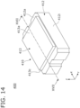
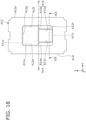
- the light emitting device 400 is different from the light emitting devices 200 and 300 according to other embodiments in that inner lateral surfaces of the frame member 412 have a stepped shape in a top plan view.
- FIG. 14 is a schematic perspective view illustrating an example of a light emitting device 400.
- FIG. 15 is a schematic perspective view illustrating an internal structure of the light emitting device 400.
- illustration of wirings 270, shown in FIG. 16 are omitted in FIG. 15 .
- FIG. 16 is a schematic top view illustrating the internal structure of the light emitting device 400.
- FIG. 17 is a schematic cross-sectional view taken along the line XVII-XVII in FIG. 14 and illustrating the example of the light emitting device 400.
- FIG. 18 is a schematic top view illustrating a base member 411 and a frame member 412.
- FIG. 19 is a schematic cross-sectional view taken along the line XIX-XIX in FIG.
- FIG. 20 is a schematic top view corresponding to FIG. 16 for describing further details of a wavelength conversion member 240 and a light emitting element 220 of the light emitting device 400.
- FIG. 21 is a schematic cross-sectional view corresponding to FIG. 17 for describing further details of the wavelength conversion member 240 and the light emitting element 220 of the light emitting device 400.
- an X-axis, a Y-axis, and a Z-axis orthogonal to each other are illustrated for reference.
- Directions parallel to the X-axis, the Y-axis, and the Z-axis are defined as an X-axis direction, a Y-axis direction, and a Z-axis direction, respectively.
- the X-axis direction and the Y-axis direction are parallel to the upper surface 411a of the base member 411, and the Z-axis direction is perpendicular to the upper surface 411a of the base member 411.
- the package 410 includes the base member 411, the frame member 412, and a cover 413.
- the base member 411 has the upper surface 411a and a lower surface 411b.
- the base member 411 has a rectangular outer shape in the top view.
- the rectangle may be a rectangle having long sides and short sides.
- the outer shape of the base member 411 in the top view is not necessarily rectangular.
- the term "rectangle" in the present specification also includes a square unless specifically stated to exclude a square.
- the frame member 412 is connected to the upper surface 411a of the base member 411 and extends upward from the upper surface 411a.
- the frame member 412 has one or more upper surfaces, a first lower surface 412b, a plurality of inner lateral surfaces, and one or more outer lateral surfaces 412i.
- the one or more upper surfaces of the frame member 412 include a first upper surface 412a meeting the one or more outer lateral surfaces 412i.
- the outer perimeter shape of the first upper surface 412a is, for example, rectangular.
- the inner perimeter shape of the first upper surface 412a is, for example, a rectangle.
- a plurality of inner lateral surfaces of the frame member 412 meet the upper surface 411a of the base member 411.
- the base member 411 and the frame member 412 form a recess depressed from the first upper surface 412a of the frame member 412 toward the upper surface 411a of the base member 411.
- the recess is formed at a location inward of an outer periphery of the frame member 412 in the top view.
- the upper surface 411a of the base member 411 is surrounded by a frame formed by a plurality of inner lateral surfaces of the frame member 412.
- the shape of the frame is a rectangle having long sides and short sides.
- the base member 411 and the frame member 412 are formed separately and bonded together. Alternatively, the base member 411 and the frame member 412 may be formed together as a single seamless piece.
- stepped portions are formed inside the frame member 412.
- the frame member 412 has a first stepped portion 414 and/or a second stepped portion 415 that are step-shaped in the top view.
- the frame member 412 has a second upper surface 414a and a third upper surface 415a along the two edges, extending in the X-axis direction, of the inner perimeter of the first upper surface 412a.
- the second upper surface 414a extends along one of the two edges, extending in the X direction, of the first upper surface 412a.
- the third upper surface 415a extends along the other of the two edges, extending in the X direction, of the first upper surface 412a.
- the second upper surface 414a and the third upper surface 415a of the frame member 412 do not extend over the entire length of the two respective edges extending in the X-axis direction.
- the second upper surface 414a and the third upper surface 415a extend along only a portion of the two respective edges extending in the X-axis direction. In the illustrated example, both the second upper surface 414a and the third upper surface 415a are provided toward the negative X direction in the X-axis direction.
- the frame member 412 further has one or more inner lateral surfaces meeting the second upper surface 414a and extending downward.
- the one or more inner lateral surfaces include a first inner lateral surface 412c that meets the second upper surface 414a.
- the first inner lateral surface 412c meets the upper surface 411a of the base member 411.
- the plurality of edges at which the first inner lateral surface 412c and the second upper surface 414a meet each other include an edge extending in the X-axis direction and an edge extending in the Y-axis direction in the top view.
- a curved line is further provided between the edge extending in the X-axis direction and the edge extending in the Y-axis direction.
- edges at which the first inner lateral surface 412c and the upper surface 411a of the base member 411 meet each other include an edge extending in the X-axis direction and an edge extending in the Y-axis direction in the top view.
- a curved line is further provided between the edge extending in the X-axis direction and the edge extending in the Y-axis direction.
- the first inner lateral surface 412c does not meet the first upper surface 412a.
- the frame member 412 has one or more inner lateral surfaces meeting the third upper surface 415a and extending downward.
- the one or more inner lateral surfaces include a second inner lateral surface 412d meeting the third upper surface 415a.
- the second inner lateral surface 412d meets the upper surface 411a of the base member 411.
- the plurality of edges at which the second inner lateral surface 412d and the third upper surface 415a meet each other include an edge extending in the X-axis direction and an edge extending in the Y-axis direction in the top view.
- a curved line is further provided between the edge extending in the X-axis direction and the edge extending in the Y-axis direction.
- the edges at which the second inner lateral surface 412d and the upper surface 411a of the base member 411 meet each other include an edge extending in the X-axis direction and an edge extending in the Y-axis direction in the top view.
- a curved line is further provided between the edge extending in the X-axis direction and the edge extending in the Y-axis direction.
- the second inner lateral surface 412d does not meet the first upper surface 412a.
- the frame member 412 has only the first stepped portion 414 and does not have the second stepped portion 415
- the second inner lateral surface 412d connects the first upper surface 412a and the upper surface 411a of the base member 411.
- the frame member 412 does not have a fourth inner lateral surface 412f, which will be described later.
- the second upper surface 414a and the third upper surface 415a are located further inside than the inner perimeter of the first upper surface 412a in the top view.
- the second upper surface 414a and the third upper surface 415a are located above the upper surface 411a of the base member 411 and below the first upper surface 412a of the frame member 412.
- the second upper surface 414a and the third upper surface 415a are, for example, parallel to the upper surface 411a of the base member 411.
- the second upper surface 414a and the third upper surface 415a may alternatively be at the same height as the first upper surface 412a.
- the first inner lateral surface 412c and the second inner lateral surface 412d each have a portion facing each other in the Y-axis direction.
- the portion of the first inner lateral surface 412c and the portion of the second inner lateral surface 412d facing each other meet the second upper surface 414a at an edge thereof extending in the X-axis direction and the third upper surface 415a at an edge thereof extending in the X-axis direction, respectively.
- the plurality of inner lateral surfaces of the frame member 412 may further include a third inner lateral surface 412e and a fourth inner lateral surface 412f facing each other in the Y-axis direction.
- the third inner lateral surface 412e meets the first upper surface 412a at an edge thereof extending in the X-axis direction, and extends downward.
- the third inner lateral surface 412e meets the upper surface 411a of the base member 411.
- the third inner lateral surface 412e also meets the second upper surface 414a.
- the fourth inner lateral surface 412f meets the first upper surface 412a at the opposite edge thereof extending in the X-axis direction, and extends downward.
- the fourth inner lateral surface 412f meets the upper surface 411a of the base member 411.
- the fourth inner lateral surface 412f also meets the third upper surface 415a.
- the third inner lateral surface 412e meets the second upper surface 414a at a point on the edge of the first upper surface 412a extending in the X direction.
- the fourth inner lateral surface 412f meets the third upper surface 415a at a point on the other edge of the first upper surface 412a extending in the X direction.
- the third inner lateral surface 412e and the fourth inner lateral surface 412f oppose each other in the Y-axis direction.
- the first inner lateral surface 412c and the third inner lateral surface 412e are located on the same side as one of the two edges extending in the X-axis direction.
- the second inner lateral surface 412d and the fourth inner lateral surface 412f are located on the same side as the other edge.
- the plurality of inner lateral surfaces of the frame member 412 further include a fifth inner lateral surface 412g connected to the third inner lateral surface 412e and the fourth inner lateral surface 412f, and a sixth inner lateral surface 412h facing the fifth inner lateral surface 412g in the X-axis direction.
- the fifth inner lateral surface 412g meets the first upper surface 412a and extends downward.
- the fifth inner lateral surface 412g meets the upper surface 411a of the base member 411.
- the fifth inner lateral surface 412g meets neither the first inner lateral surface 412c nor the second inner lateral surface 412d.
- the sixth inner lateral surface 412h meets the first upper surface 412a and extends downward.
- the sixth inner lateral surface 412h meets the upper surface 411a of the base member 411.
- the sixth inner lateral surface 412h meets the first inner lateral surface 412c and the second inner lateral surface 412d.
- the third inner lateral surface 412e and the fourth inner lateral surface 412f are, for example, perpendicular to the Y-axis direction.
- the fifth inner lateral surface 412g and the sixth inner lateral surface 412h are, for example, perpendicular to the X-axis direction.
- the first inner lateral surface 412c has a portion facing the fifth inner lateral surface 412g in the X-axis direction.
- the second inner lateral surface 412d has a portion facing the fifth inner lateral surface 412g in the X-axis direction.
- the upper surface 411a of the base member 411 has a portion exposed inside the frame member 412.
- the upper surface 411a of the base member 411 includes a first arrangement region 411r and a second arrangement region 411s.
- the first arrangement region 411r extends between the edge, extending in the X-axis direction, at which the first inner lateral surface 412c meets the upper surface 411a and the edge, extending in the X-axis direction, at which the second inner lateral surface 412d meets the upper surface 411a.
- the second arrangement region 411s extends between the edge at which the third inner lateral surface 412e meets the upper surface 411a and the edge at which the fourth inner lateral surface 412f meets the upper surface 411a.
- the first arrangement region 411r is located closer in the X-axis direction to the sixth inner lateral surface 412h than the edge at which the first inner lateral surface 412c and the third inner lateral surface 412e meet each other.
- the first arrangement region 411r does not extend toward the fifth inner lateral surface 412g beyond the edge at which the first inner lateral surface 412c and the third inner lateral surface 412e meet each other.
- the second arrangement region 411s is located closer in the X-axis direction to the fifth inner lateral surface 412g than the edge at which the first inner lateral surface 412c and the third inner lateral surface 412e meet each other.
- the second arrangement region 411s does not extend toward the sixth inner lateral surface 412h beyond the edge at which the first inner lateral surface 412c and the third inner lateral surface 412e meet each other.
- a plane YA is set that includes both the edge at which the first inner lateral surface 412c meets the third inner lateral surface 412e and a straight line that meets this edge and that extends parallel to the Y-axis direction.
- the plane YA includes the edge at which the second inner lateral surface 412d meets the fourth inner lateral surface 412f.
- the first arrangement region 411r is defined, in the plan view, by the plane YA, the first inner lateral surface 412c, the second inner lateral surface 412d, and the sixth inner lateral surface 412h on the upper surface 411a of the base member 411.
- the second arrangement region 411s is defined, in the plan view, by the plane YA, the third inner lateral surface 412e, the fourth inner lateral surface 412f, and the fifth inner lateral surface 412g on the upper surface 411a of the base member 411.
- the length of the second upper surface 414a in the X-axis direction is shorter than, for example, half of the length of the third inner lateral surface 412e in the X-axis direction.
- the length of the third upper surface 415a in the X-axis direction is shorter than, for example, half of the length of the fourth inner lateral surface 412f in the X-axis direction.
- the first stepped portion 414 and the second stepped portion 415 will be described in the following.
- the first stepped portion 414 refers to a stepped portion formed in the top view by a portion of the edge at which the first upper surface 412a and the third inner lateral surface 412e meet each other and the plurality of edges at which the second upper surface 414a and the first inner lateral surface 412c meet each other.
- the "portion of the edge at which the first upper surface 412a and the third inner lateral surface 412e meet each other" in the example herein indicates the portion located at a side of the positive direction of the X-axis direction with respect to the plane YA.
- the second stepped portion 415 refers to a stepped portion formed in the top view by a portion of the edge at which the first upper surface 412a and the fourth inner lateral surface 412f meet each other and the plurality of edges at which the third upper surface 415a and the second inner lateral surface 412d meet each other.
- the "portion of the edge at which the first upper surface 412a and the fourth inner lateral surface 412f meet each other" in the example herein refers to the portion located at a side of the positive direction of the X-axis direction of the plane YA.
- One or more metal films may be provided on the second upper surface 414a and the third upper surface 415a.
- One or more metal films may also be provided on the first upper surface 412a.
- the one or more metal films provided on the second upper surface 414a and/or the third upper surface 415a may include a metal film electrically connected to a metal film provided on the first upper surface 412a.
- the metal films may be, for example, Ni/Au (i.e., metal films formed by laminating Ni and Au in this order), Ti/Pt/Au (i.e., metal films formed by laminating Ti, Pt, and Au in this order), or the like.
- the frame member 412 may further have a second lower surface 416b located opposite to the second upper surface 414a and the third upper surface 415a.
- the second lower surface 416b is bonded to the upper surface 411a of the base member 411 via, for example, a metal adhesive.
- the second lower surface 416b overlaps a portion of the first upper surface 412a in the top view.
- the frame member 412 may further have one or more lateral surfaces 416c meeting the second lower surface 416b and extending downward.
- the lateral surfaces 416c further meet the first lower surface 412b.
- the second lower surface 416b is parallel to the upper surface 411a of the base member 411, for example.
- the lateral surfaces 416c are located apart from the lateral surface of the base member 411.
- the cover 413 has an upper surface 413a, a lower surface 413b, and one or more lateral surfaces 413c meeting the upper surface 413a and the lower surface 413b.
- the one or more lateral surfaces 413c connect the outer perimeter of the upper surface 413a and the outer perimeter of the lower surface 413b.
- the cover 413 is, for example, a rectangular parallelepiped or a cube. In this case, the upper surface 413a and the lower surface 413b of the cover 413 are both rectangular, and the cover 413 has four rectangular lateral surfaces 413c.
- the cover 413 is not limited to a rectangular parallelepiped or a cube. That is, the shape of the cover 413 in the top view is not limited to a rectangle, and may be any shape such as a circle, an ellipse, or a polygon.
- the cover 413 is supported by the frame member 412 and disposed over the upper surface 411a of the base member 411.
- the outer peripheral portion of the lower surface 413b of the cover 413 is bonded to the first upper surface 412a of the frame member 412, for example.
- a sealed space surrounded by the base member 411, the frame member 412, and the cover 413 is formed.
- the lower surface 413b faces the upper surface 411a of the base member 411 via the sealed space. At least a portion of the lower surface 413b defines the sealed space.
- the base member 411 may be formed of, for example, a metal as a main material.
- a metal for example, copper, a copper alloy, or the like may be used as the metal.
- the frame member 412 may be formed of, for example, a ceramic as a main material.
- aluminum nitride, silicon nitride, aluminum oxide, or silicon carbide may be used as the ceramic.
- both the base member 411 and the frame member 412 may be formed of, for example, a ceramic as a main material, or may be formed of another material having an insulating property as a main material.
- the cover 413 may have a light transmission region that transmits light of a predetermined wavelength.
- the light transmitting region constitutes part of the upper surface 413a and the lower surface 413b of the cover 413.
- the light transmitting region of the cover 413 may be formed of, for example, sapphire as a main material.
- Sapphire is a material having relatively high transmittance and relatively high strength.
- the main material of the light transmitting region of the cover 413 is not necessarily sapphire, and may be a translucent material including quartz, silicon carbide, glass, or the like.
- the portion other than the light transmission region of the cover 413 may be formed of the same material as the light transmission region to be a single seamless piece with the light transmission region.
- the submount 430 has, for example, a rectangular parallelepiped shape and has a lower surface, an upper surface, and one or more lateral surfaces.
- the submount 430 has the smallest dimension in the vertical direction. It may be noted that the shape is not limited to a rectangular parallelepiped.
- the submount 430 is formed of, for example, aluminum nitride or silicon carbide, although other materials may alternatively be used.
- a metal film for example, is provided on the upper surface of the submount 430.
- the submount 435 may be formed of the same material as the submount 430, for example. A material different from that of the submount 430 may alternatively be used.
- a wavelength conversion member having the same shape and made of the same material as those of wavelength conversion member 240 in the first embodiment can be used.
- the upper surface 241a of the wavelength conversion portion 241 and the upper surface 242a of the surrounding portion 242 may be collectively referred to as an "upper surface 240A of the wavelength conversion part 240.”
- the lower surface 241b and lower surface 242b may be collectively referred to as a “lower surface 240b of the wavelength conversion member 240.”
- the incident lateral surface 241i and the lateral surface 242d of the surrounding portion at the incident lateral surface 241i side may be collectively referred as a "first lateral surface 240c of the wavelength conversion member 240.”
- a lateral surface of the wavelength conversion member 240 opposite to the first lateral surface 240c may be referred to as a "second lateral surface 240d.”
- the wavelength conversion member 340 may further include a third lateral surface 240e and a fourth lateral surface 240
- the light emitting device 400 will be described with reference to FIGS. 6 to 8 and FIGS. 14 to 21 .
- the light emitting element 220 and the wavelength conversion member 240 are disposed on the upper surface 411a of the base member 411.
- the light emitting element 220 is disposed on the upper surface 411a via the submount 430.
- the wavelength conversion member 240 is disposed on the upper surface 411a via the submount 435.
- the submount 435 has the wavelength conversion member 240 disposed thereon longer than the distance between the first inner lateral surface 412c and the second inner lateral surface 412d, and is thus longer than the submount 430 in the Y-axis direction. In the Z-axis direction, the height of the submount 430 is higher than the height of the submount 435.
- the submount 430 and the submount 435 are bonded to the upper surface 411a via, for example, a metal adhesive.
- the light emitting element 220 and the wavelength conversion member 240 are surrounded by the frame member 412 at the upper surface 411a of the base member 411.
- the light emitting element 220 is arranged in the first arrangement region 411r.
- the light emitting element 220 may extend from the first arrangement region 411r to the second arrangement region 411s.
- the wavelength conversion member 240 is disposed in the second arrangement region 411s.
- the wavelength conversion member 240 is not disposed in the first arrangement region 411r.
- the light emitting element 220 emits directional light in a lateral direction. The light traveling in the lateral direction is directed toward the first lateral surface 240c of the wavelength conversion member 240.
- the cover 413 is disposed over the light emitting element 220 and the wavelength conversion member 240.
- the light emitting element 220 and the wavelength conversion member 240 are disposed in a sealed space formed by the base member 411, the frame member 412, and the cover 413.
- the traveling direction of light traveling on the optical axis OA of light emitted from the light emitting element 220 may sometimes be referred to as a "light traveling direction".
- the other member is referred to as being located “on the light traveling direction side" of the one member.
- the "light traveling direction" coincides with the positive X direction, and the one member being positioned “on the light traveling direction side” of the other member is the same as the one member being positioned further in the positive X direction than the other member.
- the optical axis OA of light emitted from the light emitting element 220 is, for example, parallel to the first inner lateral surface 412c and the second inner lateral surface 412d.
- the optical axis OA is, for example, perpendicular to the fifth inner lateral surface 412g and the sixth inner lateral surface 412h.
- the light emitting element 220 is disposed such that the emission end surface 220a thereof faces in the same direction as one lateral surface of the submount 430.
- the emission end surface 220a of the light emitting element 220 is, for example, perpendicular to the first inner lateral surface 412c of the frame member 412.
- One of the two lateral surfaces of the light emitting element 220 meeting the emission end surface 220a faces the first inner lateral surface 412c of the frame member 412.
- the one of the two lateral surfaces of the light emitting element 220 meeting the emission end surface 220a is, for example, parallel to the first inner lateral surface 412c.
- the other one of the two lateral surfaces of the light emitting element 220 meeting the emission end surface 220a faces the second inner lateral surface 412d of the frame member 412.
- the other one of the two lateral surfaces of the light emitting element 220 meeting the emission end surface 220a is, for example, parallel to the second inner lateral surface 412d.
- the wavelength conversion member 240 is disposed such that the first lateral surface 240c faces the light emitting element 220.
- the first lateral surface 240c faces the emission end surface 220a of light emitting element 220.
- the outer lateral surface of the protrusion 242t does not face the light emitting element 220.
- the protrusion 242t is disposed such as to overlap the light emitting element 220 in the top view. Accordingly, even when the submount 430 having the light emitting element 220 disposed thereon falls off and light is emitted upward, the light can be reflected by the protrusion 242t.
- the incident lateral surface 241i of the wavelength conversion portion 241 constituting a portion of the first lateral surface 240c faces the emission end surface 220a of the light emitting element 220.
- At least a portion of the incident lateral surface 241i is located below the optical axis OA.
- the light incident on the incident lateral surface 241i is emitted from, for example, the upper surface 241a.
- the light emitted from the upper surface 241a includes light entering the wavelength conversion portion 241 and then reflected by the surrounding portion 242 to enter the wavelength conversion portion 241 again.
- the upper surface 241a of the wavelength conversion portion 241 serves as the exit surface of the wavelength conversion member 240.
- the wavelength conversion portion 241 is a wavelength conversion portion including a phosphor
- light incident on the incident lateral surface 241i is emitted upwards upon undergoing wavelength conversion.
- the wavelength conversion member 240 has the second lateral surface 240d opposite to the first lateral surface 240c.
- the second lateral surface 240d faces another component.
- the surface of the other component facing the second lateral surface 240d is referred to as a first opposing surface.
- the light emitting device 400 has a first opposing surface facing the second lateral surface 240d of the wavelength conversion member 240.
- the fifth inner lateral surface 412g of the frame member 412 is the first opposing surface.
- the first opposing surface is not limited to the fifth inner lateral surface 412g of the frame member 412.
- another component such as a lens may be disposed opposite the light emitting element 220 in the X-axis direction with the wavelength conversion member 240 interposed therebetween.
- a surface of the component such as the lens facing the second lateral surface 240d of the wavelength conversion member 240 constitutes the first opposing surface.
- the light emitting device 400 may further include a second opposing surface facing the third lateral surface 240e of the wavelength conversion member 240 and a third opposing surface facing the fourth lateral surface 240f.
- the second opposing surface is the third inner lateral surface 412e of the frame member 412
- the third opposing surface is the fourth inner lateral surface 412f of the frame member 412.
- the length L4 of the wavelength conversion member 240 in the Y-axis direction is longer than the distance L5 between the first inner lateral surface 412c and the second inner lateral surface 412d of the frame member 412.
- Such a dimensional relationship restricts the movement of the wavelength conversion member 240 in the X-axis direction even when the wavelength conversion member 240 falls off the base member 411. More specifically, the wavelength conversion member 240 arranged in the second arrangement region 411s can be hindered from moving to the first arrangement region 411r.
- the distance L6 between the third inner lateral surface 412e and the fourth inner lateral surface 412f is longer than the distance L5 between the first inner lateral surface 412c and the second inner lateral surface 412d.
- the length H1 of the wavelength conversion member 240 in the Z-axis direction is longer than the distance H2 from the upper surface of the light emitting element 220 to the lower surface 413b of the cover 413.
- the wavelength conversion member 240 can be prevented from moving in the X-axis direction to climb over the light emitting element 220.
- the height H3 of the upper surface 240a of the wavelength conversion member 240 from the upper surface 411a of the base member 411 is higher than the height H4 of the upper surface of the light emitting element 220 from the upper surface 411a of the base member 411.
- the distance H6 between the upper surface 240a of the wavelength conversion member 240 and the lower surface 413b of the cover 413 in the Z-axis direction is less than the difference between the thickness of the submount 430 and the thicknesses of the submount 435.
- the movement of the wavelength conversion member 240 in the X-axis direction is properly restricted. More specifically, the movement of the wavelength conversion member 240 toward the light emitting element 220 is properly restricted.
- the structure of the light emitting device 400 is such that the movement of the wavelength conversion member 240 is restricted in the X-axis direction and the Z-axis direction even when the wavelength conversion member 240 falls off the base member 411. Therefore, even when the wavelength conversion member 240 falls off the base member 411, the wavelength conversion member 240 continues to stay at such a position as to receive light from the light emitting element 220. As a result, the light emitted from the light emitting element 220 is less likely to be directly emitted to the outside of the light emitting device 400, which enables the realization of a light emitting device 400 having excellent safety features.
- the length L7 of the wavelength conversion member 240 is longer than the length L8 of the light emitting element 220.
- the length L9 of the diagonal line of the wavelength conversion member 240 is preferably longer than the distance in the Z-axis direction from the lower surface 240b of the wavelength conversion member 240 to the lower surface 413b of the cover 413.
- the length of the diagonal line of the wavelength conversion member 240 refers to a line segment connecting a point closest to the light emitting element 220 on the upper surface 240a and a point closest to the first opposing surface on the lower surface 240b (which is, in the illustrated example, the fifth inner lateral surface 412g). This arrangement allows for reducing the movement of the wavelength conversion member 240 in the rotational direction in the side elevation view.
- the wavelength conversion member 240 is directly or indirectly fixed to the base member 411 only at the lower surface 240b thereof.
- the lower surface 240b of the wavelength conversion member 240 is in contact with the upper surface of the submount 435.
- the upper surface and one or more lateral surfaces of the wavelength conversion member 240 are located apart from other members. That is, there is a space between the second lateral surface 240d of the wavelength conversion member 240 and the first opposing surface. There is a space between the third lateral surface 240e and the second opposing surface. There is a space between the fourth lateral surface 240f and the third opposing surface. There is a space between the upper surface 240a and the lower surface 413b of the cover 413.
- the position of the wavelength conversion member 240 is easily adjusted when mounted in the light emitting device 400. Further, such an arrangement improves the degree of freedom in layout in the light emitting device 400.
- the lower surface 240b of the wavelength conversion member 240 is bonded to the upper surface of the submount 435 using a bonding member.
- the upper surface of the submount 435 is not located higher than the lower surface of the light emitting element 220.
- the upper surface of the submount 435 is located lower than the lower surface of the light emitting element 220.
- the end point of the lower surface 240b of the wavelength conversion member 240 located furthest toward the light traveling direction side is located further toward the light traveling direction side than the end point of the upper surface of the submount 435 located furthest to the light traveling direction side.
- Such an arrangement allows for reducing the distance between the wavelength conversion member 240 and the first opposing surface (fifth inner lateral surface 412g).
- the end point of the upper surface of the submount 435 located furthest in the second direction i.e., direction opposite to the light traveling direction
- the length L10 of the space between the first opposing surface (in the illustrated example, the fifth inner lateral surface 412g of the frame member 412) and the second lateral surface 240d is 50 ⁇ m or more and 400 ⁇ m or less.
- the length L10 of 50 ⁇ m or more the easiness of mounting and the degree of freedom in layout can be improved.
- the movement of the wavelength conversion member 240 in the X-axis direction can be reduced.
- each of the length L11 of the space between the third inner lateral surface 412e (second opposing surface) of the frame member 412 and the third lateral surface 240e of the wavelength conversion member 240 and the length L12 of the space between the fourth inner lateral surface 412f (third opposing surface) of the frame member 412 and the fourth lateral surface 240f of the wavelength conversion member 240 is preferably 50 ⁇ m or more and 400 ⁇ m or less. Setting each of the length L11 and the length L12 to 50 ⁇ m or more allows for improving the easiness of mounting and the degree of freedom in layout.
- each of the length L11 and the length L12 allows for reducing the movement of the wavelength conversion member 240 in the Y-axis direction.
- the length L4 of the wavelength conversion member 240 is preferably not less than 0.6 times, and not more than 0.95 times, the distance L6 between the third inner lateral surface 412e and the fourth inner lateral surface 412f of the frame member 412.
- the length H6 of the space between the upper surface 240a of the wavelength conversion member 240 and the lower surface 413b of the cover 413 is preferably 50 ⁇ m or more and 400 ⁇ m or less. Having a length H6 of 50 ⁇ m or more allows for improving the easiness of mounting and the degree of freedom in layout. Having a length H6 of 400 ⁇ m or less allows for reducing the movement of the wavelength conversion member 240 in the Z-axis direction.
- the length H1 of the wavelength conversion member 240 is preferably not less than 0.05 times, and not more than 0.99 times, the distance H5 from the upper surface 240a of the wavelength conversion member 240 to the lower surface 413b of the cover 413, and is more preferably not less than 0.2 times, and not more than 0.95 times, the distance H5.
- the length L7 of the wavelength conversion member 240 is preferably not less than 0.5 times, and not more than 1.1 times, the distance from the emission end surface 220a of the light emitting element 220 to the fifth inner lateral surface 412g of the frame member 412.
- the distance L13 from the incident lateral surface 241i to the emission end surface 220a of the light emitting element 220 is preferably 5 ⁇ m or more and 1000 ⁇ m or less.
- the distance L13 is more preferably 400 ⁇ m or less.
- the wavelength conversion member 240 may be configured such that the length of the upper surface 240a in the X-axis direction is, for example, 20 ⁇ m or more and 3000 ⁇ m or less.
- the length of the upper surface 240a in the Y-axis direction may be 20 ⁇ m or more and 3000 ⁇ m or less.
- the length from the upper surface 240a to the lower surface 240b in the Z-axis direction may be 20 ⁇ m or more and 3000 ⁇ m or less.
- the cross-sectional area of the wavelength conversion member 240 taken along the XZ plane passing through the midpoint of the edge extending in the Y-axis direction of the upper surface 240a is preferably larger than the cross-sectional area of the light emitting element 220 taken along the XZ plane passing through the midpoint of the edge extending in the Y-axis direction of the upper surface thereof.
- the volume of the wavelength conversion member 240 is preferably larger than the volume of the light emitting element 220.
- the volume of the sealed space defined by the base member 411, the frame member 412, and the cover 413 of the package 410 does not exceed 20 times the volume of the wavelength conversion member 240.
- the volume of the sealed space is equal to or less than 10 times the volume of the wavelength conversion member 240.
- the length of the diagonal line of the upper surface 240a of the wavelength conversion member 240 is longer than the length L6. With such a length, the movement of wavelength conversion member 240 in the rotational direction in the XY plane can be reduced. To be more specific, the diagonal line of the upper surface 240a of the wavelength conversion member 240 is allowed to rotate only up to 30 degrees or less in the rotational direction in the XY plane in the top view.
- first light emitted from the light emitting element 220 is incident on the incident lateral surface 241i of the wavelength conversion portion, and is converted into light (second light) having a different wavelength from the first light by the wavelength conversion portion.
- the first light having entered the incident lateral surface 241i is emitted from the upper surface 241a.
- the second light after the conversion is emitted from the upper surface 241a.
- the first light and the second light are emitted upward from the upper surface 241a of the wavelength conversion portion 241.
- the wavelength conversion member having the light incident surface on the lateral side thereof and the light emitting surface on the upper side thereof is provided, thereby realizing wavelength conversion and optical path conversion from the lateral direction to the upper direction.
- the upper surface 241a of the wavelength conversion portion 241 may be symmetric with respect to the optical axis OA. Further, the upper surface of the surrounding portion 242 may be symmetric with respect to the optical axis OA in the top view.
- the direction of the optical axis OA is parallel to the X-axis direction.
- the protrusion 242t protrudes further toward the light emitting element 220 than the end of the lower surface 240b of the wavelength conversion member 240 located at the light emitting element 220 side.
- the protrusion 242t is preferably disposed such as to overlap the emission end surface 220a of the light emitting element 220 in the top view.
- the protrusion 242t is more preferably disposed such as to overlap the entire emission end surface 220a of the light emitting element 220 in the top view.
- the second upper surface 414a and/or the third upper surface 415a are higher than the height of the upper surface of the light emitting element 220, as measured from the upper surface 411a of the base member 411, for example.
- the second upper surface 414a and/or the third upper surface 415a are at a position lower than the height of the upper surface 240a of the wavelength conversion member 240, as measured from the upper surface 411a of the base member 411, for example.
- the second upper surface 414a and/or the third upper surface 415a are at a position lower than the upper surface 241a of the wavelength conversion portion 241, as measured from the upper surface 411a.
- the second upper surface 414a and/or the third upper surface 415a are higher than the lower surface of the wavelength conversion member 240 belonging to the protrusion 242t, as measured from the upper surface 411a. Since the upper surface 240a of the wavelength conversion member 240 is at a position higher than the second upper surface 414a and/or the third upper surface 415a, an increase in the length of H6 can be reduced.
- any movement of the wavelength conversion member 240 toward the light emitting element 220 causes the protrusion to come in contact with the first inner lateral surface 412c and/or the second inner lateral surface 412d. Accordingly, it is possible to improve the effect of restricting the movement of the wavelength conversion member 240 in the X-axis direction.
- the distance L15 from the end of the protrusion 242t of the wavelength conversion member 240 to the end of the first inner lateral surface 412c of the frame member 412 on the side closer to the emission end surface 220a is smaller than the distance L13. With such a distance, if the wavelength conversion member 240 falls off, the protrusion 242t comes into contact with the first inner lateral surface 412c before the incident lateral surface 241i comes into contact with the emission end surface 220a.
- the light emitting device can thus be configured to further restrict the movement of the wavelength conversion member 240.
- the distance L15 is, for example, 30 ⁇ m or more and 500 ⁇ m or less.
- 30 ⁇ m is the shortest possible distance at which the end of the protrusion 242t and the end of the first inner lateral surface 412c can be brought close to each other in the X-axis direction. Further, by setting the distance between the end of the protrusion 242t and the end of the first inner lateral surface 412c to 500 ⁇ m or less in the X-axis direction, it is possible to reduce the misalignment of the wavelength conversion member 240 in the rotation direction in the top view.
- the light emitting element 220 and the protective element 250 are electrically connected to the metal films provided on the base member 411 and/or the frame member 412 by one or more of the wirings 270.
- Such one or more wirings 270 of the light emitting device 400 illustrated in the drawings are those of a specific example in which the protective element 250 is a Zener diode.
- wire connections may possibly be different from the illustrated example.
- the light emitting element 220 is electrically connected to the metal film provided on the second upper surface 414a and/or the third upper surface 415a via some of the wires 270.
- the light emitting device 400 includes a plurality of wires 270. These wires 270 include wires 270 that have one of the two opposite ends thereof bonded to the second upper surface 414a and the other end thereof bonded to the upper surface of the light emitting element 220, and also include wires 270 that have one of the two opposite ends thereof bonded to the third upper surface 415a and the other end thereof bonded to the submount 430.
- the electrical connection between the light emitting element 220 and an external power supply may be provided through the metal film provided on the lower surface 411b of the base member 411 and/or the first lower surface 412b of the frame member 412.
- the metal film provided on the lower surface 411b and/or the first lower surface 412b may be electrically connected to the metal film provided on the second upper surface 414a and/or the third upper surface 415a through a metal material provided in via holes, and thereby establishes electrical connection between the light emitting element 220 and the external power supply.
- the cover 413 has the light transmission region through which light emitted from the upper surface 240a of the wavelength conversion member 240 is transmitted and emitted to the outside.
- the entire lower surface 413b of the cover 413 may serve as a light incident surface, and the entire cover 413 may be the light transmission region.
- the light transmission region of the cover 413 preferably transmits 50% or more, more preferably 70% or more, of the light emitted from the light emitting element 220 and the light emitted from the wavelength conversion member 240. There may be a case in which only a part of the cover 413 constitutes a light transmission region.
- the cover 413 may include a light shielding portion.
- the light shielding portion prevents light from entering the lower surface 413b or light from exiting from the upper surface 413a.
- the light shielding portion constitutes part of the upper surface 413a or the lower surface 413b of the cover 413.
- the light shielding portion may be partially provided on, for example, the upper surface 413a and/or the lower surface 413b of the cover 413.
- the light shielding portion may be formed, for example, by using a light shielding material including a metal or the like to form a portion other than the light transmission region of the cover 413.
- FIG. 1 illustrates a schematic perspective view of the light emitting device 500 according to the fourth embodiment.
- FIG. 22 is a schematic top view illustrating an internal structure of the light emitting device according to the fourth embodiment.
- FIG. 23 is a schematic cross-sectional view taken along the line XXIII-XXIII in FIG. 1 and illustrating the light emitting device 500 according to the fourth embodiment.
- FIG. 24 is a schematic top view illustrating an internal structure of another example of the light emitting device 500 according to the fourth embodiment.
- FIGS. 1 illustrates a schematic perspective view of the light emitting device 500 according to the fourth embodiment.
- FIG. 22 is a schematic top view illustrating an internal structure of the light emitting device according to the fourth embodiment.
- FIG. 23 is a schematic cross-sectional view taken along the line XXIII-XXIII in FIG. 1 and illustrating the light emitting device 500 according to the fourth embodiment.
- FIG. 24 is a schematic top view illustrating an internal structure of another example of the light emitting device 500 according
- an X-axis, a Y-axis, and a Z-axis that are orthogonal to each other are illustrated for reference.
- directions parallel to the X, Y, and Z axes are defined as a X-axis direction, a Y-axis direction, and Z-axis direction, respectively.
- the X-axis direction and the Y-axis direction are parallel to the upper surface 211a of base member 211, and the Z-axis direction is perpendicular to the upper surface 211a of base member 211.
- the light emitting device 500 according to the fourth embodiment differs from light emitting devices according to other embodiments in that the wiring 270 is bonded to a portion in the vicinity of the wavelength conversion member 240 in a top plan view.
- a package 210, a light emitting device 220, a submount 230, a wavelength conversion member 240, and a wiring 270 as those in the first embodiment can be used.
- configurations different from those in the light emitting device 200 will be mainly described, and description of configurations same as those in the light emitting device 200 will be appropriately omitted.
- a package same as the package 210 according to the first embodiment can be used.
- two stepped portions will be illustrated separately as a first stepped portion 214A and a second stepped portion 215A.
- the first stepped portion 214A has an upper surface 214a and a lateral surface 214c.
- the second stepped portion 215A has an upper surface 215a and a lateral surface 215c.
- the first stepped portion 214A is located at a side of the negative direction of the Y-axis direction with respect to the second stepped portion 215A.
- an inner lateral surface of the frame member 212 connected to the upper surface 212a and the upper surface 214a is referred to as a first inner lateral surface 212c
- an inner lateral surface of the frame member 212 that is connected to the upper surface 212a and the upper surface 215a is referred to as the second inner lateral surface 212i, thus distinguishing these inner lateral surfaces from each other.
- the light emitting element 220 and the wavelength conversion member 240 are located between the edge at which the lateral surface 214c and the upper surface 211a meet and the edge at which the lateral surface 215c and the upper surface 211a meet.
- the difference in the Y-axis direction between the length L4 of the wavelength conversion member and the length L14 between the lateral surface 214c and the lateral surface 215c of the frame member 212A may be set to 1000 ⁇ m or less. With the wavelength conversion member 240 having such a size, a size of the light emitting device 500 as a whole can be reduced.
- the light emitting element 220 and the wavelength conversion member 240 in the light emitting device 500 are disposed on one submount 230.
- the lower surface 240b of the wavelength conversion member 240 is bonded to the upper surface of the submount 230 via a bonding member.
- the one or more wires 270 are bonded to the upper surface 214a of the first stepped portion 214A and/or the upper surface 215a of the second stepped portion 215A.
- a distance H7 between the upper surface 240a of the wavelength conversion member 240 and the upper surface of the light emitting element 220 is greater than the distance H8 between the upper surface 240a of the wavelength conversion member 240 and the top point of the wirings 270.
- a height of the top point of the wirings 270 from the upper surface 211a of the base member 211 is greater than a height of the lower surface of the protrusion 242t of the wavelength conversion member 240 from the upper surface 211a of the base member 211.
- the movement of the wavelength conversion member 240 in the X-axis direction can be reduced even if the wavelength conversion member 240 falls off.
- the uppermost point of the wires 270 is positioned higher than the upper surface 214a and/or the upper surface 215a.
- the distance from the upper surface 211a of the base member 211 to the uppermost point of the wires 270 is preferably longer than half of the distance H5 from the upper surface 211a to the lower surface 213b of the cover 213.
- the distance H8 is, for example, not less than 0.1 times and not more than 0.8 times the distance H7. More preferably, the distance H8 is less than or equal to 0.5 times the distance H7. Bonding the wires 270 in this manner allows for restricting the movement of the wavelength conversion member 240 in the X-axis direction.
- the distance H8 is, for example, -200 ⁇ m or more and 500 ⁇ m or less.
- the minus value indicates that the uppermost point of the wires 270 is at a position higher than the upper surface 240a of the wavelength conversion member 240
- the plus value indicates that the uppermost point of the wires 270 is at a position lower than the upper surface 240a of the wavelength conversion member 240. That is, the uppermost point of the wires 270 is, for example, 200 ⁇ m or less above, and 500 ⁇ m or less below, the upper surface 240a of the wavelength conversion member 240.
- the wire 270 closest to the wavelength conversion member 240 in the X-axis direction is bonded to the upper surface 214a and/or the upper surface 215a on the light traveling direction side of the midpoint of the light emitting element 220 in the X-axis direction. Bonding the wires 270 in this manner allows for narrowing the range in which the wavelength conversion member 240 moves in the X-axis direction.
- at least one wire 270 among the plurality of wires 270 bonded to the upper surface 214a is bonded to the upper surface 214a on the light traveling direction side of the midpoint of the light emitting element 220.
- At least one wire 270 is bonded to the upper surface 215a on the light traveling direction side of the midpoint of the light emitting element 220.
- the protective element 250 is disposed on the upper surface of the submount 230 further in the direction opposite to the light traveling direction with respect to the midpoint of the light emitting element 220 in.
- the distance L16 from the end of the protrusion 242t of the wavelength conversion member 240 to the end of the wires 270 in the X-axis direction in the top view is preferably 50 ⁇ m or more and 1200 ⁇ m or less.
- the wires 270 block the end of the protrusion 242t of the wavelength conversion member 240, thereby restricting the movement of the wavelength conversion member 240 in the X-axis direction.
- the wavelength conversion member 240 can readily stay at such a position as to receive light from the light emitting element 220. As a result, the light emitted from the light emitting element 220 is less likely to exit directly from the light emitting device 500, which enables the realization of a highly safe light emitting device 500.
- the light emitting device 500 includes two wires 270, one bonded to the upper surface 214a of the first stepped portion 214A and the other bonded to the upper surface 215a of the second stepped portion 215A, on the light traveling direction side of the protrusion 242t.
- the two wirings 270 are bonded to the upper surfaces 214a and 215a such as to extend over the upper surface 240a of the wavelength conversion member 240 in the top view. Bonding the wires 270 to the upper surfaces 214a and 215a in this manner allows for reducing the movement of the wavelength conversion member 240 in the Z-axis direction.
- the optical axis OA of the light emitted from the light emitting element 220 is preferably located below the point that is half the distance H5 from the upper surface 211a, i.e., half the distance between the upper surface 211a and the lower surface 213b as measured from the upper surface 211a of the base member 211.
- the light-emitting devices 200, 201, 300, and 301 can be used for vehicle headlights but are not limited thereto.
- the light-emitting devices 200, 201, 300, and 301 can also be used for light sources for lightings, projectors, head-mounted displays, backlights for other displays, or the like.
- a light-emitting device including: a base member; one or more light-emitting elements disposed on or above an upper surface of the base member and configured to emit light traveling in a lateral direction; and a wavelength conversion member disposed on or above the upper surface of the base member at a lateral side of the light-emitting elements, the wavelength conversion member including: a wavelength conversion portion having an incident lateral surface on which light emitted from an emission end surface of the light-emitting elements and traveling in the lateral direction is incident, and an exit surface through which light incident on the incident lateral surface and undergone wavelength conversion exits, and a surrounding portion disposed around the wavelength conversion portion, the surrounding portion including a protrusion located above the light-emitting elements, the protrusion protruding outwardly toward a light-emitting element side with respect to the incident lateral surface, and the protrusion overlapping with the emission end surface in a top view.
- the light-emitting device in which the protrusion protrudes outwardly toward the light-emitting element side with respect to an end of a lower surface of the wavelength conversion member on the light-emitting element side.
- the light-emitting device in which the exit surface is located on an upper surface of the wavelength conversion member, and wavelength-converted light is emitted upward from the exit surface of the wavelength conversion member.
- the wavelength conversion portion has a first lateral surface and a second lateral surface connected to each other on upper sides thereof and are connected to the incident lateral surface on lower sides thereof, and the first lateral surface and the second lateral surface of the wavelength conversion portion is covered with the surrounding portion and not exposed, and the incident lateral surface of the wavelength conversion portion is not covered with the surrounding portion and exposed.
- the light-emitting device according to any one of Aspects 1 to 4, in which at least a portion of the incident lateral surface of the wavelength conversion portion is located below an optical axis of light emitted from the light-emitting elements.
- the light-emitting device according to any one of Aspects 1 to 5, in which the protrusion overlaps with the emission end surface of each of the one or more light-emitting elements in a top view.
- the light-emitting device according to any one of Aspects 1 to 6, in which the protrusion overlaps with the entirety of the emission end surface of each of the one or more light-emitting elements in a top view.
- the light-emitting device in which, in a top view, in a direction parallel to an optical axis of light emitted from the light-emitting elements, a length between a center of the wavelength conversion portion and a tip of the protrusion is greater than a length between the center of the wavelength conversion portion and an end of the surrounding portion opposite to the protrusion.
- the light-emitting device in which a length between the emission end surface and a tip of the protrusion is 400 ⁇ m or less in a direction parallel to an optical axis of light emitted from the light-emitting elements in a top view.
- the light-emitting device according to any one of Aspects 1 to 9, further including a submount having an upper surface on which the wavelength conversion member is disposed, in which an upper surface of the submount is not located above a lower surface of the light-emitting elements.
- the light-emitting device in which the light-emitting element is disposed on or above the submount on which the wavelength conversion member is disposed.
- the light-emitting device according to any one of Aspects 1 to 11, further including a wiring for connection to the light-emitting elements, in which the wiring is bonded, on a side opposite to the wavelength conversion member with respect to a center of the light-emitting elements, to the light-emitting elements in a top view.
- the light-emitting device further including: a frame member being bonded to the base member and surrounding the light-emitting elements and the wavelength conversion member; a cover supported by the frame member and defining a sealed space accommodating the light-emitting elements and the wavelength conversion member; and a metal film on the cover, in which at least a portion of the metal film overlaps with the protrusion in a top view.
- a lower surface of the cover further has, in a region not provided with the metal film, a light-transmissive region configured to transmit light emitted from the exit surface of the wavelength conversion portion, and the metal film is located on a side opposite to a direction of travel of light with respect to a virtual straight line connecting the emission end surface and an end of the protrusion in a top view, and the light-transmissive region is located on a side of the direction of travel of light in a top view.
- a light-emitting device including: a base member; one or more light-emitting elements disposed on or above an upper surface of the base member and configured to emit light traveling in a lateral direction; a wavelength conversion member disposed on or above the upper surface of the base member at a lateral side of the light-emitting elements; and a light-transmissive member disposed above the wavelength conversion member.
- the wavelength conversion member includes: a wavelength conversion portion having an incident lateral surface on which light emitted from an emission end surface of the light-emitting elements and traveling in the lateral direction is incident, and an exit surface through which light incident on the incident lateral surface exits; and a surrounding portion disposed around the wavelength conversion portion.
- the surrounding portion includes a protrusion located above the light-emitting elements, the protrusion protruding outwardly toward a light-emitting element side with respect to the incident lateral surface.
- the light-transmissive member includes a light-shielding region provided with a light-shielding film and a light-transmissive region not provided with the light-shielding film.
- the light-shielding film is located at a position through which a virtual line passes, the virtual line connecting an upper end of the emission end surface and an upper end of a lateral surface of the protrusion located closer to the light-emitting element than the other lateral surfaces of the protrusion.
Landscapes
- Physics & Mathematics (AREA)
- Condensed Matter Physics & Semiconductors (AREA)
- General Physics & Mathematics (AREA)
- Electromagnetism (AREA)
- Optics & Photonics (AREA)
- Led Device Packages (AREA)
Abstract
Description
- This application claims priority to
Japanese Patent Application No. 2022-086305, filed on May 26, 2022 Japanese Patent Application No. 2022-086306, filed on May 26, 2022 - The present disclosure relates to a light-emitting device.
-
Japanese Unexamined Patent Application Publication No. 2017-199850 - In the case in which not the entirety of light but a desired portion of light emitted from the light-emitting element is used as the emitting light, it is preferable to inhibit the portion of light not used as the emitting light from affecting the emitting light.
- A light-emitting device according to one embodiment of the present disclosure includes a base member, a light-emitting element, and a wavelength conversion member. The light-emitting element are disposed on or above an upper surface of the base member and configured to emit light traveling in a lateral direction. The wavelength conversion member is disposed on or above the upper surface of the base member at a lateral side of the light-emitting element. The wavelength conversion member includes a wavelength conversion portion and a surrounding portion. The wavelength conversion portion has an incident lateral surface and an exit surface so that light emitted from an emission end surface of the light-emitting element and traveling in the lateral direction is incident on the incident lateral surface, undergoes wavelength conversion in the wavelength conversion portion, and exits through the exit surface. The surrounding portion is disposed around the wavelength conversion portion. The surrounding portion includes a protrusion located above the light-emitting elements. The protrusion protrudes outwardly toward a light-emitting element side with respect to the incident lateral surface of the wavelength conversion portion with the protrusion overlapping with the emission end surface of the light-emitting element in a top view.
- A light-emitting device according to another embodiment of the present disclosure includes a base member, a light-emitting element, a wavelength conversion member, and a light-transmissive member. The light-emitting element are disposed on or above an upper surface of the base member and configured to emit light traveling in a lateral direction. The wavelength conversion member is disposed on or above the upper surface of the base member at a lateral side of the light-emitting element. The wavelength conversion member includes a wavelength conversion portion and a surrounding portion. The wavelength conversion portion has an incident lateral surface and an exit surface so that light emitted from an emission end surface of the light-emitting element and traveling in the lateral direction is incident on the incident lateral surface, and exits through the exit surface. The surrounding portion is disposed around the wavelength conversion portion. The surrounding portion includes a protrusion located above the light-emitting element. The protrusion protrudes outwardly toward a light-emitting element side with respect to the incident lateral surface of the wavelength conversion portion. The light-transmissive member is disposed above the wavelength conversion member. The light-transmissive member has a light-shielding region provided with a light-shielding film, and a light-transmissive region not provided with the light-shielding film. The light-shielding film is located at a position through which a virtual line passes. The virtual line connects an upper end of the emission end surface of the light-emitting element and an upper end of a lateral surface of the protrusion of the surrounding portion of the wavelength conversion member located closer to the light-emitting element than other lateral surfaces of the protrusion.
- According to the embodiments of the present disclosure, a light-emitting device can be provided in which a portion of light not used as the emitting light is inhibited from affecting the emitting light.
-
-
FIG. 1 is a schematic perspective view of a light-emitting device according to a first embodiment and a fourth embodiment. -
FIG. 2 is a schematic perspective view of the light-emitting device according to the first embodiment shown inFIG. 1 without a cover. -
FIG. 3 is a schematic top view of the light-emitting device shown inFIG. 2 . -
FIG. 4 is a schematic cross-sectional view of the light-emitting device according to the first embodiment taken along the cutting-plane line IV-IV ofFIG. 1 . -
FIG. 5 is a schematic cross-sectional view of the light-emitting device according to the first embodiment taken along the cutting-plane line V-V ofFIG. 1 . -
FIG. 6 is a schematic perspective view of an example of the structure of a wavelength conversion portion according to the present disclosure. -
FIG. 7 is a schematic perspective view of an example of the structure of a wavelength conversion member according to the present disclosure. -
FIG. 8 is a schematic cross-sectional view of the wavelength conversion member taken along the cutting-plane line VIII-VIII ofFIG. 7 . -
FIG. 9 is a schematic enlarged cross-sectional view of a light-emitting element, the wavelength conversion member, and the vicinity thereof in the light-emitting device shown inFIG. 5 . -
FIG. 10 is a schematic enlarged top view of the light-emitting element, the wavelength conversion member, and the vicinity thereof in the light-emitting device shown inFIG. 3 . -
FIG. 11 is a schematic cross-sectional view of a modified example of the light-emitting device according to the first embodiment taken along the cutting-plane line XI-XI ofFIG. 1 . -
FIG. 12 is a schematic enlarged cross-sectional view of the light-emitting element, the wavelength conversion member, a light-transmissive member, and the vicinity thereof in the light-emitting device according to the second embodiment taken along the cutting-plane line XII-XII ofFIG. 1 . -
FIG. 13 is a schematic enlarged cross-sectional view of the light-emitting element, the wavelength conversion member, the light-transmissive member, and the vicinity thereof in a modified example of the light-emitting device according to the second embodiment taken along the cutting-plane line XIII-XIII ofFIG. 1 . -
FIG. 14 is a schematic perspective view illustrating a light emitting device according to a third embodiment. -
FIG. 15 is a schematic perspective view illustrating an internal structure of the light emitting device according to the third embodiment. -
FIG. 16 is a schematic top view illustrating the internal structure of the light emitting device according to the third embodiment. -
FIG. 17 is a schematic cross-sectional view taken along the line XVII-XVII inFIG. 14 and illustrating the light emitting device according to the third embodiment. -
FIG. 18 is a schematic top view illustrating a base member and a frame member of the light emitting device according to the third embodiment. -
FIG. 19 is a schematic cross-sectional view taken along the line XIX-XIX inFIG. 18 and illustrating the base member and the frame member inFIG. 18 . -
FIG. 20 is a schematic top view corresponding toFIG. 16 for describing further details of a wavelength conversion member and a light emitting element of the light emitting device according to the third embodiment. -
FIG. 21 is a schematic cross-sectional view corresponding toFIG. 17 for describing further details of the wavelength conversion member and the light emitting element of the light emitting device according to the third embodiment. -
FIG. 22 is a schematic top view illustrating an internal structure of the light emitting device according to a fourth embodiment. -
FIG. 23 is a schematic cross-sectional view taken along the line XXIII-XXIII inFIG. 1 and illustrating the light emitting device according to the fourth embodiment. -
FIG. 24 is a schematic top view illustrating an internal structure of another example of the light emitting device according to the fourth embodiment. - Certain embodiments of the present invention will be described below with reference to the accompanying drawings. The description below includes terms indicating specific directions or positions (such as "up," "down," and other terms containing these terms) as appropriate. These terms are used to facilitate understanding of the present invention referring to the drawings, and the meanings of these terms do not excessively limit the technical scope of the present disclosure. For example, the expression "upper surface" does not indicate that the invention must be used such that the surface always faces upward. A portion with the same reference numeral in a plurality of drawings represents the same or equivalent portion or member.
- In the present disclosure, as for polygonal shapes such as triangular shapes and quadrangular shapes, polygonal shapes with rounded corners, beveled corners, angled corners, reverse-rounded corners are also referred to as polygonal shapes. Likewise, not only shapes with such modification at corners (end of sides) but also shapes with modifications at intermediate portions of sides of the shapes are also referred to as polygons. That is, shapes based on polygonal shapes with partial modification are also interpreted as "polygons" in the present disclosure.
- Such interpretation is applied not only to polygonal shapes but also applies to terms denoting specific shapes such as trapezoids, circles, protrusions, and recesses. The same applies to sides forming such shapes. That is, even if an end or an intermediate portion of a side is modified, the modified portion is interpreted as a portion of a "side."
When "polygonal shapes" and "sides" without such modified portions are intended to be distinguished from those with modifications, the term "exact" is added, such as an "exact quadrangular shape." - In the embodiments described below, examples of light-emitting devices and the like are described to give concrete form to the technical idea of the present invention, and the present invention is not limited to the description below. Unless otherwise specified, sizes, materials, shapes, and relative positions of constituent components described below are not intended to limit the scope of the present invention thereto but rather are described as examples. Constitutions described in one embodiment may be applicable to other embodiments and modifications. Sizes or positional relationships of members illustrated in the drawings may be exaggerated in order to clarify the descriptions. A schematic diagram in which illustration of components is partially omitted may be used, and an end view showing only a cross section of a member may be used as a cross-sectional view in order to prevent the drawings from being too complicated.
- A light-emitting device of a first embodiment includes one or more light-emitting elements, a wavelength conversion member, and a base member on which the one or more light-emitting elements and the wavelength conversion member are disposed. An example of the structure of a light-emitting
device 200 according to the first embodiment is described with reference toFIG. 1 to FIG. 10 . -
FIG. 1 is a schematic perspective view illustrating the light-emittingdevice 200 according to the first embodiment.FIG. 2 is a schematic perspective view of the light-emittingdevice 200 shown inFIG. 1 without acover 213. In the schematic perspective view ofFIG. 2 , ametal film 221 andwirings 270 disposed on the upper surface of a light-emittingelement 220 are omitted for convenience of description.FIG. 3 is a schematic top view of the light-emittingdevice 200 shown inFIG. 2 .FIG. 4 is a schematic cross-sectional view of the light-emittingdevice 200 taken along the cutting-plane line IV-IV ofFIG. 1 .FIG. 5 is a schematic cross-sectional view of the light-emittingdevice 200 taken along the cutting-plane line V-V ofFIG. 1 . Themetal film 221 disposed on the upper surface of the light-emittingelement 220 and afirst metal film 232a, asecond metal film 232b, and thewirings 270 disposed on the upper surface of asubmount 230 are omitted for convenience of description.FIG. 6 is a schematic perspective view of awavelength conversion portion 241 according to the present disclosure.FIG. 7 is a schematic perspective view of awavelength conversion member 240 according to the present disclosure.FIG. 8 is a schematic cross-sectional view of thewavelength conversion member 240 taken along the cutting-plane line VIII-VIII ofFIG. 7 .FIG. 9 is a schematic enlarged cross-sectional view of the light-emittingelement 220, thewavelength conversion member 240, and the vicinity in the light-emittingdevice 200 shown inFIG. 5 . Themetal film 221 disposed on the upper surface of the light-emittingelement 220 and thefirst metal film 232a, thesecond metal film 232b, and thewirings 270 disposed on the upper surface of thesubmount 230 are omitted for convenience of description.FIG. 10 is a schematic enlarged top view of the light-emittingelement 220, thewavelength conversion member 240, and the vicinity in the light-emittingdevice 200 shown inFIG. 3 . - The light-emitting
device 200 according to the present embodiment includes abase member 211, one or more light-emittingelements 220, and thewavelength conversion member 240. In the example shown in the drawings, the light-emittingdevice 200 further includes aframe member 212, thecover 213, thesubmount 230, aprotective element 250, and thewirings 270. The light-emittingdevice 200 does not necessarily include all of these components. - Components of the light-emitting
device 200 will be described below. - The
base member 211 has anupper surface 211a and alower surface 211b. Thebase member 211 has a rectangular outer shape in a top view. This rectangular shape may be a rectangular shape having long sides and short sides. Thebase member 211 does not necessarily have a rectangular outer shape in a top view. The rectangular shape may include a square shape unless exclusion of a square shape is mentioned otherwise. - For example, the
base member 211 can be formed of a metal as a main material. Examples of the metal to be used include copper and copper alloys. Thebase member 211 may be formed of a main material other than metals, such as a ceramic. - The
frame member 212 has anupper surface 212a, alower surface 212b, one or more innerlateral surfaces 212c, and one or more outerlateral surfaces 212d. For example, theframe member 212 has a rectangular frame shape in a top view. The one or more inner lateral surfaces 212c of theframe member 212 meet theupper surface 212a and extend downward from theupper surface 212a. The one or more outer lateral surfaces 212d of theframe member 212 meet theupper surface 212a and thelower surface 212b of theframe member 212. - The
frame member 212 may further include a steppedportion 214 having anupper surface 214a located above theupper surface 211a of thebase member 211 and below theupper surface 212a of theframe member 212. The steppedportion 214 further has an inner lateral surface meeting theupper surface 214a and extending downward. Theupper surface 214a meets one or more inner lateral surfaces 212c of theframe member 212. For example, theupper surface 214a can be parallel to theupper surface 211a of thebase member 211. For example, the inner lateral surface of the steppedportion 214 meets theupper surface 211a of thebase member 211. In the example shown in the drawings, steppedportions 214 are respectively provided along two opposite inner lateral surfaces 212c in a top view. The steppedportion 214 may be provided along one innerlateral surface 212c. Theframe member 212 does not necessarily include the steppedportion 214. - The
upper surface 214a of the steppedportion 214 may be provided with one or more metal films. Further, thelower surface 211b of thebase member 211 and/or thelower surface 212b of theframe member 212 may be provided with one or more metal films. The one or more metal films disposed on theupper surface 214a of the steppedportion 214 can be electrically connected to the metal films disposed on thelower surface 211b and/or thelower surface 212b through, for example, a via. For example, Ni/Au (metal films layered in the order of Ni and Au) or Ti/Pt/Au (metal films layered in the order of Ti, Pt, and Au) may be used for the metal films. - The stepped
portion 214 can further has alower surface 214b meeting the inner lateral surface of the steppedportion 214. - The
lower surface 214b can be a surface parallel to theupper surface 214a. Thelower surface 214b is located above thelower surface 212b of theframe member 212. Thelower surface 214b of the steppedportion 214 is bonded to theupper surface 211a of thebase member 211. In the example shown in the drawings, theframe member 212 further has a lateral surface meeting thelower surface 214b and extending downward. The lateral surface meets thelower surface 212b of theframe member 212. The lateral surface can be in contact with a lateral surface of thebase member 211. - The
base member 211 and theframe member 212 define a recessed shape depressed in a direction from theupper surface 212a of theframe member 212 to theupper surface 211a of thebase member 211. The recessed shape is formed at a location inward of the outer periphery of theframe member 212 in a top view. Theupper surface 211a of thebase member 211 is surrounded by a frame constituted of the one or more inner lateral surfaces 212c of theframe member 212 or/and the inner lateral surface of the steppedportion 214 in a top view. The outer shape of this frame is a rectangular shape having long sides and short sides. In the example shown in the drawings, thebase member 211 and theframe member 212 are separately formed and bonded together. Thebase member 211 and theframe member 212 may be integrally formed.
This case will be described as a modified example. - For example, the
frame member 212 can be formed of a material different from the material of thebase member 211 as a main material. Examples of the main material constituting theframe member 212 include ceramics. Examples of the ceramics to be used include aluminum nitride, silicon nitride, aluminum oxide, and silicon carbide. - The
cover 213 has anupper surface 213a, alower surface 213b, and one or morelateral surfaces 213c meeting theupper surface 213a and thelower surface 213b. - The one or more
lateral surfaces 213c connect the outer edges of theupper surface 213a and the outer edges of thelower surface 213b. For example, thecover 213 has a rectangular parallelepiped or cubic shape. In this case, theupper surface 213a and thelower surface 213b of thecover 213 both have a rectangular shape, and thecover 213 has four rectangular lateral surfaces 213c. - The
cover 213 is not limited to a rectangular parallelepiped or cubic shape. That is, thecover 213 is not limited to a rectangular shape in a top view but may have any shape such as circles, ellipses, and polygons. - The
cover 213 is supported by theframe member 212. Thecover 213 is disposed above theupper surface 211a of thebase member 211. For example, the outer peripheral portion of thelower surface 213b of thecover 213 is bonded to theupper surface 212a of theframe member 212. By bonding thecover 213 to theframe member 212, a sealed space surrounded by thebase member 211, theframe member 212, and thecover 213 is defined. - The
cover 213 has a light-transmissive region that transmits light with a predetermined wavelength. The light-transmissive region constitutes at least a portion of theupper surface 213a and thelower surface 213b of thecover 213. For example, the light-transmissive region of thecover 213 can be formed of sapphire as a main material. Sapphire is a material having a comparatively high transmittance and comparatively high strength. For the main material of the light-transmissive region of thecover 213, a material other than sapphire, such as light-transmissive materials including quartz, silicon carbide, glass, or the like may be used. A portion other than the light-transmissive region of thecover 213 may be formed integrally with the light-transmissive region using the same material as the material of the light-transmissive region. - In the example of the light-emitting
device 200 shown in the drawings, a single light-emittingelement 220 is mounted. A plurality of light-emitting elements may be mounted in the light-emittingdevice 200. For example, the light-emittingelement 220 is a semiconductor laser element. The light-emittingelement 220 is not limited to a semiconductor laser element but may be, for example, a light-emitting diode (LED) or an organic light-emitting diode (OLED). In the light-emittingdevice 200 illustrated inFIG. 1 to FIG. 5 ,FIG. 9 , andFIG. 10 , a semiconductor laser element is employed as the light-emittingelement 220. - For example, the light-emitting
element 220 has an elongated rectangular outer shape in a top view. A lateral surface meeting one of two short sides of the elongated rectangular shape serves as an emission end surface of light emitted from the light-emittingelement 220. The upper surface and the lower surface of the light-emittingelement 220 have larger areas than the area of the emission end surface. - A
metal film 221 may be disposed on the upper surface of the light-emittingelement 220. For example, themetal film 221 is provided with a wiring or the like for electrical connection to another member. In the example shown in the drawings, themetal film 221 disposed on the upper surface of the light-emittingelement 220 is not disposed over the entirety of the upper surface of the light-emittingelement 220. Themetal film 221 extends in the long side direction of the upper surface of the light-emittingelement 220. The upper surface of the light-emittingelement 220 is not necessarily provided with themetal film 221. - The case in which the light-emitting
element 220 is a semiconductor laser element will be described below.
Light (laser beam) radiated from the light-emittingelement 220 exhibits divergence and an elliptic far-field pattern (hereinafter referred to as "FFP") in a plane parallel to an emission end surface.
The FFP indicates the shape or light intensity distribution of emitted light at a position away from the emission end surface. - In the elliptic shape of light emitted from the light-emitting
element 220, a direction lying along the major axis of the elliptic shape is referred to as the fast axis direction of the FFP, and a direction lying along the minor axis of the elliptic shape is referred to as the slow axis direction of the FFP. The fast axis direction of the FFP of the light-emittingelement 220 can correspond to the direction of layering of a plurality of semiconductor layers including an active layer of the light-emittingelement 220. - On the basis of the light intensity distribution of the FFP of the light-emitting
element 220, light having an intensity of 1/e2 or more of the peak intensity is referred to as the main portion of light. The angle corresponding to an intensity of 1/e2 in the light intensity distribution is referred to as an angle of divergence. The angle of divergence in the fast axis direction of the FFP is larger than the angle of divergence in the slow axis direction of the FFP. - Light at the center of the elliptic shape of FFP, in other words, light with the peak intensity in the light intensity distribution of the FFP, is referred to as light traveling along an optical axis. An optical path of light traveling along the center of the elliptic FFP is referred to as the optical axis of the light.
- A light-emitting element that emits blue light can be used for the light-emitting
element 220. The statement "light-emitting element that emits blue light" as used herein indicates that a light-emitting element to be used emits light with a peak emission wavelength within the range of 405 nm to 494 nm. A light-emitting element that emits light with a peak wavelength in a range of 430 nm to 480 nm is preferably used as the light-emittingelement 220. Examples of such a light-emittingelement 220 include a semiconductor laser element containing a nitride semiconductor. For the nitride semiconductor, for example, GaN, InGaN, or AlGaN can be used. - The emission peak of light emitted from the light-emitting
element 220 is not limited to the above. For example, light emitted from the light-emittingelement 220 can be visible light including green light and red light, ultraviolet light, or infrared light with wavelengths outside the above wavelength range, other than blue light. - For example, the
submount 230 has a rectangular parallelepiped shape and has a lower surface, an upper surface, and one or more lateral surfaces. The width of thesubmount 230 is the smallest in the upper-lower direction. The shape of thesubmount 230 is not limited to a rectangular parallelepiped shape. For example, thesubmount 230 is formed of aluminum nitride or silicon carbide but may be formed of another material. - In the example shown in the drawings, a
first metal portion 231a is disposed on the upper surface of thesubmount 230, and asecond metal portion 231b is disposed on the lower surface of thesubmount 230. Examples of the material constituting thefirst metal portion 231a and thesecond metal portion 231b include metals such as copper. The area of thefirst metal portion 231a is smaller than the area of thesecond metal portion 231b in a top view. Thefirst metal portion 231a is disposed on a portion of the upper surface of thesubmount 230. Thefirst metal portion 231a is not disposed on the entire upper surface of thesubmount 230. In the example shown in the drawings, thefirst metal portion 231a is rectangular in a top view. In the case in which the upper surface of thesubmount 230 has an elongated rectangular shape, thefirst metal portion 231a is disposed along a portion in the long side direction of the elongated rectangular shape. Thefirst metal portion 231a is located closer to one of two opposite short sides of the elongated rectangular shape than the other of the two opposite short sides. Thesecond metal portion 231b is disposed on the lower surface of thesubmount 230. Thesecond metal portion 231b is located directly below the entirefirst metal portion 231a with thesubmount 230 therebetween and located directly below at least a portion of thesecond metal film 232b described below in a top view. - The
first metal film 232a is further disposed on thefirst metal portion 231a. For example, thefirst metal film 232a is disposed on a portion of the upper surface of thefirst metal portion 231a. In the example shown in the drawings, thefirst metal film 232a is sandwiched between regions of thefirst metal portion 231a not provided with thefirst metal film 232a in a top view. The area of thefirst metal film 232a is smaller than the area of the regions of thefirst metal portion 231a not provided with the first metal film in a top view. Thesecond metal film 232b is further disposed on a region of the upper surface of thesubmount 230 not provided with thefirst metal portion 231a. The area of thesecond metal film 232b is larger than the area of thefirst metal film 232a in a top view. For example, thefirst metal film 232a and thesecond metal film 232b are formed of a metal such as gold. - The metal portions and the metal films disposed on the
submount 230 have been described. However, for example, a configuration may be employed in which the metal portions are not disposed and only the metal films are disposed. Providing the metal portions on the upper surface and the lower surface of the submount allows for improvement of the heat dissipation performance. In particular, heat generated from a member disposed directly above thefirst metal portion 231a can be efficiently dissipated. Each of thefirst metal portion 231a and thesecond metal portion 231b has a greater thickness than the thicknesses of a respective one of thefirst metal film 232a and thesecond metal film 232b in the direction perpendicular to the upper surface of the submount. - The
wavelength conversion member 240 includes thewavelength conversion portion 241 and a surroundingportion 242. Thewavelength conversion portion 241 has anupper surface 241a, alower surface 241b that is a surface opposite to theupper surface 241a, and a plurality of lateral surfaces.FIG. 6 is a schematic perspective view of an example of the wavelength conversion portion. In the example ofFIG. 6 , thewavelength conversion portion 241 has an incidentlateral surface 241i, a firstlateral surface 241c, a secondlateral surface 241d, a thirdlateral surface 241e, and a fourthlateral surface 241f as the lateral surfaces. - The first
lateral surface 241c, the secondlateral surface 241d, the thirdlateral surface 241e, and the fourthlateral surface 241f are connected to the outer edges of theupper surface 241a and the outer edges of thelower surface 241b. The thirdlateral surface 241e is connected to each of the firstlateral surface 241c and the fourthlateral surface 241f. The fourthlateral surface 241f is connected to the secondlateral surface 241d and the thirdlateral surface 241e. The firstlateral surface 241c is not connected to the fourthlateral surface 241f. The secondlateral surface 241d is not connected to the thirdlateral surface 241e. - A lateral side of the first
lateral surface 241c and a lateral side of the secondlateral surface 241d are connected to each other on upper portions thereof and are connected to the incidentlateral surface 241i on lower portions thereof. The firstlateral surface 241c and the secondlateral surface 241d are connected to each other at a portion above the midpoint between theupper surface 241a and thelower surface 241b in the direction perpendicular to theupper surface 241a. The firstlateral surface 241c and the secondlateral surface 241d are connected to the incidentlateral surface 241i at portions below the midpoint. For example, the midpoint is the highest point of the incidentlateral surface 241i. The lower side of the incidentlateral surface 241i is connected to the outer edge of thelower surface 241b. The lower side of the incidentlateral surface 241i is depressed inward from the portion at which the firstlateral surface 241c and the secondlateral surface 241d are connected. In other words, a lower side of the incidentlateral surface 241i is depressed from the portion at which the firstlateral surface 241c and the secondlateral surface 241d are connected toward the portion at which the thirdlateral surface 241e and the fourthlateral surface 241f are connected. - The first
lateral surface 241c and the fourthlateral surface 241f may be parallel to each other in a top view. The secondlateral surface 241d and the thirdlateral surface 241e may be parallel to each other in a top view. The firstlateral surface 241c and the secondlateral surface 241d, the firstlateral surface 241c and the thirdlateral surface 241e, the thirdlateral surface 241e and the fourthlateral surface 241f, and the fourthlateral surface 241f and the secondlateral surface 241d may be perpendicular to each other in a top view. - The
wavelength conversion portion 241 is to be irradiated with light.
Accordingly, it is preferable that the base material of thewavelength conversion portion 241 be mainly formed of an inorganic material hardly decomposed by irradiation with light. For example, the main material is a ceramic. In the case in which the main material of thewavelength conversion portion 241 is a ceramic, examples of the ceramic include aluminum oxide, aluminum nitride, silicon oxide, yttrium oxide, zirconium oxide, and magnesium oxide. In order to prevent deterioration such as deformation and discoloration of thewavelength conversion portion 241 due to heat, a material having a melting point of 1,300°C to 2,500°C is preferably selected as the main material of the ceramic. The term "main material" of a specific member as used herein refers to a material constituting the largest proportion in the component on the basis of the mass or volume ratio. Also, the term "main material" as used herein may indicate that no other material is contained, that is, the main material alone constitutes the component. Thewavelength conversion portion 241 may be formed of a material other than ceramics as the main material. - The
wavelength conversion portion 241 contains a phosphor. For example, thewavelength conversion portion 241 can be formed by sintering a phosphor and aluminum oxide or the like. The content of the phosphor can be 0.05 vol% to 50 vol% relative to the total volume of the ceramic. For example, a ceramic that is formed by sintering phosphor powder and consists substantially of the phosphor may be used. Thewavelength conversion portion 241 may be formed of a single crystal of a phosphor. - Examples of the phosphor include cerium-activated yttrium-aluminum-garnet (YAG), cerium-activated lutetium-aluminum-garnet (LAG), europium-activated silicate ((Sr,Ba)2SiO4), α-SiAlON phosphors, and β-SiAlON phosphors.
Among these phosphors, YAG phosphors have good heat resistance. - The surrounding
portion 242 has anupper surface 242a, a firstlower surface 242b and a secondlower surface 242c that are surfaces opposite to theupper surface 242a, a plurality of inner lateral surfaces connected to inner edges of theupper surface 242a and inner edges of the firstlower surface 242b, and a plurality of outer lateral surfaces connected to outer edges of theupper surface 242a and outer edges of the firstlower surface 242b and/or the outer edges of the secondlower surface 242c. The surroundingportion 242 further has a connectinglateral surface 242d that meets the firstlower surface 242b and is connected to the secondlower surface 242c. The secondlower surface 242c and the connectinglateral surface 242d are connected via a rounded edge portion in a lateral view. A plurality of inner lateral surfaces of the surroundingportion 242 preferably have a reflectance of light of 80% or more and 100% or less. - The surrounding
portion 242 is disposed around thewavelength conversion portion 241. The surroundingportion 242 covers the lateral surfaces of thewavelength conversion portion 241 except for the incidentlateral surface 241i. The incidentlateral surface 241i is not covered with the surroundingportion 242 but is exposed from the surroundingportion 242. In the example shown in the drawings, the incidentlateral surface 241i is connected to the connectinglateral surface 242d of the surroundingportion 242, and the incidentlateral surface 241i and the connectinglateral surface 242d are in the same plane. A plurality of inner lateral surfaces of the surroundingportion 242 cover the firstlateral surface 241c, the secondlateral surface 241d, the thirdlateral surface 241e, and the fourthlateral surface 241f of thewavelength conversion portion 241. - The
upper surface 242a of the surroundingportion 242 and theupper surface 241a of thewavelength conversion portion 241 are in the same plane. Likewise, the firstlower surface 242b of the surroundingportion 242 and thelower surface 241b of thewavelength conversion portion 241 are in the same plane. Theupper surface 242a and theupper surface 241a of thewavelength conversion portion 241 are not necessarily in the same plane. Likewise, the firstlower surface 242b of the surroundingportion 242 and thelower surface 241b of thewavelength conversion portion 241 is not necessarily in the same plane. In the example shown in the drawings, all the four sides at which the four outer lateral surfaces meet theupper surface 242a of the surroundingportion 242 are nonparallel to the four sides at which theupper surface 241a meets the four lateral surfaces of thewavelength conversion portion 241 in a top view. The term "nonparallel" as used herein indicates that two sides of interest form an angle of 5° or more. - The surrounding
portion 242 further has aprotrusion 242t. In the present specification, a portion of the surroundingportion 242 located above the incidentlateral surface 241i and protruding outward relative to the incidentlateral surface 241i in the direction perpendicular to the incidentlateral surface 241i is referred to as the "protrusion 242t." - The
protrusion 242t has at least a portion of theupper surface 242a of the surroundingportion 242, the secondlower surface 242c, and a plurality of outer lateral surfaces connected to theupper surface 242a and the secondlower surface 242c. Theprotrusion 242t does not have the firstlower surface 242b. When the surroundingportion 242 is divided into two portions by a plane that is parallel to the flat portion of the incidentlateral surface 241i and passes through the portion at which the firstlateral surface 241c and the secondlateral surface 241d are connected, theprotrusion 242t is a portion located on a side not in contact with the firstlateral surface 241c or the secondlateral surface 241d except for the connecting portion. - In a top view, the protrusion protrudes outward of the incident
lateral surface 241i from one end to the other end of thewavelength conversion member 240 in a direction of a plane in which the incidentlateral surface 241i and the connectinglateral surface 242d extend. Among the outer lateral surfaces of theprotrusion 242t, an outer lateral surface oriented to the same direction as the incidentlateral surface 241i and/or the connectinglateral surface 242d is referred to as a protrudingsurface 242e. In the example shown in the drawings, the protrudingsurface 242e is parallel to the incidentlateral surface 241i and the connectinglateral surface 242d. For example, the protrudingsurface 242e is perpendicular to the firstlower surface 242b and theupper surface 242a. The term "parallel" as used herein indicates that two surfaces of interest meet at an angle within ±5°. The term "perpendicular" as used herein indicates that two surfaces of interest meet at an angle of 85° or more and 95° or less.
In any case, even in the case in which surfaces of interest do not meet each other but planes in which the respective surfaces extend intersect with each other, the intersection angle between the two planes can be regarded as the angle at which the two surfaces of interest meet. - For example, the surrounding
portion 242 is a sintered body formed using a ceramic as a main material. Examples of the ceramic used as the main material include aluminum oxide, aluminum nitride, silicon oxide, yttrium oxide, zirconium oxide, and magnesium oxide. The surroundingportion 242 does not necessarily contain a ceramic as a main material. For example, the surroundingportion 242 may be formed of a metal, a complex of a ceramic and a metal, or a resin. - In the
wavelength conversion member 240, thewavelength conversion portion 241 and the surroundingportion 242 can be integrally formed. Thewavelength conversion portion 241 and the surroundingportion 242 may be separately formed and bonded together to form thewavelength conversion member 240. For example, thewavelength conversion portion 241 and the surroundingportion 242 constitute an integrated sintered body. - The
wavelength conversion member 240 may be provided with an anti-reflection film on the upper surface. The upper surface of thewavelength conversion member 240 herein refers to theupper surface 241a of thewavelength conversion portion 241 and/or theupper surface 242a of the surroundingportion 242. In the example shown in the drawings, the upper surface of thewavelength conversion member 240 includes theupper surfaces upper surface 241a of thewavelength conversion portion 241 and/or theupper surface 242a of the surroundingportion 242. The lower surface of thewavelength conversion member 240 is provided with a metal film. The lower surface of thewavelength conversion member 240 herein refers to thelower surface 241b of thewavelength conversion portion 241 and/or the firstlower surface 242b of the surroundingportion 242. In the example shown in the drawings, the lower surface of thewavelength conversion member 240 includes thelower surface 241b and the firstlower surface 242b. The lower surface of thewavelength conversion member 240 does not include the secondlower surface 242c of the surroundingportion 242. In other words, a metal film may be disposed on thelower surface 241b of thewavelength conversion portion 241 and/or the firstlower surface 242b of the surroundingportion 242. The incidentlateral surface 241i of thewavelength conversion member 240 may be provided with a reflective film. - The
protective element 250 is a component for protecting a specific element such as a semiconductor laser element. For example, theprotective element 250 is a component for preventing an excessive current from flowing through and breaking a specific element such as a semiconductor laser element. For example, a Zener diode formed of Si can be used as theprotective element 250. For example, theprotective element 250 may be a component for measuring the temperature to prevent a specific element from breaking due to the temperature environment. A thermistor can be used as such a temperature measuring element. The temperature measuring element is preferably disposed near the emission end surface of the light-emittingelement 220. - The
wirings 270 are each constituted of a linear electric conductor with both ends serving as bonding portions. In other words, thewiring 270 includes bonding portions bonded to other components at both ends of the linear portion. Thewiring 270 is used to electrically connect two components. For example, a metal wire can be used for thewiring 270. Examples of the metal include gold, aluminum, silver, copper, and tungsten. - Subsequently, the light-emitting
device 200 is described. - The one or more light-emitting
elements 220 are disposed on theupper surface 211a of thebase member 211. In the example shown in the drawings, a single light-emittingelement 220 is disposed on theupper surface 211a. The lateral sides of the light-emittingelement 220 are further surrounded by theframe member 212 in a top view viewed in a direction perpendicular to theupper surface 211a of thebase member 211. Hereinafter the "top view" refers to a "top view" viewed in the direction perpendicular to theupper surface 211a of thebase member 211 unless otherwise noted. The light-emittingelement 220 emits light traveling in a lateral direction. For example, the light emitted from the light-emittingelement 220 is blue light. The light emitted from the light-emittingelement 220 is not limited to blue light. In the example shown in the drawings, the light-emittingelement 220 is a semiconductor laser element. - The light-emitting
element 220 is mounted on thesubmount 230 disposed on theupper surface 211a of thebase member 211. More specifically, the light-emittingelement 220 is disposed in a region in which thefirst metal portion 231a disposed on the upper surface of thesubmount 230 is disposed. Still more specifically, the light-emittingelement 220 is bonded to thefirst metal film 232a disposed on thefirst metal portion 231a with, for example, a metal adhesive therebetween. The lower surface of thesubmount 230 provided with thesecond metal portion 231b is bonded to theupper surface 211a of thebase member 211 with, for example, a metal adhesive therebetween. Examples of the metal adhesive used for the bonding include AuSn. - The light-emitting
element 220 is disposed such that the emission end surface is oriented to the same direction as one of the lateral surfaces of thesubmount 230. For example, the emission end surface of the light-emittingelement 220 can be parallel/perpendicular to one of the inner lateral surfaces 212c or one of the outer lateral surfaces 212d of theframe member 212. - The
wavelength conversion member 240 is disposed on theupper surface 211a of thebase member 211. Thewavelength conversion member 240 is disposed in the lateral direction of the light-emittingelement 220. More specifically, thewavelength conversion member 240 is located at a position on which light that is emitted from the light-emittingelement 220 and travels in the lateral direction is incident. Furthermore, thewavelength conversion member 240 is located on the optical axis of the light emitted in the lateral direction from the light-emittingelement 220. In the example shown in the drawings, the direction of the optical axis of the emitted light is not converted from the emission of the light from the light-emittingelement 220 until the incidence on thewavelength conversion portion 241 of thewavelength conversion member 240. In the example shown in the drawings, there is no other member between the light-emittingelement 220 and thewavelength conversion portion 241. This structure allows for reduction in the size of the light-emittingdevice 200. Note that another member such as a collimating lens may be disposed between the light-emittingelement 220 and thewavelength conversion portion 241. - For example, the
wavelength conversion member 240 is disposed on theupper surface 211a of the base member with thesubmount 230 therebetween. In the example shown in the drawings, thewavelength conversion member 240 is disposed on the submount on which the light-emittingelement 220 is disposed. Disposing the light-emittingelement 220 and thewavelength conversion member 240 on thesame submount 230 allows the light-emittingelement 220 and thewavelength conversion member 240 to be disposed closely to each other. This allows the emitting light that is emitted from the light-emittingelement 220 and has divergence to efficiently enter thewavelength conversion member 240, leading to reduction in the size of the light-emittingdevice 200. Thewavelength conversion member 240 may be disposed on a submount different from the submount on which the light-emittingelement 220 is disposed. In this case, the upper surface of the submount, on which thewavelength conversion member 240 is disposed, is not positioned higher than the lower surface of the light-emittingelement 220. - In the example shown in the drawings, the
wavelength conversion member 240 is disposed in a region of the upper surface of thesubmount 230 not provided with thefirst metal portion 231a. More specifically, the metal film disposed on the lower surface of thewavelength conversion member 240 and thesecond metal film 232b disposed on the upper surface of thesubmount 230 are bonded together with, for example, a metal adhesive therebetween. Examples of the metal adhesive include AuSn. A portion of thesecond metal portion 231b is disposed in at least a portion of a region of the lower surface of thesubmount 230 located directly below thewavelength conversion member 240. In other words, the lower surface of thewavelength conversion member 240 and thesecond metal film 232b overlap with thesecond metal portion 231b in a top view. - The
wavelength conversion member 240 has an incident lateral surface on which light that is emitted from the emission end surface of the light-emittingelement 220 and travels in the lateral direction is incident, and an exit surface that emits light obtained by wavelength conversion of the incident light. In the example shown in the drawings, the incidentlateral surface 241i and theupper surface 241a of thewavelength conversion portion 241 respectively serve as the incident lateral surface and the exit surface. Light emitted from the light-emitting element is wavelength-converted by thewavelength conversion portion 241 and is emitted upward from theupper surface 241a of thewavelength conversion portion 241. The surroundingportion 242 of thewavelength conversion member 240 is disposed around thewavelength conversion portion 241. The surroundingportion 242 reflects light that has entered thewavelength conversion portion 241 and has been incident on the inner lateral surfaces of the surroundingportion 242. The light reflected by the surroundingportion 242 travels inside thewavelength conversion portion 241. This structure allows light incident on the incidentlateral surface 241i to be efficiently emitted from theupper surface 241a, which is the exit surface. - In a bottom view, an intersection between an extension of the side at which the first
lateral surface 241c meets thelower surface 241b of thewavelength conversion portion 241 and an extension of the side at which the secondlateral surface 241d meets thelower surface 241b is located on a second direction side (as defined below), which is the side opposite to the direction of travel of light, with respect to the incidentlateral surface 241i. In other words, the two extensions intersect with each other on the second direction side, that is, the light-emittingelement 220 side, with respect to the incidentlateral surface 241i. In a bottom view, the thirdlateral surface 241e and the fourthlateral surface 241f of thewavelength conversion portion 241 meet each other in a first direction, which is the side of the direction of travel of light, that is, on the side opposite to the light-emittingelement 220, with respect to the incidentlateral surface 241i. - The term "first direction side" and the term "second direction side" are described. In the present specification, the direction in which light traveling along the optical axis of the light emitted from the light-emitting
element 220 is referred to as the first direction. In the example shown in the drawings, the direction in which light traveling along the optical axis of the light emitted from the light-emittingelement 220 and a virtual line OA, which is a virtual extension of the optical axis, travels is regarded as the "first direction". In the present specification, when the positions of two or more members are compared with one another, one of the members is regarded as being located on the "first direction side" with respect to the other members when the one member is located on the positive direction side in the first direction compared with the other members. Conversely, the direction opposite to the first direction is referred to as the "second direction," and one of the members is regarded as being located on the "second direction side" with respect to the other members when the one member is located on the positive direction side in the second direction compared with the other members. In the example shown in the drawings, thewavelength conversion member 240 is located on the first direction side with respect to the light-emittingelement 220, and the light-emittingelement 220 is located on the second direction side with respect to thewavelength conversion member 240. - Above the light-emitting
element 220, theprotrusion 242t of the surroundingportion 242 included in thewavelength conversion member 240 protrudes on the second direction side (light-emittingelement 220 side) with respect to the incidentlateral surface 241i. Theprotrusion 242t protrudes on the second direction side (light-emittingelement 220 side) with respect to the end of the lower surface of thewavelength conversion member 240 on the second direction side (light-emittingelement 220 side). More specifically, theprotrusion 242t protrudes on the second direction side (light-emittingelement 220 side) with respect to the end(s) of thelower surface 241b of thewavelength conversion portion 241 and/or the firstlower surface 242b of the surroundingportion 242 on the light-emitting element side. Theprotrusion 242t overlaps with anemission end surface 220a of the light-emittingelement 220 in a top view. More specifically, theemission end surface 220a overlaps with the secondlower surface 242c of theprotrusion 242t in a top view. The protrudingsurface 242e of theprotrusion 242t is located on the second direction side with respect to theemission end surface 220a. Theemission end surface 220a of the light-emittingelement 220 is hidden by theprotrusion 242t in a top view. - The main portion of light emitted from the light-emitting
element 220 travels in the lateral direction and enters thewavelength conversion portion 241. More specifically, the incidentlateral surface 241i includes the region in which thewavelength conversion portion 241 is irradiated with the main portion of light emitted from the light-emittingelement 220. Thewavelength conversion portion 241 performs wavelength conversion of incident light and emits wavelength-converted light upward from theupper surface 241a. On the other hand, a portion of light that has leaked out of the active layer of the light-emittingelement 220 and/or a portion of light other than the main portion of light emitted from the light-emittingelement 220 can be leaking light traveling upward from theemission end surface 220a and the vicinity. The leaking light does not enter thewavelength conversion portion 241 but travels upward without being subjected to wavelength conversion. As described above, by disposing theprotrusion 242t of the surroundingportion 242 to overlap with theemission end surface 220a of the light-emittingelement 220 in a top view, theprotrusion 242t reflects the leaking light traveling upward, thereby suppressing emission of the leaking light out of the light-emittingdevice 200. It is possible to inhibit the leaking light that does not enter thewavelength conversion portion 241 from being mixed into light that enters thewavelength conversion portion 241 and is emitted from the light-emittingdevice 200. It is thus possible to provide the light-emittingdevice 200 in which the effect of light not used as the emitting light of the light-emittingelement 220 on light that enters thewavelength conversion member 240 and is extracted is suppressed. - The
protrusion 242t preferably overlaps with the entireemission end surface 220a of the light-emittingelement 220 in a top view. Specifically, the protrudingsurface 242e is located at a side toward the second direction with respect to theemission end surface 220a in a top view. The protrudingsurface 242e is longer than the entirety of theemission end surface 220a in a direction parallel to theemission end surface 220a in a top view. Such an arrangement allows for enhancement of the effect of reducing leaking light described above. In the case in which the light-emittingdevice 200 includes a plurality of light-emittingelements 220, theprotrusion 242t preferably overlaps with theemission end surfaces 220a of all the light-emittingelements 220 in a top view. It is thus possible to reduce leaking light traveling upward from theemission end surfaces 220a of all the light-emittingelements 220. In the case in which the light-emittingdevice 200 includes a plurality of light-emittingelements 220, theprotrusion 242t overlaps with the entireemission end surface 220a of each light-emittingelement 220 in a top view. Specifically, the protrudingsurface 242e is located on the second direction side with respect to the whole of eachemission end surface 220a. The protrudingsurface 242e is longer in the direction parallel to theemission end surface 220a in a top view than a straight line connecting the endpoints of each of theemission end surfaces 220a of the light-emitting elements at both ends among a plurality of light-emittingelements 220. Although not shown in the drawings, the protrudingsurface 242e is longer than the longest one of the "straight lines connecting the endpoints" described above. - The case in which the light emitted from the light-emitting
element 220 is blue light is described as a specific example. The main portion of light emitted from the light-emittingelement 220 is emitted in the lateral direction and enters thewavelength conversion portion 241. A portion of the light that has entered thewavelength conversion portion 241 is subjected to wavelength conversion into, for example, yellow light and is emitted from theupper surface 241a of thewavelength conversion portion 241. The yellow light is mixed with blue light that has entered thewavelength conversion portion 241, has not been wavelength-converted, and has been emitted from theupper surface 241a to constitute, for example, white light that is emitted from the light-emittingdevice 200. On the other hand, leaking light incident upward from theemission end surface 220a of the light-emittingelement 220 is blue light and can be emitted from the light-emittingdevice 200 and mixed with the white light. The white light mixed with the leaking light may show unevenness in color. By disposing theprotrusion 242t of the surroundingportion 242 so as to overlap with theemission end surface 220a in a top view, it becomes possible to inhibit the leaking light from interfering and being mixed in terms of colors with the emitting light from theupper surface 241a of thewavelength conversion portion 241, so that unevenness in color can be reduced. - For example, the
wavelength conversion portion 241 is disposed such that the optical axis of the light emitted from the light-emittingelement 220 passes through the incidentlateral surface 241i in a top view as shown inFIG. 7 andFIG. 8 . Theupper surface 241a of thewavelength conversion portion 241 may be symmetric about the virtual line OA lying along the optical axis up to the incidence on the incidentlateral surface 241i in a top view. Likewise, the upper surface of the surroundingportion 242 may be symmetric about the virtual line OA in a top view. - In the example shown in the drawings, the virtual line OA passes through the midpoint of the incident
lateral surface 241i in the direction perpendicular to theupper surface 211a and meets one of the inner lateral surfaces 212c of theframe member 212. With such a structure, even when thewavelength conversion portion 241 is damaged and fails to receive the light emitted from the light-emittingelement 220 in the lateral direction, the light emitted from the light-emittingelement 220 in the lateral direction is applied to theframe member 212 located on the optical path. For example, if the portion of theframe member 212 meeting the virtual line OA and the vicinity constitutes a light-shielding portion formed of a material that absorbs light, light is absorbed by the light-shielding portion, which allows for reduction of the possibility of emission of the light out of the light-emittingdevice 200. - In the direction parallel to the virtual line OA, a length L1 from the center of the
wavelength conversion portion 241 to the tip of theprotrusion 242t is greater than a length L2 from the center of thewavelength conversion portion 241 to an end of the surroundingportion 242 opposite to theprotrusion 242t in a top view. The term "center of thewavelength conversion portion 241" as used herein refers to the midpoint of a line segment connecting the intersection point of the firstlateral surface 241c and the secondlateral surface 241d and the intersection point of the thirdlateral surface 241e and the fourth lateral surface 241fin a top view. The tip of theprotrusion 242t refers to any point selected from the side at which the protrudingsurface 242e and theupper surface 242a meet each other. Making the length L1 longer than the length L2 allows for increase in the length of theprotrusion 242t from theemission end surface 220a on the second direction side while maintaining the length of thewavelength conversion portion 241 in the virtual line OA direction, so that it is possible to further reduce leaking light emitted out of the light-emittingdevice 200. The length L1 may be equal to the length L2. - A length L3 from the
emission end surface 220a of the light-emittingelement 220 to the tip of theprotrusion 242t is preferably 0 µm or more and 400 µm or less in the direction parallel to the virtual line OA in a top view. Setting the length L3 to 0 µm or more allows theprotrusion 242t to overlap with theemission end surface 220a and allows for reduction of leaking light. Setting the length L3 to 400 µm or less allows a region in which thewiring 270 for connection to the light-emittingelement 220 is disposed to be secured. - The light emitted from the light-emitting
element 220 travels toward thewavelength conversion member 240 and is incident on the incidentlateral surface 241i of thewavelength conversion portion 241 exposed from the surroundingportion 242. At least a portion of the incidentlateral surface 241i of thewavelength conversion portion 241 is located below the virtual line OA. This structure allows for light traveling below the virtual line OA out of the light emitted from the light-emittingelement 220 to be efficiently introduced from the incidentlateral surface 241i into thewavelength conversion portion 241. Light is emitted from theupper surface 241a of thewavelength conversion portion 241 on the basis of the light incident on the incidentlateral surface 241i. The term "light emitted on the basis of the incident light" as used herein refers to, for example, incident light or for example, light obtained by wavelength conversion of the incident light. - The
emission end surface 220a of the light-emittingelement 220 faces the incidentlateral surface 241i of thewavelength conversion portion 241. For example, theemission end surface 220a of the light-emittingelement 220 is parallel to the incidentlateral surface 241i of thewavelength conversion portion 241. For example, length between the incidentlateral surface 241i of thewavelength conversion portion 241 and theemission end surface 220a is 20 µm or more and 1,000 µm or less. For example, the length between the incidentlateral surface 241i and the end of theprotrusion 242t on the second direction side (light-emittingelement 220 side) is 50 µm or more and 800 µm or less and is more preferably 100 µm or more and 500 µm or less. Setting the length to 100 µm or more allows for enhancement of the effect of shielding leaking light traveling upward from theemission end surface 220a by theprotrusion 242t. By setting the length to 500 µm or less, it becomes possible to secure the region of the upper surface of the light-emittingelement 220 to which thewiring 270 is bonded. - Light that has been emitted from the light-emitting element and entered the
wavelength conversion portion 241 through the incidentlateral surface 241i is reflected by the inner lateral surfaces of the surroundingportion 242, travels toward theupper surface 241a of thewavelength conversion portion 241, and is emitted from theupper surface 241a of thewavelength conversion portion 241. It is thus possible to efficiently emit light from theupper surface 241a. - One of the two lateral surfaces of the light-emitting
element 220 meeting theemission end surface 220a faces one of the two opposite innerlateral surfaces 212c or the lateral surface of the steppedportion 214 provided along the one innerlateral surface 212c. For example, one of the two lateral surfaces of the light-emittingelement 220 meeting theemission end surface 220a is parallel to one of the inner lateral surfaces 212c or the lateral surface of the steppedportion 214 provided along the one innerlateral surface 212c. The other one of the two lateral surfaces of the light-emittingelement 220 meeting the emission end surface faces the other innerlateral surface 212c or the lateral surface of the steppedportion 214 provided along the other innerlateral surface 212c. For example, the other one of the two lateral surfaces of the light-emittingelement 220 meeting the emission end surface is parallel to the other innerlateral surface 212c or the lateral surface of the steppedportion 214 provided on the other innerlateral surface 212c. For example, theupper surface 214a of the steppedportion 214 is located below the height of theupper surface 241a of thewavelength conversion portion 241 on the basis of theupper surface 211a of thebase member 211. With such heights, light emitted upward from theupper surface 241a is prevented from being directly applied to the steppedportion 214. - For example, the
upper surface 214a of the steppedportion 214 is located above the height of the upper surface of the light-emittingelement 220 on the basis of theupper surface 211a of thebase member 211. - In the light-emitting
device 200, thewirings 270 electrically connect the light-emittingelement 220 and theprotective element 250 to thebase member 211 and/or theframe member 212. Thewirings 270 in the light-emittingdevice 200 are shown in the drawings as an example in which theprotective element 250 is a Zener diode, but wiring connections different from the connections shown in the drawings may be employed in the case in which theprotective element 250 is a temperature measuring element. - The light-emitting
element 220 is electrically connected to the metal film disposed on theupper surface 214a of the steppedportion 214 via thewiring 270. In the example shown in the drawings, one end of thewiring 270 is bonded to themetal film 221 disposed on the upper surface of the light-emittingelement 220. For example, the light-emittingdevice 200 includes a plurality ofwirings 270. Thewirings 270 include awiring 270 having one of both ends bonded to theupper surface 214a of the steppedportion 214 and the other end bonded to thesubmount 230. In the example shown in the drawings, the other end is bonded to the upper surface of thefirst metal portion 231a disposed on the submount. - The
wiring 270 for connection to the light-emittingelement 220 is bonded to the upper surface of the light-emittingelement 220 and the metal film disposed on theupper surface 214a of the steppedportion 214 on the second direction side (side opposite to the wavelength conversion member 240) with respect to the center of the light-emittingelement 220. Disposing thewiring 270 for connection to the light-emittingelement 220 in this manner allows for increase of the region in which thewiring 270 does not overlap with theprotrusion 242t in a top view and therefore allows for increase of the protrusion amount of theprotrusion 242t on the second direction side (light-emittingelement 220 side). - For example, the metal film disposed on the
lower surface 211b of thebase member 211 can be used for the electrical connection between the light-emittingelement 220 and an external power source. This structure allows the light-emittingelement 220 to be electrically connected to the external power source via the metal film on theupper surface 212a of theframe member 212 electrically connected via a metal material disposed in a via hole to the metal film disposed on theupper surface 214a of the steppedportion 214. - The
cover 213 is disposed on theupper surface 212a of theframe member 212. Specifically, thecover 213 is supported by theupper surface 212a of theframe member 212 and is disposed above the light-emittingelement 220 surrounded by theframe member 212. For example, the outer peripheral portion of the lower surface of thecover 213 is bonded to theupper surface 212a of theframe member 212. For example, the metal film disposed on the outer peripheral portion of the lower surface of thecover 213 is bonded and fixed via Au-Sn or the like to the metal film disposed on theupper surface 212a of theframe member 212. - The
cover 213 is bonded to theupper surface 212a of theframe member 212 to define a sealed space in which the light-emittingelement 220 and thewavelength conversion member 240 are disposed. The sealed space may be defined in a hermetically sealed state. Hermetically sealing the sealed space allows for suppression of dust collection of organic matter and the like on theemission end surface 220a of the light-emittingelement 220. - The
cover 213 has the light-transmissive region that transmits light emitted from theupper surface 241a of thewavelength conversion portion 241 to emit the light to the outside. That is, light emitted from theupper surface 241a of thewavelength conversion portion 241 on thecover 213 side may be transmitted through the light-transmissive region of thecover 213 and emitted out of the light-emittingdevice 200. The entirety of thecover 213 may be the light-transmissive region. The light-transmissive region of thecover 213 transmits 70% or more of light emitted from the light-emittingelement 220 and light emitted from thewavelength conversion member 240. - Subsequently, a light-emitting
device 201 according to a modified example is described with reference toFIG. 1 to FIG. 3 andFIG. 11 . -
FIG. 1 is a schematic perspective view of the light-emittingdevice 201 according to a modified example of the first embodiment.FIG. 2 is a schematic perspective view of the light-emittingdevice 201 shown inFIG. 1 without thecover 213.FIG. 3 is a schematic top view of the light-emittingdevice 201 shown inFIG. 2 .FIG. 11 is a schematic cross-sectional view of the light-emittingdevice 201 taken along the cutting-plane line XI-XI ofFIG. 1 . - In the light-emitting
device 201 according to the modified example, thebase member 211 and theframe member 212 are integrally formed. Thebase member 211 has aprojection 211t on theupper surface 211a side. In the example shown in the drawings, theupper surface 211a of thebase member 211 includes the upper surface of theprojection 211t and an upper surface located below the upper surface of theprojection 211t. The light-emittingelement 220 is directly disposed on the upper surface of theprojection 211t. Thewavelength conversion member 240 is directly disposed on the upper surface located below the upper surface of theprojection 211t. The light-emittingelement 220 and thewavelength conversion member 240 are not disposed on the submount. Thebase member 211 does not necessarily have theprojection 211t. - Examples of the main material used for the
base member 211 and theframe member 212 integrally formed include ceramics. Examples of the ceramics include aluminum nitride, silicon nitride, aluminum oxide, and silicon carbide. The main material constituting thebase member 211 and theframe member 212 is not limited to a ceramic but may be, for example, a metal such as copper. - Subsequently, a light-emitting
device 300 according to a second embodiment is described with reference toFIG. 1 ,FIG. 12 , andFIG. 13 . The light-emittingdevice 300 according to the second embodiment differs from the light-emittingdevice 200 according to the first embodiment in that the light-emittingdevice 300 includes a light-transmissive member 313 provided with a light-shieldingfilm 380 on alower surface 313b of the light-transmissive member 313. -
FIG. 1 is a schematic perspective view of the light-emittingdevice 300 according to the second embodiment and a light-emittingdevice 301 according to a modified example of the second embodiment.FIG. 12 is a schematic enlarged cross-sectional view of the light-emittingelement 220, thewavelength conversion member 240, the light-transmissive member 313, and the vicinity in the light-emittingdevice 300 according to the second embodiment taken along the cutting-plane line XII-XII ofFIG. 1 .FIG. 13 is a schematic enlarged cross-sectional view of the light-emittingelement 220, thewavelength conversion member 240, the light-transmissive member 313, and the vicinity in the light-emittingdevice 301 according to the modified example of the second embodiment taken along the cutting-plane line XIII-XIII ofFIG. 1 . - Each member will be first described below. Descriptions overlapping with the descriptions of the first embodiment are omitted as appropriate.
- The light-
transmissive member 313 is formed of a light-transmissive main material. The term "light-transmissive" as used herein indicates that the transmittance of light having a specific wavelength is 80% or more. Examples of the main material constituting the light-transmissive member 313 include sapphire and glass made of silicon oxide or silicon nitride. - The light-
transmissive member 313 has an upper surface, thelower surface 313b, and one or more lateral surfaces meeting the upper surface and thelower surface 313b. The one or more lateral surfaces connect the outer edges of the upper surface and the outer edges of thelower surface 313b. For example, the light-transmissive member 313 has a rectangular parallelepiped shape. The shape of the light-transmissive member 313 is not limited to a rectangular parallelepiped but can be, for example, a prism. - The light-
transmissive member 313 is disposed above thewavelength conversion member 240 and the light-emitting element. In the example shown in the drawings, the light-transmissive member 313 is supported by theframe member 212. More specifically, thelower surface 313b of the light-transmissive member 313 is bonded to theupper surface 212a of theframe member 212. In the case in which the light-transmissive member 313 is supported by theframe member 212, the light-transmissive member 313 may be referred to as a "cover." The "cover" in this case is identical to the "cover 213" in the first embodiment. The light-transmissive member 313, theframe member 212, and thebase member 211 define a sealed space in which the light-emittingelement 220 and thewavelength conversion member 240 are sealed. - The light-shielding
film 380 can be disposed on the upper surface and/or thelower surface 313b of the light-transmissive member 313. In the example shown inFIG. 12 andFIG. 13 , the light-shieldingfilm 380 is disposed on thelower surface 313b of the light-transmissive member 313. - The light-shielding
film 380 is formed of a member that reflects or absorbs incident light. The light-shieldingfilm 380 can be a metal film formed of a metal. Examples of the metal used for the metal film include titanium, aluminum, gold, silver, copper, platinum, chromium, nickel, iron, zinc, cobalt, palladium, tantalum, tungsten, and an alloy containing one or more selected from these metals. The member used as the light-shieldingfilm 380 is not limited to a metal film but can be a member that reflects or absorbs light, such as a dielectric film and a dielectric multilayer film made of a resin or an oxide such as SiO2, Ta2O5, and TiO2. - Subsequently, the light-emitting
device 300 according to the second embodiment is described. Descriptions overlapping with the descriptions of the first embodiment are omitted as appropriate, and the light-shieldingfilm 380 and thewavelength conversion member 240 are mainly described. - As with the first embodiment, in the light-emitting
device 300 shown inFIG. 12 , theprotrusion 242t of thewavelength conversion member 240 overlaps with theemission end surface 220a of the light-emittingelement 220 in a top view. In the example shown in the drawings, at least a portion of the light-shieldingfilm 380 disposed on thelower surface 313b of the light-transmissive member 313 overlaps with theprotrusion 242t. With at least a portion of the light-shieldingfilm 380 overlapping with theprotrusion 242t, even if a portion of light leaking out of the vicinity of theemission end surface 220a of the light-emittingelement 220 reaches a region above thewavelength conversion member 240, the portion of light is reflected/absorbed by the light-shieldingfilm 380 and is inhibited from being emitted out of the light-emittingdevice 300. Unevenness in color is therefore reduced, and it is possible to provide the light-emittingdevice 300 that emits highly uniform light. In the example shown in the drawings, theemission end surface 220a of the light-emittingelement 220 does not overlap with the light-shieldingfilm 380 in a top view. - In the present embodiment, the
lower surface 313b of the light-transmissive member 313 has a light-shielding region provided with the light-shieldingfilm 380 and a light-transmissive region not provided with the light-shieldingfilm 380. The light-transmissive region transmits light emitted from theupper surface 241a of thewavelength conversion portion 241. The light-shielding region is located on a virtual straight line V1 (hereinafter referred to as a virtual line V1) connecting any point on the side at which theemission end surface 220a and the upper surface of the light-emittingelement 220 meet each other and the end of theprotrusion 242t in a lateral view as shown inFIG. 12 .
The light-transmissive region is not located on the virtual line V1. Disposing the light-shieldingfilm 380 at such a position allows for suppression of emission of light from an unintended region of the light-emittingdevice 300. At least the majority of the light-shielding region of thelower surface 313b of the light-transmissive member 313 is located on the second direction side (light-emittingelement 220 side) with respect to the virtual line V1. The light-shielding region and the light-transmissive region are located in this order on the first direction side (wavelength conversion member 240 side) with respect to the virtual line V1. The light-shielding region is not necessarily provided on the first direction side (wavelength conversion member 240 side) with respect to the virtual line V1. The light-shielding region may be located on a straight line connecting any point that is on the upper surface of the light-emittingelement 220 and is 30 µm or more away from theemission end surface 220a in the virtual line OA direction and the end of theprotrusion 242t. Disposing the light-shielding region at such a position allows for further improvement of the shielding of leaking light from the vicinity of theemission end surface 220a. - Subsequently, the light-emitting
device 301 according to the modified example is described with reference toFIG. 13 . The light-emittingdevice 301 shown inFIG. 13 differs from the light-emittingdevice 300 according to the second embodiment in that theprotrusion 242t of thewavelength conversion member 240 does not overlap with theemission end surface 220a of the light-emittingelement 220 in a top view. In this case, at least a portion of the light-shieldingfilm 380 overlaps with theprotrusion 242t of thewavelength conversion member 240 in a top view. Theemission end surface 220a of the light-emittingelement 220 overlaps with the light-shieldingfilm 380 in a top view. - In
FIG. 13 , the light-shielding region provided with the light-shieldingfilm 380 is located at a position through which a virtual straight line V2 (hereinafter referred to as a virtual line V2) passes.
The virtual line V2 connects the upper end of theemission end surface 220a of the light-emittingelement 220 and the upper end of the lateral surface of theprotrusion 242t located at the extreme end on the second direction side (light-emittingelement 220 side). The light-transmissive region is not located on the virtual line V2. The light-shielding region of thelower surface 313b of the light-transmissive member 313 is located on the second direction side (light-emittingelement 220 side) with respect to the virtual line V2. The light-shielding region and the light-transmissive region are located in this order on the first direction side (wavelength conversion member 240 side) with respect to the virtual line V2. The light-shielding region is not necessarily located on the first direction side (wavelength conversion member 240 side) with respect to the virtual line V2. - Disposing the light-shielding
film 380 at such a position allows for suppression of emission of leaking light out of the light-emittingdevice 301 even in the case in which theprotrusion 242t does not overlap with theemission end surface 220a of the light-emittingelement 220 in a top view. Unevenness in color is therefore reduced, and it is possible to provide the light-emittingdevice 301 that emits highly uniform light. It is also possible to improve the safety of the light-emittingelement 220. - In any of the examples of the structure shown in
FIGS. 12 and13 , the light-shieldingfilm 380 does not overlap with theupper surface 241a of thewavelength conversion portion 241 in a top view. In other words, in a top view, thewavelength conversion portion 241 overlaps with the light-transmissive region, and thewavelength conversion portion 241 does not overlaps with the light-shielding region. Such an arrangement allows for reduction of the possibility that a portion of light emitted from thewavelength conversion portion 241 is blocked to reduce the light extraction efficiency of the light-emittingdevices - Next, a
light emitting device 400 according to a third embodiment will be described with reference toFIGS. 6 to 8 andFIGS. 14 to 21 . Thelight emitting device 400 is different from thelight emitting devices frame member 412 have a stepped shape in a top plan view. -
FIG. 14 is a schematic perspective view illustrating an example of alight emitting device 400.FIG. 15 is a schematic perspective view illustrating an internal structure of thelight emitting device 400. For convenience of description, illustration ofwirings 270, shown inFIG. 16 , are omitted inFIG. 15 .FIG. 16 is a schematic top view illustrating the internal structure of thelight emitting device 400.FIG. 17 is a schematic cross-sectional view taken along the line XVII-XVII inFIG. 14 and illustrating the example of thelight emitting device 400.FIG. 18 is a schematic top view illustrating abase member 411 and aframe member 412.FIG. 19 is a schematic cross-sectional view taken along the line XIX-XIX inFIG. 18 and illustrating thebase member 411 and theframe member 412 inFIG. 18 .FIG. 20 is a schematic top view corresponding toFIG. 16 for describing further details of awavelength conversion member 240 and alight emitting element 220 of thelight emitting device 400.FIG. 21 is a schematic cross-sectional view corresponding toFIG. 17 for describing further details of thewavelength conversion member 240 and thelight emitting element 220 of thelight emitting device 400. InFIGS. 14 through 21 , an X-axis, a Y-axis, and a Z-axis orthogonal to each other are illustrated for reference. Directions parallel to the X-axis, the Y-axis, and the Z-axis are defined as an X-axis direction, a Y-axis direction, and a Z-axis direction, respectively. The X-axis direction and the Y-axis direction are parallel to theupper surface 411a of thebase member 411, and the Z-axis direction is perpendicular to theupper surface 411a of thebase member 411. - The
package 410 includes thebase member 411, theframe member 412, and acover 413. Thebase member 411 has theupper surface 411a and alower surface 411b. Thebase member 411 has a rectangular outer shape in the top view. The rectangle may be a rectangle having long sides and short sides. The outer shape of thebase member 411 in the top view is not necessarily rectangular. The term "rectangle" in the present specification also includes a square unless specifically stated to exclude a square. - The
frame member 412 is connected to theupper surface 411a of thebase member 411 and extends upward from theupper surface 411a. Theframe member 412 has one or more upper surfaces, a firstlower surface 412b, a plurality of inner lateral surfaces, and one or more outerlateral surfaces 412i. The one or more upper surfaces of theframe member 412 include a firstupper surface 412a meeting the one or more outerlateral surfaces 412i. The outer perimeter shape of the firstupper surface 412a is, for example, rectangular. The inner perimeter shape of the firstupper surface 412a is, for example, a rectangle. A plurality of inner lateral surfaces of theframe member 412 meet theupper surface 411a of thebase member 411. - The
base member 411 and theframe member 412 form a recess depressed from the firstupper surface 412a of theframe member 412 toward theupper surface 411a of thebase member 411. The recess is formed at a location inward of an outer periphery of theframe member 412 in the top view. In the top view, theupper surface 411a of thebase member 411 is surrounded by a frame formed by a plurality of inner lateral surfaces of theframe member 412. The shape of the frame is a rectangle having long sides and short sides. Thebase member 411 and theframe member 412 are formed separately and bonded together. Alternatively, thebase member 411 and theframe member 412 may be formed together as a single seamless piece. - In the
package 410, stepped portions are formed inside theframe member 412. Specifically, theframe member 412 has a first steppedportion 414 and/or a second steppedportion 415 that are step-shaped in the top view. In the example illustrated inFIGS. 16 ,18 , and19 , theframe member 412 has a secondupper surface 414a and a thirdupper surface 415a along the two edges, extending in the X-axis direction, of the inner perimeter of the firstupper surface 412a. In the top view, the secondupper surface 414a extends along one of the two edges, extending in the X direction, of the firstupper surface 412a. In the top view, the thirdupper surface 415a extends along the other of the two edges, extending in the X direction, of the firstupper surface 412a. The secondupper surface 414a and the thirdupper surface 415a of theframe member 412 do not extend over the entire length of the two respective edges extending in the X-axis direction. The secondupper surface 414a and the thirdupper surface 415a extend along only a portion of the two respective edges extending in the X-axis direction. In the illustrated example, both the secondupper surface 414a and the thirdupper surface 415a are provided toward the negative X direction in the X-axis direction. - The
frame member 412 further has one or more inner lateral surfaces meeting the secondupper surface 414a and extending downward. The one or more inner lateral surfaces include a first innerlateral surface 412c that meets the secondupper surface 414a. The first innerlateral surface 412c meets theupper surface 411a of thebase member 411. In the illustrated example, the plurality of edges at which the first innerlateral surface 412c and the secondupper surface 414a meet each other include an edge extending in the X-axis direction and an edge extending in the Y-axis direction in the top view. A curved line is further provided between the edge extending in the X-axis direction and the edge extending in the Y-axis direction. Similarly, the edges at which the first innerlateral surface 412c and theupper surface 411a of thebase member 411 meet each other include an edge extending in the X-axis direction and an edge extending in the Y-axis direction in the top view. A curved line is further provided between the edge extending in the X-axis direction and the edge extending in the Y-axis direction. The first innerlateral surface 412c does not meet the firstupper surface 412a. - The
frame member 412 has one or more inner lateral surfaces meeting the thirdupper surface 415a and extending downward. The one or more inner lateral surfaces include a second innerlateral surface 412d meeting the thirdupper surface 415a. The second innerlateral surface 412d meets theupper surface 411a of thebase member 411. In the illustrated example, the plurality of edges at which the second innerlateral surface 412d and the thirdupper surface 415a meet each other include an edge extending in the X-axis direction and an edge extending in the Y-axis direction in the top view. A curved line is further provided between the edge extending in the X-axis direction and the edge extending in the Y-axis direction. Similarly, the edges at which the second innerlateral surface 412d and theupper surface 411a of thebase member 411 meet each other include an edge extending in the X-axis direction and an edge extending in the Y-axis direction in the top view. A curved line is further provided between the edge extending in the X-axis direction and the edge extending in the Y-axis direction. The second innerlateral surface 412d does not meet the firstupper surface 412a. Alternatively, when theframe member 412 has only the first steppedportion 414 and does not have the second steppedportion 415, the second innerlateral surface 412d connects the firstupper surface 412a and theupper surface 411a of thebase member 411. In this case, theframe member 412 does not have a fourth innerlateral surface 412f, which will be described later. - The second
upper surface 414a and the thirdupper surface 415a are located further inside than the inner perimeter of the firstupper surface 412a in the top view. In the illustrated example, the secondupper surface 414a and the thirdupper surface 415a are located above theupper surface 411a of thebase member 411 and below the firstupper surface 412a of theframe member 412. The secondupper surface 414a and the thirdupper surface 415a are, for example, parallel to theupper surface 411a of thebase member 411. The secondupper surface 414a and the thirdupper surface 415a may alternatively be at the same height as the firstupper surface 412a. The first innerlateral surface 412c and the second innerlateral surface 412d each have a portion facing each other in the Y-axis direction. The portion of the first innerlateral surface 412c and the portion of the second innerlateral surface 412d facing each other meet the secondupper surface 414a at an edge thereof extending in the X-axis direction and the thirdupper surface 415a at an edge thereof extending in the X-axis direction, respectively. - By referring to
FIGS. 16 ,18 , and19 , a plurality of inner lateral surfaces of theframe member 412 will be further described. The plurality of inner lateral surfaces of theframe member 412 may further include a third innerlateral surface 412e and a fourth innerlateral surface 412f facing each other in the Y-axis direction. The third innerlateral surface 412e meets the firstupper surface 412a at an edge thereof extending in the X-axis direction, and extends downward. The third innerlateral surface 412e meets theupper surface 411a of thebase member 411. The third innerlateral surface 412e also meets the secondupper surface 414a. Similarly, the fourth innerlateral surface 412f meets the firstupper surface 412a at the opposite edge thereof extending in the X-axis direction, and extends downward. The fourth innerlateral surface 412f meets theupper surface 411a of thebase member 411. The fourth innerlateral surface 412f also meets the thirdupper surface 415a. When the secondupper surface 414a and the thirdupper surface 415a are at the same height as the firstupper surface 412a, the third innerlateral surface 412e meets the secondupper surface 414a at a point on the edge of the firstupper surface 412a extending in the X direction. Similarly, the fourth innerlateral surface 412f meets the thirdupper surface 415a at a point on the other edge of the firstupper surface 412a extending in the X direction. - The third inner
lateral surface 412e and the fourth innerlateral surface 412f oppose each other in the Y-axis direction. The first innerlateral surface 412c and the third innerlateral surface 412e are located on the same side as one of the two edges extending in the X-axis direction. The second innerlateral surface 412d and the fourth innerlateral surface 412f are located on the same side as the other edge. - The plurality of inner lateral surfaces of the
frame member 412 further include a fifth innerlateral surface 412g connected to the third innerlateral surface 412e and the fourth innerlateral surface 412f, and a sixth innerlateral surface 412h facing the fifth innerlateral surface 412g in the X-axis direction. The fifth innerlateral surface 412g meets the firstupper surface 412a and extends downward. The fifth innerlateral surface 412g meets theupper surface 411a of thebase member 411. The fifth innerlateral surface 412g meets neither the first innerlateral surface 412c nor the second innerlateral surface 412d. The sixth innerlateral surface 412h meets the firstupper surface 412a and extends downward. The sixth innerlateral surface 412h meets theupper surface 411a of thebase member 411. The sixth innerlateral surface 412h meets the first innerlateral surface 412c and the second innerlateral surface 412d. The third innerlateral surface 412e and the fourth innerlateral surface 412f are, for example, perpendicular to the Y-axis direction. The fifth innerlateral surface 412g and the sixth innerlateral surface 412h are, for example, perpendicular to the X-axis direction. The first innerlateral surface 412c has a portion facing the fifth innerlateral surface 412g in the X-axis direction. Further, the second innerlateral surface 412d has a portion facing the fifth innerlateral surface 412g in the X-axis direction. These portions meet the secondupper surface 414a at the edge thereof extending in the Y-axis direction and the thirdupper surface 415a at the edge thereof extending in the Y-axis direction, respectively. - The
upper surface 411a of thebase member 411 has a portion exposed inside theframe member 412. Theupper surface 411a of thebase member 411 includes afirst arrangement region 411r and asecond arrangement region 411s. In the top view, thefirst arrangement region 411r extends between the edge, extending in the X-axis direction, at which the first innerlateral surface 412c meets theupper surface 411a and the edge, extending in the X-axis direction, at which the second innerlateral surface 412d meets theupper surface 411a. In the top view, thesecond arrangement region 411s extends between the edge at which the third innerlateral surface 412e meets theupper surface 411a and the edge at which the fourth innerlateral surface 412f meets theupper surface 411a. - To be more specific, the
first arrangement region 411r is located closer in the X-axis direction to the sixth innerlateral surface 412h than the edge at which the first innerlateral surface 412c and the third innerlateral surface 412e meet each other. Thefirst arrangement region 411r does not extend toward the fifth innerlateral surface 412g beyond the edge at which the first innerlateral surface 412c and the third innerlateral surface 412e meet each other. Thesecond arrangement region 411s is located closer in the X-axis direction to the fifth innerlateral surface 412g than the edge at which the first innerlateral surface 412c and the third innerlateral surface 412e meet each other. Thesecond arrangement region 411s does not extend toward the sixth innerlateral surface 412h beyond the edge at which the first innerlateral surface 412c and the third innerlateral surface 412e meet each other. - A plane YA is set that includes both the edge at which the first inner
lateral surface 412c meets the third innerlateral surface 412e and a straight line that meets this edge and that extends parallel to the Y-axis direction. In the illustrated example, the plane YA includes the edge at which the second innerlateral surface 412d meets the fourth innerlateral surface 412f. Thefirst arrangement region 411r is defined, in the plan view, by the plane YA, the first innerlateral surface 412c, the second innerlateral surface 412d, and the sixth innerlateral surface 412h on theupper surface 411a of thebase member 411. Thesecond arrangement region 411s is defined, in the plan view, by the plane YA, the third innerlateral surface 412e, the fourth innerlateral surface 412f, and the fifth innerlateral surface 412g on theupper surface 411a of thebase member 411. - In the top view, the length of the second
upper surface 414a in the X-axis direction is shorter than, for example, half of the length of the third innerlateral surface 412e in the X-axis direction. In the top view, the length of the thirdupper surface 415a in the X-axis direction is shorter than, for example, half of the length of the fourth innerlateral surface 412f in the X-axis direction. - The first stepped
portion 414 and the second steppedportion 415 will be described in the following. The first steppedportion 414 refers to a stepped portion formed in the top view by a portion of the edge at which the firstupper surface 412a and the third innerlateral surface 412e meet each other and the plurality of edges at which the secondupper surface 414a and the first innerlateral surface 412c meet each other. The "portion of the edge at which the firstupper surface 412a and the third innerlateral surface 412e meet each other" in the example herein indicates the portion located at a side of the positive direction of the X-axis direction with respect to the plane YA.
Similarly, the second steppedportion 415 refers to a stepped portion formed in the top view by a portion of the edge at which the firstupper surface 412a and the fourth innerlateral surface 412f meet each other and the plurality of edges at which the thirdupper surface 415a and the second innerlateral surface 412d meet each other. The "portion of the edge at which the firstupper surface 412a and the fourth innerlateral surface 412f meet each other" in the example herein refers to the portion located at a side of the positive direction of the X-axis direction of the plane YA. - One or more metal films may be provided on the second
upper surface 414a and the thirdupper surface 415a. One or more metal films may also be provided on the firstupper surface 412a. The one or more metal films provided on the secondupper surface 414a and/or the thirdupper surface 415a may include a metal film electrically connected to a metal film provided on the firstupper surface 412a. The metal films may be, for example, Ni/Au (i.e., metal films formed by laminating Ni and Au in this order), Ti/Pt/Au (i.e., metal films formed by laminating Ti, Pt, and Au in this order), or the like. - As illustrated in
FIG. 19 , theframe member 412 may further have a secondlower surface 416b located opposite to the secondupper surface 414a and the thirdupper surface 415a. The secondlower surface 416b is bonded to theupper surface 411a of thebase member 411 via, for example, a metal adhesive. In the illustrated example, the secondlower surface 416b overlaps a portion of the firstupper surface 412a in the top view. Theframe member 412 may further have one or morelateral surfaces 416c meeting the secondlower surface 416b and extending downward. The lateral surfaces 416c further meet the firstlower surface 412b. The secondlower surface 416b is parallel to theupper surface 411a of thebase member 411, for example. In the illustrated example, thelateral surfaces 416c are located apart from the lateral surface of thebase member 411. - As illustrated in
FIGS. 14 and17 , thecover 413 has anupper surface 413a, alower surface 413b, and one or morelateral surfaces 413c meeting theupper surface 413a and thelower surface 413b. The one or morelateral surfaces 413c connect the outer perimeter of theupper surface 413a and the outer perimeter of thelower surface 413b. Thecover 413 is, for example, a rectangular parallelepiped or a cube. In this case, theupper surface 413a and thelower surface 413b of thecover 413 are both rectangular, and thecover 413 has four rectangular lateral surfaces 413c. - The
cover 413 is not limited to a rectangular parallelepiped or a cube. That is, the shape of thecover 413 in the top view is not limited to a rectangle, and may be any shape such as a circle, an ellipse, or a polygon. - The
cover 413 is supported by theframe member 412 and disposed over theupper surface 411a of thebase member 411.
The outer peripheral portion of thelower surface 413b of thecover 413 is bonded to the firstupper surface 412a of theframe member 412, for example. By bonding thecover 413 and theframe member 412, a sealed space surrounded by thebase member 411, theframe member 412, and thecover 413 is formed. Thelower surface 413b faces theupper surface 411a of thebase member 411 via the sealed space. At least a portion of thelower surface 413b defines the sealed space. - The
base member 411 may be formed of, for example, a metal as a main material. For example, copper, a copper alloy, or the like may be used as the metal. Theframe member 412 may be formed of, for example, a ceramic as a main material. For example, aluminum nitride, silicon nitride, aluminum oxide, or silicon carbide may be used as the ceramic. Alternatively, both thebase member 411 and theframe member 412 may be formed of, for example, a ceramic as a main material, or may be formed of another material having an insulating property as a main material. - The
cover 413 may have a light transmission region that transmits light of a predetermined wavelength.
The light transmitting region constitutes part of theupper surface 413a and thelower surface 413b of thecover 413. The light transmitting region of thecover 413 may be formed of, for example, sapphire as a main material. Sapphire is a material having relatively high transmittance and relatively high strength. Alternatively, the main material of the light transmitting region of thecover 413 is not necessarily sapphire, and may be a translucent material including quartz, silicon carbide, glass, or the like.
The portion other than the light transmission region of thecover 413 may be formed of the same material as the light transmission region to be a single seamless piece with the light transmission region. - The submount 430 has, for example, a rectangular parallelepiped shape and has a lower surface, an upper surface, and one or more lateral surfaces. The submount 430 has the smallest dimension in the vertical direction. It may be noted that the shape is not limited to a rectangular parallelepiped. The submount 430 is formed of, for example, aluminum nitride or silicon carbide, although other materials may alternatively be used. In addition, a metal film, for example, is provided on the upper surface of the submount 430.
- The
submount 435 may be formed of the same material as the submount 430, for example. A material different from that of the submount 430 may alternatively be used. - In the
light emitting device 400, a wavelength conversion member having the same shape and made of the same material as those ofwavelength conversion member 240 in the first embodiment can be used. In the present embodiment, theupper surface 241a of thewavelength conversion portion 241 and theupper surface 242a of the surroundingportion 242 may be collectively referred to as an "upper surface 240A of thewavelength conversion part 240." Similarly, thelower surface 241b andlower surface 242b may be collectively referred to as a "lower surface 240b of thewavelength conversion member 240." Further, the incidentlateral surface 241i and thelateral surface 242d of the surrounding portion at the incidentlateral surface 241i side may be collectively referred as a "firstlateral surface 240c of thewavelength conversion member 240." A lateral surface of thewavelength conversion member 240 opposite to the firstlateral surface 240c may be referred to as a "secondlateral surface 240d." The wavelength conversion member 340 may further include a thirdlateral surface 240e and a fourthlateral surface 240f that meet thesecond side 240d and extend in the X-axis direction. - In the following, the
light emitting device 400 will be described with reference toFIGS. 6 to 8 andFIGS. 14 to 21 . - In the
light emitting device 400, thelight emitting element 220 and thewavelength conversion member 240 are disposed on theupper surface 411a of thebase member 411. In the illustrated example, thelight emitting element 220 is disposed on theupper surface 411a via the submount 430. Thewavelength conversion member 240 is disposed on theupper surface 411a via thesubmount 435. As will be described later, thesubmount 435 has thewavelength conversion member 240 disposed thereon longer than the distance between the first innerlateral surface 412c and the second innerlateral surface 412d, and is thus longer than the submount 430 in the Y-axis direction. In the Z-axis direction, the height of the submount 430 is higher than the height of thesubmount 435. Accordingly, the light emitted from thelight emitting element 220 and traveling downward, in addition to the other emitted light, can be efficiently incident on thewavelength conversion portion 241. The submount 430 and thesubmount 435 are bonded to theupper surface 411a via, for example, a metal adhesive. - The
light emitting element 220 and thewavelength conversion member 240 are surrounded by theframe member 412 at theupper surface 411a of thebase member 411. To be more specific, thelight emitting element 220 is arranged in thefirst arrangement region 411r. As in the illustrated example, thelight emitting element 220 may extend from thefirst arrangement region 411r to thesecond arrangement region 411s. Thewavelength conversion member 240 is disposed in thesecond arrangement region 411s. Thewavelength conversion member 240 is not disposed in thefirst arrangement region 411r. Thelight emitting element 220 emits directional light in a lateral direction. The light traveling in the lateral direction is directed toward the firstlateral surface 240c of thewavelength conversion member 240. - Further, the
cover 413 is disposed over thelight emitting element 220 and thewavelength conversion member 240. Thelight emitting element 220 and thewavelength conversion member 240 are disposed in a sealed space formed by thebase member 411, theframe member 412, and thecover 413. - In the present specification, the traveling direction of light traveling on the optical axis OA of light emitted from the
light emitting element 220 may sometimes be referred to as a "light traveling direction". When one of two members is located upstream of the other member in the light traveling direction, the other member is referred to as being located "on the light traveling direction side" of the one member. In the illustrated example, the "light traveling direction" coincides with the positive X direction, and the one member being positioned "on the light traveling direction side" of the other member is the same as the one member being positioned further in the positive X direction than the other member. The optical axis OA of light emitted from thelight emitting element 220 is, for example, parallel to the first innerlateral surface 412c and the second innerlateral surface 412d. The optical axis OA is, for example, perpendicular to the fifth innerlateral surface 412g and the sixth innerlateral surface 412h. - The
light emitting element 220 is disposed such that theemission end surface 220a thereof faces in the same direction as one lateral surface of the submount 430. Theemission end surface 220a of thelight emitting element 220 is, for example, perpendicular to the first innerlateral surface 412c of theframe member 412. - One of the two lateral surfaces of the
light emitting element 220 meeting theemission end surface 220a faces the first innerlateral surface 412c of theframe member 412. The one of the two lateral surfaces of thelight emitting element 220 meeting theemission end surface 220a is, for example, parallel to the first innerlateral surface 412c. The other one of the two lateral surfaces of thelight emitting element 220 meeting theemission end surface 220a faces the second innerlateral surface 412d of theframe member 412. The other one of the two lateral surfaces of thelight emitting element 220 meeting theemission end surface 220a is, for example, parallel to the second innerlateral surface 412d. - The
wavelength conversion member 240 is disposed such that the firstlateral surface 240c faces thelight emitting element 220. To be more specific, the firstlateral surface 240c faces theemission end surface 220a of light emittingelement 220.
In the illustrated example, the outer lateral surface of theprotrusion 242t does not face thelight emitting element 220. In the illustrated example, theprotrusion 242t is disposed such as to overlap thelight emitting element 220 in the top view. Accordingly, even when the submount 430 having thelight emitting element 220 disposed thereon falls off and light is emitted upward, the light can be reflected by theprotrusion 242t. - Further, the incident
lateral surface 241i of thewavelength conversion portion 241 constituting a portion of the firstlateral surface 240c faces theemission end surface 220a of thelight emitting element 220. The light emitted from theemission end surface 220a and traveling sideways enters the incidentlateral surface 241i. At least a portion of the incidentlateral surface 241i is located below the optical axis OA. The light incident on the incidentlateral surface 241i is emitted from, for example, theupper surface 241a. The light emitted from theupper surface 241a includes light entering thewavelength conversion portion 241 and then reflected by the surroundingportion 242 to enter thewavelength conversion portion 241 again. In the example illustrated inFIGS. 6 to 8 andFIGS. 14 to 21 , theupper surface 241a of thewavelength conversion portion 241 serves as the exit surface of thewavelength conversion member 240. In the case in which thewavelength conversion portion 241 is a wavelength conversion portion including a phosphor, light incident on the incidentlateral surface 241i is emitted upwards upon undergoing wavelength conversion. - The
wavelength conversion member 240 has the secondlateral surface 240d opposite to the firstlateral surface 240c. The secondlateral surface 240d faces another component. The surface of the other component facing the secondlateral surface 240d is referred to as a first opposing surface. In other words, thelight emitting device 400 has a first opposing surface facing the secondlateral surface 240d of thewavelength conversion member 240. In the example illustrated inFIG. 20 , the fifth innerlateral surface 412g of theframe member 412 is the first opposing surface. - The first opposing surface is not limited to the fifth inner
lateral surface 412g of theframe member 412.
Although not illustrated, another component such as a lens may be disposed opposite thelight emitting element 220 in the X-axis direction with thewavelength conversion member 240 interposed therebetween.
In such a case, a surface of the component such as the lens facing the secondlateral surface 240d of thewavelength conversion member 240 constitutes the first opposing surface. - The
light emitting device 400 may further include a second opposing surface facing the thirdlateral surface 240e of thewavelength conversion member 240 and a third opposing surface facing the fourthlateral surface 240f. In the example illustrated inFIG. 20 , the second opposing surface is the third innerlateral surface 412e of theframe member 412, and the third opposing surface is the fourth innerlateral surface 412f of theframe member 412. - As illustrated in
FIG. 20 , the length L4 of thewavelength conversion member 240 in the Y-axis direction is longer than the distance L5 between the first innerlateral surface 412c and the second innerlateral surface 412d of theframe member 412. Such a dimensional relationship restricts the movement of thewavelength conversion member 240 in the X-axis direction even when thewavelength conversion member 240 falls off thebase member 411. More specifically, thewavelength conversion member 240 arranged in thesecond arrangement region 411s can be hindered from moving to thefirst arrangement region 411r. In the Y-axis direction, the distance L6 between the third innerlateral surface 412e and the fourth innerlateral surface 412f is longer than the distance L5 between the first innerlateral surface 412c and the second innerlateral surface 412d. - As illustrated in
FIG. 21 , the length H1 of thewavelength conversion member 240 in the Z-axis direction is longer than the distance H2 from the upper surface of thelight emitting element 220 to thelower surface 413b of thecover 413. With such a dimensional relationship, even when thewavelength conversion member 240 falls off thebase member 411, thewavelength conversion member 240 can be prevented from moving in the X-axis direction to climb over thelight emitting element 220. In the Z-axis direction, the height H3 of theupper surface 240a of thewavelength conversion member 240 from theupper surface 411a of thebase member 411 is higher than the height H4 of the upper surface of thelight emitting element 220 from theupper surface 411a of thebase member 411. The distance H6 between theupper surface 240a of thewavelength conversion member 240 and thelower surface 413b of thecover 413 in the Z-axis direction is less than the difference between the thickness of the submount 430 and the thicknesses of thesubmount 435. Thus, the movement of thewavelength conversion member 240 in the X-axis direction is properly restricted. More specifically, the movement of thewavelength conversion member 240 toward thelight emitting element 220 is properly restricted. - As described above, the structure of the
light emitting device 400 is such that the movement of thewavelength conversion member 240 is restricted in the X-axis direction and the Z-axis direction even when thewavelength conversion member 240 falls off thebase member 411. Therefore, even when thewavelength conversion member 240 falls off thebase member 411, thewavelength conversion member 240 continues to stay at such a position as to receive light from thelight emitting element 220. As a result, the light emitted from thelight emitting element 220 is less likely to be directly emitted to the outside of thelight emitting device 400, which enables the realization of alight emitting device 400 having excellent safety features. - In the X-axis direction, the length L7 of the
wavelength conversion member 240 is longer than the length L8 of thelight emitting element 220. Further, in a side elevation view, the length L9 of the diagonal line of thewavelength conversion member 240 is preferably longer than the distance in the Z-axis direction from thelower surface 240b of thewavelength conversion member 240 to thelower surface 413b of thecover 413. Here, the length of the diagonal line of thewavelength conversion member 240 refers to a line segment connecting a point closest to thelight emitting element 220 on theupper surface 240a and a point closest to the first opposing surface on thelower surface 240b (which is, in the illustrated example, the fifth innerlateral surface 412g). This arrangement allows for reducing the movement of thewavelength conversion member 240 in the rotational direction in the side elevation view. - It is preferable that the
wavelength conversion member 240 is directly or indirectly fixed to thebase member 411 only at thelower surface 240b thereof. In the illustrated example, thelower surface 240b of thewavelength conversion member 240 is in contact with the upper surface of thesubmount 435. The upper surface and one or more lateral surfaces of thewavelength conversion member 240 are located apart from other members. That is, there is a space between the secondlateral surface 240d of thewavelength conversion member 240 and the first opposing surface. There is a space between the thirdlateral surface 240e and the second opposing surface. There is a space between the fourthlateral surface 240f and the third opposing surface. There is a space between theupper surface 240a and thelower surface 413b of thecover 413. - Since spaces are provided between the lateral surfaces of the
wavelength conversion member 240 and the opposing surfaces facing these lateral surfaces as described above, the position of thewavelength conversion member 240 is easily adjusted when mounted in thelight emitting device 400. Further, such an arrangement improves the degree of freedom in layout in thelight emitting device 400. - In the illustrated example, the
lower surface 240b of thewavelength conversion member 240 is bonded to the upper surface of thesubmount 435 using a bonding member. The upper surface of thesubmount 435 is not located higher than the lower surface of thelight emitting element 220. In the illustrated example, the upper surface of thesubmount 435 is located lower than the lower surface of thelight emitting element 220. As a result, the light emitted from thelight emitting element 220 and traveling below the optical axis can be efficiently received by thewavelength conversion portion 241 at the incidentlateral surface 241i. - In the illustrated example, in a side elevation view, the end point of the
lower surface 240b of thewavelength conversion member 240 located furthest toward the light traveling direction side is located further toward the light traveling direction side than the end point of the upper surface of thesubmount 435 located furthest to the light traveling direction side. Such an arrangement allows for reducing the distance between thewavelength conversion member 240 and the first opposing surface (fifth innerlateral surface 412g). The end point of the upper surface of thesubmount 435 located furthest in the second direction (i.e., direction opposite to the light traveling direction) is located on the second direction side with respect to the end point of thelower surface 240b of thewavelength conversion member 240 located furthest in the second direction. With this arrangement, the entire lower surface of thewavelength conversion portion 241 receiving light from thelight emitting element 220 is bonded to the upper surface of thesubmount 435, which thus enables efficient heat dissipation. - In the following, a specific example of a dimensional relationship in the
light emitting device 400 will be described. In the X-axis direction, the length L10 of the space between the first opposing surface (in the illustrated example, the fifth innerlateral surface 412g of the frame member 412) and the secondlateral surface 240d is 50 µm or more and 400 µm or less. With a length L10 of 50 µm or more, the easiness of mounting and the degree of freedom in layout can be improved. With a length L10 of 400 µm or less, the movement of thewavelength conversion member 240 in the X-axis direction can be reduced. - In the Y-axis direction, each of the length L11 of the space between the third inner
lateral surface 412e (second opposing surface) of theframe member 412 and the thirdlateral surface 240e of thewavelength conversion member 240 and the length L12 of the space between the fourth innerlateral surface 412f (third opposing surface) of theframe member 412 and the fourthlateral surface 240f of thewavelength conversion member 240 is preferably 50 µm or more and 400 µm or less. Setting each of the length L11 and the length L12 to 50 µm or more allows for improving the easiness of mounting and the degree of freedom in layout. Setting each of the length L11 and the length L12 to 400 µm or less allows for reducing the movement of thewavelength conversion member 240 in the Y-axis direction. In the Y-axis direction, further, the length L4 of thewavelength conversion member 240 is preferably not less than 0.6 times, and not more than 0.95 times, the distance L6 between the third innerlateral surface 412e and the fourth innerlateral surface 412f of theframe member 412. - In the Z-axis direction, the length H6 of the space between the
upper surface 240a of thewavelength conversion member 240 and thelower surface 413b of thecover 413 is preferably 50 µm or more and 400 µm or less. Having a length H6 of 50 µm or more allows for improving the easiness of mounting and the degree of freedom in layout. Having a length H6 of 400 µm or less allows for reducing the movement of thewavelength conversion member 240 in the Z-axis direction. In the Z-axis direction, further, the length H1 of thewavelength conversion member 240 is preferably not less than 0.05 times, and not more than 0.99 times, the distance H5 from theupper surface 240a of thewavelength conversion member 240 to thelower surface 413b of thecover 413, and is more preferably not less than 0.2 times, and not more than 0.95 times, the distance H5. - In the X-axis direction, the length L7 of the
wavelength conversion member 240 is preferably not less than 0.5 times, and not more than 1.1 times, the distance from theemission end surface 220a of thelight emitting element 220 to the fifth innerlateral surface 412g of theframe member 412. In the X-axis direction, the distance L13 from the incidentlateral surface 241i to theemission end surface 220a of thelight emitting element 220 is preferably 5 µm or more and 1000 µm or less. The distance L13 is more preferably 400 µm or less. - The
wavelength conversion member 240 may be configured such that the length of theupper surface 240a in the X-axis direction is, for example, 20 µm or more and 3000 µm or less. The length of theupper surface 240a in the Y-axis direction may be 20 µm or more and 3000 µm or less. The length from theupper surface 240a to thelower surface 240b in the Z-axis direction may be 20 µm or more and 3000 µm or less. - In the side elevation view, the cross-sectional area of the
wavelength conversion member 240 taken along the XZ plane passing through the midpoint of the edge extending in the Y-axis direction of theupper surface 240a is preferably larger than the cross-sectional area of thelight emitting element 220 taken along the XZ plane passing through the midpoint of the edge extending in the Y-axis direction of the upper surface thereof. Further, the volume of thewavelength conversion member 240 is preferably larger than the volume of thelight emitting element 220. Moreover, the volume of the sealed space defined by thebase member 411, theframe member 412, and thecover 413 of thepackage 410 does not exceed 20 times the volume of thewavelength conversion member 240. Preferably, the volume of the sealed space is equal to or less than 10 times the volume of thewavelength conversion member 240. - In the top view, the length of the diagonal line of the
upper surface 240a of thewavelength conversion member 240 is longer than the length L6. With such a length, the movement ofwavelength conversion member 240 in the rotational direction in the XY plane can be reduced. To be more specific, the diagonal line of theupper surface 240a of thewavelength conversion member 240 is allowed to rotate only up to 30 degrees or less in the rotational direction in the XY plane in the top view. - Light (first light) emitted from the
light emitting element 220 is incident on the incidentlateral surface 241i of the wavelength conversion portion, and is converted into light (second light) having a different wavelength from the first light by the wavelength conversion portion. The first light having entered the incidentlateral surface 241i is emitted from theupper surface 241a. Also, the second light after the conversion is emitted from theupper surface 241a. The first light and the second light are emitted upward from theupper surface 241a of thewavelength conversion portion 241. In this manner, the wavelength conversion member having the light incident surface on the lateral side thereof and the light emitting surface on the upper side thereof is provided, thereby realizing wavelength conversion and optical path conversion from the lateral direction to the upper direction. - In the top view, the
upper surface 241a of thewavelength conversion portion 241 may be symmetric with respect to the optical axis OA. Further, the upper surface of the surroundingportion 242 may be symmetric with respect to the optical axis OA in the top view. The direction of the optical axis OA is parallel to the X-axis direction. - In the illustrated example, the
protrusion 242t protrudes further toward thelight emitting element 220 than the end of thelower surface 240b of thewavelength conversion member 240 located at thelight emitting element 220 side. Theprotrusion 242t is preferably disposed such as to overlap theemission end surface 220a of thelight emitting element 220 in the top view. Theprotrusion 242t is more preferably disposed such as to overlap the entireemission end surface 220a of thelight emitting element 220 in the top view. - The second
upper surface 414a and/or the thirdupper surface 415a are higher than the height of the upper surface of thelight emitting element 220, as measured from theupper surface 411a of thebase member 411, for example. In the illustrated example, the secondupper surface 414a and/or the thirdupper surface 415a are at a position lower than the height of theupper surface 240a of thewavelength conversion member 240, as measured from theupper surface 411a of thebase member 411, for example. Similarly, the secondupper surface 414a and/or the thirdupper surface 415a are at a position lower than theupper surface 241a of thewavelength conversion portion 241, as measured from theupper surface 411a. The secondupper surface 414a and/or the thirdupper surface 415a are higher than the lower surface of thewavelength conversion member 240 belonging to theprotrusion 242t, as measured from theupper surface 411a. Since theupper surface 240a of thewavelength conversion member 240 is at a position higher than the secondupper surface 414a and/or the thirdupper surface 415a, an increase in the length of H6 can be reduced. Further, since the lower surface of thewavelength conversion member 240 belonging to theprotrusion 242t is at a position lower than the secondupper surface 414a and/or the thirdupper surface 415a, any movement of thewavelength conversion member 240 toward thelight emitting element 220 causes the protrusion to come in contact with the first innerlateral surface 412c and/or the second innerlateral surface 412d. Accordingly, it is possible to improve the effect of restricting the movement of thewavelength conversion member 240 in the X-axis direction. - In the X-axis direction, the distance L15 from the end of the
protrusion 242t of thewavelength conversion member 240 to the end of the first innerlateral surface 412c of theframe member 412 on the side closer to theemission end surface 220a is smaller than the distance L13. With such a distance, if thewavelength conversion member 240 falls off, theprotrusion 242t comes into contact with the first innerlateral surface 412c before the incidentlateral surface 241i comes into contact with theemission end surface 220a. The light emitting device can thus be configured to further restrict the movement of thewavelength conversion member 240. The distance L15 is, for example, 30 µm or more and 500 µm or less. 30 µm is the shortest possible distance at which the end of theprotrusion 242t and the end of the first innerlateral surface 412c can be brought close to each other in the X-axis direction. Further, by setting the distance between the end of theprotrusion 242t and the end of the first innerlateral surface 412c to 500 µm or less in the X-axis direction, it is possible to reduce the misalignment of thewavelength conversion member 240 in the rotation direction in the top view. - In the
light emitting device 400, thelight emitting element 220 and theprotective element 250 are electrically connected to the metal films provided on thebase member 411 and/or theframe member 412 by one or more of thewirings 270. Such one ormore wirings 270 of thelight emitting device 400 illustrated in the drawings are those of a specific example in which theprotective element 250 is a Zener diode. In a case in which theprotective element 250 is a temperature measuring element, wire connections may possibly be different from the illustrated example. - The
light emitting element 220 is electrically connected to the metal film provided on the secondupper surface 414a and/or the thirdupper surface 415a via some of thewires 270. As is illustrated, thelight emitting device 400 includes a plurality ofwires 270. Thesewires 270 includewires 270 that have one of the two opposite ends thereof bonded to the secondupper surface 414a and the other end thereof bonded to the upper surface of thelight emitting element 220, and also includewires 270 that have one of the two opposite ends thereof bonded to the thirdupper surface 415a and the other end thereof bonded to the submount 430. - The electrical connection between the light emitting
element 220 and an external power supply may be provided through the metal film provided on thelower surface 411b of thebase member 411 and/or the firstlower surface 412b of theframe member 412. The metal film provided on thelower surface 411b and/or the firstlower surface 412b may be electrically connected to the metal film provided on the secondupper surface 414a and/or the thirdupper surface 415a through a metal material provided in via holes, and thereby establishes electrical connection between the light emittingelement 220 and the external power supply. - The
cover 413 has the light transmission region through which light emitted from theupper surface 240a of thewavelength conversion member 240 is transmitted and emitted to the outside. The entirelower surface 413b of thecover 413 may serve as a light incident surface, and theentire cover 413 may be the light transmission region. The light transmission region of thecover 413 preferably transmits 50% or more, more preferably 70% or more, of the light emitted from thelight emitting element 220 and the light emitted from thewavelength conversion member 240. There may be a case in which only a part of thecover 413 constitutes a light transmission region. - The
cover 413 may include a light shielding portion. The light shielding portion prevents light from entering thelower surface 413b or light from exiting from theupper surface 413a. The light shielding portion constitutes part of theupper surface 413a or thelower surface 413b of thecover 413. The light shielding portion may be partially provided on, for example, theupper surface 413a and/or thelower surface 413b of thecover 413. The light shielding portion may be formed, for example, by using a light shielding material including a metal or the like to form a portion other than the light transmission region of thecover 413. - With reference to
FIG. 1 andFIGS. 22 to 24 , alight emitting device 500 according to a fourth embodiment will be described below.FIG. 1 illustrates a schematic perspective view of thelight emitting device 500 according to the fourth embodiment.FIG. 22 is a schematic top view illustrating an internal structure of the light emitting device according to the fourth embodiment.FIG. 23 is a schematic cross-sectional view taken along the line XXIII-XXIII inFIG. 1 and illustrating thelight emitting device 500 according to the fourth embodiment.FIG. 24 is a schematic top view illustrating an internal structure of another example of thelight emitting device 500 according to the fourth embodiment. InFIGS. 22 to 24 , an X-axis, a Y-axis, and a Z-axis that are orthogonal to each other are illustrated for reference. In the present embodiment, directions parallel to the X, Y, and Z axes are defined as a X-axis direction, a Y-axis direction, and Z-axis direction, respectively. The X-axis direction and the Y-axis direction are parallel to theupper surface 211a ofbase member 211, and the Z-axis direction is perpendicular to theupper surface 211a ofbase member 211. - The
light emitting device 500 according to the fourth embodiment differs from light emitting devices according to other embodiments in that thewiring 270 is bonded to a portion in the vicinity of thewavelength conversion member 240 in a top plan view. In thelight emitting device 500 according to the present embodiment, for example, a package 210, alight emitting device 220, asubmount 230, awavelength conversion member 240, and awiring 270 as those in the first embodiment can be used. Hereinafter, configurations different from those in thelight emitting device 200 will be mainly described, and description of configurations same as those in thelight emitting device 200 will be appropriately omitted. - In the
light emitting device 500 according to the present embodiment, a package same as the package 210 according to the first embodiment can be used. In the description of the present embodiment, two stepped portions will be illustrated separately as a first steppedportion 214A and a second steppedportion 215A. The first steppedportion 214A has anupper surface 214a and alateral surface 214c. The second steppedportion 215A has anupper surface 215a and alateral surface 215c. In the example shown inFIG.22 , the first steppedportion 214A is located at a side of the negative direction of the Y-axis direction with respect to the second steppedportion 215A. In the illustrated example, an inner lateral surface of theframe member 212 connected to theupper surface 212a and theupper surface 214a is referred to as a first innerlateral surface 212c, and an inner lateral surface of theframe member 212 that is connected to theupper surface 212a and theupper surface 215a is referred to as the second innerlateral surface 212i, thus distinguishing these inner lateral surfaces from each other. - The
light emitting element 220 and thewavelength conversion member 240 are located between the edge at which thelateral surface 214c and theupper surface 211a meet and the edge at which thelateral surface 215c and theupper surface 211a meet. As in the example illustrated inFIG. 22 , the difference in the Y-axis direction between the length L4 of the wavelength conversion member and the length L14 between thelateral surface 214c and thelateral surface 215c of the frame member 212A may be set to 1000 µm or less. With thewavelength conversion member 240 having such a size, a size of thelight emitting device 500 as a whole can be reduced. - In the example illustrated in
FIG. 23 , thelight emitting element 220 and thewavelength conversion member 240 in thelight emitting device 500 are disposed on onesubmount 230. Thelower surface 240b of thewavelength conversion member 240 is bonded to the upper surface of thesubmount 230 via a bonding member. - The one or
more wires 270 are bonded to theupper surface 214a of the first steppedportion 214A and/or theupper surface 215a of the second steppedportion 215A. In the Z-axis direction, a distance H7 between theupper surface 240a of thewavelength conversion member 240 and the upper surface of thelight emitting element 220 is greater than the distance H8 between theupper surface 240a of thewavelength conversion member 240 and the top point of thewirings 270. Further, a height of the top point of thewirings 270 from theupper surface 211a of thebase member 211 is greater than a height of the lower surface of theprotrusion 242t of thewavelength conversion member 240 from theupper surface 211a of thebase member 211. When bonding of thewires 270 is performed with its the uppermost point located at such a height, the movement of thewavelength conversion member 240 in the X-axis direction can be reduced even if thewavelength conversion member 240 falls off. In the illustrated example, further, the uppermost point of thewires 270 is positioned higher than theupper surface 214a and/or theupper surface 215a. - In the Z-axis direction, the distance from the
upper surface 211a of thebase member 211 to the uppermost point of thewires 270 is preferably longer than half of the distance H5 from theupper surface 211a to thelower surface 213b of thecover 213. In the illustrated example, the distance H8 is, for example, not less than 0.1 times and not more than 0.8 times the distance H7. More preferably, the distance H8 is less than or equal to 0.5 times the distance H7. Bonding thewires 270 in this manner allows for restricting the movement of thewavelength conversion member 240 in the X-axis direction. The distance H8 is, for example, -200 µm or more and 500 µm or less. Here, the minus value indicates that the uppermost point of thewires 270 is at a position higher than theupper surface 240a of thewavelength conversion member 240, and the plus value indicates that the uppermost point of thewires 270 is at a position lower than theupper surface 240a of thewavelength conversion member 240. That is, the uppermost point of thewires 270 is, for example, 200 µm or less above, and 500 µm or less below, theupper surface 240a of thewavelength conversion member 240. - Further, among the one or
more wires 270 bonded to the upper surface of thelight emitting element 220 in the top view, thewire 270 closest to thewavelength conversion member 240 in the X-axis direction is bonded to theupper surface 214a and/or theupper surface 215a on the light traveling direction side of the midpoint of thelight emitting element 220 in the X-axis direction. Bonding thewires 270 in this manner allows for narrowing the range in which thewavelength conversion member 240 moves in the X-axis direction. In the illustrated example, at least onewire 270 among the plurality ofwires 270 bonded to theupper surface 214a is bonded to theupper surface 214a on the light traveling direction side of the midpoint of thelight emitting element 220. Among the plurality ofwires 270 bonded to theupper surface 215a, at least onewire 270 is bonded to theupper surface 215a on the light traveling direction side of the midpoint of thelight emitting element 220. Theprotective element 250 is disposed on the upper surface of thesubmount 230 further in the direction opposite to the light traveling direction with respect to the midpoint of thelight emitting element 220 in. - The distance L16 from the end of the
protrusion 242t of thewavelength conversion member 240 to the end of thewires 270 in the X-axis direction in the top view is preferably 50 µm or more and 1200 µm or less. With such a dimensional relationship, even when thewavelength conversion member 240 falls off thesubmount 230, thewires 270 block the end of theprotrusion 242t of thewavelength conversion member 240, thereby restricting the movement of thewavelength conversion member 240 in the X-axis direction. For example, even when thewavelength conversion member 240 falls off thesubmount 230, thewavelength conversion member 240 can readily stay at such a position as to receive light from thelight emitting element 220. As a result, the light emitted from thelight emitting element 220 is less likely to exit directly from thelight emitting device 500, which enables the realization of a highly safe lightemitting device 500. - In the example shown in
FIG. 24 , thelight emitting device 500 includes twowires 270, one bonded to theupper surface 214a of the first steppedportion 214A and the other bonded to theupper surface 215a of the second steppedportion 215A, on the light traveling direction side of theprotrusion 242t. The twowirings 270 are bonded to theupper surfaces upper surface 240a of thewavelength conversion member 240 in the top view. Bonding thewires 270 to theupper surfaces wavelength conversion member 240 in the Z-axis direction. - In the Z-axis direction, the optical axis OA of the light emitted from the
light emitting element 220 is preferably located below the point that is half the distance H5 from theupper surface 211a, i.e., half the distance between theupper surface 211a and thelower surface 213b as measured from theupper surface 211a of thebase member 211. - For example, the light-emitting
devices devices - Preferable embodiments and the like have been described above in detail, but the embodiments and the like are not limiting. Change or replacement in a wide range can be carried out in the embodiments and the like within the scope specified by the claims.
- The following aspects are disclosed in addition to the above embodiments.
- A light-emitting device including: a base member; one or more light-emitting elements disposed on or above an upper surface of the base member and configured to emit light traveling in a lateral direction; and a wavelength conversion member disposed on or above the upper surface of the base member at a lateral side of the light-emitting elements, the wavelength conversion member including: a wavelength conversion portion having an incident lateral surface on which light emitted from an emission end surface of the light-emitting elements and traveling in the lateral direction is incident, and an exit surface through which light incident on the incident lateral surface and undergone wavelength conversion exits, and a surrounding portion disposed around the wavelength conversion portion, the surrounding portion including a protrusion located above the light-emitting elements, the protrusion protruding outwardly toward a light-emitting element side with respect to the incident lateral surface, and the protrusion overlapping with the emission end surface in a top view.
- The light-emitting device according to Aspect 1, in which the protrusion protrudes outwardly toward the light-emitting element side with respect to an end of a lower surface of the wavelength conversion member on the light-emitting element side.
- The light-emitting device according to Aspect 1 or 2, in which the exit surface is located on an upper surface of the wavelength conversion member, and wavelength-converted light is emitted upward from the exit surface of the wavelength conversion member.
- The light-emitting device according to any one of Aspects 1 to 3, in which the wavelength conversion portion has a first lateral surface and a second lateral surface connected to each other on upper sides thereof and are connected to the incident lateral surface on lower sides thereof, and the first lateral surface and the second lateral surface of the wavelength conversion portion is covered with the surrounding portion and not exposed, and the incident lateral surface of the wavelength conversion portion is not covered with the surrounding portion and exposed.
- The light-emitting device according to any one of Aspects 1 to 4, in which at least a portion of the incident lateral surface of the wavelength conversion portion is located below an optical axis of light emitted from the light-emitting elements.
- The light-emitting device according to any one of Aspects 1 to 5, in which the protrusion overlaps with the emission end surface of each of the one or more light-emitting elements in a top view.
- The light-emitting device according to any one of Aspects 1 to 6, in which the protrusion overlaps with the entirety of the emission end surface of each of the one or more light-emitting elements in a top view.
- The light-emitting device according to any one of Aspects 1 to 7, in which, in a top view, in a direction parallel to an optical axis of light emitted from the light-emitting elements, a length between a center of the wavelength conversion portion and a tip of the protrusion is greater than a length between the center of the wavelength conversion portion and an end of the surrounding portion opposite to the protrusion.
- The light-emitting device according to any one of Aspects 1 to 8, in which a length between the emission end surface and a tip of the protrusion is 400 µm or less in a direction parallel to an optical axis of light emitted from the light-emitting elements in a top view.
- The light-emitting device according to any one of Aspects 1 to 9, further including a submount having an upper surface on which the wavelength conversion member is disposed, in which an upper surface of the submount is not located above a lower surface of the light-emitting elements.
- The light-emitting device according to Aspect 10, in which the light-emitting element is disposed on or above the submount on which the wavelength conversion member is disposed.
- The light-emitting device according to any one of Aspects 1 to 11, further including a wiring for connection to the light-emitting elements, in which the wiring is bonded, on a side opposite to the wavelength conversion member with respect to a center of the light-emitting elements, to the light-emitting elements in a top view.
- The light-emitting device according to any one of Aspects 1 to 12, further including: a frame member being bonded to the base member and surrounding the light-emitting elements and the wavelength conversion member; a cover supported by the frame member and defining a sealed space accommodating the light-emitting elements and the wavelength conversion member; and a metal film on the cover, in which at least a portion of the metal film overlaps with the protrusion in a top view.
- The light-emitting device according to Aspect 13, in which a lower surface of the cover further has, in a region not provided with the metal film, a light-transmissive region configured to transmit light emitted from the exit surface of the wavelength conversion portion, and the metal film is located on a side opposite to a direction of travel of light with respect to a virtual straight line connecting the emission end surface and an end of the protrusion in a top view, and the light-transmissive region is located on a side of the direction of travel of light in a top view.
- A light-emitting device including: a base member; one or more light-emitting elements disposed on or above an upper surface of the base member and configured to emit light traveling in a lateral direction; a wavelength conversion member disposed on or above the upper surface of the base member at a lateral side of the light-emitting elements; and a light-transmissive member disposed above the wavelength conversion member. The wavelength conversion member includes: a wavelength conversion portion having an incident lateral surface on which light emitted from an emission end surface of the light-emitting elements and traveling in the lateral direction is incident, and an exit surface through which light incident on the incident lateral surface exits; and a surrounding portion disposed around the wavelength conversion portion. The surrounding portion includes a protrusion located above the light-emitting elements, the protrusion protruding outwardly toward a light-emitting element side with respect to the incident lateral surface. The light-transmissive member includes a light-shielding region provided with a light-shielding film and a light-transmissive region not provided with the light-shielding film. The light-shielding film is located at a position through which a virtual line passes, the virtual line connecting an upper end of the emission end surface and an upper end of a lateral surface of the protrusion located closer to the light-emitting element than the other lateral surfaces of the protrusion.
Claims (15)
- A light-emitting device comprising:a base member;a light-emitting element disposed on or above an upper surface of the base member and configured to emit light traveling in a lateral direction; anda wavelength conversion member disposed on or above the upper surface of the base member at a lateral side of the light-emitting element, the wavelength conversion member includinga wavelength conversion portion having an incident lateral surface and an exit surface so that light emitted from an emission end surface of the light-emitting element and traveling in the lateral direction is incident on the incident lateral surface, undergoes wavelength conversion in the wavelength conversion portion, and exits through the exit surface, anda surrounding portion disposed around the wavelength conversion portion, the surrounding portion including a protrusion located above the light-emitting element, the protrusion protruding outwardly toward a light-emitting element side with respect to the incident lateral surface of the wavelength conversion portion with the protrusion overlapping with the emission end surface of the light-emitting element in a top view.
- The light-emitting device according to claim 1, wherein
the protrusion protrudes outwardly toward the light-emitting element side with respect to an end of a lower surface of the wavelength conversion member on the light-emitting element side. - The light-emitting device according to claim 1 or 2, whereinthe exit surface of the wavelength conversion portion is located on an upper surface of the wavelength conversion member, andlight is emitted upward from the exit surface of the wavelength conversion member.
- The light-emitting device according to any one of claim 1 to 3, whereinthe wavelength conversion portion has a first lateral surface and a second lateral surface with upper portions of the first lateral surface and the second lateral surface being connected to each other and lower portions of the first lateral surface and the second lateral surface being connected to the incident lateral surface of the wavelength conversion portion, andthe first lateral surface and the second lateral surface of the wavelength conversion portion are covered with the surrounding portion and not exposed, andthe incident lateral surface of the wavelength conversion portion is not covered with the surrounding portion and exposed.
- The light-emitting device according to any one of claim 1 to 4, wherein
at least a portion of the incident lateral surface of the wavelength conversion portion is located below an optical axis of light emitted from the light-emitting element. - The light-emitting device according to any one of claim 1 to 5, wherein
the protrusion of the surrounding portion of the wavelength conversion member overlaps with the emission end surface of the light-emitting element in the top view. - The light-emitting device according to any one of claim 1 to 6, wherein
the protrusion of the surrounding portion of the wavelength conversion member overlaps with the entirety of the emission end surface of the light-emitting element in the top view. - The light-emitting device according to any one of claim 1 to 7, wherein
in the top view, in a direction parallel to an optical axis of light emitted from the light-emitting element, a length between a center of the wavelength conversion portion and a tip of the protrusion of the surrounding portion is greater than a length between the center of the wavelength conversion portion and an end of the surrounding portion opposite to the protrusion. - The light-emitting device according to any one of claim 1 to 9, wherein
a length between the emission end surface of the light-emitting element and a tip of the protrusion is 400 µm or less in a direction parallel to an optical axis of light emitted from the light-emitting element in the top view. - The light-emitting device according to any one of claim 1 to 9, further comprisinga submount having an upper surface on which the wavelength conversion member is disposed, whereinan upper surface of the submount is not positioned higher than a lower surface of the light-emitting element.
- The light-emitting device according to claim 10, wherein
the light-emitting element is disposed on or above the submount. - The light-emitting device according to any one of claim 1 to 11, further comprising
wiring bonded to the light-emitting element on a side opposite to the wavelength conversion member with respect to a center of the light-emitting element in a top view. - The light-emitting device according to any one of claim 1 to 12, further comprising:a frame member bonded to the base member and surrounding the light-emitting element and the wavelength conversion member;a cover supported by the frame member and defining a sealed space accommodating the light-emitting element and the wavelength conversion member; anda metal film on the cover, whereinat least a portion of the metal film overlaps with the protrusion of the surrounding portion of the wavelength conversion member in the top view.
- The light-emitting device according to claim 13, whereina lower surface of the cover has a light-transmissive region configured to transmit light emitted from the exit surface of the wavelength conversion portion of the wavelength conversion member,the metal film is not provided in the light-transmissive region,with respect to a virtual straight line connecting the emission end surface of the light-emitting element and an end of the protrusion of the surrounding portion of the wavelength conversion member in the top view,the metal film is located on at least a side opposite to a direction of travel of light emitted from the emission end surface of the light-emitting element, andthe light-transmissive region is located on a side of the direction of travel of light.
- The light-emitting device according to claim 14, wherein
the metal film being located at a position through which a virtual line passes, the virtual line connecting an upper end of the emission end surface of the light-emitting element and an upper end of a lateral surface of the protrusion of the surrounding portion of the wavelength conversion member located closer to the light-emitting element than other lateral surfaces of the protrusion.
Applications Claiming Priority (2)
| Application Number | Priority Date | Filing Date | Title |
|---|---|---|---|
| JP2022086306A JP7846360B2 (en) | 2022-05-26 | 2022-05-26 | Light-emitting device |
| JP2022086305A JP2023173809A (en) | 2022-05-26 | 2022-05-26 | light emitting device |
Publications (2)
| Publication Number | Publication Date |
|---|---|
| EP4283691A1 true EP4283691A1 (en) | 2023-11-29 |
| EP4283691B1 EP4283691B1 (en) | 2025-11-19 |
Family
ID=86378430
Family Applications (1)
| Application Number | Title | Priority Date | Filing Date |
|---|---|---|---|
| EP23173011.0A Active EP4283691B1 (en) | 2022-05-26 | 2023-05-12 | Light-emitting device |
Country Status (2)
| Country | Link |
|---|---|
| US (1) | US12484349B2 (en) |
| EP (1) | EP4283691B1 (en) |
Citations (7)
| Publication number | Priority date | Publication date | Assignee | Title |
|---|---|---|---|---|
| WO2010067291A1 (en) * | 2008-12-11 | 2010-06-17 | Koninklijke Philips Electronics N.V. | Adjustable color lamp with movable color conversion layers |
| JP2011171504A (en) * | 2010-02-18 | 2011-09-01 | Stanley Electric Co Ltd | Light-emitting device |
| EP2757599A1 (en) * | 2013-01-18 | 2014-07-23 | Nichia Corporation | Light emitting device and its method of manufacture |
| US20170256685A1 (en) * | 2014-09-02 | 2017-09-07 | Koninklijke Philips N.V. | A light emitting device |
| JP2017199850A (en) | 2016-04-28 | 2017-11-02 | 日亜化学工業株式会社 | Package and light emitting device |
| US20180087726A1 (en) * | 2016-09-26 | 2018-03-29 | Nichia Corporation | Light emitting device |
| WO2021085164A1 (en) * | 2019-10-31 | 2021-05-06 | ソニー株式会社 | Light source device and lighting device |
Family Cites Families (16)
| Publication number | Priority date | Publication date | Assignee | Title |
|---|---|---|---|---|
| JP2010251686A (en) | 2009-03-26 | 2010-11-04 | Harison Toshiba Lighting Corp | Light emitting device and manufacturing method thereof |
| JP2010251588A (en) | 2009-04-17 | 2010-11-04 | Renesas Electronics Corp | Optical transmitter and manufacturing method thereof |
| JP2013254889A (en) | 2012-06-08 | 2013-12-19 | Idec Corp | Light-source apparatus and lighting apparatus |
| JP6564206B2 (en) | 2015-03-09 | 2019-08-21 | スタンレー電気株式会社 | Light emitting device |
| US11431146B2 (en) | 2015-03-27 | 2022-08-30 | Jabil Inc. | Chip on submount module |
| US12283790B2 (en) | 2015-08-19 | 2025-04-22 | Kyocera Sld Laser, Inc. | Laser-phosphor integrated light source |
| JP6940749B2 (en) | 2016-04-28 | 2021-09-29 | 日亜化学工業株式会社 | Light emitting device |
| JP6665666B2 (en) | 2016-04-28 | 2020-03-13 | 日亜化学工業株式会社 | Method for manufacturing light emitting device, method for manufacturing laser module, and light emitting device |
| JP6772866B2 (en) | 2017-01-31 | 2020-10-21 | 三菱電機株式会社 | Planar light source device and display device |
| WO2019061371A1 (en) | 2017-09-30 | 2019-04-04 | 厦门市三安光电科技有限公司 | Packaging structure for laser device |
| JP7132747B2 (en) | 2018-05-24 | 2022-09-07 | 日本ルメンタム株式会社 | optical subassembly |
| JP2020038271A (en) | 2018-09-03 | 2020-03-12 | 住友精密工業株式会社 | Mounting board and optical module using the same, and method for manufacturing these |
| JP7244745B2 (en) | 2019-02-15 | 2023-03-23 | 日亜化学工業株式会社 | Light-emitting device and optical device |
| JP7024761B2 (en) | 2019-04-25 | 2022-02-24 | 株式会社豊田中央研究所 | Nitride semiconductor device and manufacturing method of nitride semiconductor device |
| WO2021166511A1 (en) | 2020-02-21 | 2021-08-26 | パナソニック株式会社 | Semiconductor laser device |
| DE202022104777U1 (en) * | 2021-08-25 | 2023-04-25 | Kyocera Sld Laser, Inc. | Laser-phosphor integrated light source |
-
2023
- 2023-05-12 EP EP23173011.0A patent/EP4283691B1/en active Active
- 2023-05-24 US US18/323,316 patent/US12484349B2/en active Active
Patent Citations (7)
| Publication number | Priority date | Publication date | Assignee | Title |
|---|---|---|---|---|
| WO2010067291A1 (en) * | 2008-12-11 | 2010-06-17 | Koninklijke Philips Electronics N.V. | Adjustable color lamp with movable color conversion layers |
| JP2011171504A (en) * | 2010-02-18 | 2011-09-01 | Stanley Electric Co Ltd | Light-emitting device |
| EP2757599A1 (en) * | 2013-01-18 | 2014-07-23 | Nichia Corporation | Light emitting device and its method of manufacture |
| US20170256685A1 (en) * | 2014-09-02 | 2017-09-07 | Koninklijke Philips N.V. | A light emitting device |
| JP2017199850A (en) | 2016-04-28 | 2017-11-02 | 日亜化学工業株式会社 | Package and light emitting device |
| US20180087726A1 (en) * | 2016-09-26 | 2018-03-29 | Nichia Corporation | Light emitting device |
| WO2021085164A1 (en) * | 2019-10-31 | 2021-05-06 | ソニー株式会社 | Light source device and lighting device |
Also Published As
| Publication number | Publication date |
|---|---|
| US20230387360A1 (en) | 2023-11-30 |
| US12484349B2 (en) | 2025-11-25 |
| EP4283691B1 (en) | 2025-11-19 |
Similar Documents
| Publication | Publication Date | Title |
|---|---|---|
| EP3579361A1 (en) | Light emitting device | |
| JP7820648B2 (en) | Light-emitting device | |
| US20230318254A1 (en) | Phosphor member, method of manufacturing phosphor member, and light-emitting device | |
| JP4650436B2 (en) | Light emitting device and manufacturing method thereof | |
| EP4283691B1 (en) | Light-emitting device | |
| JP7846360B2 (en) | Light-emitting device | |
| US20240178352A1 (en) | Light emitting device | |
| JP2023043913A (en) | Light-emitting device | |
| US12513824B2 (en) | Light-emitting module, method of manufacturing wiring substrate, and method of manufacturing light-emitting module | |
| US10950764B2 (en) | Light-emitting device | |
| US12620772B2 (en) | Light emitting device | |
| US20240291231A1 (en) | Light-emitting device and method of manufacturing cover | |
| US20240021771A1 (en) | Light-emitting device and manufacturing method of light-emitting device | |
| US20240113492A1 (en) | Light-emitting device | |
| US20230062649A1 (en) | Light emitting device | |
| EP4346032B1 (en) | Light-emitting device | |
| US12635321B2 (en) | Light emitting device and light emitting module | |
| US12185468B2 (en) | Wiring board and light-emitting device | |
| US20240088336A1 (en) | Light emitting device and light emitting module | |
| JP2023173809A (en) | light emitting device | |
| US12575450B2 (en) | Light-emitting device | |
| JP2025087015A (en) | Light-emitting device | |
| JP2025001466A (en) | Method of manufacturing light-emitting device | |
| CN116895999A (en) | Fluorescent member, method for manufacturing fluorescent member, and light-emitting device | |
| JP2023152595A (en) | Fluorescent member, method for manufacturing fluorescent member, or light emitting device |
Legal Events
| Date | Code | Title | Description |
|---|---|---|---|
| PUAI | Public reference made under article 153(3) epc to a published international application that has entered the european phase |
Free format text: ORIGINAL CODE: 0009012 |
|
| STAA | Information on the status of an ep patent application or granted ep patent |
Free format text: STATUS: THE APPLICATION HAS BEEN PUBLISHED |
|
| AK | Designated contracting states |
Kind code of ref document: A1 Designated state(s): AL AT BE BG CH CY CZ DE DK EE ES FI FR GB GR HR HU IE IS IT LI LT LU LV MC ME MK MT NL NO PL PT RO RS SE SI SK SM TR |
|
| STAA | Information on the status of an ep patent application or granted ep patent |
Free format text: STATUS: REQUEST FOR EXAMINATION WAS MADE |
|
| 17P | Request for examination filed |
Effective date: 20240527 |
|
| RBV | Designated contracting states (corrected) |
Designated state(s): AL AT BE BG CH CY CZ DE DK EE ES FI FR GB GR HR HU IE IS IT LI LT LU LV MC ME MK MT NL NO PL PT RO RS SE SI SK SM TR |
|
| REG | Reference to a national code |
Ref country code: DE Ref legal event code: R079 Free format text: PREVIOUS MAIN CLASS: H01L0033500000 Ipc: H01S0005000000 Ref country code: DE Ref legal event code: R079 Ref document number: 602023008677 Country of ref document: DE Free format text: PREVIOUS MAIN CLASS: H01L0033500000 Ipc: H01S0005000000 |
|
| GRAP | Despatch of communication of intention to grant a patent |
Free format text: ORIGINAL CODE: EPIDOSNIGR1 |
|
| STAA | Information on the status of an ep patent application or granted ep patent |
Free format text: STATUS: GRANT OF PATENT IS INTENDED |
|
| RIC1 | Information provided on ipc code assigned before grant |
Ipc: H01S 5/00 20060101AFI20250612BHEP Ipc: H01L 25/16 20230101ALI20250612BHEP Ipc: H01S 5/02257 20210101ALI20250612BHEP Ipc: H01S 5/02326 20210101ALI20250612BHEP Ipc: H01S 5/0239 20210101ALI20250612BHEP Ipc: H10H 20/851 20250101ALN20250612BHEP Ipc: H01S 5/02315 20210101ALN20250612BHEP Ipc: H01S 5/323 20060101ALN20250612BHEP Ipc: F21S 41/176 20180101ALN20250612BHEP Ipc: F21S 41/16 20180101ALN20250612BHEP |
|
| INTG | Intention to grant announced |
Effective date: 20250625 |
|
| GRAS | Grant fee paid |
Free format text: ORIGINAL CODE: EPIDOSNIGR3 |
|
| GRAA | (expected) grant |
Free format text: ORIGINAL CODE: 0009210 |
|
| STAA | Information on the status of an ep patent application or granted ep patent |
Free format text: STATUS: THE PATENT HAS BEEN GRANTED |
|
| AK | Designated contracting states |
Kind code of ref document: B1 Designated state(s): AL AT BE BG CH CY CZ DE DK EE ES FI FR GB GR HR HU IE IS IT LI LT LU LV MC ME MK MT NL NO PL PT RO RS SE SI SK SM TR |
|
| REG | Reference to a national code |
Ref country code: CH Ref legal event code: F10 Free format text: ST27 STATUS EVENT CODE: U-0-0-F10-F00 (AS PROVIDED BY THE NATIONAL OFFICE) Effective date: 20251119 Ref country code: GB Ref legal event code: FG4D |
|
| REG | Reference to a national code |
Ref country code: DE Ref legal event code: R096 Ref document number: 602023008677 Country of ref document: DE |
|
| REG | Reference to a national code |
Ref country code: IE Ref legal event code: FG4D |
|
| P01 | Opt-out of the competence of the unified patent court (upc) registered |
Free format text: CASE NUMBER: UPC_APP_0016244_4283691/2025 Effective date: 20251208 |
|
| REG | Reference to a national code |
Ref country code: NL Ref legal event code: MP Effective date: 20251119 |
|
| PG25 | Lapsed in a contracting state [announced via postgrant information from national office to epo] |
Ref country code: ES Free format text: LAPSE BECAUSE OF FAILURE TO SUBMIT A TRANSLATION OF THE DESCRIPTION OR TO PAY THE FEE WITHIN THE PRESCRIBED TIME-LIMIT Effective date: 20251119 |
|
| REG | Reference to a national code |
Ref country code: LT Ref legal event code: MG9D |
|
| PG25 | Lapsed in a contracting state [announced via postgrant information from national office to epo] |
Ref country code: NO Free format text: LAPSE BECAUSE OF FAILURE TO SUBMIT A TRANSLATION OF THE DESCRIPTION OR TO PAY THE FEE WITHIN THE PRESCRIBED TIME-LIMIT Effective date: 20260219 |
|
| PG25 | Lapsed in a contracting state [announced via postgrant information from national office to epo] |
Ref country code: HR Free format text: LAPSE BECAUSE OF FAILURE TO SUBMIT A TRANSLATION OF THE DESCRIPTION OR TO PAY THE FEE WITHIN THE PRESCRIBED TIME-LIMIT Effective date: 20251119 Ref country code: FI Free format text: LAPSE BECAUSE OF FAILURE TO SUBMIT A TRANSLATION OF THE DESCRIPTION OR TO PAY THE FEE WITHIN THE PRESCRIBED TIME-LIMIT Effective date: 20251119 Ref country code: AT Free format text: LAPSE BECAUSE OF FAILURE TO SUBMIT A TRANSLATION OF THE DESCRIPTION OR TO PAY THE FEE WITHIN THE PRESCRIBED TIME-LIMIT Effective date: 20251119 |
|
| REG | Reference to a national code |
Ref country code: AT Ref legal event code: MK05 Ref document number: 1859713 Country of ref document: AT Kind code of ref document: T Effective date: 20251119 |
|
| PG25 | Lapsed in a contracting state [announced via postgrant information from national office to epo] |
Ref country code: NL Free format text: LAPSE BECAUSE OF FAILURE TO SUBMIT A TRANSLATION OF THE DESCRIPTION OR TO PAY THE FEE WITHIN THE PRESCRIBED TIME-LIMIT Effective date: 20251119 |
|
| PG25 | Lapsed in a contracting state [announced via postgrant information from national office to epo] |
Ref country code: RS Free format text: LAPSE BECAUSE OF FAILURE TO SUBMIT A TRANSLATION OF THE DESCRIPTION OR TO PAY THE FEE WITHIN THE PRESCRIBED TIME-LIMIT Effective date: 20260219 |
|
| PG25 | Lapsed in a contracting state [announced via postgrant information from national office to epo] |
Ref country code: IS Free format text: LAPSE BECAUSE OF FAILURE TO SUBMIT A TRANSLATION OF THE DESCRIPTION OR TO PAY THE FEE WITHIN THE PRESCRIBED TIME-LIMIT Effective date: 20260319 |
|
| PG25 | Lapsed in a contracting state [announced via postgrant information from national office to epo] |
Ref country code: PT Free format text: LAPSE BECAUSE OF FAILURE TO SUBMIT A TRANSLATION OF THE DESCRIPTION OR TO PAY THE FEE WITHIN THE PRESCRIBED TIME-LIMIT Effective date: 20260319 |
|
| PG25 | Lapsed in a contracting state [announced via postgrant information from national office to epo] |
Ref country code: PL Free format text: LAPSE BECAUSE OF FAILURE TO SUBMIT A TRANSLATION OF THE DESCRIPTION OR TO PAY THE FEE WITHIN THE PRESCRIBED TIME-LIMIT Effective date: 20251119 |
|
| PG25 | Lapsed in a contracting state [announced via postgrant information from national office to epo] |
Ref country code: LV Free format text: LAPSE BECAUSE OF FAILURE TO SUBMIT A TRANSLATION OF THE DESCRIPTION OR TO PAY THE FEE WITHIN THE PRESCRIBED TIME-LIMIT Effective date: 20251119 |
|
| PG25 | Lapsed in a contracting state [announced via postgrant information from national office to epo] |
Ref country code: BG Free format text: LAPSE BECAUSE OF FAILURE TO SUBMIT A TRANSLATION OF THE DESCRIPTION OR TO PAY THE FEE WITHIN THE PRESCRIBED TIME-LIMIT Effective date: 20251119 |