EP4283679A1 - Radiation imaging apparatus and radiation imaging system - Google Patents
Radiation imaging apparatus and radiation imaging system Download PDFInfo
- Publication number
- EP4283679A1 EP4283679A1 EP23163860.2A EP23163860A EP4283679A1 EP 4283679 A1 EP4283679 A1 EP 4283679A1 EP 23163860 A EP23163860 A EP 23163860A EP 4283679 A1 EP4283679 A1 EP 4283679A1
- Authority
- EP
- European Patent Office
- Prior art keywords
- pixel
- center
- gravity
- distance
- radiation imaging
- Prior art date
- Legal status (The legal status is an assumption and is not a legal conclusion. Google has not performed a legal analysis and makes no representation as to the accuracy of the status listed.)
- Withdrawn
Links
- 230000005855 radiation Effects 0.000 title claims abstract description 46
- 238000003384 imaging method Methods 0.000 title claims abstract description 43
- 230000005484 gravity Effects 0.000 claims abstract description 36
- 238000006243 chemical reaction Methods 0.000 claims abstract description 30
- 230000008030 elimination Effects 0.000 claims description 10
- 238000003379 elimination reaction Methods 0.000 claims description 10
- 239000011159 matrix material Substances 0.000 claims description 6
- 238000010586 diagram Methods 0.000 description 5
- 239000004065 semiconductor Substances 0.000 description 5
- 239000012535 impurity Substances 0.000 description 3
- 238000000034 method Methods 0.000 description 3
- 239000002245 particle Substances 0.000 description 3
- 230000000737 periodic effect Effects 0.000 description 3
- 239000010408 film Substances 0.000 description 2
- 230000010365 information processing Effects 0.000 description 2
- 239000002184 metal Substances 0.000 description 2
- 230000005258 radioactive decay Effects 0.000 description 2
- 230000005260 alpha ray Effects 0.000 description 1
- 230000009286 beneficial effect Effects 0.000 description 1
- 230000005250 beta ray Effects 0.000 description 1
- 230000005540 biological transmission Effects 0.000 description 1
- JJWKPURADFRFRB-UHFFFAOYSA-N carbonyl sulfide Chemical compound O=C=S JJWKPURADFRFRB-UHFFFAOYSA-N 0.000 description 1
- 238000003745 diagnosis Methods 0.000 description 1
- 230000000694 effects Effects 0.000 description 1
- 230000006870 function Effects 0.000 description 1
- 230000005251 gamma ray Effects 0.000 description 1
- 238000009413 insulation Methods 0.000 description 1
- 238000012986 modification Methods 0.000 description 1
- 230000004048 modification Effects 0.000 description 1
- 230000003287 optical effect Effects 0.000 description 1
- 230000004044 response Effects 0.000 description 1
- 239000000758 substrate Substances 0.000 description 1
- 239000010409 thin film Substances 0.000 description 1
Images




Classifications
-
- H—ELECTRICITY
- H04—ELECTRIC COMMUNICATION TECHNIQUE
- H04N—PICTORIAL COMMUNICATION, e.g. TELEVISION
- H04N5/00—Details of television systems
- H04N5/30—Transforming light or analogous information into electric information
- H04N5/32—Transforming X-rays
-
- G—PHYSICS
- G01—MEASURING; TESTING
- G01T—MEASUREMENT OF NUCLEAR OR X-RADIATION
- G01T1/00—Measuring X-radiation, gamma radiation, corpuscular radiation, or cosmic radiation
- G01T1/16—Measuring radiation intensity
- G01T1/24—Measuring radiation intensity with semiconductor detectors
- G01T1/247—Detector read-out circuitry
-
- H—ELECTRICITY
- H10—SEMICONDUCTOR DEVICES; ELECTRIC SOLID-STATE DEVICES NOT OTHERWISE PROVIDED FOR
- H10F—INORGANIC SEMICONDUCTOR DEVICES SENSITIVE TO INFRARED RADIATION, LIGHT, ELECTROMAGNETIC RADIATION OF SHORTER WAVELENGTH OR CORPUSCULAR RADIATION
- H10F39/00—Integrated devices, or assemblies of multiple devices, comprising at least one element covered by group H10F30/00, e.g. radiation detectors comprising photodiode arrays
- H10F39/10—Integrated devices
- H10F39/12—Image sensors
- H10F39/18—Complementary metal-oxide-semiconductor [CMOS] image sensors; Photodiode array image sensors
- H10F39/189—X-ray, gamma-ray or corpuscular radiation imagers
- H10F39/1898—Indirect radiation image sensors, e.g. using luminescent members
-
- H—ELECTRICITY
- H10—SEMICONDUCTOR DEVICES; ELECTRIC SOLID-STATE DEVICES NOT OTHERWISE PROVIDED FOR
- H10F—INORGANIC SEMICONDUCTOR DEVICES SENSITIVE TO INFRARED RADIATION, LIGHT, ELECTROMAGNETIC RADIATION OF SHORTER WAVELENGTH OR CORPUSCULAR RADIATION
- H10F39/00—Integrated devices, or assemblies of multiple devices, comprising at least one element covered by group H10F30/00, e.g. radiation detectors comprising photodiode arrays
- H10F39/80—Constructional details of image sensors
- H10F39/802—Geometry or disposition of elements in pixels, e.g. address-lines or gate electrodes
- H10F39/8023—Disposition of the elements in pixels, e.g. smaller elements in the centre of the imager compared to larger elements at the periphery
-
- H—ELECTRICITY
- H10—SEMICONDUCTOR DEVICES; ELECTRIC SOLID-STATE DEVICES NOT OTHERWISE PROVIDED FOR
- H10F—INORGANIC SEMICONDUCTOR DEVICES SENSITIVE TO INFRARED RADIATION, LIGHT, ELECTROMAGNETIC RADIATION OF SHORTER WAVELENGTH OR CORPUSCULAR RADIATION
- H10F39/00—Integrated devices, or assemblies of multiple devices, comprising at least one element covered by group H10F30/00, e.g. radiation detectors comprising photodiode arrays
- H10F39/80—Constructional details of image sensors
- H10F39/803—Pixels having integrated switching, control, storage or amplification elements
-
- H—ELECTRICITY
- H10—SEMICONDUCTOR DEVICES; ELECTRIC SOLID-STATE DEVICES NOT OTHERWISE PROVIDED FOR
- H10F—INORGANIC SEMICONDUCTOR DEVICES SENSITIVE TO INFRARED RADIATION, LIGHT, ELECTROMAGNETIC RADIATION OF SHORTER WAVELENGTH OR CORPUSCULAR RADIATION
- H10F39/00—Integrated devices, or assemblies of multiple devices, comprising at least one element covered by group H10F30/00, e.g. radiation detectors comprising photodiode arrays
- H10F39/80—Constructional details of image sensors
- H10F39/805—Coatings
- H10F39/8057—Optical shielding
Definitions
- the present disclosure relates to a radiation imaging apparatus and a radiation imaging system.
- Radiation imaging apparatuses each including pixels arranged in a two-dimensional matrix and using a flat panel detector (FPD) connected to a drive circuit and a readout circuit are widely used.
- the pixel includes a photoelectric conversion element and a switch element.
- the drive circuit and the readout circuit are used to drive a pixel to read out a signal.
- An integrated circuit (IC) chip to be used in the readout circuit is costly since an analog amplifier and an analog-to-digital (A/D) converter are integrated at a high density. A proportion of the IC chip cost in component cost of the radiation imaging apparatus is high.
- Japanese Patent Application Laid-Open No. 2021-78050 discusses signal line sharing in which a signal line for outputting signals is shared by two pixels adjacent to each other. Such signal line sharing can reduce cost of an IC chip to be used in a readout circuit connected to the signal line.
- a pixel set that is a set of two pixels having different structures is periodically repeated in the same row in which the pixels are arranged.
- the arrangement has a period in which the gravity centers or the centers of the pixel apertures are equally spaced apart on an every-other-pixel basis.
- a radiation imaging apparatus as specified in claims 1 to 11.
- a radiation imaging system as specified in claim 12.
- radiation includes an ⁇ -ray, a ⁇ -ray, and a ⁇ -ray each of which is a beam created by a particle (including a photon) released by radioactive decay.
- the radiation also includes a beam, for example, an X-ray, a particle ray, and a cosmic ray.
- a beam has an energy substantially greater than or equal to that of the beam created by a particle released by radioactive decay.
- Fig. 1 is an equivalent circuit diagram illustrating circuit arrangement of a radiation imaging apparatus 100 according to a first embodiment of the present disclosure.
- the radiation imaging apparatus 100 in the present embodiment includes a pixel unit 10 in which a plurality of pixels 1 is arranged in a matrix on a substrate, a readout circuit 11, an information processing circuit 12 which includes an information processing circuit memory and an arithmetic processing unit, a gate drive circuit 13, and a power supply circuit 14.
- the pixels 1 in the pixel unit 10 are arranged in a 4 ⁇ 6 matrix for the sake of description. However, the arrangement is not limited thereto. Practically, more pixels 1 are arranged in the pixel unit 10. For example, approximately 3000 pixels 1 are arranged in each row and each column in the pixel unit 10.
- a pixel set 2 includes two adjacent pixels. In Fig. 1 , the pixel set 2 includes a first pixel 1a and a second pixel 1b. Moreover, the pixel set 2 is repeatedly arranged in a periodic manner in a direction in which the first pixel 1a and the second pixel 1b are adjacent to each other.
- a signal line 15 is wiring to read out a signal acquired by the pixel 1 to the readout circuit 11. As illustrated in Fig. 1 , two pixels 1 adjacent to each other, that is, the first pixel 1a and the second pixel 1b, are connected to one signal line 15.
- a drive line 16 is wiring to supply a signal to turn on a switch element included in the pixel 1.
- the first pixel 1a and the second pixel 1b are connected to separate drive lines 16. That is, the first pixel 1a is connect to a first drive line 16a, whereas the second pixel 1b is connected to a second drive line 16b.
- a bias line 17 is wiring to supply a bias voltage to each pixel 1 of the pixel unit 10.
- Fig. 2 is a plan view illustrating the pixels 1 according to the first embodiment.
- a first pixel set and a second pixel set that are adjacently arranged in a row direction in the pixel unit 10 is illustrated. That is, four pixels are illustrated in Fig. 2 .
- a scintillator that converts radiation into light is disposed above the pixel 1 although the scintillator is omitted in Fig. 2 .
- the light converted by the scintillator is converted into an electric charge by a photoelectric conversion element 20, and the electric charge is transferred as an electric signal to the signal line 15 via the switch element.
- the pixel 1 includes the photoelectric conversion element 20 and a thin film transistor (TFT) 21 that is used as a switch element.
- TFT thin film transistor
- the signal from the photoelectric conversion element 20 is transferred to the signal line 15 via the TFT 21.
- the first drive line 16a and the second drive line 16b control ON/OFF of the TFT 21.
- the bias line 17 is connected to an upper electrode of the photoelectric conversion element 20.
- the photoelectric conversion element 20 includes a light shield portion in which light is shielded by the bias line 17.
- a shape of an aperture portion 22a of the first pixel 1a differs from a shape of an aperture portion 22b of the second pixel 1b.
- the aperture portion 22a of the first pixel 1a has a gravity center 23a
- the aperture portion 22b of the second pixel 1b has a gravity center 23b.
- a first gravity-center-to-gravity-center distance 24a and a second gravity-center-to-gravity-center distance 24b are provided.
- the first gravity-center-to-gravity-center distance 24a is a distance between gravity centers of adjacent pixels with the signal line 15 arranged between the adjacent pixels
- the second gravity-center-to-gravity-center distance 24b is a distance between gravity centers of adjacent pixels without the signal line 15 arranged between the adjacent pixels.
- the first gravity-center-to-gravity-center distance 24a and the second gravity-center-to-gravity-center distance 24b are substantially the same.
- the TFT 21 connected to the first pixel 1a is disposed on the side of the signal line 15 relative to the gravity center 23a.
- the arrangement of the TFT 21 on the side of the signal line 15 reduces an area of the aperture portion 22a/22b by an area for the arrangement of the TFT 21. This causes the gravity center of the aperture portion 22a/22b to be farther from the signal line 15.
- the light shield portion in which light on the aperture portion 22a/22b is shielded by the bias line 17 is arranged on the side opposite the signal line 15 with the gravity center 23a therebetween, so that the gravity center of the aperture portion 22a/22b is provided nearer to the signal line 15. Accordingly, a distance between the gravity centers is adjusted, and thus the first gravity-center-to-gravity-center distance 24a and the second gravity-center-to-gravity-center distance 24b can match each other.
- the first gravity-center-to-gravity-center distance 24a and the second gravity-center-to-gravity-center distance 24b are desirably within 5% from an average value of the first gravity-center-to-gravity-center distance 24a and the second gravity-center-to-gravity-center distance 24b, and more desirably within 2% from an average value of the first gravity-center-to-gravity-center distance 24a and the second gravity-center-to-gravity-center distance 24b.
- a first gravity-center-to-gravity-center distance 24a and a second gravity-center-to-gravity-center distance 24b are substantially the same, it can be considered that a period having a gravity center of a pixel with respect to a row direction is generally the first gravity-center-to-gravity-center distance 24a only.
- a long period that is addition of the first gravity-center-to-gravity-center distance 24a and the second gravity-center-to-gravity-center distance 24b may be generated as a period having a gravity center of a pixel with respect to a row direction.
- the gravity center in the present disclosure is determined by dividing an aperture portion into segments each having an optional shape, and then dividing a total sum of addition of position moments and areas of the segments by a total sum of the areas.
- center used in the present disclosure represents a position in which an aperture portion is divided into four equal parts by two lines not only passing through the center but also parallel to a row and a column.
- the present embodiment has been described using a gravity center and a gravity-center-to-gravity-center distance. However, the similar phenomenon occurs even in a case where a center and a center-to-center distance are used.
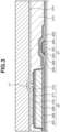
- Fig. 3 is a sectional view along the line A-A' of Fig. 2 .
- the photoelectric conversion element 20 is disposed on the left, and the TFT 21 is disposed on the right.
- the TFT 21 includes a gate electrode 301, a source electrode 302, a drain electrode 303, an insulation layer 304, a first semiconductor layer 305, and a first impurity semiconductor layer 306.
- the photoelectric conversion element 20 includes an individual electrode 307, a second impurity semiconductor layer 308, a second semiconductor layer 309, a third impurity semiconductor layer 310, a common electrode 311, and a protection layer 312.
- the drain electrode 303 is connected to the individual electrode 307 by contact.
- the common electrode 311 is connected to the bias line 17 by contact.
- the gate electrode 301 of the TFT 21 serves as one portion of the first drive line 16a, and the source electrode 302 serves as one portion of the signal line 15.
- the TFT 21 is turned on by the first drive line 16a, so that an electric charge of the photoelectric conversion element 20 is transferred as an electric signal to the signal line 15.
- a light shielding layer including metal may be arranged above the TFT 21 to reduce influence of light to be emitted to the TFT 21.
- a light shielding layer may include a metal layer that is the same as that of the bias line 17. In such a case, the light shielding layer and the bias line 17 can be connected.
- a circuit arrangement of a radiation imaging apparatus 100 according to the second embodiment is similar to that of the first embodiment illustrated in Fig. 1 .
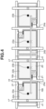
- Fig. 4 is a plan view illustrating pixels 1 according to the present embodiment.
- the present embodiment differs from the first embodiment in including an elimination portion 41 in a photoelectric conversion element 20.
- the photoelectric conversion element 20 has the elimination portion 41 in which a photoelectric conversion layer is eliminated.
- the elimination portion 41 is arranged on the side opposite a signal line 15 with a gravity center 23a therebetween, so that a gravity center of an aperture portion 22a/22b is provided nearer to the signal line 15.
- a distance between gravity centers is adjusted, so that a first gravity-center-to-gravity-center distance 24a and a second gravity-center-to-gravity-center distance 24b can match each other.
- the present embodiment has been described using a gravity center and a gravity-center-to-gravity-center distance, as similar to the first embodiment. However, the similar phenomenon occurs even in a case where a center and a center-to-center distance are used.
- Fig. 5 is an equivalent circuit diagram illustrating circuit arrangement of a radiation imaging apparatus 100 according to the present embodiment.
- the radiation imaging apparatus 100 of the present embodiment differs from that of the first embodiment in that four pixels sequentially arranged in a row direction are connected to one signal line 15. That is, a first pixel 1a, a second pixel 1b, a third pixel 1c, and a fourth pixel 1d are connected to one signal line 15.
- first pixel 1a, the second pixel 1b, the third pixel 1c, and the fourth pixel 1d are respectively connected to a first drive line 16a, a second drive line 16b, a third drive line 16c, and a fourth drive line 16d.
- each of the pixels 1a, 1b, 1c, and 1d is connected to a bias line 17.
- a pixel set 2 includes the four pixels of the first pixel 1a, the second pixel 1b, the third pixel 1c, and the fourth pixel 1d, and is repeatedly arranged in a periodic manner in a row direction. That is, a first pixel set includes the first pixel 1a, the second pixel 1b, the third pixel 1c, and the fourth pixel 1d which are sequentially arranged, and a second pixel set includes four pixels that are sequentially arranged from the right of the fourth pixel 1d. Shapes of aperture portions 22a/22b in a pixel set differ from one another, as similar to the description with reference to Fig. 2 .
- moire can be simplified by the similar method.
- the present embodiment has been described using a gravity center and a gravity-center-to-gravity-center distance, as similar to the first embodiment. However, the similar phenomenon occurs even in a case where a center and a center-to-center distance are used.
- moire can be simplified by the similar method. That is, in a case where a pixel set 2 in which a plurality of pixels is adjacent in a certain direction is repeatedly arranged in a periodic manner in a direction in which the pixels of the pixel set 2 are adjacent, moire can be simplified by the method according to the present embodiment.
- a circuit arrangement of a radiation imaging apparatus 100 according to the fourth embodiment is similar to that of the first embodiment illustrated in Fig. 1 .
- Fig. 6 is a plan view illustrating pixels 1 according to the fourth embodiment.
- a shape of a bias line 17 differs from that of the first embodiment.
- An aperture portion 22a of a first pixel 1a in the present embodiment has a shape that is substantially point-symmetrical with respect to a gravity center 23a of the aperture portion 22a of the first pixel 1a. In radiographic imaging using grids, such a substantially point-symmetrical shape enables moire to be simplified with respect to any direction.
- the present embodiment has been described using a gravity center and a gravity-center-to-gravity-center distance, as similar to the first embodiment. However, the similar phenomenon occurs even in a case where a center and a center-to-center distance are used.
- An X-ray 6060 generated by an X-ray tube 6050 that is a radiation source is transmitted to a chest 6062 of a patient or a subject 6061, and then enters into a radiation imaging apparatus 6040 typified by the above-described radiation imaging apparatus 100.
- the X-ray 6060 which has entered into the radiation imaging apparatus 6040 contains information about an internal body of the subject 6061.
- a scintillator emits light in response to the incidence of the X-ray, and the light is photoelectrically converted by a photoelectric conversion element to acquire electrical information. Such information is digitally converted, and the resultant digital information is processed as a radiation image by an image processor 6070 that is a signal processing unit. Then, the radiation image can be observed on a display 6080 that is a display unit in a control room.
- such information can be transferred to a remote location by a transmission processing unit such as a telephone line 6090.
- a transmission processing unit such as a telephone line 6090.
- the information can be displayed on a display 6081 that is a display unit in a doctor room of another location, or can be stored in a recording unit such as an optical disk, so that a physician in a remote location can make a diagnosis.
- the information can be recorded in a film 6110 that is a recoding medium by a film processor 6100 that is a recording unit.
Landscapes
- Physics & Mathematics (AREA)
- Health & Medical Sciences (AREA)
- Life Sciences & Earth Sciences (AREA)
- General Physics & Mathematics (AREA)
- High Energy & Nuclear Physics (AREA)
- Molecular Biology (AREA)
- Spectroscopy & Molecular Physics (AREA)
- Engineering & Computer Science (AREA)
- Multimedia (AREA)
- Signal Processing (AREA)
- Measurement Of Radiation (AREA)
- Solid State Image Pick-Up Elements (AREA)
- Transforming Light Signals Into Electric Signals (AREA)
- Thin Film Transistor (AREA)
- Apparatus For Radiation Diagnosis (AREA)
Abstract
Description
- The present disclosure relates to a radiation imaging apparatus and a radiation imaging system.
- Radiation imaging apparatuses each including pixels arranged in a two-dimensional matrix and using a flat panel detector (FPD) connected to a drive circuit and a readout circuit are widely used. The pixel includes a photoelectric conversion element and a switch element. The drive circuit and the readout circuit are used to drive a pixel to read out a signal.
- An integrated circuit (IC) chip to be used in the readout circuit is costly since an analog amplifier and an analog-to-digital (A/D) converter are integrated at a high density. A proportion of the IC chip cost in component cost of the radiation imaging apparatus is high.
-
Japanese Patent Application Laid-Open No. 2021-78050 - In the radiation imaging apparatus discussed in
Japanese Patent Application Laid-Open No. 2021-78050 - In a case where an image is captured using grids with respect to such a radiation imaging apparatus, complex moire occurs in the captured image due to a period in which gravity centers or centers of pixel apertures are equally spaced apart on an every-other-pixel basis. An increase in complexity of moire hinders removal of the moire by image processing. Consequently, image quality may be degraded.
- According to a first aspect of the present invention, there is provided a radiation imaging apparatus as specified in claims 1 to 11. According to a second aspect of the present invention, there is provided a radiation imaging system as specified in
claim 12. - Further features of the present disclosure will become apparent from the following description of embodiments with reference to the attached drawings.
-
-
Fig. 1 is an equivalent circuit diagram illustrating circuit arrangement of a radiation imaging apparatus according to a first embodiment. -
Fig. 2 is a plan view illustrating pixels according to the first embodiment. -
Fig. 3 is a sectional view illustrating the pixel according to the first embodiment. -
Fig. 4 is a plan view illustrating pixels according to a second embodiment. -
Fig. 5 is an equivalent circuit diagram illustrating circuit arrangement of a radiation imaging apparatus according to a third embodiment. -
Fig. 6 is a plan view illustrating pixels according to a fourth embodiment. -
Fig. 7 is a diagram illustrating a configuration example of a radiation imaging system according to a fifth embodiment. - Embodiments of the present disclosure are described with reference to the drawings. In the present specification, radiation includes an α-ray, a β-ray, and a γ-ray each of which is a beam created by a particle (including a photon) released by radioactive decay. The radiation also includes a beam, for example, an X-ray, a particle ray, and a cosmic ray. Such a beam has an energy substantially greater than or equal to that of the beam created by a particle released by radioactive decay. Each of the embodiments of the present invention described below can be implemented solely or as a combination of a plurality of the embodiments or features thereof where necessary or where the combination of elements or features from individual embodiments in a single embodiment is beneficial.
-
Fig. 1 is an equivalent circuit diagram illustrating circuit arrangement of aradiation imaging apparatus 100 according to a first embodiment of the present disclosure. Theradiation imaging apparatus 100 in the present embodiment includes apixel unit 10 in which a plurality of pixels 1 is arranged in a matrix on a substrate, areadout circuit 11, aninformation processing circuit 12 which includes an information processing circuit memory and an arithmetic processing unit, agate drive circuit 13, and apower supply circuit 14. - In
Fig. 1 , the pixels 1 in thepixel unit 10 are arranged in a 4 × 6 matrix for the sake of description. However, the arrangement is not limited thereto. Practically, more pixels 1 are arranged in thepixel unit 10. For example, approximately 3000 pixels 1 are arranged in each row and each column in thepixel unit 10. Apixel set 2 includes two adjacent pixels. InFig. 1 , thepixel set 2 includes afirst pixel 1a and asecond pixel 1b. Moreover, thepixel set 2 is repeatedly arranged in a periodic manner in a direction in which thefirst pixel 1a and thesecond pixel 1b are adjacent to each other. - A
signal line 15 is wiring to read out a signal acquired by the pixel 1 to thereadout circuit 11. As illustrated inFig. 1 , two pixels 1 adjacent to each other, that is, thefirst pixel 1a and thesecond pixel 1b, are connected to onesignal line 15. - A drive line 16 is wiring to supply a signal to turn on a switch element included in the pixel 1. The
first pixel 1a and thesecond pixel 1b are connected to separate drive lines 16. That is, thefirst pixel 1a is connect to afirst drive line 16a, whereas thesecond pixel 1b is connected to asecond drive line 16b. Abias line 17 is wiring to supply a bias voltage to each pixel 1 of thepixel unit 10. -
Fig. 2 is a plan view illustrating the pixels 1 according to the first embodiment. InFig. 2 , a first pixel set and a second pixel set that are adjacently arranged in a row direction in thepixel unit 10 is illustrated. That is, four pixels are illustrated inFig. 2 . A scintillator that converts radiation into light is disposed above the pixel 1 although the scintillator is omitted inFig. 2 . The light converted by the scintillator is converted into an electric charge by aphotoelectric conversion element 20, and the electric charge is transferred as an electric signal to thesignal line 15 via the switch element. - The pixel 1 includes the
photoelectric conversion element 20 and a thin film transistor (TFT) 21 that is used as a switch element. In addition, various kinds of wiring, such as thesignal line 15, the drive line 16, and thebias line 17, is arranged on the pixel 1 to drive the pixel 1 and read out a signal. - The signal from the
photoelectric conversion element 20 is transferred to thesignal line 15 via theTFT 21. Thefirst drive line 16a and thesecond drive line 16b control ON/OFF of theTFT 21. Thebias line 17 is connected to an upper electrode of thephotoelectric conversion element 20. - The
photoelectric conversion element 20 includes a light shield portion in which light is shielded by thebias line 17. - Accordingly, as for a shape of an aperture portion (a shaded area in
Fig. 2 ) that can receive light, a shape of anaperture portion 22a of thefirst pixel 1a differs from a shape of anaperture portion 22b of thesecond pixel 1b. Herein, theaperture portion 22a of thefirst pixel 1a has agravity center 23a, and theaperture portion 22b of thesecond pixel 1b has agravity center 23b. In this case, a first gravity-center-to-gravity-center distance 24a and a second gravity-center-to-gravity-center distance 24b are provided. The first gravity-center-to-gravity-center distance 24a is a distance between gravity centers of adjacent pixels with thesignal line 15 arranged between the adjacent pixels, whereas the second gravity-center-to-gravity-center distance 24b is a distance between gravity centers of adjacent pixels without thesignal line 15 arranged between the adjacent pixels. - In the present embodiment, the first gravity-center-to-gravity-
center distance 24a and the second gravity-center-to-gravity-center distance 24b are substantially the same. TheTFT 21 connected to thefirst pixel 1a is disposed on the side of thesignal line 15 relative to thegravity center 23a. The arrangement of theTFT 21 on the side of thesignal line 15 reduces an area of theaperture portion 22a/22b by an area for the arrangement of theTFT 21. This causes the gravity center of theaperture portion 22a/22b to be farther from thesignal line 15. - Accordingly, the light shield portion in which light on the
aperture portion 22a/22b is shielded by thebias line 17 is arranged on the side opposite thesignal line 15 with thegravity center 23a therebetween, so that the gravity center of theaperture portion 22a/22b is provided nearer to thesignal line 15. Accordingly, a distance between the gravity centers is adjusted, and thus the first gravity-center-to-gravity-center distance 24a and the second gravity-center-to-gravity-center distance 24b can match each other. - Regarding the situation in which the first gravity-center-to-gravity-
center distance 24a and the second gravity-center-to-gravity-center distance 24b are substantially the same, the first gravity-center-to-gravity-center distance 24a and the second gravity-center-to-gravity-center distance 24b are desirably within 5% from an average value of the first gravity-center-to-gravity-center distance 24a and the second gravity-center-to-gravity-center distance 24b, and more desirably within 2% from an average value of the first gravity-center-to-gravity-center distance 24a and the second gravity-center-to-gravity-center distance 24b. - If a first gravity-center-to-gravity-
center distance 24a and a second gravity-center-to-gravity-center distance 24b are substantially the same, it can be considered that a period having a gravity center of a pixel with respect to a row direction is generally the first gravity-center-to-gravity-center distance 24a only. On the other hand, if a difference in values between a first gravity-center-to-gravity-center distance 24a and a second gravity-center-to-gravity-center distance 24b is greater, a long period that is addition of the first gravity-center-to-gravity-center distance 24a and the second gravity-center-to-gravity-center distance 24b may be generated as a period having a gravity center of a pixel with respect to a row direction. - In pixel arrangement by which such a long period is generated, consider a case where radiographic imaging using grids is performed. In this case, complex moire in which two types of moire overlap one another occurs. The two types of moire are influenced by an average period of the first gravity-center-to-gravity-
center distance 24a and the second gravity-center-to-gravity-center distance 24b and a long period that is addition of the first gravity-center-to-gravity-center distance 24a and the second gravity-center-to-gravity-center distance 24b. - In a case where complex moire occurs, image processing is difficult. Consequently, image quality may be degraded.
- According to the present embodiment, on the other hand, in pixel arrangement in which a first gravity-center-to-gravity-
center distance 24a and a second gravity-center-to-gravity-center distance 24b are substantially the same, moire due to only the first gravity-center-to-gravity-center distance 24a occurs. Thus, the moire is simpler. The simpler the moire, the easier the image processing. Hence, image quality can be enhanced. - The gravity center in the present disclosure is determined by dividing an aperture portion into segments each having an optional shape, and then dividing a total sum of addition of position moments and areas of the segments by a total sum of the areas.
- In addition, if centers of aperture portions are the same, the similar effects are provided. The term "center" used in the present disclosure represents a position in which an aperture portion is divided into four equal parts by two lines not only passing through the center but also parallel to a row and a column. The present embodiment has been described using a gravity center and a gravity-center-to-gravity-center distance. However, the similar phenomenon occurs even in a case where a center and a center-to-center distance are used.
-
Fig. 3 is a sectional view along the line A-A' ofFig. 2 . Thephotoelectric conversion element 20 is disposed on the left, and theTFT 21 is disposed on the right. TheTFT 21 includes agate electrode 301, asource electrode 302, adrain electrode 303, aninsulation layer 304, afirst semiconductor layer 305, and a firstimpurity semiconductor layer 306. - The
photoelectric conversion element 20 includes anindividual electrode 307, a secondimpurity semiconductor layer 308, asecond semiconductor layer 309, a thirdimpurity semiconductor layer 310, acommon electrode 311, and aprotection layer 312. - The
drain electrode 303 is connected to theindividual electrode 307 by contact. Thecommon electrode 311 is connected to thebias line 17 by contact. Thegate electrode 301 of theTFT 21 serves as one portion of thefirst drive line 16a, and thesource electrode 302 serves as one portion of thesignal line 15. TheTFT 21 is turned on by thefirst drive line 16a, so that an electric charge of thephotoelectric conversion element 20 is transferred as an electric signal to thesignal line 15. - A light shielding layer including metal may be arranged above the
TFT 21 to reduce influence of light to be emitted to theTFT 21. A light shielding layer may include a metal layer that is the same as that of thebias line 17. In such a case, the light shielding layer and thebias line 17 can be connected. - Next, a second embodiment of the present disclosure is described. In the second embodiment, redundant descriptions of the first embodiment are omitted.
- A circuit arrangement of a
radiation imaging apparatus 100 according to the second embodiment is similar to that of the first embodiment illustrated inFig. 1 . -
Fig. 4 is a plan view illustrating pixels 1 according to the present embodiment. The present embodiment differs from the first embodiment in including anelimination portion 41 in aphotoelectric conversion element 20. Thephotoelectric conversion element 20 has theelimination portion 41 in which a photoelectric conversion layer is eliminated. - Similar to the light shield portion described in the first embodiment, the
elimination portion 41 is arranged on the side opposite asignal line 15 with agravity center 23a therebetween, so that a gravity center of anaperture portion 22a/22b is provided nearer to thesignal line 15. - Accordingly, a distance between gravity centers is adjusted, so that a first gravity-center-to-gravity-
center distance 24a and a second gravity-center-to-gravity-center distance 24b can match each other. - As a result, in the present embodiment, moire that occurs in radiographic imaging using grids is simplified, as similar to the first embodiment.
- The present embodiment has been described using a gravity center and a gravity-center-to-gravity-center distance, as similar to the first embodiment. However, the similar phenomenon occurs even in a case where a center and a center-to-center distance are used.
- Next, a third embodiment of the present disclosure is described. In the third embodiment, redundant descriptions of the first embodiment are omitted.
-
Fig. 5 is an equivalent circuit diagram illustrating circuit arrangement of aradiation imaging apparatus 100 according to the present embodiment. Theradiation imaging apparatus 100 of the present embodiment differs from that of the first embodiment in that four pixels sequentially arranged in a row direction are connected to onesignal line 15. That is, afirst pixel 1a, asecond pixel 1b, athird pixel 1c, and afourth pixel 1d are connected to onesignal line 15. - These four pixels are connected to different drive lines 16. That is, the
first pixel 1a, thesecond pixel 1b, thethird pixel 1c, and thefourth pixel 1d are respectively connected to afirst drive line 16a, asecond drive line 16b, athird drive line 16c, and afourth drive line 16d. In addition, each of thepixels bias line 17. - A pixel set 2 includes the four pixels of the
first pixel 1a, thesecond pixel 1b, thethird pixel 1c, and thefourth pixel 1d, and is repeatedly arranged in a periodic manner in a row direction. That is, a first pixel set includes thefirst pixel 1a, thesecond pixel 1b, thethird pixel 1c, and thefourth pixel 1d which are sequentially arranged, and a second pixel set includes four pixels that are sequentially arranged from the right of thefourth pixel 1d. Shapes ofaperture portions 22a/22b in a pixel set differ from one another, as similar to the description with reference toFig. 2 . Even in a case where such four adjacent pixels in a row direction are connected to one signal line, a shape of a light shield portion or an elimination portion is adjusted, so that each of gravity-center-to-gravity-center distances of the pixels is matched. Thus, moire that occurs in radiographic imaging using grids can be simplified. - In addition, even in a case where a number of pixels in a pixel set 2 is other than two or four, moire can be simplified by the similar method. The present embodiment has been described using a gravity center and a gravity-center-to-gravity-center distance, as similar to the first embodiment. However, the similar phenomenon occurs even in a case where a center and a center-to-center distance are used.
- In addition, even in a case where a pixel set 2 includes pixels that are adjacently arranged in a column direction, moire can be simplified by the similar method. That is, in a case where a pixel set 2 in which a plurality of pixels is adjacent in a certain direction is repeatedly arranged in a periodic manner in a direction in which the pixels of the pixel set 2 are adjacent, moire can be simplified by the method according to the present embodiment.
- Next, a fourth embodiment of the present disclosure is described. In the fourth embodiment, redundant descriptions of the first embodiment are omitted.
- A circuit arrangement of a
radiation imaging apparatus 100 according to the fourth embodiment is similar to that of the first embodiment illustrated inFig. 1 . -
Fig. 6 is a plan view illustrating pixels 1 according to the fourth embodiment. In the present embodiment, a shape of abias line 17 differs from that of the first embodiment. Anaperture portion 22a of afirst pixel 1a in the present embodiment has a shape that is substantially point-symmetrical with respect to agravity center 23a of theaperture portion 22a of thefirst pixel 1a. In radiographic imaging using grids, such a substantially point-symmetrical shape enables moire to be simplified with respect to any direction. - The present embodiment has been described using a gravity center and a gravity-center-to-gravity-center distance, as similar to the first embodiment. However, the similar phenomenon occurs even in a case where a center and a center-to-center distance are used.
- Hereinafter, an example in which the
radiation imaging apparatus 100 of any of the above embodiments is applied to a radiation imaging system is described with reference toFig. 7 . AnX-ray 6060 generated by anX-ray tube 6050 that is a radiation source is transmitted to achest 6062 of a patient or a subject 6061, and then enters into a radiation imaging apparatus 6040 typified by the above-describedradiation imaging apparatus 100. TheX-ray 6060 which has entered into the radiation imaging apparatus 6040 contains information about an internal body of the subject 6061. - A scintillator emits light in response to the incidence of the X-ray, and the light is photoelectrically converted by a photoelectric conversion element to acquire electrical information. Such information is digitally converted, and the resultant digital information is processed as a radiation image by an
image processor 6070 that is a signal processing unit. Then, the radiation image can be observed on adisplay 6080 that is a display unit in a control room. - In addition, such information can be transferred to a remote location by a transmission processing unit such as a
telephone line 6090. Thus, the information can be displayed on adisplay 6081 that is a display unit in a doctor room of another location, or can be stored in a recording unit such as an optical disk, so that a physician in a remote location can make a diagnosis. Moreover, the information can be recorded in afilm 6110 that is a recoding medium by afilm processor 6100 that is a recording unit. - While the present invention has been described with reference to embodiments, it is to be understood that the invention is not limited to the disclosed embodiments. The scope of the following claims is to be accorded the broadest interpretation so as to encompass all such modifications and equivalent structures and functions.
Claims (12)
- A radiation imaging apparatus (100) comprising:a pixel unit (10) in which a plurality of pixels (1a, 1b; 1a, 1b, 1c, 1d) each including a photoelectric conversion element (20) configured to convert light into an electric charge and a switch element (21) is arranged in a matrix,wherein the pixel unit (10) includes a plurality of pixel sets (2) that are adjacently arranged in a predetermined direction, each of the plurality of pixel sets (2) including two or more of the pixels (1a, 1b; 1a, 1b, 1c, 1d), which are adjacently arranged in the predetermined direction and in which the photoelectric conversion elements (20) have aperture portions (22a, 22b) having different shapes, andwherein each of the aperture portions (22a, 22b) has a gravity center (23a, 23b) or center, and a distance (24a) between each of the gravity centers (23a, 23b) or the centers for adjacent pixels in the plurality of pixels are substantially the same.
- The radiation imaging apparatus (100) according to claim 1,wherein the plurality of pixel sets (2) include:a first pixel set (2) including a first pixel (1a) and a second pixel (1b) adjacent to the first pixel (1a) in the predetermined direction; anda second pixel set (2) including a third pixel adjacent to the second pixel in the predetermined direction and a fourth pixel adjacent to the third pixel in the predetermined direction, andwherein, in the pixel unit (10), the first pixel, the second pixel, the third pixel, and the fourth pixel are arranged such that a first distance, a second distance, and a third distance are substantially the same, the first distance (24a) being a distance between a gravity center (23a) or a center of the aperture portion (22a) the first pixel (1a) and a gravity center (23b) or a center of the aperture portion (22b) of the second pixel (1b), the second distance (24b) being a distance between the gravity center (23b) or the center of the aperture portion (22b) of the second pixel (1b) and a gravity center (23a) or a center of the aperture portion of the third pixel, and the third distance (24a) being a distance between the gravity center (23a) or the center of the aperture portion of the third pixel and a gravity center (23b) or a center of the aperture portion of the fourth pixel.
- The radiation imaging apparatus (100) according to claim 2, wherein the first distance (24a), the second distance (24b), and the third distance (24a) are within 5% from an average value of the first distance, the second distance, and the third distance.
- The radiation imaging apparatus (100) according to claim 2, further comprising:a signal line (15) configured to read out a signal acquired by the photoelectric conversion element (20); anda drive line (16a, 16b; 16a, 16b, 16c, 16d) configured to supply a signal to turn on the switch element (21),wherein the first pixel set (2) in the plurality of pixel sets (2) and the second pixel set (2) which is in the plurality of pixel sets (2) and adjacent to the first pixel set in the predetermined direction are connected to a common signal line (15) or drive lines (16a, 16b; 16a, 16b, 16c, 16d).
- The radiation imaging apparatus according to claim 4, comprising a light shield portion arranged on the aperture portion (22a, 22b) and configured to shield one portion of the photoelectric conversion element (20) from light.
- The radiation imaging apparatus (100) according to claim 5, wherein the light shield portion is arranged opposite the signal line (15) arranged on the aperture portion (22a, 22b) with the gravity center (23a, 23b) of the aperture portion (22a, 22b) between the light shield portion and the signal line (15).
- The radiation imaging apparatus (100) according to claim 5 or 6, wherein the light shield portion is a bias line (17) configured to supply to a bias voltage to each of the plurality of pixels (1a, 1b; 1a, 1b, 1c, 1d).
- The radiation imaging apparatus according to any one of claims 4 to 7, comprising an elimination portion (41) where one portion of the photoelectric conversion element (20) is eliminated.
- The radiation imaging apparatus according to claim 8, wherein the elimination portion (41) is arranged opposite the signal line (15) arranged on the aperture portion (22a, 22b) with the gravity center (23a, 23b) of the aperture portion (22a, 22b) between the elimination portion (41) and the signal line (15).
- A radiation imaging apparatus (100) comprising:a pixel unit (10) in which a plurality of pixels (1a, 1b; 1a, 1b, 1c, 1d) each including a photoelectric conversion element (20) configured to convert light into an electric charge and a switch element (21) is arranged in a matrix;a light shield portion (17) arranged on an aperture portion (22a, 22b) of the photoelectric conversion elements (20) of each pixel and configured to shield one portion of the photoelectric conversion elements (20) of each pixel from light; anda signal line (15) configured to read out a signal acquired by the photoelectric conversion elements (20) of each pixel,wherein the pixel unit (10) includes a first pixel set (2) and a second pixel set (2) that are adjacently arranged in a predetermined direction, each of the first pixel set (2) and the second pixel set (2) including two or more of the pixels (1a, 1b; 1a, 1b, 1c, 1d), which are adjacently arranged in the predetermined direction and in which the photoelectric conversion elements (20) of each pixel have aperture portions (22a, 22b) having different shapes, andwherein the light shield portion (17) is arranged opposite the signal line (15) arranged on the aperture portion (22a, 22b) with a gravity center (23a, 23b) of the aperture portion (22a, 22b) between the light shield portion (17) and the signal line (15).
- A radiation imaging apparatus comprising:a pixel unit (10) in which a plurality of pixels (1a, 1b; 1a, 1b, 1c, 1d) each including a photoelectric conversion element (20) configured to convert light into an electric charge and a switch element (21) is arranged in a matrix;an elimination portion (41) where one portion of the photoelectric conversion element (20) is eliminated; anda signal line (15) configured to read out a signal acquired by the photoelectric conversion element (20),wherein the pixel unit (10) includes a first pixel set (2) and a second pixel set (2) that are adjacently arranged in a predetermined direction, each of the first pixel set and the second pixel set including two or more of the pixels (1a, 1b; 1a, 1b, 1c, 1d), which are adjacently arranged in the predetermined direction and in which the photoelectric conversion elements (20) of each pixel have aperture portions (22a, 22b) having different shapes, andwherein the elimination portion (41) is arranged opposite the signal line (15) arranged on the aperture portion (22a, 22b) with a gravity center (23a, 23b) of the aperture portion (22a, 22b) between the elimination portion (41) and the signal line (15).
- A radiation imaging system comprising:the radiation imaging apparatus (100, 6040) according to any one of claims 1 to 11; andsignal processing means (6070) for processing a signal detected by the radiation imaging apparatus as a radiation image.
Applications Claiming Priority (1)
| Application Number | Priority Date | Filing Date | Title |
|---|---|---|---|
| JP2022056593A JP2023148519A (en) | 2022-03-30 | 2022-03-30 | Radiation imaging devices and radiation imaging systems |
Publications (1)
| Publication Number | Publication Date |
|---|---|
| EP4283679A1 true EP4283679A1 (en) | 2023-11-29 |
Family
ID=85726463
Family Applications (1)
| Application Number | Title | Priority Date | Filing Date |
|---|---|---|---|
| EP23163860.2A Withdrawn EP4283679A1 (en) | 2022-03-30 | 2023-03-23 | Radiation imaging apparatus and radiation imaging system |
Country Status (4)
| Country | Link |
|---|---|
| US (2) | US12339409B2 (en) |
| EP (1) | EP4283679A1 (en) |
| JP (1) | JP2023148519A (en) |
| CN (1) | CN116896676A (en) |
Citations (3)
| Publication number | Priority date | Publication date | Assignee | Title |
|---|---|---|---|---|
| EP0984316A2 (en) * | 1998-09-01 | 2000-03-08 | Canon Kabushiki Kaisha | Semiconductor apparatus and method for producing it |
| EP3823268A1 (en) * | 2019-11-12 | 2021-05-19 | Canon Kabushiki Kaisha | Radiation imaging apparatus and radiation imaging system |
| JP2021078050A (en) | 2019-11-12 | 2021-05-20 | キヤノン株式会社 | Radiation imaging device and radiation imaging system |
Family Cites Families (5)
| Publication number | Priority date | Publication date | Assignee | Title |
|---|---|---|---|---|
| JP3854720B2 (en) * | 1998-05-20 | 2006-12-06 | キヤノン株式会社 | Imaging apparatus and imaging system using the same |
| JP5092306B2 (en) * | 2006-08-02 | 2012-12-05 | ソニー株式会社 | Display device and pixel circuit layout method |
| JP2010271049A (en) * | 2009-05-19 | 2010-12-02 | Sony Corp | Two-dimensional solid-state imaging device |
| JP7288427B2 (en) * | 2017-07-11 | 2023-06-07 | コーニング インコーポレイテッド | Tiled display and manufacturing method thereof |
| JP7398931B2 (en) * | 2019-11-12 | 2023-12-15 | キヤノン株式会社 | Radiation imaging devices and radiation imaging systems |
-
2022
- 2022-03-30 JP JP2022056593A patent/JP2023148519A/en active Pending
-
2023
- 2023-03-21 CN CN202310282561.4A patent/CN116896676A/en active Pending
- 2023-03-23 EP EP23163860.2A patent/EP4283679A1/en not_active Withdrawn
- 2023-03-24 US US18/189,880 patent/US12339409B2/en active Active
-
2025
- 2025-05-29 US US19/222,239 patent/US20250291075A1/en active Pending
Patent Citations (3)
| Publication number | Priority date | Publication date | Assignee | Title |
|---|---|---|---|---|
| EP0984316A2 (en) * | 1998-09-01 | 2000-03-08 | Canon Kabushiki Kaisha | Semiconductor apparatus and method for producing it |
| EP3823268A1 (en) * | 2019-11-12 | 2021-05-19 | Canon Kabushiki Kaisha | Radiation imaging apparatus and radiation imaging system |
| JP2021078050A (en) | 2019-11-12 | 2021-05-20 | キヤノン株式会社 | Radiation imaging device and radiation imaging system |
Also Published As
| Publication number | Publication date |
|---|---|
| US12339409B2 (en) | 2025-06-24 |
| JP2023148519A (en) | 2023-10-13 |
| US20250291075A1 (en) | 2025-09-18 |
| CN116896676A (en) | 2023-10-17 |
| US20230314637A1 (en) | 2023-10-05 |
Similar Documents
| Publication | Publication Date | Title |
|---|---|---|
| KR100665144B1 (en) | Radiation detector and radiation image pickup device | |
| US7952077B2 (en) | Image sensor, image-sensing apparatus using the image sensor, and image-sensing system | |
| JP5162085B2 (en) | Solid X-ray detector with improved spatial resolution | |
| EP3298772B1 (en) | Radiation imaging apparatus and radiation imaging system | |
| US9887224B2 (en) | Detection apparatus having covering layer disposed on interlayer insulating layer in a pixel-array outside region, and detection system including detection apparatus | |
| US10236091B2 (en) | Backscatter shields and methods of shielding | |
| US10921466B2 (en) | Radiation imaging apparatus and radiation imaging system | |
| JP2019141357A (en) | Radiographic apparatus and radiographic system | |
| US7429723B2 (en) | Conversion apparatus, radiation detection apparatus, and radiation detection system | |
| JPS62167535A (en) | radiography equipment | |
| US20250291072A1 (en) | Radiation imaging apparatus and radiation imaging system | |
| JP2020065727A (en) | Radiation imaging apparatus, radiation imaging method and program | |
| US20030235273A1 (en) | X-ray diagnostic facility having a digital X-ray detector and a stray radiation grid | |
| EP4283679A1 (en) | Radiation imaging apparatus and radiation imaging system | |
| JP6719324B2 (en) | Radiation imaging apparatus and radiation imaging system | |
| JP2018195949A (en) | Radiation imaging device and radiation imaging system | |
| US12265188B2 (en) | Apparatus and system | |
| JP6929327B2 (en) | Radiation imaging device and radiation imaging system | |
| JP2023175411A (en) | Radiographic device and radiographic system | |
| JP2023119569A (en) | Radiation imaging apparatus and radiation imaging system | |
| CN116602693A (en) | Radiation imaging apparatus and radiation imaging system |
Legal Events
| Date | Code | Title | Description |
|---|---|---|---|
| PUAI | Public reference made under article 153(3) epc to a published international application that has entered the european phase |
Free format text: ORIGINAL CODE: 0009012 |
|
| STAA | Information on the status of an ep patent application or granted ep patent |
Free format text: STATUS: THE APPLICATION HAS BEEN PUBLISHED |
|
| AK | Designated contracting states |
Kind code of ref document: A1 Designated state(s): AL AT BE BG CH CY CZ DE DK EE ES FI FR GB GR HR HU IE IS IT LI LT LU LV MC ME MK MT NL NO PL PT RO RS SE SI SK SM TR |
|
| STAA | Information on the status of an ep patent application or granted ep patent |
Free format text: STATUS: REQUEST FOR EXAMINATION WAS MADE |
|
| 17P | Request for examination filed |
Effective date: 20240529 |
|
| RBV | Designated contracting states (corrected) |
Designated state(s): AL AT BE BG CH CY CZ DE DK EE ES FI FR GB GR HR HU IE IS IT LI LT LU LV MC ME MK MT NL NO PL PT RO RS SE SI SK SM TR |
|
| STAA | Information on the status of an ep patent application or granted ep patent |
Free format text: STATUS: EXAMINATION IS IN PROGRESS |
|
| 17Q | First examination report despatched |
Effective date: 20240822 |
|
| STAA | Information on the status of an ep patent application or granted ep patent |
Free format text: STATUS: THE APPLICATION HAS BEEN WITHDRAWN |
|
| 18W | Application withdrawn |
Effective date: 20241010 |