EP4283664A1 - Wafer level chip scale package with sidewall protection - Google Patents
Wafer level chip scale package with sidewall protection Download PDFInfo
- Publication number
- EP4283664A1 EP4283664A1 EP23168683.3A EP23168683A EP4283664A1 EP 4283664 A1 EP4283664 A1 EP 4283664A1 EP 23168683 A EP23168683 A EP 23168683A EP 4283664 A1 EP4283664 A1 EP 4283664A1
- Authority
- EP
- European Patent Office
- Prior art keywords
- adhesive layer
- bare silicon
- silicon die
- wafer level
- chip scale
- Prior art date
- Legal status (The legal status is an assumption and is not a legal conclusion. Google has not performed a legal analysis and makes no representation as to the accuracy of the status listed.)
- Pending
Links
Images



Classifications
-
- H—ELECTRICITY
- H10—SEMICONDUCTOR DEVICES; ELECTRIC SOLID-STATE DEVICES NOT OTHERWISE PROVIDED FOR
- H10W—GENERIC PACKAGES, INTERCONNECTIONS, CONNECTORS OR OTHER CONSTRUCTIONAL DETAILS OF DEVICES COVERED BY CLASS H10
- H10W74/00—Encapsulations, e.g. protective coatings
- H10W74/10—Encapsulations, e.g. protective coatings characterised by their shape or disposition
- H10W74/111—Encapsulations, e.g. protective coatings characterised by their shape or disposition the semiconductor body being completely enclosed
- H10W74/129—Encapsulations, e.g. protective coatings characterised by their shape or disposition the semiconductor body being completely enclosed forming a chip-scale package [CSP]
-
- H—ELECTRICITY
- H10—SEMICONDUCTOR DEVICES; ELECTRIC SOLID-STATE DEVICES NOT OTHERWISE PROVIDED FOR
- H10W—GENERIC PACKAGES, INTERCONNECTIONS, CONNECTORS OR OTHER CONSTRUCTIONAL DETAILS OF DEVICES COVERED BY CLASS H10
- H10W74/00—Encapsulations, e.g. protective coatings
- H10W74/10—Encapsulations, e.g. protective coatings characterised by their shape or disposition
- H10W74/131—Encapsulations, e.g. protective coatings characterised by their shape or disposition the semiconductor body being only partially enclosed
- H10W74/141—Encapsulations, e.g. protective coatings characterised by their shape or disposition the semiconductor body being only partially enclosed the encapsulations being on at least the sidewalls of the semiconductor body
-
- H—ELECTRICITY
- H10—SEMICONDUCTOR DEVICES; ELECTRIC SOLID-STATE DEVICES NOT OTHERWISE PROVIDED FOR
- H10P—GENERIC PROCESSES OR APPARATUS FOR THE MANUFACTURE OR TREATMENT OF DEVICES COVERED BY CLASS H10
- H10P54/00—Cutting or separating of wafers, substrates or parts of devices
-
- H—ELECTRICITY
- H10—SEMICONDUCTOR DEVICES; ELECTRIC SOLID-STATE DEVICES NOT OTHERWISE PROVIDED FOR
- H10P—GENERIC PROCESSES OR APPARATUS FOR THE MANUFACTURE OR TREATMENT OF DEVICES COVERED BY CLASS H10
- H10P72/00—Handling or holding of wafers, substrates or devices during manufacture or treatment thereof
- H10P72/70—Handling or holding of wafers, substrates or devices during manufacture or treatment thereof for supporting or gripping
- H10P72/74—Handling or holding of wafers, substrates or devices during manufacture or treatment thereof for supporting or gripping using temporarily an auxiliary support
- H10P72/7402—Wafer tapes, e.g. grinding or dicing support tapes
-
- H—ELECTRICITY
- H10—SEMICONDUCTOR DEVICES; ELECTRIC SOLID-STATE DEVICES NOT OTHERWISE PROVIDED FOR
- H10W—GENERIC PACKAGES, INTERCONNECTIONS, CONNECTORS OR OTHER CONSTRUCTIONAL DETAILS OF DEVICES COVERED BY CLASS H10
- H10W42/00—Arrangements for protection of devices
- H10W42/121—Arrangements for protection of devices protecting against mechanical damage
-
- H—ELECTRICITY
- H10—SEMICONDUCTOR DEVICES; ELECTRIC SOLID-STATE DEVICES NOT OTHERWISE PROVIDED FOR
- H10W—GENERIC PACKAGES, INTERCONNECTIONS, CONNECTORS OR OTHER CONSTRUCTIONAL DETAILS OF DEVICES COVERED BY CLASS H10
- H10W74/00—Encapsulations, e.g. protective coatings
- H10W74/01—Manufacture or treatment
- H10W74/014—Manufacture or treatment using batch processing
-
- H—ELECTRICITY
- H10—SEMICONDUCTOR DEVICES; ELECTRIC SOLID-STATE DEVICES NOT OTHERWISE PROVIDED FOR
- H10W—GENERIC PACKAGES, INTERCONNECTIONS, CONNECTORS OR OTHER CONSTRUCTIONAL DETAILS OF DEVICES COVERED BY CLASS H10
- H10W74/00—Encapsulations, e.g. protective coatings
- H10W74/10—Encapsulations, e.g. protective coatings characterised by their shape or disposition
- H10W74/131—Encapsulations, e.g. protective coatings characterised by their shape or disposition the semiconductor body being only partially enclosed
- H10W74/137—Encapsulations, e.g. protective coatings characterised by their shape or disposition the semiconductor body being only partially enclosed the encapsulations being directly on the semiconductor body
-
- H—ELECTRICITY
- H10—SEMICONDUCTOR DEVICES; ELECTRIC SOLID-STATE DEVICES NOT OTHERWISE PROVIDED FOR
- H10P—GENERIC PROCESSES OR APPARATUS FOR THE MANUFACTURE OR TREATMENT OF DEVICES COVERED BY CLASS H10
- H10P72/00—Handling or holding of wafers, substrates or devices during manufacture or treatment thereof
- H10P72/70—Handling or holding of wafers, substrates or devices during manufacture or treatment thereof for supporting or gripping
- H10P72/74—Handling or holding of wafers, substrates or devices during manufacture or treatment thereof for supporting or gripping using temporarily an auxiliary support
- H10P72/7416—Handling or holding of wafers, substrates or devices during manufacture or treatment thereof for supporting or gripping using temporarily an auxiliary support used during dicing or grinding
-
- H—ELECTRICITY
- H10—SEMICONDUCTOR DEVICES; ELECTRIC SOLID-STATE DEVICES NOT OTHERWISE PROVIDED FOR
- H10P—GENERIC PROCESSES OR APPARATUS FOR THE MANUFACTURE OR TREATMENT OF DEVICES COVERED BY CLASS H10
- H10P72/00—Handling or holding of wafers, substrates or devices during manufacture or treatment thereof
- H10P72/70—Handling or holding of wafers, substrates or devices during manufacture or treatment thereof for supporting or gripping
- H10P72/74—Handling or holding of wafers, substrates or devices during manufacture or treatment thereof for supporting or gripping using temporarily an auxiliary support
- H10P72/7434—Handling or holding of wafers, substrates or devices during manufacture or treatment thereof for supporting or gripping using temporarily an auxiliary support used in a transfer process involving at least two transfer steps, i.e. including an intermediate handle substrate
-
- H—ELECTRICITY
- H10—SEMICONDUCTOR DEVICES; ELECTRIC SOLID-STATE DEVICES NOT OTHERWISE PROVIDED FOR
- H10P—GENERIC PROCESSES OR APPARATUS FOR THE MANUFACTURE OR TREATMENT OF DEVICES COVERED BY CLASS H10
- H10P72/00—Handling or holding of wafers, substrates or devices during manufacture or treatment thereof
- H10P72/70—Handling or holding of wafers, substrates or devices during manufacture or treatment thereof for supporting or gripping
- H10P72/74—Handling or holding of wafers, substrates or devices during manufacture or treatment thereof for supporting or gripping using temporarily an auxiliary support
- H10P72/7438—Handling or holding of wafers, substrates or devices during manufacture or treatment thereof for supporting or gripping using temporarily an auxiliary support with parts of the auxiliary support remaining in the finished device
-
- H—ELECTRICITY
- H10—SEMICONDUCTOR DEVICES; ELECTRIC SOLID-STATE DEVICES NOT OTHERWISE PROVIDED FOR
- H10W—GENERIC PACKAGES, INTERCONNECTIONS, CONNECTORS OR OTHER CONSTRUCTIONAL DETAILS OF DEVICES COVERED BY CLASS H10
- H10W72/00—Interconnections or connectors in packages
- H10W72/20—Bump connectors, e.g. solder bumps or copper pillars; Dummy bumps; Thermal bumps
Definitions
- the present disclosure relates generally to the field of semiconductor packaging. More particularly, the present disclosure relates to an improved wafer level chip scale package (WLCSP) with sidewall protection.
- WLCSP wafer level chip scale package
- a chip scale package has overall package dimensions substantially equal to that of the silicon active device or die that is enclosed within the package.
- One such type of CSP is manufactured in wafer form and hence referred to as a wafer level CSP or WLCSP.
- a surface mount die is a WLCSP in which I/O contacts are in bump form and located on the active side of the die.
- WLCSP devices may be subjected to a number of processes and stress which may affect product yield and product reliability. For example, after singulation, the backside corner of a bare silicon die is easily damaged with chipping during the transportation and physical handling. As applications demand smaller and thinner die in WLCSP, the risk of die handling defects rise due to the absence of die sidewall protection.
- a wafer level chip scale package (WLCSP) with sidewall protection in order to solve the above-mentioned prior art deficiencies or shortcomings.
- WLCSP wafer level chip scale package
- a wafer level chip scale package according to the invention is defined in independent claim 1.
- the dependent claims define preferred embodiments thereof.
- a wafer level chip scale package including a bare silicon die having an active surface, a rear surface opposite to the active surface, and a sidewall surface between the active surface and the rear surface.
- the bare silicon die includes a backside corner between the rear surface and the sidewall surface.
- a plurality of pads is disposed on the active surface.
- a plurality of conductive elements is disposed on the plurality of pads, respectively.
- a backside tape is adhered to the rear surface by using an adhesive layer. The adhesive layer and the backside tape protrude beyond the sidewall surfaces of the bare silicon die. The adhesive layer extends along the sidewall surface and wraps around the backside corner.
- the bare silicon die is not encapsulated by a molding compound.
- the plurality of pads comprises solder pads or bump pads.
- the plurality of conductive elements comprises solder balls, solder bumps, metal bumps, micro-bumps or metal pillars.
- the adhesive layer and the backside tape protrude beyond the sidewall surfaces of the bare silicon die by a distance of 5-40 micrometers.
- a height of the adhesive layer on the sidewall surfaces of the bare silicon die is equal to or less than 25 micrometers.
- the adhesive layer only partially covers the sidewall surface of the bare silicon die.
- an included angle between an end surface of the adhesive layer and the sidewall surface of the bare silicon die is a right angle.
- an included angle between an end surface of the adhesive layer and the sidewall surface of the bare silicon die is an acute angle.
- an included angle between an end surface of the adhesive layer and the sidewall surface of the bare silicon die is an obtuse angle.
- Handling defects such as, die corner stress, chipping and or die cracks can cause functional failures which may happen during the WLCSP processing or arise over the electronic product's life due to environment temperature or mechanic use stresses.
- WLCSP handling defects can occur at any step across the device process flow from WLCSP back end processes of dicing through tape and reel packing to the final surface mount of the WLCSP device on the product printed circuit board assembly (PCBA). After singulation, the backside corner of a bare silicon die is easily damaged with chipping during the transportation and physical handling. The present invention addresses this issue.
- FIG. 1 is a schematic top view of a wafer level chip scale package (WLCSP) 10 according to an embodiment of the invention.
- FIG. 2 is a bottom view of the WLCSP 10 in FIG. 1 .
- FIG. 3 is a schematic, cross-sectional view taken along line I-I' in FIG. 1 .
- the WLCSP 10 comprises a bare silicon die 100, which is not encapsulated by a molding compound.
- the bare silicon die 100 comprises an active surface S1 and a rear surface S2 opposite to the active surface S1 and four sidewall surfaces SW between the active surface S1 and the rear surface S2.
- a backside corner BC is defined between the rear surface S2 and the sidewall surface SW.
- a plurality of pads 101 such as solder pads or bump pads is provided on the active surface S1.
- a plurality of conductive elements 110 such as solder balls, solder bumps, metal bumps, micro-bumps or metal pillars may be disposed on the plurality of pads 101, respectively, for further connection.
- the plurality of pads 101 may be re-distributed pads formed in a re-distribution layer (RDL) structure (not shown).
- RDL re-distribution layer
- a backside tape 220 such as a polyethylene terephthalate (PET) tape
- PET polyethylene terephthalate
- an adhesive layer (or glue layer) 210 such as an epoxy resin layer.
- the adhesive layer 210 extends along the sidewall surfaces SW of the bare silicon die 100 and wraps around the backside corners BC.
- a height h of the adhesive layer 210 on the sidewall surfaces SW of the bare silicon die 100 may equal to or less than 25 micrometers.
- the rest portion of the sidewall surface SW is not covered by the adhesive layer 210.
- the adhesive layer 210 around the backside corners BC functions as a sidewall protection that can prevent sidewall damage or chipping during the transportation and physical handling.
- the included angle ⁇ between the end surface S3 of the adhesive layer 210 and the adjacent sidewall surface SW of the bare silicon die 100 may be approximately a right angle.
- the included angle ⁇ between the end surface S3 of the adhesive layer 210 and the adjacent sidewall surface SW of the bare silicon die 100 of the WLCSP 10a may be an acute angle.
- the included angle ⁇ between the end surface S3 of the adhesive layer 210 and the adjacent sidewall surface SW of the bare silicon die 100 of the WLCSP 10b may be an obtuse angle.
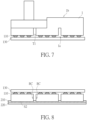
- FIG. 6 to FIG. 10 are schematic diagrams showing an exemplary method for fabricating a WLCSP with sidewall protection according to an embodiment of the invention, wherein like regions, elements or layers are designated by like numeral numbers or labels.
- a thin wafer 1 having a front side 1a and a back side 1b is provided.
- the thin wafer 1 comprises a plurality of die regions DA on the front side 1a.
- Integrated circuit elements are fabricated within each die region DA.
- a plurality of conductive elements 110 such as solder balls, solder bumps, or metal bumps are disposed on the die regions DA on the front side 1a.
- the plurality of die regions DA separated by dicing lanes SA.
- the front side 1a is subjected to a pre-cut process BL1 to form half-cut trenches T1 into the front side 1a of the thin wafer 1 along the dicing lanes SA.
- a grinding tape 130 is temporarily adhered to the front side 1a of the thin wafer 1.
- the thin wafer 1 is then subjected to a wafer backside grinding to remove a portion of the thin wafer 1 from its back side 1b, thereby forming individual bare silicon die 10.
- the die singulation occurs when the wafer 1 is thinned below the level of the half-cut trenches T1.
- a backside tape 220 is adhered to the rear surface S2 of the bare silicon die 10 through the adhesive layer 210.
- the adhesive layer 210 may be squeezed into the dicing lanes SA and may partially cover the sidewall surface SW of the bare silicon die 10 around the backside corner BC.
- the grinding tape 130 is removed, thereby forming a temporary structure TS.
- the active surface S1 and the conductive elements 110 on the active surface S1 are revealed.
- the temporary structure TS is then subjected to a sawing process BL2 to cut through the adhesive layer 210 and the backside tape 220 along the dicing lanes SA.
- the adhesive layer 210 extends along the sidewall surfaces SW of the bare silicon die 100 and wraps around the backside corners BC.
- a height h of the adhesive layer 210 on the sidewall surfaces SW of the bare silicon die 100 may equal to or less than 25 micrometers.
- the rest portion of the sidewall surface SW is not covered by the adhesive layer 210.
- the adhesive layer 210 around the backside corners BC functions as a sidewall protection that can prevent sidewall damage or chipping during the transportation and physical handling.
Landscapes
- Die Bonding (AREA)
- Mechanical Treatment Of Semiconductor (AREA)
- Structures Or Materials For Encapsulating Or Coating Semiconductor Devices Or Solid State Devices (AREA)
Abstract
Description
- This application claims the benefit of
U.S. Provisional Application No. 63/345,057, filed on May 24th, 2022 - The present disclosure relates generally to the field of semiconductor packaging. More particularly, the present disclosure relates to an improved wafer level chip scale package (WLCSP) with sidewall protection.
- As known in the art, a chip scale package (CSP) has overall package dimensions substantially equal to that of the silicon active device or die that is enclosed within the package. One such type of CSP is manufactured in wafer form and hence referred to as a wafer level CSP or WLCSP. A surface mount die is a WLCSP in which I/O contacts are in bump form and located on the active side of the die.
- During manufacturing, WLCSP devices may be subjected to a number of processes and stress which may affect product yield and product reliability. For example, after singulation, the backside corner of a bare silicon die is easily damaged with chipping during the transportation and physical handling. As applications demand smaller and thinner die in WLCSP, the risk of die handling defects rise due to the absence of die sidewall protection.
- It is one object of the present disclosure to provide an improved wafer level chip scale package (WLCSP) with sidewall protection in order to solve the above-mentioned prior art deficiencies or shortcomings. A wafer level chip scale package according to the invention is defined in
independent claim 1. The dependent claims define preferred embodiments thereof. - One aspect of the present disclosure provides a wafer level chip scale package including a bare silicon die having an active surface, a rear surface opposite to the active surface, and a sidewall surface between the active surface and the rear surface. The bare silicon die includes a backside corner between the rear surface and the sidewall surface. A plurality of pads is disposed on the active surface. A plurality of conductive elements is disposed on the plurality of pads, respectively. A backside tape is adhered to the rear surface by using an adhesive layer. The adhesive layer and the backside tape protrude beyond the sidewall surfaces of the bare silicon die. The adhesive layer extends along the sidewall surface and wraps around the backside corner.
- Preferably, the bare silicon die is not encapsulated by a molding compound.
- Preferably, the plurality of pads comprises solder pads or bump pads.
- Preferably, the plurality of conductive elements comprises solder balls, solder bumps, metal bumps, micro-bumps or metal pillars.
- Preferably, the adhesive layer and the backside tape protrude beyond the sidewall surfaces of the bare silicon die by a distance of 5-40 micrometers.
- Preferably, a height of the adhesive layer on the sidewall surfaces of the bare silicon die is equal to or less than 25 micrometers.
- Preferably, the adhesive layer only partially covers the sidewall surface of the bare silicon die.
- Preferably, an included angle between an end surface of the adhesive layer and the sidewall surface of the bare silicon die is a right angle.
- Preferably, an included angle between an end surface of the adhesive layer and the sidewall surface of the bare silicon die is an acute angle.
- Preferably, an included angle between an end surface of the adhesive layer and the sidewall surface of the bare silicon die is an obtuse angle.
- These and other objectives of the present invention will no doubt become obvious to those of ordinary skill in the art after reading the following detailed description of the preferred embodiment that is illustrated in the various figures and drawings.
- The accompanying drawings are included to provide a further understanding of the invention and are incorporated in and constitute a part of this specification. The drawings illustrate embodiments of the invention and, together with the description, serve to explain the principles of the invention. In the drawings:
-
FIG. 1 is a schematic top view of a wafer level chip scale package (WLCSP) according to an embodiment of the invention; -
FIG. 2 is a bottom view of the WLCSP inFIG. 1 ; -
FIG. 3 is a schematic, cross-sectional view taken along line I-I' inFIG. 1 ; -
FIG. 4 is an enlarged partial view of the WLCSP according another embodiment of the invention; -
FIG. 5 is an enlarged partial view of the WLCSP according still another embodiment of the invention; and -
FIG. 6 to FIG. 10 are schematic diagrams showing an exemplary method for fabricating a WLCSP with sidewall protection according to an embodiment of the invention. - In the following detailed description of embodiments of the invention, reference is made to the accompanying drawings, which form a part hereof, and in which is shown by way of illustration specific preferred embodiments in which the disclosure may be practiced.
- These embodiments are described in sufficient detail to enable those skilled in the art to practice them, and it is to be understood that other embodiments may be utilized and that mechanical, chemical, electrical, and procedural changes may be made without departing from the scope of the present disclosure. The following detailed description is, therefore, not to be taken in a limiting sense, and the scope of embodiments of the present invention is defined only by the appended claims.
- It will be understood that when an element or layer is referred to as being "on", "connected to" or "coupled to" another element or layer, it can be directly on, connected or coupled to the other element or layer or intervening elements or layers may be present. In contrast, when an element is referred to as being "directly on," "directly connected to" or "directly coupled to" another element or layer, there are no intervening elements or layers present. Like numbers refer to like elements throughout. As used herein, the term "and/or" includes any and all combinations of one or more of the associated listed items.
- Handling defects such as, die corner stress, chipping and or die cracks can cause functional failures which may happen during the WLCSP processing or arise over the electronic product's life due to environment temperature or mechanic use stresses. WLCSP handling defects can occur at any step across the device process flow from WLCSP back end processes of dicing through tape and reel packing to the final surface mount of the WLCSP device on the product printed circuit board assembly (PCBA). After singulation, the backside corner of a bare silicon die is easily damaged with chipping during the transportation and physical handling. The present invention addresses this issue.
- Please refer to
FIG. 1 to FIG. 3 .FIG. 1 is a schematic top view of a wafer level chip scale package (WLCSP) 10 according to an embodiment of the invention.FIG. 2 is a bottom view of the WLCSP 10 inFIG. 1 .FIG. 3 is a schematic, cross-sectional view taken along line I-I' inFIG. 1 . As shown inFIG. 1 to FIG. 3 , the WLCSP 10 comprises abare silicon die 100, which is not encapsulated by a molding compound. Preferably, thebare silicon die 100 comprises an active surface S1 and a rear surface S2 opposite to the active surface S1 and four sidewall surfaces SW between the active surface S1 and the rear surface S2. A backside corner BC is defined between the rear surface S2 and the sidewall surface SW. - Preferably, a plurality of
pads 101 such as solder pads or bump pads is provided on the active surface S1. Preferably, a plurality ofconductive elements 110 such as solder balls, solder bumps, metal bumps, micro-bumps or metal pillars may be disposed on the plurality ofpads 101, respectively, for further connection. It is to be understood that dimension and number of the elements in the figures are for illustration purposes only. Preferably, the plurality ofpads 101 may be re-distributed pads formed in a re-distribution layer (RDL) structure (not shown). - Preferably, a
backside tape 220, such as a polyethylene terephthalate (PET) tape, is adhered to the rear surface S2 of the bare silicon die 100 by using an adhesive layer (or glue layer) 210 such as an epoxy resin layer. Preferably, theadhesive layer 210 and thebackside tape 220 protrude beyond the sidewall surfaces SW of the bare silicon die 100 by a distance d, for example, d = 5-40 micrometers. Preferably, theadhesive layer 210 extends along the sidewall surfaces SW of the bare silicon die 100 and wraps around the backside corners BC. Preferably, a height h of theadhesive layer 210 on the sidewall surfaces SW of the bare silicon die 100 may equal to or less than 25 micrometers. The rest portion of the sidewall surface SW is not covered by theadhesive layer 210. Theadhesive layer 210 around the backside corners BC functions as a sidewall protection that can prevent sidewall damage or chipping during the transportation and physical handling. - Preferably, the included angle Θ between the end surface S3 of the
adhesive layer 210 and the adjacent sidewall surface SW of the bare silicon die 100 may be approximately a right angle. Alternatively preferably, as shown inFIG. 4 , the included angle Θ between the end surface S3 of theadhesive layer 210 and the adjacent sidewall surface SW of the bare silicon die 100 of theWLCSP 10a may be an acute angle. Alternatively preferably, as shown inFIG. 5 , the included angle Θ between the end surface S3 of theadhesive layer 210 and the adjacent sidewall surface SW of the bare silicon die 100 of theWLCSP 10b may be an obtuse angle. -
FIG. 6 to FIG. 10 are schematic diagrams showing an exemplary method for fabricating a WLCSP with sidewall protection according to an embodiment of the invention, wherein like regions, elements or layers are designated by like numeral numbers or labels. As shown inFIG. 6 , athin wafer 1 having a front side 1a and aback side 1b is provided. Preferably, thethin wafer 1 comprises a plurality of die regions DA on the front side 1a. Integrated circuit elements are fabricated within each die region DA. Preferably, a plurality ofconductive elements 110 such as solder balls, solder bumps, or metal bumps are disposed on the die regions DA on the front side 1a. The plurality of die regions DA separated by dicing lanes SA. The front side 1a is subjected to a pre-cut process BL1 to form half-cut trenches T1 into the front side 1a of thethin wafer 1 along the dicing lanes SA. - As shown in
FIG. 7 , a grindingtape 130 is temporarily adhered to the front side 1a of thethin wafer 1. Thethin wafer 1 is then subjected to a wafer backside grinding to remove a portion of thethin wafer 1 from itsback side 1b, thereby forming individual bare silicon die 10. The die singulation occurs when thewafer 1 is thinned below the level of the half-cut trenches T1. - As shown in
FIG. 8 , after the die singulation is completed, abackside tape 220 is adhered to the rear surface S2 of the bare silicon die 10 through theadhesive layer 210. At this point, theadhesive layer 210 may be squeezed into the dicing lanes SA and may partially cover the sidewall surface SW of the bare silicon die 10 around the backside corner BC. - As shown in
FIG. 9 , after thebackside tape 220 is laminated onto the bare silicon die 10, the grindingtape 130 is removed, thereby forming a temporary structure TS. The active surface S1 and theconductive elements 110 on the active surface S1 are revealed. - As shown in
FIG. 10 , the temporary structure TS is then subjected to a sawing process BL2 to cut through theadhesive layer 210 and thebackside tape 220 along the dicing lanes SA. Preferably, theadhesive layer 210 extends along the sidewall surfaces SW of the bare silicon die 100 and wraps around the backside corners BC. Preferably, a height h of theadhesive layer 210 on the sidewall surfaces SW of the bare silicon die 100 may equal to or less than 25 micrometers. The rest portion of the sidewall surface SW is not covered by theadhesive layer 210. Theadhesive layer 210 around the backside corners BC functions as a sidewall protection that can prevent sidewall damage or chipping during the transportation and physical handling. - Those skilled in the art will readily observe that numerous modifications and alterations of the device and method may be made while retaining the teachings of the invention. Accordingly, the above disclosure should be construed as limited only by the metes and bounds of the appended claims.
Claims (10)
- A wafer level chip scale package (10), comprising:a bare silicon die (100) comprising an active surface (S1), a rear surface (S2) opposite to the active surface (S1), and a sidewall surface (SW) between the active surface (S1) and the rear surface (S2), wherein the bare silicon die (100) comprises a backside corner (BC) between the rear surface (S2) and the sidewall surface (SW);a plurality of pads (101) disposed on the active surface (S1);a plurality of conductive elements (110) disposed on the plurality of pads (101), respectively; anda backside tape (220) adhered to the rear surface (S2) by using an adhesive layer (210), wherein the adhesive layer (210) and the backside tape (220) protrude beyond the sidewall surface (SW) of the bare silicon die (100), and wherein the adhesive layer (210) extends along the sidewall surface (SW) and wraps around the backside corner (BC).
- The wafer level chip scale package (10) according to claim 1, wherein the bare silicon die (100) is not encapsulated by a molding compound.
- The wafer level chip scale package (10) according to claim 1 or 2, wherein the plurality of pads (101) comprises solder pads or bump pads.
- The wafer level chip scale package (10) according to any one of claims 1 to 3, wherein the plurality of conductive elements (110) comprises solder balls, solder bumps, metal bumps, micro-bumps or metal pillars.
- The wafer level chip scale package (10) according to any one of claims 1 to 4, wherein the adhesive layer (210) and the backside tape (220) protrude beyond the sidewall surface (SW) of the bare silicon die (100) by a distance (d) of 5-40 micrometers.
- The wafer level chip scale package (10) according to any one of claims 1 to 5, wherein a height (h) of the adhesive layer (210) on the sidewall surface (SW) of the bare silicon die (100) is equal to or less than 25 micrometers.
- The wafer level chip scale package (10) according to any one of claims 1 to 6, wherein the adhesive layer (210) only partially covers the sidewall surface (SW) of the bare silicon die (100).
- The wafer level chip scale package (10) according to any one of claims 1 to 7, wherein an included angle (Θ) between an end surface (S3) of the adhesive layer (210) and the sidewall surface (SW) of the bare silicon die (100) is a right angle.
- The wafer level chip scale package (10) according to any one of claims 1 to 7, wherein an included angle (Θ) between an end surface (S3) of the adhesive layer (210) and the sidewall surface (SW) of the bare silicon die (100) is an acute angle.
- The wafer level chip scale package (10) according to any one of claims 1 to 7, wherein an included angle (Θ) between an end surface (S3) of the adhesive layer (210) and the sidewall surface (SW) of the bare silicon die (100) is an obtuse angle.
Applications Claiming Priority (2)
| Application Number | Priority Date | Filing Date | Title |
|---|---|---|---|
| US202263345057P | 2022-05-24 | 2022-05-24 | |
| US18/132,437 US20230386954A1 (en) | 2022-05-24 | 2023-04-10 | Wafer level chip scale package with sidewall protection |
Publications (1)
| Publication Number | Publication Date |
|---|---|
| EP4283664A1 true EP4283664A1 (en) | 2023-11-29 |
Family
ID=86185181
Family Applications (1)
| Application Number | Title | Priority Date | Filing Date |
|---|---|---|---|
| EP23168683.3A Pending EP4283664A1 (en) | 2022-05-24 | 2023-04-19 | Wafer level chip scale package with sidewall protection |
Country Status (3)
| Country | Link |
|---|---|
| US (1) | US20230386954A1 (en) |
| EP (1) | EP4283664A1 (en) |
| TW (1) | TWI869856B (en) |
Citations (2)
| Publication number | Priority date | Publication date | Assignee | Title |
|---|---|---|---|---|
| JP2009099838A (en) * | 2007-10-18 | 2009-05-07 | Nec Electronics Corp | Semiconductor device and manufacturing method thereof |
| JP2011035140A (en) * | 2009-07-31 | 2011-02-17 | Sanyo Electric Co Ltd | Semiconductor device and method of manufacturing the same |
Family Cites Families (5)
| Publication number | Priority date | Publication date | Assignee | Title |
|---|---|---|---|---|
| AU2003236251A1 (en) * | 2002-04-17 | 2003-10-27 | Matsushita Electric Industrial Co., Ltd. | Semiconductor device and method for assembling the same |
| JP5028988B2 (en) * | 2006-12-13 | 2012-09-19 | ヤマハ株式会社 | Manufacturing method of semiconductor device |
| JP2012069747A (en) * | 2010-09-24 | 2012-04-05 | Teramikros Inc | Semiconductor device and method of manufacturing the same |
| US20160013089A1 (en) * | 2013-03-04 | 2016-01-14 | Nitto Denko Corporation | Semiconductor device production method, sheet-shaped resin composition, dicing tape-integrated sheet-shaped resin composition |
| EP3657923A4 (en) * | 2017-07-20 | 2021-05-05 | Mitsui Chemicals Tohcello, Inc. | ELECTRONIC DEVICE MANUFACTURING PROCESS |
-
2023
- 2023-04-10 US US18/132,437 patent/US20230386954A1/en active Pending
- 2023-04-19 EP EP23168683.3A patent/EP4283664A1/en active Pending
- 2023-05-19 TW TW112118751A patent/TWI869856B/en active
Patent Citations (2)
| Publication number | Priority date | Publication date | Assignee | Title |
|---|---|---|---|---|
| JP2009099838A (en) * | 2007-10-18 | 2009-05-07 | Nec Electronics Corp | Semiconductor device and manufacturing method thereof |
| JP2011035140A (en) * | 2009-07-31 | 2011-02-17 | Sanyo Electric Co Ltd | Semiconductor device and method of manufacturing the same |
Also Published As
| Publication number | Publication date |
|---|---|
| TWI869856B (en) | 2025-01-11 |
| US20230386954A1 (en) | 2023-11-30 |
| TW202347658A (en) | 2023-12-01 |
Similar Documents
| Publication | Publication Date | Title |
|---|---|---|
| US7785986B2 (en) | Method of manufacturing semiconductor device | |
| US10734370B2 (en) | Methods of making semiconductor devices | |
| US7772685B2 (en) | Stacked semiconductor structure and fabrication method thereof | |
| US8564141B2 (en) | Chip unit and stack package having the same | |
| US8373261B2 (en) | Chip stack package and method of fabricating the same | |
| US9972580B2 (en) | Semiconductor package and method for fabricating the same | |
| US20010040280A1 (en) | Semiconductor apparatus and manufacturing method therefor | |
| US20130119538A1 (en) | Wafer level chip size package | |
| JP2001244281A (en) | Semiconductor device and manufacturing method thereof | |
| US8581380B2 (en) | Integrated circuit packaging system with ultra-thin die | |
| US10600708B2 (en) | Electronic package and method for fabricating the same | |
| US11705436B2 (en) | Semiconductor device and method for manufacturing the same | |
| US9805979B2 (en) | Electronic package and fabrication method thereof | |
| US20160322273A1 (en) | Six-sided protection of a wafer-level chip scale package (wlcsp) | |
| US7858446B2 (en) | Sensor-type semiconductor package and fabrication method thereof | |
| US9735075B2 (en) | Electronic module and fabrication method thereof | |
| US20230386954A1 (en) | Wafer level chip scale package with sidewall protection | |
| US20070007648A1 (en) | Semiconductor device protective structure and method for fabricating the same | |
| US20150318268A1 (en) | Multi-chip package and method of manufacturing the same | |
| CN117116865A (en) | Wafer level chip scale packaging | |
| US20060071305A1 (en) | Electrical package structure including chip with polymer thereon | |
| US12266583B2 (en) | Flip chip package unit and associated packaging method | |
| CN219350202U (en) | Packaging module and smart card | |
| KR100369394B1 (en) | substrate for semiconductor package and manufacturing method of semiconductor package using it | |
| KR100365054B1 (en) | substrate for semiconductor package and manufacturing method of semiconductor package using it |
Legal Events
| Date | Code | Title | Description |
|---|---|---|---|
| PUAI | Public reference made under article 153(3) epc to a published international application that has entered the european phase |
Free format text: ORIGINAL CODE: 0009012 |
|
| STAA | Information on the status of an ep patent application or granted ep patent |
Free format text: STATUS: THE APPLICATION HAS BEEN PUBLISHED |
|
| AK | Designated contracting states |
Kind code of ref document: A1 Designated state(s): AL AT BE BG CH CY CZ DE DK EE ES FI FR GB GR HR HU IE IS IT LI LT LU LV MC ME MK MT NL NO PL PT RO RS SE SI SK SM TR |
|
| STAA | Information on the status of an ep patent application or granted ep patent |
Free format text: STATUS: REQUEST FOR EXAMINATION WAS MADE |
|
| 17P | Request for examination filed |
Effective date: 20240528 |
|
| RBV | Designated contracting states (corrected) |
Designated state(s): AL AT BE BG CH CY CZ DE DK EE ES FI FR GB GR HR HU IE IS IT LI LT LU LV MC ME MK MT NL NO PL PT RO RS SE SI SK SM TR |