EP4283659B1 - Verfahren zum direkt-bonden, mit hilfe starker basen - Google Patents
Verfahren zum direkt-bonden, mit hilfe starker basen Download PDFInfo
- Publication number
- EP4283659B1 EP4283659B1 EP23173764.4A EP23173764A EP4283659B1 EP 4283659 B1 EP4283659 B1 EP 4283659B1 EP 23173764 A EP23173764 A EP 23173764A EP 4283659 B1 EP4283659 B1 EP 4283659B1
- Authority
- EP
- European Patent Office
- Prior art keywords
- hydrophilic
- bonding
- substrate
- bonding surface
- direct bonding
- Prior art date
- Legal status (The legal status is an assumption and is not a legal conclusion. Google has not performed a legal analysis and makes no representation as to the accuracy of the status listed.)
- Active
Links
Images

Classifications
-
- H—ELECTRICITY
- H01—ELECTRIC ELEMENTS
- H01L—SEMICONDUCTOR DEVICES NOT COVERED BY CLASS H10
- H01L21/00—Processes or apparatus adapted for the manufacture or treatment of semiconductor or solid state devices or of parts thereof
- H01L21/02—Manufacture or treatment of semiconductor devices or of parts thereof
- H01L21/04—Manufacture or treatment of semiconductor devices or of parts thereof the devices having potential barriers, e.g. a PN junction, depletion layer or carrier concentration layer
- H01L21/18—Manufacture or treatment of semiconductor devices or of parts thereof the devices having potential barriers, e.g. a PN junction, depletion layer or carrier concentration layer the devices having semiconductor bodies comprising elements of Group IV of the Periodic Table or AIIIBV compounds with or without impurities, e.g. doping materials
- H01L21/185—Joining of semiconductor bodies for junction formation
- H01L21/187—Joining of semiconductor bodies for junction formation by direct bonding
-
- H—ELECTRICITY
- H01—ELECTRIC ELEMENTS
- H01L—SEMICONDUCTOR DEVICES NOT COVERED BY CLASS H10
- H01L24/00—Arrangements for connecting or disconnecting semiconductor or solid-state bodies; Methods or apparatus related thereto
- H01L24/80—Methods for connecting semiconductor or other solid state bodies using means for bonding being attached to, or being formed on, the surface to be connected
- H01L24/82—Methods for connecting semiconductor or other solid state bodies using means for bonding being attached to, or being formed on, the surface to be connected by forming build-up interconnects at chip-level, e.g. for high density interconnects [HDI]
-
- B—PERFORMING OPERATIONS; TRANSPORTING
- B32—LAYERED PRODUCTS
- B32B—LAYERED PRODUCTS, i.e. PRODUCTS BUILT-UP OF STRATA OF FLAT OR NON-FLAT, e.g. CELLULAR OR HONEYCOMB, FORM
- B32B18/00—Layered products essentially comprising ceramics, e.g. refractory products
-
- B—PERFORMING OPERATIONS; TRANSPORTING
- B32—LAYERED PRODUCTS
- B32B—LAYERED PRODUCTS, i.e. PRODUCTS BUILT-UP OF STRATA OF FLAT OR NON-FLAT, e.g. CELLULAR OR HONEYCOMB, FORM
- B32B37/00—Methods or apparatus for laminating, e.g. by curing or by ultrasonic bonding
- B32B37/12—Methods or apparatus for laminating, e.g. by curing or by ultrasonic bonding characterised by using adhesives
- B32B37/1284—Application of adhesive
-
- B—PERFORMING OPERATIONS; TRANSPORTING
- B32—LAYERED PRODUCTS
- B32B—LAYERED PRODUCTS, i.e. PRODUCTS BUILT-UP OF STRATA OF FLAT OR NON-FLAT, e.g. CELLULAR OR HONEYCOMB, FORM
- B32B7/00—Layered products characterised by the relation between layers; Layered products characterised by the relative orientation of features between layers, or by the relative values of a measurable parameter between layers, i.e. products comprising layers having different physical, chemical or physicochemical properties; Layered products characterised by the interconnection of layers
- B32B7/04—Interconnection of layers
- B32B7/12—Interconnection of layers using interposed adhesives or interposed materials with bonding properties
-
- H—ELECTRICITY
- H01—ELECTRIC ELEMENTS
- H01L—SEMICONDUCTOR DEVICES NOT COVERED BY CLASS H10
- H01L21/00—Processes or apparatus adapted for the manufacture or treatment of semiconductor or solid state devices or of parts thereof
- H01L21/70—Manufacture or treatment of devices consisting of a plurality of solid state components formed in or on a common substrate or of parts thereof; Manufacture of integrated circuit devices or of parts thereof
- H01L21/71—Manufacture of specific parts of devices defined in group H01L21/70
- H01L21/76—Making of isolation regions between components
- H01L21/762—Dielectric regions, e.g. EPIC dielectric isolation, LOCOS; Trench refilling techniques, SOI technology, use of channel stoppers
- H01L21/7624—Dielectric regions, e.g. EPIC dielectric isolation, LOCOS; Trench refilling techniques, SOI technology, use of channel stoppers using semiconductor on insulator [SOI] technology
- H01L21/76251—Dielectric regions, e.g. EPIC dielectric isolation, LOCOS; Trench refilling techniques, SOI technology, use of channel stoppers using semiconductor on insulator [SOI] technology using bonding techniques
-
- H—ELECTRICITY
- H01—ELECTRIC ELEMENTS
- H01L—SEMICONDUCTOR DEVICES NOT COVERED BY CLASS H10
- H01L24/00—Arrangements for connecting or disconnecting semiconductor or solid-state bodies; Methods or apparatus related thereto
- H01L24/01—Means for bonding being attached to, or being formed on, the surface to be connected, e.g. chip-to-package, die-attach, "first-level" interconnects; Manufacturing methods related thereto
- H01L24/02—Bonding areas ; Manufacturing methods related thereto
- H01L24/07—Structure, shape, material or disposition of the bonding areas after the connecting process
- H01L24/08—Structure, shape, material or disposition of the bonding areas after the connecting process of an individual bonding area
-
- B—PERFORMING OPERATIONS; TRANSPORTING
- B32—LAYERED PRODUCTS
- B32B—LAYERED PRODUCTS, i.e. PRODUCTS BUILT-UP OF STRATA OF FLAT OR NON-FLAT, e.g. CELLULAR OR HONEYCOMB, FORM
- B32B37/00—Methods or apparatus for laminating, e.g. by curing or by ultrasonic bonding
- B32B37/12—Methods or apparatus for laminating, e.g. by curing or by ultrasonic bonding characterised by using adhesives
- B32B2037/1276—Methods or apparatus for laminating, e.g. by curing or by ultrasonic bonding characterised by using adhesives water-based adhesive
-
- B—PERFORMING OPERATIONS; TRANSPORTING
- B32—LAYERED PRODUCTS
- B32B—LAYERED PRODUCTS, i.e. PRODUCTS BUILT-UP OF STRATA OF FLAT OR NON-FLAT, e.g. CELLULAR OR HONEYCOMB, FORM
- B32B2255/00—Coating on the layer surface
- B32B2255/20—Inorganic coating
-
- B—PERFORMING OPERATIONS; TRANSPORTING
- B32—LAYERED PRODUCTS
- B32B—LAYERED PRODUCTS, i.e. PRODUCTS BUILT-UP OF STRATA OF FLAT OR NON-FLAT, e.g. CELLULAR OR HONEYCOMB, FORM
- B32B2309/00—Parameters for the laminating or treatment process; Apparatus details
- B32B2309/02—Temperature
-
- H—ELECTRICITY
- H01—ELECTRIC ELEMENTS
- H01L—SEMICONDUCTOR DEVICES NOT COVERED BY CLASS H10
- H01L2224/00—Indexing scheme for arrangements for connecting or disconnecting semiconductor or solid-state bodies and methods related thereto as covered by H01L24/00
- H01L2224/80—Methods for connecting semiconductor or other solid state bodies using means for bonding being attached to, or being formed on, the surface to be connected
- H01L2224/82—Methods for connecting semiconductor or other solid state bodies using means for bonding being attached to, or being formed on, the surface to be connected by forming build-up interconnects at chip-level, e.g. for high density interconnects [HDI]
- H01L2224/82053—Bonding environment
- H01L2224/82085—Bonding environment being a liquid, e.g. for fluidic self-assembly
-
- H—ELECTRICITY
- H01—ELECTRIC ELEMENTS
- H01L—SEMICONDUCTOR DEVICES NOT COVERED BY CLASS H10
- H01L2224/00—Indexing scheme for arrangements for connecting or disconnecting semiconductor or solid-state bodies and methods related thereto as covered by H01L24/00
- H01L2224/80—Methods for connecting semiconductor or other solid state bodies using means for bonding being attached to, or being formed on, the surface to be connected
- H01L2224/82—Methods for connecting semiconductor or other solid state bodies using means for bonding being attached to, or being formed on, the surface to be connected by forming build-up interconnects at chip-level, e.g. for high density interconnects [HDI]
- H01L2224/828—Bonding techniques
- H01L2224/82895—Direct bonding, i.e. joining surfaces by means of intermolecular attracting interactions at their interfaces, e.g. covalent bonds, van der Waals forces
-
- H—ELECTRICITY
- H01—ELECTRIC ELEMENTS
- H01L—SEMICONDUCTOR DEVICES NOT COVERED BY CLASS H10
- H01L2224/00—Indexing scheme for arrangements for connecting or disconnecting semiconductor or solid-state bodies and methods related thereto as covered by H01L24/00
- H01L2224/80—Methods for connecting semiconductor or other solid state bodies using means for bonding being attached to, or being formed on, the surface to be connected
- H01L2224/82—Methods for connecting semiconductor or other solid state bodies using means for bonding being attached to, or being formed on, the surface to be connected by forming build-up interconnects at chip-level, e.g. for high density interconnects [HDI]
- H01L2224/82909—Post-treatment of the connector or the bonding area
- H01L2224/8293—Reshaping
- H01L2224/82935—Reshaping by heating means
Definitions
- the present invention relates to the field of direct bonding. It relates in particular to a method of direct bonding between two substrates. According to a second aspect, the invention relates to an assembly that can be obtained with such a method.
- Direct bonding is a technique that is now well known and used for industrial applications such as the manufacturing of SOI by SOITEC or STMicroelectronics for the production of imagers for example.
- direct bonding is a spontaneous bonding between two surfaces without adding a layer of material to the interface between the bonded surfaces, and in particular without a thick layer of liquid, i.e. without a layer with a thickness greater than 100 nm. It is nevertheless possible to have a few monolayers of water adsorbed on the surfaces, which represents between 0.25 nm and 1.25 nm in thickness, so that these surfaces are macroscopically dry.
- An important characteristic of direct bonding is its adhesion energy, i.e. the energy available to achieve spontaneous bonding. This is the energy that allows the two surfaces to be deformed to bring them into contact at the atomic scale so that the Van der Waals forces can be implemented.
- the adhesion energy typically ranges from 30 to 100 mJ/m 2 . This adhesion energy partly directs the duration of the propagation of the bonding wave, for example the bonding wave typically propagates in 9 seconds for the direct bonding of two 200 mm silicon substrates.
- Another important characteristic of direct bonding is its adhesion energy or otherwise called its bonding energy. This is the energy that must be used to separate the two bonded surfaces. In the context of bonding two silicon substrates covered with thermal oxide of about 145 nm thickness, this adhesion varies between 0.14 J/m 2 and 6 J/m 2 typically.
- the surfaces are generally cleaned of organic and particulate contamination that is very detrimental to direct bonding.
- cleaning is carried out beforehand on the surfaces to be bonded with a solution based on Caro acid obtained with a mixture of 96% sulfuric acid and 30% hydrogen peroxide (3:1) at 180°C and SC1 (mixture of 30% ammonia, 30% hydrogen peroxide and deionized water (1:1:5)) at 70°C.
- SC1 mixture of 30% ammonia, 30% hydrogen peroxide and deionized water (1:1:5)
- it is possible to use other highly oxidizing cleaning solutions such as, for example, aqueous solutions containing ozone or with a treatment using exposure to UV light in the presence of gaseous ozone.
- the adhesion energy of a SiO 2 -SiO 2 bond (two silicon substrates covered with approximately 145 nm of thermal oxide for example), in a clean room environment, with chemical cleaning based on Caro and SC1 at 70°C, is approximately 140mJ/ m2 just after bonding, without heat treatment.
- the bonding energy also changes depending on the heat treatment applied after bonding at room temperature.
- the adhesion energy increases depending on the temperature of the heat treatments.
- the SiO 2 -SiO 2 bonding energy increases slowly to reach, depending on the surface treatment, 3J/m 2 at 500°C and then stagnates up to 800°C.
- plasma treatment also modifies the surface over a thickness of a few nanometers (between 1 and 10 nm). This modification can disrupt future devices.
- the plasma creates an oxide layer that is difficult to control in terms of thickness and quality.
- certain plasmas such as N2 plasma create interfacial charge problems that can disrupt the electrical operation of future devices.
- WO 2021/084188 A1 discloses a method for direct bonding of two hydrophilic surfaces comprising, a step of depositing a specific molecule comprising a hydrophilic functional group and a basic functional group;
- THE US 2006/273068 A1 which discloses a method for directly bonding two substrates, comprising a step of treating an oxidized surface of the first wafer with a NH4OH/H2O2 solution to increase the bonding strength;
- THE US 2006/141746 A1 which discloses a method for direct bonding of two substrates comprising a step of activating at least one of the bonding surfaces by applying an activation solution comprising a solution of ammonia (NH4OH) in water.
- an activation solution comprising a solution of ammonia (NH4OH) in water.
- the direct bonding process is a spontaneous and immediate direct bonding.
- the very low concentration of basic molecules on the hydrophilic bonding surfaces does not modify the adhesion energy allowing the surfaces to be deformed to bring them into contact at the atomic scale. It requires a lower bonding annealing temperature to achieve the same bonding energy as in the absence of molecules. It is not necessary to perform plasma treatment. Plasma treatment is still possible and does not reduce the bonding energy obtained for a given annealing temperature.
- the assembly thus obtained is resistant and can be immediately handled by conventional microelectronics tools without requiring the first substrate to be specifically maintained in contact with the second substrate, nor any pressure to be applied, nor even the assembly to be placed in a particular environment to reinforce the bonding energy.
- steps b) of depositing the basic solution and the drying of step c) do not significantly lengthen the cycle time. These are simple steps to implement and inexpensive. Strong base molecules used in very small quantities are inexpensive.
- the term 'strong base' is understood to mean a base whose pKa is greater than or equal to 14 in water.
- the strong base dissociates completely in H 2 O to give OH- ions and cations in solution.
- hydrophilic surface it is meant that at least one monolayer of water is adsorbed on its surface at ambient pressure (i.e. of the order of 1 bar) in air having at least 1% relative humidity.
- a surface is said to be hydrophilic if the angle of a water droplet is less than 90° and preferably less than 50°, and even more preferably less than 5°.
- drying step c) is carried out so that the first hydrophilic bonding surface and the second hydrophilic bonding surface are covered with one to five atomic monolayers of H 2 O (thickness of 0.25 to 1.25 nm). These surfaces are thus dry on a macroscopic scale, any residual atomic monolayers of water on the surface are conventionally obtained after drying of the hydrophilic surfaces.
- said strong base molecules are constituted by inorganic molecules, in particular alkali hydroxides, alkaline earth hydroxides or a mixture of these molecules.
- the strong base molecules are chosen from the bases LiOH, NaOH, KOH, RbOH, CsOH, Mg(OH) 2 , Ca(OH) 2 , Sr(OH) 2 , Ba(OH) 2 and a mixture of these bases.
- the basic solution is deposited by spin coating on the first and/or second hydrophilic bonding surface.
- This spin coating also known as 'spin coating' in English terminology, makes it possible to spread the basic solution in a manner homogeneous thanks to an adjustable rotation speed of the plate, for example between 0 and 500 rpm. This method guarantees that the entire surface considered is well covered.
- the basic solution has a concentration of strong base molecules between 10 -8 mol/l and 10 -2 mol/l in deionized water.
- step c) is carried out by centrifugation, for example with a rotation speed of approximately 2000 rpm of the first and/or second hydrophilic bonding surface (3, 4), in particular for 45 sec.
- the centrifugation is carried out in particular after the spin coating of step b) so as to use the same apparatus and avoid moving the first and second substrates.
- step b) is carried out by soaking the first and/or second hydrophilic bonding surface in the basic solution.
- step c) is carried out by Marangoni drying.
- the method further comprises a step e) of applying a heat treatment to the assembly obtained in step d) at a temperature between 50°C and 500°C, in particular between 50 and 350°C and in particular between 60 and 250°C.
- This bonding annealing heat treatment makes it possible to further strengthen the bonding energy while remaining at low temperatures, i.e. less than or equal to 500°C.
- the first and second substrates are made of silicon.
- the first hydrophilic bonding surface and/or the second hydrophilic bonding surface are formed at least in part by a hydrophilic film in a material selected from silicon oxide, silicon nitride, copper oxide and a mixture of these materials.
- the hydrophilic silicon oxide film is selected from a thermal oxide, a deposited oxide, and a native oxide.
- the first substrate provided in step a) comprises one or more first vignettes originating from the vignetting of the first substrate so as to obtain direct bonding of one or more first vignettes to the second substrate.
- the first hydrophilic bonding surface is delimited by the exposed face of one or more first vignettes.
- the second substrate provided in step a) comprises one or more second vignettes originating from the vignetting of the second substrate so as to obtain a direct bonding between one or more first vignettes and one or more second vignettes.
- the second hydrophilic bonding surface is delimited by the exposed face of one or more second vignettes.
- the present invention thus makes it possible to directly bond one or more first stickers with a surface area of 1 mm x 1 mm onto a second substrate of 300 mm for example, as well as to directly bond one or more first stickers and one or more second stickers each having a surface area of approximately 1 mm x 1 mm.
- the invention provides an assembly comprising a first substrate and a second silicon substrate respectively comprising a first hydrophilic bonding surface and/or a second hydrophilic bonding surface, the first and second hydrophilic bonding surfaces being bonded by direct bonding, strong base molecules being arranged with a concentration of between approximately 10 9 atom/cm 2 and 10 15 atom/cm 2 and in particular between approximately 10 10 atom/cm 2 and 10 14 atom/cm 2 at the direct bonding interface between the first and second hydrophilic bonding surfaces.
- concentrations are measured by mass spectrometry such as ICPMS (acronym for Inductively Coupled Plasma mass Spectroscopy) or TXRF (acronym for Total X Ray Fluorescence spectroscopy).
- mass spectrometry such as ICPMS (acronym for Inductively Coupled Plasma mass Spectroscopy) or TXRF (acronym for Total X Ray Fluorescence spectroscopy).
- this assembly has the required bonding energy to not lead to the separation of the substrates after they come into contact.
- the first substrate and the second substrate are each formed by a material selected from LTO, LNO, diamond, alumina, and semiconductor materials, in particular silicon, germanium, silicon oxides, germanium oxides, silicon nitrides, SiOC, SiC, InP, AsGa, GaN, and a combination of these materials.
- the first and/or second substrate are covered with a layer of silicon oxide, silicon nitride, copper oxide or a mixture of these compounds.
- the first substrate and the second substrate provided in step a) are silicon substrates having a diameter of between 100 mm and 300 mm, in particular 200 mm, and in which the first hydrophilic bonding surface and the second hydrophilic bonding surface are each formed by a hydrophilic silicon oxide film.
- the method according to the invention comprises providing a first and a second substrate 1,2 to the hydrophilic bonding surfaces 3,4 (step a), depositing a basic solution B on the surfaces 3,4 (step b) and drying it (step c), placing in direct contact for spontaneous direct bonding by creating a direct bonding interface 6 (step d) and optional bonding annealing (step e) of the assembly 7 thus formed.
- the first and second substrates 1,2 are silicon wafers having a thickness of 725 micrometers and a diameter of 200 mm. They each respectively have a bonding surface 3,4 formed by a hydrophilic film 5 of thermal silicon oxide having a thickness of approximately 145 nm. These 3,4 bonding surfaces are cleaned by a Caro treatment and an SC1 treatment allowing the removal of organic and particulate contaminants, leading to hydrophilic 3,4 surfaces ready for bonding.
- a basic solution comprising strong base molecules in deionized water is then deposited by spin coating on the hydrophilic bonding surface 3 of the first substrate 1 with a rotation speed of 400 rpm according to step b) of the method ( figure 1 ).
- a strong base consisting of NaOH was dissolved in deionized water so as to obtain said basic solution with a concentration of approximately 10 -5 g.cm-3 in NaOH.
- the strong base is chosen from LiOH, KOH, RbOH, CsOH, Mg(OH) 2 , Ca(OH) 2 , Sr(OH) 2 , Ba(OH) 2 and a mixture of these bases.
- the hydrophilic bonding surface 3 is dried by centrifugation until a hydrophilic surface 3 comprising between 1 and 5 atomic monolayers of water and a concentration of strong base molecules of approximately 10 13 at/cm 2 is obtained.
- the drying centrifugation is carried out at a speed of approximately 2000 rpm for approximately 45 sec.
- the second substrate 2 is subjected to the same steps b) and c) (not shown) as the first substrate 1 before bringing them into contact to create a direct bonding interface 6, by spontaneous direct bonding of their hydrophilic bonding surfaces 3,4.
- the propagation of the bonding wave to cross the 200 mm of the substrates 1,2 is approximately 9 sec. This is similar to the propagation time of the bonding wave without the presence of the strong base molecules at the interface 6. It is deduced that the adhesion energy of the two hydrophilic bonding surfaces 3,4 has not been modified by steps b) and c) of the method.
- the bonding energy of the assembly 7 obtained at the end of step d) is greater than 140 mJ/m 2 , bonding energy value obtained in the absence of strong base molecules at the bonding interface 6, the bonding energy is in particular approximately 200 mJ/m 2 according to this exemplary embodiment of the invention.
- steps b) and c) are carried out only on one of the first and second substrates 1, 2.
- the first hydrophilic surface 3 and the second hydrophilic surface 4 are not formed by a silicon oxide film 5 but by the hydrophilic silicon (i.e. the native oxide on the surface of the silicon) of the substrates 1, 2.
- a bonding annealing heat treatment according to step e) is applied at atmospheric pressure to the assembly 7.
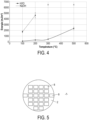
- the results are represented by the dotted line curve at figure 4 showing the bonding energy on the y-axis and the annealing temperature in degrees Celsius on the x-axis.
- the bonding energy is measured for example with the double-lever method with imposed displacement in an anhydrous atmosphere as described in the article by F. Fournel, L. Continni, C. Morales, J. Da Fonseca, H. Moriceau, F. Rieutord, A. Barthelemy, and I. Radu, Journal of Applied Physics 111, 104907 (2012 ).
- the temperature is applied to assembly 7 for 2 hours and then the measurement is carried out on assembly 7 after returning to room temperature.
- Control examples were carried out in parallel on direct bonds identical to those of the invention but in the absence of strong base molecules on the bonding surfaces (solid curve).
- temperatures of 100°C, 200°C, 300°C and 500°C were evaluated for the direct bonding assisted by basic molecules and the bonding energy is significantly higher than that of the unassisted direct bonding from 100°C.
- the gap widens particularly after a bonding anneal at 200°C, for which the assisted direct bonding according to the invention reaches 4.5 J/m 2 while the unassisted bonding has a bonding energy of less than 0.5 J/m 2 .
- the measurement of the bonding energy could not be performed after the annealings at 300 °C and 500 °C because the application of the measurement method requiring the separation of the substrates led to the breakage of the silicon substrates (illustrated by crosses on the graph of the figure 4 ).
- the direct bonding energy is higher than the silicon fracture energy of 5 J/m 2 . It therefore exceeds this value from 300°C.
- Unassisted direct bonding only reaches 2.2 J/m 2 after a bonding anneal at 500°C.
- the first substrate 1 provided in step a) is vignetted into several first vignettes 8 whose exposed faces are first hydrophilic bonding surfaces 3.
- the first vignettes 8 are bonded according to the method previously described on the second full-wafer substrate 2 according to a chip-to-wafer bonding also known in English terminology by the expression 'chip to wafer'.
- the second substrate 2 is also vignetted into several second vignettes and the method of the invention allows the direct bonding of the first vignettes 8 and the second vignettes.
- first hydrophilic bonding surface 3 and the second hydrophilic bonding surface 4 are formed at least in part by a hydrophilic film 5 of copper oxide.
- first and second silicon substrates 1,2 with a diameter of 300 mm and a thickness of 775 micrometers are prepared so as to have hybrid copper-oxide surfaces that can be bonded by direct bonding.
- These first and second hydrophilic bonding surfaces 3,4 are typically composed of copper pads with a side of 2.5 micrometers separated by 2.5 micrometers of SiO2. This is then referred to as a hybrid surface with a “pitch” of 5 micrometers.
- a solution of NaOH at 10-5 g/cm3 is deposited in deionized water by spin coating according to step b).
- the two hydrophilic surfaces 3,4 are then dried by centrifugation at 2000 rpm for 45s according to step c). Then the two surfaces 3,4 are brought into contact.
- the bonding wave is then approximately 12 s to cross the 300 mm which is equivalent to bonding without this basic molecule.
- the assembly 7 is annealed at 400°C for 2 hours. No particular defect is observed by acoustic microscopy.
- the solution implemented by the present invention makes it possible to significantly increase the direct bonding energy, even with large diameter substrates, with or without heat treatment carried out at low temperature, so that it is applicable to substrates comprising temperature-sensitive components.
- the method is simple to implement and the steps of depositing the basic solution and drying the surfaces are rapid.
- the basic solutions used are inexpensive, the basic quantities are very small, which does not modify the adhesion energy of the substrates 1,2 and allows spontaneous direct bonding.
Landscapes
- Engineering & Computer Science (AREA)
- Computer Hardware Design (AREA)
- Power Engineering (AREA)
- Microelectronics & Electronic Packaging (AREA)
- General Physics & Mathematics (AREA)
- Manufacturing & Machinery (AREA)
- Physics & Mathematics (AREA)
- Condensed Matter Physics & Semiconductors (AREA)
- Chemical & Material Sciences (AREA)
- Ceramic Engineering (AREA)
- Pressure Welding/Diffusion-Bonding (AREA)
- Laminated Bodies (AREA)
- Adhesives Or Adhesive Processes (AREA)
- Lining Or Joining Of Plastics Or The Like (AREA)
- Ceramic Products (AREA)
Claims (10)
- Verfahren zur direkten Verklebung zwischen zwei Substraten (1, 2), wobei das Verfahren die Schritte umfasst zum:a) Bereitstellen eines ersten Substrats (1) und eines zweiten Substrats (2), die eine erste hydrophile Klebefläche (3) und/oder eine zweite hydrophile Klebefläche (4) umfassen,b) Abscheiden auf der ersten und/oder auf der zweiten hydrophilen Klebefläche (3, 4) einer basischen Lösung (B) bestehend aus Molekülen der Starken Basen und deionisiertem Wasser,c) Trocknen der ersten und/oder der zweiten hydrophilen Klebefläche (3, 4), so dass eine Konzentration zwischen etwa 109 Atome/cm2 und 1015 Atome/cm2 von Kation erreicht wird, die aus den Molekülen der Starken Basen der ersten und/oder der zweiten hydrophilen Klebefläche (3, 4) hervorgegangen sind,d) In-Kontakt-bringen der ersten und der zweiten hydrophilen Klebefläche (3, 4), so dass eine spontane direkte Verklebung erhalten wird und eine Verbindung (7) des ersten Substrats (1) mit dem zweiten Substrat (2), eine Grenzfläche der direkten Verklebung (6) umfassend.
- Verfahren zur direkten Verklebung nach Anspruch 1, wobei der Schritt c) der Trocknung derart durchgeführt wird, dass die erste hydrophile Klebefläche (3) und die zweite hydrophile Klebefläche (4) mit einer bis fünf H2O-Monoatomschichten bedeckt sind.
- Verfahren zur direkten Verklebung nach Anspruch 1 oder 2, wobei die Moleküle der Starken Basen aus den Basen LiOH, NaOH, KOH, RbOH, CsOH, Mg(OH)2, Ca(OH)2, Sr(OH)2, Ba(OH)2 und einer Mischung dieser Basen ausgewählt sind.
- Verfahren zur direkten Verklebung nach einem der Ansprüche 1 bis 3, wobei die basische Lösung (B) eine Konzentration der Moleküle der Starken Basen zwischen 10-8 mol/l und 10-2 mol/l in deionisiertem Wasser aufweist.
- Verfahren zur direkten Verklebung nach einem der Ansprüche 1 bis 4, wobei der Schritt c) durch Zentrifugieren durchgeführt wird, beispielsweise mit einer Rotationsgeschwindigkeit von etwa 2000 Umdrehungen/min, der ersten und/oder der zweiten hydrophilen Klebefläche (3, 4), und insbesondere für 45 Sek.
- Verfahren zur direkten Verklebung nach einem der Ansprüche 1 bis 5, einen Schritt e) der Anwendung einer Wärmebehandlung an die Verbindung (7) umfassend, die in Schritt d) erhalten wurde, bei einer Temperatur zwischen 50 °C und 500 °C, besonders zwischen 50 und 350 °C und insbesondere zwischen 60 und 250 °C.
- Verfahren zur direkten Verklebung nach einem der Ansprüche 1 bis 6, wobei das erste und das zweite Substrat (1, 2) aus Silizium bestehen.
- Verfahren zur direkten Verklebung nach einem der Ansprüche 1 bis 7, wobei die erste hydrophile Klebefläche (3) und/oder die zweite hydrophile Klebefläche (4) mindestens teilweise durch einen hydrophilen Film (5) aus einem Material gebildet sind, das aus Siliziumoxid, Siliziumnitrid, Kupferoxid und einer Mischung dieser Materialien ausgewählt ist.
- Verfahren zur direkten Verklebung nach einem der Ansprüche 1 bis 8, wobei das erste Substrat (1), das Schritt a) bereitstellt, eine oder mehrere erste Vignetten (8) umfasst, die aus der Vignettierung des ersten Substrats (1) stammen, so dass eine direkte Verklebung einer oder mehrerer erster Vignetten mit dem zweiten Substrat (2) erhalten wird.
- Verbindung (7), ein erstes Substrat (1) und ein zweites Substrat (2) aus Silizium umfassend, die eine erste hydrophile Klebefläche (3) beziehungsweise eine zweite hydrophile Klebefläche (4) umfassen, wobei die erste und die zweite hydrophile Klebefläche (3, 4) durch direkte Verklebung verklebt sind, wobei die Moleküle der Starken Basen mit einer Konzentration zwischen etwa 109 Atome/cm2 und 1015 Atome/cm2 angeordnet sind, und besonders zwischen etwa 1010 Atome/cm2 und 1014 Atome/cm2, an der Grenzfläche der direkten Verklebung (6) zwischen der ersten und der zweiten hydrophilen Klebefläche (3, 4).
Applications Claiming Priority (1)
| Application Number | Priority Date | Filing Date | Title |
|---|---|---|---|
| FR2205048A FR3136107B1 (fr) | 2022-05-25 | 2022-05-25 | Procédé de collage direct assisté par une base forte |
Publications (3)
| Publication Number | Publication Date |
|---|---|
| EP4283659A1 EP4283659A1 (de) | 2023-11-29 |
| EP4283659B1 true EP4283659B1 (de) | 2025-01-29 |
| EP4283659C0 EP4283659C0 (de) | 2025-01-29 |
Family
ID=82319650
Family Applications (1)
| Application Number | Title | Priority Date | Filing Date |
|---|---|---|---|
| EP23173764.4A Active EP4283659B1 (de) | 2022-05-25 | 2023-05-16 | Verfahren zum direkt-bonden, mit hilfe starker basen |
Country Status (5)
| Country | Link |
|---|---|
| US (1) | US20230386894A1 (de) |
| EP (1) | EP4283659B1 (de) |
| JP (1) | JP2023174562A (de) |
| CN (1) | CN117133667A (de) |
| FR (1) | FR3136107B1 (de) |
Families Citing this family (2)
| Publication number | Priority date | Publication date | Assignee | Title |
|---|---|---|---|---|
| WO2025140983A1 (fr) * | 2023-12-29 | 2025-07-03 | Soitec | Procédé de collage direct entre deux substrats |
| FR3159042A1 (fr) * | 2024-02-07 | 2025-08-08 | Soitec | Procédé de collage direct entre deux substrats |
Family Cites Families (4)
| Publication number | Priority date | Publication date | Assignee | Title |
|---|---|---|---|---|
| FR1312269A (fr) | 1962-01-18 | 1962-12-14 | Philips Nv | Générateur de bruit pour ondes très courtes, équipé d'un tube à décharge dans le gaz |
| FR2868599B1 (fr) * | 2004-03-30 | 2006-07-07 | Soitec Silicon On Insulator | Traitement chimique optimise de type sc1 pour le nettoyage de plaquettes en materiau semiconducteur |
| US7919391B2 (en) * | 2004-12-24 | 2011-04-05 | S.O.I.Tec Silicon On Insulator Technologies | Methods for preparing a bonding surface of a semiconductor wafer |
| FR3102771B1 (fr) * | 2019-10-31 | 2021-10-08 | Commissariat Energie Atomique | Procédé de collage de deux surfaces hydrophiles |
-
2022
- 2022-05-25 FR FR2205048A patent/FR3136107B1/fr active Active
-
2023
- 2023-05-11 US US18/196,184 patent/US20230386894A1/en active Pending
- 2023-05-16 EP EP23173764.4A patent/EP4283659B1/de active Active
- 2023-05-16 JP JP2023080561A patent/JP2023174562A/ja active Pending
- 2023-05-24 CN CN202310592658.5A patent/CN117133667A/zh active Pending
Also Published As
| Publication number | Publication date |
|---|---|
| JP2023174562A (ja) | 2023-12-07 |
| FR3136107B1 (fr) | 2024-05-31 |
| CN117133667A (zh) | 2023-11-28 |
| US20230386894A1 (en) | 2023-11-30 |
| EP4283659A1 (de) | 2023-11-29 |
| FR3136107A1 (fr) | 2023-12-01 |
| EP4283659C0 (de) | 2025-01-29 |
Similar Documents
| Publication | Publication Date | Title |
|---|---|---|
| EP2304787B1 (de) | Stickstoffplasma-oberflächenbehandlung in einem direktbindungsverfahren | |
| EP4283659B1 (de) | Verfahren zum direkt-bonden, mit hilfe starker basen | |
| EP1879220A2 (de) | Direktes hydrophobes Verfahren zum Kleben von zwei Substraten zur Verwendung in der Elektronik, Optik und Opto-Elektronik. | |
| EP2764535B1 (de) | Verfahren zum doppelten Übertragen einer Schicht | |
| WO2021084188A1 (fr) | Procédé de collage de deux surfaces hydrophiles | |
| WO2009087290A1 (fr) | Procédé de fabrication d'une structure micro-électronique impliquant un collage moléculaire | |
| FR2923079A1 (fr) | Substrats soi avec couche fine isolante enterree | |
| FR2823599A1 (fr) | Substrat demomtable a tenue mecanique controlee et procede de realisation | |
| FR2938975A1 (fr) | Procede de realisation d'une heterostructure de type silicium sur saphir | |
| EP4283658B1 (de) | Verfahren zum direkten bonden mit hilfe eines basischen moleküls | |
| EP4283660B1 (de) | Direktes klebeverfahren mit unterstützung durch kationische elemente | |
| EP3425657B1 (de) | Verfahren zur herstellung einer schnittstelle für die temporäre montage eines mikroelektronischen supports und eines bedienungsgriffs, und entsprechende temporäre montageschnittstelle | |
| FR2888402A1 (fr) | Procede d'assemblage de substrats par depot d'une couche mince de collage d'oxyde ou de nitrure et structure ainsi assemblee | |
| FR3029352A1 (fr) | Procede d'assemblage de deux substrats | |
| EP3166132A1 (de) | Herstellungsverfahren von substraten | |
| EP3939078A1 (de) | Verfahren zur übertragung einer nutzschicht auf ein trägersubstrat | |
| EP4088309B1 (de) | Verfahren zum verbinden zweier halbleitersubstrate | |
| FR2880186A1 (fr) | Procede de traitement d'une surface de plaquette | |
| EP3961684B1 (de) | Verfahren zur herstellung eines substrats zum temporären verkleben eines substrats | |
| EP3503173A1 (de) | Übertragungsverfahren einer nutzschicht | |
| EP3721467A1 (de) | Verfahren zur herstellung des restes eines donorsubstrats, nach diesem verfahren hergestelltes substrat und verwendung eines solchen substrats | |
| FR3059149A1 (fr) | Procede de fabrication d'un film mince a base d'inp ou de gaas |
Legal Events
| Date | Code | Title | Description |
|---|---|---|---|
| PUAI | Public reference made under article 153(3) epc to a published international application that has entered the european phase |
Free format text: ORIGINAL CODE: 0009012 |
|
| STAA | Information on the status of an ep patent application or granted ep patent |
Free format text: STATUS: REQUEST FOR EXAMINATION WAS MADE |
|
| 17P | Request for examination filed |
Effective date: 20230516 |
|
| AK | Designated contracting states |
Kind code of ref document: A1 Designated state(s): AL AT BE BG CH CY CZ DE DK EE ES FI FR GB GR HR HU IE IS IT LI LT LU LV MC ME MK MT NL NO PL PT RO RS SE SI SK SM TR |
|
| GRAP | Despatch of communication of intention to grant a patent |
Free format text: ORIGINAL CODE: EPIDOSNIGR1 |
|
| STAA | Information on the status of an ep patent application or granted ep patent |
Free format text: STATUS: GRANT OF PATENT IS INTENDED |
|
| RIC1 | Information provided on ipc code assigned before grant |
Ipc: H01L 21/762 20060101ALI20240807BHEP Ipc: H01L 21/18 20060101AFI20240807BHEP |
|
| RIN1 | Information on inventor provided before grant (corrected) |
Inventor name: MORALES, CHRISTOPHE Inventor name: LARREY, VINCENT Inventor name: CALVEZ, AZILIZ Inventor name: FOURNEL, FRANK |
|
| INTG | Intention to grant announced |
Effective date: 20240829 |
|
| RAP3 | Party data changed (applicant data changed or rights of an application transferred) |
Owner name: COMMISSARIAT A L'ENERGIE ATOMIQUE ET AUX ENERGIESALTERNATIVES |
|
| RAP3 | Party data changed (applicant data changed or rights of an application transferred) |
Owner name: COMMISSARIAT A L'ENERGIE ATOMIQUE ET AUX ENERGIESALTERNATIVES |
|
| GRAS | Grant fee paid |
Free format text: ORIGINAL CODE: EPIDOSNIGR3 |
|
| GRAA | (expected) grant |
Free format text: ORIGINAL CODE: 0009210 |
|
| STAA | Information on the status of an ep patent application or granted ep patent |
Free format text: STATUS: THE PATENT HAS BEEN GRANTED |
|
| AK | Designated contracting states |
Kind code of ref document: B1 Designated state(s): AL AT BE BG CH CY CZ DE DK EE ES FI FR GB GR HR HU IE IS IT LI LT LU LV MC ME MK MT NL NO PL PT RO RS SE SI SK SM TR |
|
| REG | Reference to a national code |
Ref country code: GB Ref legal event code: FG4D Free format text: NOT ENGLISH |
|
| REG | Reference to a national code |
Ref country code: CH Ref legal event code: EP |
|
| REG | Reference to a national code |
Ref country code: DE Ref legal event code: R096 Ref document number: 602023001848 Country of ref document: DE |
|
| REG | Reference to a national code |
Ref country code: IE Ref legal event code: FG4D Free format text: LANGUAGE OF EP DOCUMENT: FRENCH |
|
| U01 | Request for unitary effect filed |
Effective date: 20250221 |
|
| U07 | Unitary effect registered |
Designated state(s): AT BE BG DE DK EE FI FR IT LT LU LV MT NL PT RO SE SI Effective date: 20250227 |
|
| U20 | Renewal fee for the european patent with unitary effect paid |
Year of fee payment: 3 Effective date: 20250520 |
|
| PG25 | Lapsed in a contracting state [announced via postgrant information from national office to epo] |
Ref country code: RS Free format text: LAPSE BECAUSE OF FAILURE TO SUBMIT A TRANSLATION OF THE DESCRIPTION OR TO PAY THE FEE WITHIN THE PRESCRIBED TIME-LIMIT Effective date: 20250429 |
|
| PG25 | Lapsed in a contracting state [announced via postgrant information from national office to epo] |
Ref country code: PL Free format text: LAPSE BECAUSE OF FAILURE TO SUBMIT A TRANSLATION OF THE DESCRIPTION OR TO PAY THE FEE WITHIN THE PRESCRIBED TIME-LIMIT Effective date: 20250129 |
|
| PG25 | Lapsed in a contracting state [announced via postgrant information from national office to epo] |
Ref country code: ES Free format text: LAPSE BECAUSE OF FAILURE TO SUBMIT A TRANSLATION OF THE DESCRIPTION OR TO PAY THE FEE WITHIN THE PRESCRIBED TIME-LIMIT Effective date: 20250129 |
|
| PG25 | Lapsed in a contracting state [announced via postgrant information from national office to epo] |
Ref country code: IS Free format text: LAPSE BECAUSE OF FAILURE TO SUBMIT A TRANSLATION OF THE DESCRIPTION OR TO PAY THE FEE WITHIN THE PRESCRIBED TIME-LIMIT Effective date: 20250529 Ref country code: NO Free format text: LAPSE BECAUSE OF FAILURE TO SUBMIT A TRANSLATION OF THE DESCRIPTION OR TO PAY THE FEE WITHIN THE PRESCRIBED TIME-LIMIT Effective date: 20250429 |
|
| PG25 | Lapsed in a contracting state [announced via postgrant information from national office to epo] |
Ref country code: HR Free format text: LAPSE BECAUSE OF FAILURE TO SUBMIT A TRANSLATION OF THE DESCRIPTION OR TO PAY THE FEE WITHIN THE PRESCRIBED TIME-LIMIT Effective date: 20250129 |
|
| PG25 | Lapsed in a contracting state [announced via postgrant information from national office to epo] |
Ref country code: GR Free format text: LAPSE BECAUSE OF FAILURE TO SUBMIT A TRANSLATION OF THE DESCRIPTION OR TO PAY THE FEE WITHIN THE PRESCRIBED TIME-LIMIT Effective date: 20250430 |
|
| PG25 | Lapsed in a contracting state [announced via postgrant information from national office to epo] |
Ref country code: SM Free format text: LAPSE BECAUSE OF FAILURE TO SUBMIT A TRANSLATION OF THE DESCRIPTION OR TO PAY THE FEE WITHIN THE PRESCRIBED TIME-LIMIT Effective date: 20250129 |
|
| PG25 | Lapsed in a contracting state [announced via postgrant information from national office to epo] |
Ref country code: CZ Free format text: LAPSE BECAUSE OF FAILURE TO SUBMIT A TRANSLATION OF THE DESCRIPTION OR TO PAY THE FEE WITHIN THE PRESCRIBED TIME-LIMIT Effective date: 20250129 |
|
| PG25 | Lapsed in a contracting state [announced via postgrant information from national office to epo] |
Ref country code: SK Free format text: LAPSE BECAUSE OF FAILURE TO SUBMIT A TRANSLATION OF THE DESCRIPTION OR TO PAY THE FEE WITHIN THE PRESCRIBED TIME-LIMIT Effective date: 20250129 |