EP4280280A1 - Array substrate and method for manufacturing same, display panel, and display device - Google Patents
Array substrate and method for manufacturing same, display panel, and display device Download PDFInfo
- Publication number
- EP4280280A1 EP4280280A1 EP22921720.3A EP22921720A EP4280280A1 EP 4280280 A1 EP4280280 A1 EP 4280280A1 EP 22921720 A EP22921720 A EP 22921720A EP 4280280 A1 EP4280280 A1 EP 4280280A1
- Authority
- EP
- European Patent Office
- Prior art keywords
- common
- base substrate
- contact pad
- electrode
- via hole
- Prior art date
- Legal status (The legal status is an assumption and is not a legal conclusion. Google has not performed a legal analysis and makes no representation as to the accuracy of the status listed.)
- Granted
Links
Images


Classifications
-
- G—PHYSICS
- G02—OPTICS
- G02F—OPTICAL DEVICES OR ARRANGEMENTS FOR THE CONTROL OF LIGHT BY MODIFICATION OF THE OPTICAL PROPERTIES OF THE MEDIA OF THE ELEMENTS INVOLVED THEREIN; NON-LINEAR OPTICS; FREQUENCY-CHANGING OF LIGHT; OPTICAL LOGIC ELEMENTS; OPTICAL ANALOGUE/DIGITAL CONVERTERS
- G02F1/00—Devices or arrangements for the control of the intensity, colour, phase, polarisation or direction of light arriving from an independent light source, e.g. switching, gating or modulating; Non-linear optics
- G02F1/01—Devices or arrangements for the control of the intensity, colour, phase, polarisation or direction of light arriving from an independent light source, e.g. switching, gating or modulating; Non-linear optics for the control of the intensity, phase, polarisation or colour
- G02F1/13—Devices or arrangements for the control of the intensity, colour, phase, polarisation or direction of light arriving from an independent light source, e.g. switching, gating or modulating; Non-linear optics for the control of the intensity, phase, polarisation or colour based on liquid crystals, e.g. single liquid crystal display cells
- G02F1/133—Constructional arrangements; Operation of liquid crystal cells; Circuit arrangements
- G02F1/136—Liquid crystal cells structurally associated with a semi-conducting layer or substrate, e.g. cells forming part of an integrated circuit
- G02F1/1362—Active matrix addressed cells
- G02F1/136286—Wiring, e.g. gate line, drain line
-
- G—PHYSICS
- G02—OPTICS
- G02F—OPTICAL DEVICES OR ARRANGEMENTS FOR THE CONTROL OF LIGHT BY MODIFICATION OF THE OPTICAL PROPERTIES OF THE MEDIA OF THE ELEMENTS INVOLVED THEREIN; NON-LINEAR OPTICS; FREQUENCY-CHANGING OF LIGHT; OPTICAL LOGIC ELEMENTS; OPTICAL ANALOGUE/DIGITAL CONVERTERS
- G02F1/00—Devices or arrangements for the control of the intensity, colour, phase, polarisation or direction of light arriving from an independent light source, e.g. switching, gating or modulating; Non-linear optics
- G02F1/01—Devices or arrangements for the control of the intensity, colour, phase, polarisation or direction of light arriving from an independent light source, e.g. switching, gating or modulating; Non-linear optics for the control of the intensity, phase, polarisation or colour
- G02F1/13—Devices or arrangements for the control of the intensity, colour, phase, polarisation or direction of light arriving from an independent light source, e.g. switching, gating or modulating; Non-linear optics for the control of the intensity, phase, polarisation or colour based on liquid crystals, e.g. single liquid crystal display cells
- G02F1/133—Constructional arrangements; Operation of liquid crystal cells; Circuit arrangements
- G02F1/136—Liquid crystal cells structurally associated with a semi-conducting layer or substrate, e.g. cells forming part of an integrated circuit
- G02F1/1362—Active matrix addressed cells
-
- G—PHYSICS
- G02—OPTICS
- G02F—OPTICAL DEVICES OR ARRANGEMENTS FOR THE CONTROL OF LIGHT BY MODIFICATION OF THE OPTICAL PROPERTIES OF THE MEDIA OF THE ELEMENTS INVOLVED THEREIN; NON-LINEAR OPTICS; FREQUENCY-CHANGING OF LIGHT; OPTICAL LOGIC ELEMENTS; OPTICAL ANALOGUE/DIGITAL CONVERTERS
- G02F1/00—Devices or arrangements for the control of the intensity, colour, phase, polarisation or direction of light arriving from an independent light source, e.g. switching, gating or modulating; Non-linear optics
- G02F1/01—Devices or arrangements for the control of the intensity, colour, phase, polarisation or direction of light arriving from an independent light source, e.g. switching, gating or modulating; Non-linear optics for the control of the intensity, phase, polarisation or colour
- G02F1/13—Devices or arrangements for the control of the intensity, colour, phase, polarisation or direction of light arriving from an independent light source, e.g. switching, gating or modulating; Non-linear optics for the control of the intensity, phase, polarisation or colour based on liquid crystals, e.g. single liquid crystal display cells
- G02F1/133—Constructional arrangements; Operation of liquid crystal cells; Circuit arrangements
- G02F1/136—Liquid crystal cells structurally associated with a semi-conducting layer or substrate, e.g. cells forming part of an integrated circuit
- G02F1/1362—Active matrix addressed cells
- G02F1/136222—Colour filters incorporated in the active matrix substrate
-
- G—PHYSICS
- G02—OPTICS
- G02F—OPTICAL DEVICES OR ARRANGEMENTS FOR THE CONTROL OF LIGHT BY MODIFICATION OF THE OPTICAL PROPERTIES OF THE MEDIA OF THE ELEMENTS INVOLVED THEREIN; NON-LINEAR OPTICS; FREQUENCY-CHANGING OF LIGHT; OPTICAL LOGIC ELEMENTS; OPTICAL ANALOGUE/DIGITAL CONVERTERS
- G02F1/00—Devices or arrangements for the control of the intensity, colour, phase, polarisation or direction of light arriving from an independent light source, e.g. switching, gating or modulating; Non-linear optics
- G02F1/01—Devices or arrangements for the control of the intensity, colour, phase, polarisation or direction of light arriving from an independent light source, e.g. switching, gating or modulating; Non-linear optics for the control of the intensity, phase, polarisation or colour
- G02F1/13—Devices or arrangements for the control of the intensity, colour, phase, polarisation or direction of light arriving from an independent light source, e.g. switching, gating or modulating; Non-linear optics for the control of the intensity, phase, polarisation or colour based on liquid crystals, e.g. single liquid crystal display cells
- G02F1/133—Constructional arrangements; Operation of liquid crystal cells; Circuit arrangements
- G02F1/136—Liquid crystal cells structurally associated with a semi-conducting layer or substrate, e.g. cells forming part of an integrated circuit
- G02F1/1362—Active matrix addressed cells
- G02F1/136286—Wiring, e.g. gate line, drain line
- G02F1/13629—Multilayer wirings
-
- G—PHYSICS
- G02—OPTICS
- G02F—OPTICAL DEVICES OR ARRANGEMENTS FOR THE CONTROL OF LIGHT BY MODIFICATION OF THE OPTICAL PROPERTIES OF THE MEDIA OF THE ELEMENTS INVOLVED THEREIN; NON-LINEAR OPTICS; FREQUENCY-CHANGING OF LIGHT; OPTICAL LOGIC ELEMENTS; OPTICAL ANALOGUE/DIGITAL CONVERTERS
- G02F1/00—Devices or arrangements for the control of the intensity, colour, phase, polarisation or direction of light arriving from an independent light source, e.g. switching, gating or modulating; Non-linear optics
- G02F1/01—Devices or arrangements for the control of the intensity, colour, phase, polarisation or direction of light arriving from an independent light source, e.g. switching, gating or modulating; Non-linear optics for the control of the intensity, phase, polarisation or colour
- G02F1/13—Devices or arrangements for the control of the intensity, colour, phase, polarisation or direction of light arriving from an independent light source, e.g. switching, gating or modulating; Non-linear optics for the control of the intensity, phase, polarisation or colour based on liquid crystals, e.g. single liquid crystal display cells
- G02F1/133—Constructional arrangements; Operation of liquid crystal cells; Circuit arrangements
- G02F1/136—Liquid crystal cells structurally associated with a semi-conducting layer or substrate, e.g. cells forming part of an integrated circuit
- G02F1/1362—Active matrix addressed cells
- G02F1/136286—Wiring, e.g. gate line, drain line
- G02F1/136295—Materials; Compositions; Manufacture processes
-
- H—ELECTRICITY
- H10—SEMICONDUCTOR DEVICES; ELECTRIC SOLID-STATE DEVICES NOT OTHERWISE PROVIDED FOR
- H10D—INORGANIC ELECTRIC SEMICONDUCTOR DEVICES
- H10D86/00—Integrated devices formed in or on insulating or conducting substrates, e.g. formed in silicon-on-insulator [SOI] substrates or on stainless steel or glass substrates
- H10D86/01—Manufacture or treatment
- H10D86/021—Manufacture or treatment of multiple TFTs
- H10D86/0212—Manufacture or treatment of multiple TFTs comprising manufacture, treatment or coating of substrates
-
- H—ELECTRICITY
- H10—SEMICONDUCTOR DEVICES; ELECTRIC SOLID-STATE DEVICES NOT OTHERWISE PROVIDED FOR
- H10D—INORGANIC ELECTRIC SEMICONDUCTOR DEVICES
- H10D86/00—Integrated devices formed in or on insulating or conducting substrates, e.g. formed in silicon-on-insulator [SOI] substrates or on stainless steel or glass substrates
- H10D86/40—Integrated devices formed in or on insulating or conducting substrates, e.g. formed in silicon-on-insulator [SOI] substrates or on stainless steel or glass substrates characterised by multiple TFTs
- H10D86/441—Interconnections, e.g. scanning lines
-
- H—ELECTRICITY
- H10—SEMICONDUCTOR DEVICES; ELECTRIC SOLID-STATE DEVICES NOT OTHERWISE PROVIDED FOR
- H10D—INORGANIC ELECTRIC SEMICONDUCTOR DEVICES
- H10D86/00—Integrated devices formed in or on insulating or conducting substrates, e.g. formed in silicon-on-insulator [SOI] substrates or on stainless steel or glass substrates
- H10D86/40—Integrated devices formed in or on insulating or conducting substrates, e.g. formed in silicon-on-insulator [SOI] substrates or on stainless steel or glass substrates characterised by multiple TFTs
- H10D86/60—Integrated devices formed in or on insulating or conducting substrates, e.g. formed in silicon-on-insulator [SOI] substrates or on stainless steel or glass substrates characterised by multiple TFTs wherein the TFTs are in active matrices
-
- G—PHYSICS
- G02—OPTICS
- G02F—OPTICAL DEVICES OR ARRANGEMENTS FOR THE CONTROL OF LIGHT BY MODIFICATION OF THE OPTICAL PROPERTIES OF THE MEDIA OF THE ELEMENTS INVOLVED THEREIN; NON-LINEAR OPTICS; FREQUENCY-CHANGING OF LIGHT; OPTICAL LOGIC ELEMENTS; OPTICAL ANALOGUE/DIGITAL CONVERTERS
- G02F1/00—Devices or arrangements for the control of the intensity, colour, phase, polarisation or direction of light arriving from an independent light source, e.g. switching, gating or modulating; Non-linear optics
- G02F1/01—Devices or arrangements for the control of the intensity, colour, phase, polarisation or direction of light arriving from an independent light source, e.g. switching, gating or modulating; Non-linear optics for the control of the intensity, phase, polarisation or colour
- G02F1/13—Devices or arrangements for the control of the intensity, colour, phase, polarisation or direction of light arriving from an independent light source, e.g. switching, gating or modulating; Non-linear optics for the control of the intensity, phase, polarisation or colour based on liquid crystals, e.g. single liquid crystal display cells
- G02F1/133—Constructional arrangements; Operation of liquid crystal cells; Circuit arrangements
- G02F1/1333—Constructional arrangements; Manufacturing methods
- G02F1/1343—Electrodes
- G02F1/134309—Electrodes characterised by their geometrical arrangement
- G02F1/134363—Electrodes characterised by their geometrical arrangement for applying an electric field parallel to the substrate, i.e. in-plane switching [IPS]
-
- G—PHYSICS
- G02—OPTICS
- G02F—OPTICAL DEVICES OR ARRANGEMENTS FOR THE CONTROL OF LIGHT BY MODIFICATION OF THE OPTICAL PROPERTIES OF THE MEDIA OF THE ELEMENTS INVOLVED THEREIN; NON-LINEAR OPTICS; FREQUENCY-CHANGING OF LIGHT; OPTICAL LOGIC ELEMENTS; OPTICAL ANALOGUE/DIGITAL CONVERTERS
- G02F1/00—Devices or arrangements for the control of the intensity, colour, phase, polarisation or direction of light arriving from an independent light source, e.g. switching, gating or modulating; Non-linear optics
- G02F1/01—Devices or arrangements for the control of the intensity, colour, phase, polarisation or direction of light arriving from an independent light source, e.g. switching, gating or modulating; Non-linear optics for the control of the intensity, phase, polarisation or colour
- G02F1/13—Devices or arrangements for the control of the intensity, colour, phase, polarisation or direction of light arriving from an independent light source, e.g. switching, gating or modulating; Non-linear optics for the control of the intensity, phase, polarisation or colour based on liquid crystals, e.g. single liquid crystal display cells
- G02F1/133—Constructional arrangements; Operation of liquid crystal cells; Circuit arrangements
- G02F1/1333—Constructional arrangements; Manufacturing methods
- G02F1/1343—Electrodes
- G02F1/134309—Electrodes characterised by their geometrical arrangement
- G02F1/134372—Electrodes characterised by their geometrical arrangement for fringe field switching [FFS] where the common electrode is not patterned
-
- G—PHYSICS
- G02—OPTICS
- G02F—OPTICAL DEVICES OR ARRANGEMENTS FOR THE CONTROL OF LIGHT BY MODIFICATION OF THE OPTICAL PROPERTIES OF THE MEDIA OF THE ELEMENTS INVOLVED THEREIN; NON-LINEAR OPTICS; FREQUENCY-CHANGING OF LIGHT; OPTICAL LOGIC ELEMENTS; OPTICAL ANALOGUE/DIGITAL CONVERTERS
- G02F2201/00—Constructional arrangements not provided for in groups G02F1/00 - G02F7/00
- G02F2201/40—Arrangements for improving the aperture ratio
Definitions
- This application relates to the field of display panel, and particularly to an array substrate and a method for manufacturing the same, a display panel, and a display device.
- TFT-LCD Thin Film Transistor Liquid Crystal Displays
- the TFT-LCD includes a Data Line (DL)/source line, a Scan Line (SL)/gate line, a common-electrode line, and a Thin Film Transistor (TFT).
- DL Data Line
- SL Scan Line
- TFT Thin Film Transistor
- the SL is perpendicular to DL
- the common-electrode line is parallel to and spaced apart from the SL. Since signals transmitted on various signal lines are different, these signal lines need to be isolated from one another, and these signal lines are opaque since they are made of metal, as a result, an aperture ratio of a pixel is relatively low, which leads to a low display brightness of the display panel.
- the disclosure provides an array substrate.
- the array substrate includes a base substrate, a stacked structure, a common-electrode line, and a conductive structure.
- the base substrate has a first surface and a second surface opposite to the first surface.
- the stacked structure is disposed on the first surface of the base substrate.
- the stacked structure includes a contact pad, a common-electrode layer, and a gate line.
- the contact pad is disposed on the first surface of the base substrate.
- the base substrate defines a first via hole at a position corresponding to the contact pad, where the first via hole penetrates the first surface and the second surface of the base substrate.
- the common-electrode layer is connected with the contact pad.
- the gate line is isolated from the common-electrode layer and the contact pad.
- the common-electrode line is disposed on the second surface of the base substrate, where an orthographic projection of the gate line on a plane where the common-electrode line is located at least partially overlaps with the common-electrode line.
- the conductive structure is connected with the contact pad, and connected to the common-electrode line through the first via hole.
- the gate line is disposed on the first surface of the array substrate and the common-electrode line is disposed on the second surface of the array substrate opposite to the first surface, and the gate line at least partially overlaps with the common-electrode line, which can reduce a wiring area on the first surface of the array substrate, thereby increasing an area of a pixel-electrode layer in each pixel unit and increasing an aperture ratio of the pixel unit.
- the disclosure further provides a display panel.
- the display panel includes a color-film substrate and an array substrate.
- the array substrate is opposite to the color-film substrate.
- the array substrate includes a base substrate, a stacked structure, a common-electrode line, and a conductive structure.
- the base substrate has a first surface and a second surface opposite to the first surface.
- the stacked structure is disposed on the first surface of the base substrate.
- the stacked structure includes a contact pad, a common-electrode layer, and a gate line.
- the contact pad is disposed on the first surface of the base substrate.
- the base substrate defines a first via hole at a position corresponding to the contact pad, where the first via hole penetrates the first surface and the second surface of the base substrate.
- the common-electrode layer is connected with the contact pad.
- the gate line is isolated from the common-electrode layer and the contact pad.
- the common-electrode line is disposed on the second surface of the base substrate, where an orthographic projection of the gate line on a plane where the common-electrode line is located at least partially overlaps with the common-electrode line.
- the conductive structure is connected with the contact pad, and connected to the common-electrode line through the first via hole.
- orientations or positional relationships indicated by the terms “upper”, “lower”, “left”, “right”, and the like are based on orientations or positional relationships illustrated in the accompanying drawings, and are only for convenience of describing the disclosure and simplifying the description, rather than indicating or implying that the referred device or element must have a specific orientation, be constructed and operated in a specific orientation, and therefore should not be construed as a limitation of the disclosure.
- the terms “first”, “second”, and the like are used for descriptive only and should not be construed to indicate or imply relative importance.
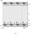
- FIG. 1 is a schematic top view of an existing array substrate 100".
- the array substrate 100" includes multiple gate lines 121" (i.e., scan lines) extending along a first direction (an OX direction illustrated in figures), multiple common-electrode lines 201" extending along the first direction, and multiple source lines 131" (i.e., data lines) extending along a second direction (an OY direction illustrated in figures).
- the multiple gate lines 121" intersect the multiple source lines 131", to define multiple pixel units 300" arranged in an array.
- Each pixel unit 300" includes a Thin Film Transistor (TFT) 50", a pixel-electrode layer 30", and a common-electrode layer (not illustrated).
- TFT Thin Film Transistor
- a source 52" of the TFT 50" is connected with a source line 131" near the source 52
- a drain 53" of the TFT 50” is connected with the pixel-electrode layer 30
- a gate 51" of the TFT 50" is connected with a gate line 121" near the gate 51".
- the common-electrode layer is connected with a common-electrode line 201" nearby.
- the gate lines 121", the source lines 131", and the common-electrode lines 201" of the existing array substrate 100" each occupy part of a wiring area and each are made of metal and opaque, an area of the pixel-electrode layer 30" in each pixel unit 300" is relatively small, which leads to a low aperture ratio of the pixel unit 300" of the array substrate in 100".
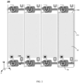
- the disclosure provides an array substrate 100, referring to FIG. 2 to FIG. 4 .
- a common-electrode line 201 and a gate line 121 are respectively disposed on two opposite surfaces of the array substrate 100, and a projection of the gate line 121 on a plane where the common-electrode line is located at least partially overlaps with the common-electrode line, which can reduce a wiring area in the array substrate 100, thereby increasing an area of a pixel-electrode layer 30 in each pixel unit 300 and increasing an aperture ratio of the pixel unit 300.
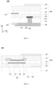
- the array substrate 100 includes a base substrate 10, a stacked structure 200, a common-electrode line 201, and a conductive structure 40.
- the base substrate 10 has a first surface 110 and a second surface 120 opposite to the first surface 110.
- the stacked structure 200 is disposed on the first surface 110 of the base substrate 10.
- the stacked structure 200 includes a contact pad 101, a common-electrode layer 20, and a gate line 121.
- the contact pad 101 is disposed on the first surface 110 of the base substrate 10 and connected with the common-electrode layer 20.
- the gate line 121 is isolated from the common-electrode layer 20 and the contact pad 101.
- the base substrate 10 defines a first via hole 102 at a position corresponding to the contact pad 101, and the first via hole 102 penetrates the first surface 110 and the second surface 120 of the base substrate 10.
- the conductive structure 40 is connected with the contact pad 101 and connected with the common-electrode line 201 through the first via hole 102.
- the first via hole 102 may be a circular hole or a square hole, or be in other shapes, which is not limited herein.
- the common-electrode line 201 is disposed on the second surface 120 of the base substrate 10.
- the orthographic projection of the gate line 121 on the plane where the common-electrode line 201 is located completely covers the common-electrode line 201.
- the gate line 121 includes multiple gate lines 121 extending along the first direction
- the common-electrode line 201 includes multiple common-electrode lines 201 extending along the first direction
- the multiple gate lines 121 are in one-to-one correspondence with the multiple common-electrode lines 201.
- a larger wiring area on the first surface of the array substrate 100 can be reduced, which facilitates increasing the aperture ratio of the pixel unit 300.
- a projection of the gate line 121 on the plane where a corresponding common-electrode line 201 is located completely overlaps with the common-electrode line 201.
- the wiring area on the first surface 110 can be reduced by 10% and the area of the pixel-electrode layer 30 in each pixel unit 300 can be increased by 10%, therefore, the aperture ratio of the pixel unit 300 can be increased by about 10%.
- each pixel unit 300 includes a contact pad 101 and a common-electrode layer 20, the base substrate 10 defines a first via hole 102 at a position corresponding to each contact pad 101, and contact pads 101 are connected with common-electrode layers 20 in one-to-one correspondence.
- the base substrate 10 may be a hard substrate made of a light-guiding and non-metallic material with certain firmness, such as glass, quartz, common resin, etc., or the base substrate 10 may also be a flexible substrate made of a flexible material such as Polyimide (PI).
- the common-electrode layer 20 may be made of a metal oxide such as Indium Tin Oxide (ITO), Indium Zinc Oxide (IZO), etc.
- the conductive structure 40 may be formed through a silver paste printing process.
- the common-electrode line 201, the gate line 121, and the contact pad 101 may be made of same or different materials, exemplarily, a conductive metal, for example, at least one of molybdenum, aluminum, chromium, tungsten, tantalum, titanium, or copper.
- a conductive metal for example, at least one of molybdenum, aluminum, chromium, tungsten, tantalum, titanium, or copper.
- the gate line 121 is disposed on the first surface 110 of the array substrate 100 and the common-electrode line 201 is disposed on the second surface 120 of the array substrate 100 opposite to the first surface 110, and the gate line 121 at least partially overlaps with the common-electrode line 201, which can reduce the wiring area on the first surface 110 of the array substrate 100, thereby increasing the area of the pixel-electrode layer 30 in each pixel unit 300 and increasing the aperture ratio of the pixel unit 300.
- the number of layered structures in the stacked structure 200 and positional relationships between the layered structures can be designed according to requirements, which are not limited in the disclosure.
- the gate line 121 and the contact pad 101 of the stacked structure 200 are disposed in a same layer, and are disposed on the first surface 110 of the base substrate 10.
- the stacked structure 200 further includes a first insulating layer 11, a drain-source layer, an active layer 54, a second insulating layer 12, a third insulating layer 13, and a pixel-electrode layer 30.
- the gate line 121 and a gate 51 are disposed in a same layer.
- the first insulating layer 11 covers the gate line 121, the gate 51, and the contact pad 101.
- the source-drain layer and the active layer 54 are disposed on the first insulating layer 11.
- the drain-source layer includes a source 52 and a drain 53.
- a gate 51, a source 52, a drain 53, and an active layer 54 in a same pixel unit 300 together form a TFT 50.
- the second insulating layer 12 covers the source-drain layer and the active layer 54.
- the common-electrode layer 20 is disposed on the second insulating layer 12.
- the third insulating layer 13 covers the common-electrode layer 20.
- the pixel-electrode layer 30 is disposed on the third insulating layer 13. Exemplarily, an orthographic projection of the pixel-electrode layer 30 on the base substrate 10 overlaps with an orthographic projection of the common-electrode layer 20 on the base substrate 10.
- first insulating layer 11 and the second insulating layer 12 define a second via hole 122 at positions corresponding to the contact pad 101.
- the common-electrode layer 20 is connected with the contact pad 101 through the second via hole 122.
- a first insulating layer 11 and a second insulating layer 12 in each pixel unit 300 define a second via hole 122, and common-electrode layers 20 are connected with contact pads 101 in one-to-one correspondence through a corresponding second via hole 122.
- a common-electrode layer 20' and a contact pad 101' are disposed in a same layer and connected with each other, and are disposed on a first surface 110' of a base substrate 10'.
- the stacked structure 200' further includes a first insulating layer 11', a second insulating layer 12', a drain-source layer, an active layer 54', a third insulating layer 13', and a pixel-electrode layer 30'.
- the first insulating layer 11' covers the contact pad 101' and the common-electrode layer 20'.
- a gate line 121' and a gate 51' are disposed in a same layer, and are disposed on the first insulating layer 11'.
- the second insulating layer 12' covers the gate line 121' and the gate 51'.
- the drain-source layer is disposed on the second insulating layer 12'.
- the drain-source layer includes a source 52' and a drain 53'.
- a gate 51', a source 52', a drain 53', and an active layer 54' in a same pixel unit 300 jointly constitute a TFT 50'.
- the third insulating layer 13' covers the drain-source layer.
- the pixel-electrode layer 30' is disposed on the third insulating layer 13'.
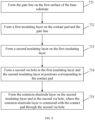
- implementations of the disclosure further provide a method for manufacturing an array substrate. As illustrated in FIG. 7 , the method includes the following.
- a base substrate 10 is provided.
- the base substrate 10 has a first surface 110 and a second surface 120 opposite to the first surface 110.
- the base substrate 10 may be a hard substrate made of a light-guiding and non-metallic material with certain firmness, such as glass, quartz, common resin, etc., or the base substrate 10 may also be a flexible substrate made of a flexible material such as PI.
- a stacked structure 200 is formed on the first surface 110 of the base substrate 10.
- the stacked structure 200 includes a contact pad 101, a common-electrode layer 20, and a gate line 121, where the contact pad 101 is formed on the first surface 110 of the base substrate 10, the common-electrode layer 20 is connected with the contact pad 101, and the gate line 121 is isolated from the common-electrode layer 20 and the contact pad 101.
- a first via hole 102 is formed in the base substrate 10 at a position corresponding to the contact pad 101, where the first via hole 102 penetrates the first surface 110 and second surface 120 of the base substrate 10, and the contact pad 101 is exposed to outside of the first via hole 102.
- the first via hole 102 may be a circular hole or a square hole, or be in other shapes, which is not limited herein. Since an area of a single pixel unit 300 is relatively small, the size of the first via hole 102 needs to be controlled within a certain range. Exemplarily, the first via hole 102 is a circular hole with a diameter of about 10um, or a square hole with a side length of about 10um. If the base substrate 10 is made of glass, HF and O 2 can be used to etch glass (SiO 2 ), and the first via hole 102 can be formed through a cyclic dry etching process, where the cyclic dry etching process belongs to an existing technology, which will not be repeated herein.
- each pixel unit 300 defines a first via hole 102
- the number of first via holes 102 on the base substrate 10 is relatively large and arrangement of the first via holes 102 is relatively dense.
- the base substrate 10 is made of glass, the requirement for the cyclic dry etching process is relatively high, otherwise, the base substrate may be broken.
- the base substrate 10 may also be made of polyimide, so that the first via hole 102 can be formed through exposure and development, as such, the process is relatively simple, and the base substrate will not be broken. Specifically, a mask with a pattern is covered on the second surface 120 of the base substrate 10.
- An ultraviolet light selectively irradiates the second surface 120 of the base substrate 10, and then developer is used to remove polyimide of part of the base substrate 10 that was illuminated or polyimide of part of the base substrate 10 that was not illuminated, to make the pattern on the mask be formed on the base substrate 10, that is, the first via hole 102 is formed.
- a common-electrode line 201 is formed on the second surface 120 of the base substrate 10, where an orthographic projection of the gate line 121 on a plane where the common-electrode line 201 is located at least partially overlaps with the common-electrode line 201.
- the common-electrode line 201 can be formed through a patterning process.
- multiple common-electrode lines 201 in one-to-one correspondence with multiple gate lines 121 are formed on the second surface 120 of the base substrate 10 through a patterning process, where orthographic projections of the multiple gate lines 121 on a plane where the common-electrode lines 201 are located completely cover the multiple common-electrode lines 201, or, orthographic projections of the multiple common-electrode lines 201 on a plane where the gate lines 121 are located completely cover the multiple gate lines 121.
- the "patterning process" of implementations of the disclosure includes film deposition, photoresist coating, mask exposure, developing, etching, photoresist stripping, and other processes.
- the deposition may adopt any one or more of sputtering, evaporation, chemical vapor deposition.
- the coating may be any one or more of spray coating and spin coating.
- the etching may be any one or more of dry etching and wet etching.
- a conductive structure 40 is formed in the first via hole 102 and at a preset position of the second surface 120 of the base substrate 10, where the contact pad 101 is connected to a common-electrode line 201 near the first via hole 102 through the conductive structure 40.
- the conductive structure 40 is formed through a silver paste printing process, where the contact pad 101 in each pixel unit 300 is connected to a nearby common-electrode line 201 through a corresponding first via hole 102.
- the disclosure does not limit an order for executing the operations at 73 to 75, as long as the operations at 75 are after the operations at 73.
- the operations at 74 are performed first, then the operations at 73, and finally the operations at 75.
- the operations at 73 are performed first, then the operations at 75, and finally the operations at 74.
- the number of layered structures in the stacked structure 200 and positional relationships between the layered structures can be designed according to requirements.
- the operations at 72 correspond to features of the stacked structure 200, which is not limited herein. Exemplarily, in an implementation, as illustrated in FIG. 8 , the operations at 72 specifically include the following.
- the contact pad 101 and the gate line 121 are formed on the first surface 110 of the base substrate 10.
- a gate 51 is also formed on the first surface 110 of the base substrate 10.
- the contact pad 101, the gate line 121, and the gate 51 are made of a same material, and can be formed through a patterning process.
- a contact pad 101 is formed in each pixel unit 300.
- a first insulating layer 11 is formed on the contact pad 101 and the gate line 121.
- the first insulating layer 11 also covers the gate 51.
- the first insulating layer 11 is made of a material such as silicon nitride, silicon oxide, or silicon oxynitride.
- a second insulating layer 12 is formed on the first insulating layer 11.
- the operations at 723 specifically include the following.
- a drain-source layer and an active layer 54 are formed on the first insulating layer 11.
- the active layer 54 may be a semiconductor active layer or an oxide active layer.
- the active layer 54 is a semiconductor active layer made of a semiconductor material such as amorphous silicon or polycrystalline silicon.
- the active layer 54 is formed through a patterning process, and the drain-source layer is formed through another patterning process.
- the second insulating layer 12 is formed on the drain-source layer and the active layer 54.
- the second insulating layer 12 is made of a material such as silicon nitride, silicon oxide, or silicon oxynitride.
- a second via hole 122 is formed in the first insulating layer and the second insulating layer 12 at positions corresponding to the contact pad 101, where the contact pad 101 is exposed to outside of the second via hole 122.
- the first insulating layer and the second insulating layer 12 in each pixel unit 300 define a second via hole 122.
- the common-electrode layer 20 is formed on the second insulating layer 12 and in the second via hole, where the common-electrode layer 20 is connected with the contact pad 101 through the second via hole. Specifically, the common-electrode layer 20 in each pixel unit 300 is connected with a corresponding contact pad 101 through the second via hole 122.
- the gate line 121 is formed on the first surface 110 of the array substrate 100 and the common-electrode line 201 is formed on the second surface 120 of the array substrate 100 opposite to the first surface 110, and the gate line 121 at least partially overlaps with the common-electrode line 201, which can reduce a wiring area on the first surface 110 of the array substrate 100, thereby increasing an area of the pixel-electrode layer 30 in each pixel unit 300 and increasing an aperture ratio of the pixel unit 300.
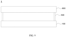
- the disclosure further provides a display panel 1.
- the display panel 1 includes a color-film substrate 600, the above array substrate 100, and a sealant 500.
- the array substrate 100 is disposed opposite to the color-film substrate 600.
- the display panel 1 further includes a liquid crystal layer (not illustrated) filled between the color-film substrate 600 and the array substrate 100.
- the sealant 500 is disposed around the liquid crystal layer, and configured to seal the liquid crystal layer between the array substrate 100 and the color-film substrate 600.
- the display panel 1 may further include other structures, for example, a lower polarizer (not illustrated), an upper polarizer (not illustrated), etc., which is not limited herein.
- the display panel 1 may be a TFT-LCD with various liquid crystal driving and display modes, including but not limited to, a Twisted Nematic (TN) panel, a Vertical Alignment (VA) panel, an In-Plane Switching (IPS) panel, etc.
- TN Twisted Nematic
- VA Vertical Alignment
- IPS In-Plane Switching
- the disclosure further provides a display device (not illustrated).
- the display device includes the above display panel 1.
Landscapes
- Physics & Mathematics (AREA)
- Nonlinear Science (AREA)
- Engineering & Computer Science (AREA)
- Microelectronics & Electronic Packaging (AREA)
- Mathematical Physics (AREA)
- Chemical & Material Sciences (AREA)
- Crystallography & Structural Chemistry (AREA)
- General Physics & Mathematics (AREA)
- Optics & Photonics (AREA)
- Manufacturing & Machinery (AREA)
- Liquid Crystal (AREA)
- Devices For Indicating Variable Information By Combining Individual Elements (AREA)
Abstract
Description
- This application claims priority to
Chinese Application Patent Serial No. 202210072612.6, entitled "ARRAY SUBSTRATE AND METHOD FOR MANUFACTURING THE SAME, DISPLAY PANEL, AND DISPLAY DEVICE", and filed January 21, 2022 - This application relates to the field of display panel, and particularly to an array substrate and a method for manufacturing the same, a display panel, and a display device.
- The statements herein merely provide background information related to the disclosure and may not necessarily constitute the related art. With development and progress of technologies, Thin Film Transistor Liquid Crystal Displays (TFT-LCD) have become the most widely used display in the market, especially in LCD TVs.
- At present, the TFT-LCD includes a Data Line (DL)/source line, a Scan Line (SL)/gate line, a common-electrode line, and a Thin Film Transistor (TFT). In an existing TFT LCD, the SL is perpendicular to DL, and the common-electrode line is parallel to and spaced apart from the SL. Since signals transmitted on various signal lines are different, these signal lines need to be isolated from one another, and these signal lines are opaque since they are made of metal, as a result, an aperture ratio of a pixel is relatively low, which leads to a low display brightness of the display panel.
- The disclosure provides an array substrate. The array substrate includes a base substrate, a stacked structure, a common-electrode line, and a conductive structure. The base substrate has a first surface and a second surface opposite to the first surface. The stacked structure is disposed on the first surface of the base substrate. The stacked structure includes a contact pad, a common-electrode layer, and a gate line. The contact pad is disposed on the first surface of the base substrate. The base substrate defines a first via hole at a position corresponding to the contact pad, where the first via hole penetrates the first surface and the second surface of the base substrate. The common-electrode layer is connected with the contact pad. The gate line is isolated from the common-electrode layer and the contact pad. The common-electrode line is disposed on the second surface of the base substrate, where an orthographic projection of the gate line on a plane where the common-electrode line is located at least partially overlaps with the common-electrode line. The conductive structure is connected with the contact pad, and connected to the common-electrode line through the first via hole.
- According to the array substrate of the disclosure, the gate line is disposed on the first surface of the array substrate and the common-electrode line is disposed on the second surface of the array substrate opposite to the first surface, and the gate line at least partially overlaps with the common-electrode line, which can reduce a wiring area on the first surface of the array substrate, thereby increasing an area of a pixel-electrode layer in each pixel unit and increasing an aperture ratio of the pixel unit.
- The disclosure further provides a display panel. The display panel includes a color-film substrate and an array substrate. The array substrate is opposite to the color-film substrate. The array substrate includes a base substrate, a stacked structure, a common-electrode line, and a conductive structure. The base substrate has a first surface and a second surface opposite to the first surface. The stacked structure is disposed on the first surface of the base substrate. The stacked structure includes a contact pad, a common-electrode layer, and a gate line. The contact pad is disposed on the first surface of the base substrate. The base substrate defines a first via hole at a position corresponding to the contact pad, where the first via hole penetrates the first surface and the second surface of the base substrate. The common-electrode layer is connected with the contact pad. The gate line is isolated from the common-electrode layer and the contact pad. The common-electrode line is disposed on the second surface of the base substrate, where an orthographic projection of the gate line on a plane where the common-electrode line is located at least partially overlaps with the common-electrode line. The conductive structure is connected with the contact pad, and connected to the common-electrode line through the first via hole.
- Additional aspects and advantages of the disclosure will be illustrated in part from the following description, and the other part of the additional aspects and the advantages of the disclosure will become apparent from the following description, or may be learned by practice of the disclosure.
-
-
FIG. 1 is a schematic top view of an existing array substrate. -
FIG. 2 is a schematic top view of an array substrate provided in implementations of the disclosure. -
FIG. 3 is a schematic cross-sectional structure diagram of the structure illustrated inFIG. 2 along line A-A. -
FIG. 4 is another schematic cross-sectional structure diagram of the array substrate illustrated inFIG. 2 . -
FIG. 5 is another schematic cross-sectional structure diagram of the structure illustrated inFIG. 2 along line A-A. -
FIG. 6 is another schematic cross-sectional structure diagram of the array substrate illustrated inFIG. 2 . -
FIG. 7 is a schematic flowchart illustrating a method for manufacturing an array substrate provided in implementations of the disclosure. -
FIG. 8 is a detailed flowchart of operations at 72 illustrated inFIG. 7 . -
FIG. 9 is a schematic structural diagram illustrating a display panel provided in implementations of the disclosure. - The disclosure will be further depicted below with reference to specific implementations and accompanying drawings.
- Hereinafter, technical solutions of implementations of the disclosure will be depicted in a clear and comprehensive manner with reference to accompanying drawings intended for these implementations. Apparently, implementations described below merely illustrate some implementations, rather than all implementations, of the disclosure. All other implementations obtained by those of ordinary skill in the art based on the implementations of the disclosure without creative efforts shall fall within the protection scope of the disclosure.
- In description of the disclosure, it should be noted that, orientations or positional relationships indicated by the terms "upper", "lower", "left", "right", and the like are based on orientations or positional relationships illustrated in the accompanying drawings, and are only for convenience of describing the disclosure and simplifying the description, rather than indicating or implying that the referred device or element must have a specific orientation, be constructed and operated in a specific orientation, and therefore should not be construed as a limitation of the disclosure. In addition, the terms "first", "second", and the like are used for descriptive only and should not be construed to indicate or imply relative importance.
- Referring to
FIG. 1, FIG. 1 is a schematic top view of anexisting array substrate 100". Thearray substrate 100" includesmultiple gate lines 121" (i.e., scan lines) extending along a first direction (an OX direction illustrated in figures), multiple common-electrode lines 201" extending along the first direction, andmultiple source lines 131" (i.e., data lines) extending along a second direction (an OY direction illustrated in figures). Themultiple gate lines 121" intersect themultiple source lines 131", to definemultiple pixel units 300" arranged in an array. Eachpixel unit 300" includes a Thin Film Transistor (TFT) 50", a pixel-electrode layer 30", and a common-electrode layer (not illustrated). Asource 52" of the TFT 50" is connected with asource line 131" near thesource 52", adrain 53" of the TFT 50" is connected with the pixel-electrode layer 30", and agate 51" of the TFT 50" is connected with agate line 121" near thegate 51". The common-electrode layer is connected with a common-electrode line 201" nearby. Since thegate lines 121", thesource lines 131", and the common-electrode lines 201" of the existingarray substrate 100" each occupy part of a wiring area and each are made of metal and opaque, an area of the pixel-electrode layer 30" in eachpixel unit 300" is relatively small, which leads to a low aperture ratio of thepixel unit 300" of the array substrate in 100". - In order to solve the problem of the low aperture ratio of the pixel unit in the existing array substrate, the disclosure provides an
array substrate 100, referring toFIG. 2 to FIG. 4 . According to thearray substrate 100 of the disclosure, a common-electrode line 201 and agate line 121 are respectively disposed on two opposite surfaces of thearray substrate 100, and a projection of thegate line 121 on a plane where the common-electrode line is located at least partially overlaps with the common-electrode line, which can reduce a wiring area in thearray substrate 100, thereby increasing an area of a pixel-electrode layer 30 in eachpixel unit 300 and increasing an aperture ratio of thepixel unit 300. - Specifically, referring to
FIG. 3 , thearray substrate 100 includes abase substrate 10, astacked structure 200, a common-electrode line 201, and aconductive structure 40. Thebase substrate 10 has afirst surface 110 and asecond surface 120 opposite to thefirst surface 110. - The
stacked structure 200 is disposed on thefirst surface 110 of thebase substrate 10. Thestacked structure 200 includes acontact pad 101, a common-electrode layer 20, and agate line 121. Thecontact pad 101 is disposed on thefirst surface 110 of thebase substrate 10 and connected with the common-electrode layer 20. Thegate line 121 is isolated from the common-electrode layer 20 and thecontact pad 101. Thebase substrate 10 defines a first viahole 102 at a position corresponding to thecontact pad 101, and the first viahole 102 penetrates thefirst surface 110 and thesecond surface 120 of thebase substrate 10. Theconductive structure 40 is connected with thecontact pad 101 and connected with the common-electrode line 201 through the first viahole 102. The first viahole 102 may be a circular hole or a square hole, or be in other shapes, which is not limited herein. - The common-
electrode line 201 is disposed on thesecond surface 120 of thebase substrate 10. An orthographic projection of thegate line 121 on a plane where the common-electrode line 201 is located at least partially overlaps with the common-electrode line 201. In implementations of the disclosure, the orthographic projection of thegate line 121 on the plane where the common-electrode line 201 is located completely covers the common-electrode line 201. Specifically, thegate line 121 includesmultiple gate lines 121 extending along the first direction, the common-electrode line 201 includes multiple common-electrode lines 201 extending along the first direction, and themultiple gate lines 121 are in one-to-one correspondence with the multiple common-electrode lines 201. It can be understood that, when an overlapping area of thegate lines 121 and the common-electrode lines 201 is larger, a larger wiring area on the first surface of thearray substrate 100 can be reduced, which facilitates increasing the aperture ratio of thepixel unit 300. Exemplarily, for each of thegate lines 121, a projection of thegate line 121 on the plane where a corresponding common-electrode line 201 is located completely overlaps with the common-electrode line 201. Since a wiring area of the common-electrode lines 201 in the existing array substrate occupies about 10% of a pixel area, by adopting thearray substrate 100 of the disclosure, the wiring area on thefirst surface 110 can be reduced by 10% and the area of the pixel-electrode layer 30 in eachpixel unit 300 can be increased by 10%, therefore, the aperture ratio of thepixel unit 300 can be increased by about 10%. - It should be noted that, in implementations of the disclosure, each
pixel unit 300 includes acontact pad 101 and a common-electrode layer 20, thebase substrate 10 defines a first viahole 102 at a position corresponding to eachcontact pad 101, andcontact pads 101 are connected with common-electrode layers 20 in one-to-one correspondence. - Exemplarily, the
base substrate 10 may be a hard substrate made of a light-guiding and non-metallic material with certain firmness, such as glass, quartz, common resin, etc., or thebase substrate 10 may also be a flexible substrate made of a flexible material such as Polyimide (PI). The common-electrode layer 20 may be made of a metal oxide such as Indium Tin Oxide (ITO), Indium Zinc Oxide (IZO), etc. Theconductive structure 40 may be formed through a silver paste printing process. The common-electrode line 201, thegate line 121, and thecontact pad 101 may be made of same or different materials, exemplarily, a conductive metal, for example, at least one of molybdenum, aluminum, chromium, tungsten, tantalum, titanium, or copper. - According to the
array substrate 100 of the disclosure, thegate line 121 is disposed on thefirst surface 110 of thearray substrate 100 and the common-electrode line 201 is disposed on thesecond surface 120 of thearray substrate 100 opposite to thefirst surface 110, and thegate line 121 at least partially overlaps with the common-electrode line 201, which can reduce the wiring area on thefirst surface 110 of thearray substrate 100, thereby increasing the area of the pixel-electrode layer 30 in eachpixel unit 300 and increasing the aperture ratio of thepixel unit 300. - It should be noted that, the number of layered structures in the
stacked structure 200 and positional relationships between the layered structures can be designed according to requirements, which are not limited in the disclosure. - Exemplarily, in an implementation, as illustrated in
FIG. 3 and FIG. 4 , thegate line 121 and thecontact pad 101 of the stackedstructure 200 are disposed in a same layer, and are disposed on thefirst surface 110 of thebase substrate 10. Thestacked structure 200 further includes a first insulatinglayer 11, a drain-source layer, anactive layer 54, a second insulatinglayer 12, a third insulatinglayer 13, and a pixel-electrode layer 30. - Specifically, the
gate line 121 and agate 51 are disposed in a same layer. The first insulatinglayer 11 covers thegate line 121, thegate 51, and thecontact pad 101. The source-drain layer and theactive layer 54 are disposed on the first insulatinglayer 11. The drain-source layer includes asource 52 and adrain 53. Agate 51, asource 52, adrain 53, and anactive layer 54 in asame pixel unit 300 together form aTFT 50. The second insulatinglayer 12 covers the source-drain layer and theactive layer 54. The common-electrode layer 20 is disposed on the second insulatinglayer 12. The third insulatinglayer 13 covers the common-electrode layer 20. The pixel-electrode layer 30 is disposed on the third insulatinglayer 13. Exemplarily, an orthographic projection of the pixel-electrode layer 30 on thebase substrate 10 overlaps with an orthographic projection of the common-electrode layer 20 on thebase substrate 10. - Further, the first insulating
layer 11 and the second insulatinglayer 12 define a second viahole 122 at positions corresponding to thecontact pad 101. The common-electrode layer 20 is connected with thecontact pad 101 through the second viahole 122. Specifically, in implementations of the disclosure, a first insulatinglayer 11 and a second insulatinglayer 12 in eachpixel unit 300 define a second viahole 122, and common-electrode layers 20 are connected withcontact pads 101 in one-to-one correspondence through a corresponding second viahole 122. - In another implementation, as illustrated in
FIG. 5 and FIG. 6 , a common-electrode layer 20' and a contact pad 101' are disposed in a same layer and connected with each other, and are disposed on a first surface 110' of a base substrate 10'. The stacked structure 200' further includes a first insulating layer 11', a second insulating layer 12', a drain-source layer, an active layer 54', a third insulating layer 13', and a pixel-electrode layer 30'. - Specifically, the first insulating layer 11' covers the contact pad 101' and the common-
electrode layer 20'. A gate line 121' and a gate 51' are disposed in a same layer, and are disposed on the first insulating layer 11'. The second insulating layer 12' covers the gate line 121' and the gate 51'. The drain-source layer is disposed on the second insulating layer 12'. The drain-source layer includes a source 52' and a drain 53'. A gate 51', a source 52', a drain 53', and an active layer 54' in asame pixel unit 300 jointly constitute a TFT 50'. The third insulating layer 13' covers the drain-source layer. The pixel-electrode layer 30' is disposed on the third insulating layer 13'. - Based on the same inventive concept, implementations of the disclosure further provide a method for manufacturing an array substrate. As illustrated in
FIG. 7 , the method includes the following. - At 71, a
base substrate 10 is provided. Thebase substrate 10 has afirst surface 110 and asecond surface 120 opposite to thefirst surface 110. Exemplarily, thebase substrate 10 may be a hard substrate made of a light-guiding and non-metallic material with certain firmness, such as glass, quartz, common resin, etc., or thebase substrate 10 may also be a flexible substrate made of a flexible material such as PI. - At 72, a
stacked structure 200 is formed on thefirst surface 110 of thebase substrate 10. Thestacked structure 200 includes acontact pad 101, a common-electrode layer 20, and agate line 121, where thecontact pad 101 is formed on thefirst surface 110 of thebase substrate 10, the common-electrode layer 20 is connected with thecontact pad 101, and thegate line 121 is isolated from the common-electrode layer 20 and thecontact pad 101. - At 73, a first via
hole 102 is formed in thebase substrate 10 at a position corresponding to thecontact pad 101, where the first viahole 102 penetrates thefirst surface 110 andsecond surface 120 of thebase substrate 10, and thecontact pad 101 is exposed to outside of the first viahole 102. - It should be noted that, the first via
hole 102 may be a circular hole or a square hole, or be in other shapes, which is not limited herein. Since an area of asingle pixel unit 300 is relatively small, the size of the first viahole 102 needs to be controlled within a certain range. Exemplarily, the first viahole 102 is a circular hole with a diameter of about 10um, or a square hole with a side length of about 10um. If thebase substrate 10 is made of glass, HF and O2 can be used to etch glass (SiO2), and the first viahole 102 can be formed through a cyclic dry etching process, where the cyclic dry etching process belongs to an existing technology, which will not be repeated herein. Since eachpixel unit 300 defines a first viahole 102, the number of first viaholes 102 on thebase substrate 10 is relatively large and arrangement of the first viaholes 102 is relatively dense. If thebase substrate 10 is made of glass, the requirement for the cyclic dry etching process is relatively high, otherwise, the base substrate may be broken. In the disclosure, thebase substrate 10 may also be made of polyimide, so that the first viahole 102 can be formed through exposure and development, as such, the process is relatively simple, and the base substrate will not be broken. Specifically, a mask with a pattern is covered on thesecond surface 120 of thebase substrate 10. An ultraviolet light selectively irradiates thesecond surface 120 of thebase substrate 10, and then developer is used to remove polyimide of part of thebase substrate 10 that was illuminated or polyimide of part of thebase substrate 10 that was not illuminated, to make the pattern on the mask be formed on thebase substrate 10, that is, the first viahole 102 is formed. - At 74, a common-
electrode line 201 is formed on thesecond surface 120 of thebase substrate 10, where an orthographic projection of thegate line 121 on a plane where the common-electrode line 201 is located at least partially overlaps with the common-electrode line 201. In implementations of the disclosure, exemplarily, the common-electrode line 201 can be formed through a patterning process. Specifically, multiple common-electrode lines 201 in one-to-one correspondence withmultiple gate lines 121 are formed on thesecond surface 120 of thebase substrate 10 through a patterning process, where orthographic projections of themultiple gate lines 121 on a plane where the common-electrode lines 201 are located completely cover the multiple common-electrode lines 201, or, orthographic projections of the multiple common-electrode lines 201 on a plane where thegate lines 121 are located completely cover the multiple gate lines 121. - The "patterning process" of implementations of the disclosure includes film deposition, photoresist coating, mask exposure, developing, etching, photoresist stripping, and other processes. The deposition may adopt any one or more of sputtering, evaporation, chemical vapor deposition. The coating may be any one or more of spray coating and spin coating. The etching may be any one or more of dry etching and wet etching. Each of the above processes belongs to an existing technology, which will not be repeated herein.
- At 75, a
conductive structure 40 is formed in the first viahole 102 and at a preset position of thesecond surface 120 of thebase substrate 10, where thecontact pad 101 is connected to a common-electrode line 201 near the first viahole 102 through theconductive structure 40. Exemplarily, theconductive structure 40 is formed through a silver paste printing process, where thecontact pad 101 in eachpixel unit 300 is connected to a nearby common-electrode line 201 through a corresponding first viahole 102. - It should be noted that, the disclosure does not limit an order for executing the operations at 73 to 75, as long as the operations at 75 are after the operations at 73. In another implementation, the operations at 74 are performed first, then the operations at 73, and finally the operations at 75. In yet another implementation, the operations at 73 are performed first, then the operations at 75, and finally the operations at 74.
- As mentioned above, the number of layered structures in the
stacked structure 200 and positional relationships between the layered structures can be designed according to requirements. The operations at 72 correspond to features of the stackedstructure 200, which is not limited herein. Exemplarily, in an implementation, as illustrated inFIG. 8 , the operations at 72 specifically include the following. - At 721, the
contact pad 101 and thegate line 121 are formed on thefirst surface 110 of thebase substrate 10. In this implementation, agate 51 is also formed on thefirst surface 110 of thebase substrate 10. Exemplarily, thecontact pad 101, thegate line 121, and thegate 51 are made of a same material, and can be formed through a patterning process. Specifically, acontact pad 101 is formed in eachpixel unit 300. - At 722, a first insulating
layer 11 is formed on thecontact pad 101 and thegate line 121. In this implementation, the first insulatinglayer 11 also covers thegate 51. Exemplarily, the first insulatinglayer 11 is made of a material such as silicon nitride, silicon oxide, or silicon oxynitride. - At 723, a second insulating
layer 12 is formed on the first insulatinglayer 11. - In implementations of the disclosure, the operations at 723 specifically include the following.
- At 723a, a drain-source layer and an
active layer 54 are formed on the first insulatinglayer 11. Theactive layer 54 may be a semiconductor active layer or an oxide active layer. For example, theactive layer 54 is a semiconductor active layer made of a semiconductor material such as amorphous silicon or polycrystalline silicon. Exemplarily, theactive layer 54 is formed through a patterning process, and the drain-source layer is formed through another patterning process. - At 723b, the second insulating
layer 12 is formed on the drain-source layer and theactive layer 54. Exemplarily, the second insulatinglayer 12 is made of a material such as silicon nitride, silicon oxide, or silicon oxynitride. - At 724, a second via
hole 122 is formed in the first insulating layer and the second insulatinglayer 12 at positions corresponding to thecontact pad 101, where thecontact pad 101 is exposed to outside of the second viahole 122. Specifically, the first insulating layer and the second insulatinglayer 12 in eachpixel unit 300 define a second viahole 122. - At 725, the common-
electrode layer 20 is formed on the second insulatinglayer 12 and in the second via hole, where the common-electrode layer 20 is connected with thecontact pad 101 through the second via hole. Specifically, the common-electrode layer 20 in eachpixel unit 300 is connected with acorresponding contact pad 101 through the second viahole 122. - According to the method for manufacturing the array substrate of the disclosure, the
gate line 121 is formed on thefirst surface 110 of thearray substrate 100 and the common-electrode line 201 is formed on thesecond surface 120 of thearray substrate 100 opposite to thefirst surface 110, and thegate line 121 at least partially overlaps with the common-electrode line 201, which can reduce a wiring area on thefirst surface 110 of thearray substrate 100, thereby increasing an area of the pixel-electrode layer 30 in eachpixel unit 300 and increasing an aperture ratio of thepixel unit 300. - Based on the same inventive concept, referring to
FIG. 9 , the disclosure further provides adisplay panel 1. Thedisplay panel 1 includes a color-film substrate 600, theabove array substrate 100, and asealant 500. Thearray substrate 100 is disposed opposite to the color-film substrate 600. Thedisplay panel 1 further includes a liquid crystal layer (not illustrated) filled between the color-film substrate 600 and thearray substrate 100. Thesealant 500 is disposed around the liquid crystal layer, and configured to seal the liquid crystal layer between thearray substrate 100 and the color-film substrate 600. Thedisplay panel 1 may further include other structures, for example, a lower polarizer (not illustrated), an upper polarizer (not illustrated), etc., which is not limited herein. - Exemplarily, the
display panel 1 may be a TFT-LCD with various liquid crystal driving and display modes, including but not limited to, a Twisted Nematic (TN) panel, a Vertical Alignment (VA) panel, an In-Plane Switching (IPS) panel, etc. - Based on the same inventive concept, the disclosure further provides a display device (not illustrated). The display device includes the
above display panel 1. - While the implementations of the disclosure have been illustrated and depicted above, it will be understood by those of ordinary skill in the art that various changes, modifications, substitutions, and alterations can be made to these implementations without departing from the principles and spirits of the disclosure. Therefore, the scope of the disclosure is defined by the appended claims and equivalents of the appended claims.
Claims (12)
- An array substrate, comprising:a base substrate having a first surface and a second surface opposite to the first surface; anda stacked structure disposed on the first surface of the base substrate, the stacked structure comprising:a contact pad disposed on the first surface of the base substrate, wherein the base substrate defines a first via hole at a position corresponding to the contact pad, the first via hole penetrating the first surface and the second surface of the base substrate;a common-electrode layer connected with the contact pad; anda gate line isolated from the common-electrode layer and the contact pad; and the array substrate further comprising:a common-electrode line disposed on the second surface of the base substrate, wherein an orthographic projection of the gate line on a plane where the common-electrode line is located at least partially overlaps with the common-electrode line; anda conductive structure connected with the contact pad, and connected to the common-electrode line through the first via hole.
- The array substrate of claim 1, whereinthe gate line and the contact pad of the stacked structure are disposed in a same layer, and are disposed on the first surface of the base substrate; andthe stacked structure further comprises:a first insulating layer covering the gate line and the contact pad; anda second insulating layer disposed on the first insulating layer, whereinthe common-electrode layer is disposed on the second insulating layer; the first insulating layer and the second insulating layer define a second via hole at positions corresponding to the contact pad, and the common-electrode layer is connected with the contact pad through the second via hole.
- The array substrate of claim 1, whereinthe common-electrode layer and the contact pad of the stacked structure are disposed in a same layer, and are disposed on the first surface of the base substrate; andthe stacked structure further comprises a first insulating layer, wherein the first insulating layer covers the common-electrode layer and the contact pad, and the gate line is disposed on the first insulating layer.
- The array substrate of claim 1, wherein the orthographic projection of the gate line on the plane where the common-electrode line is located completely covers the common-electrode line.
- The array substrate of claim 1, wherein an orthographic projection of the common-electrode line on a plane where the gate line is located completely covers the gate line.
- The array substrate of claim 1, wherein the base substrate is made of glass or polyimide.
- A method for manufacturing an array substrate, comprising:providing a base substrate, wherein the base substrate has a first surface and a second surface opposite to the first surface;forming a stacked structure on the first surface of the base substrate, wherein the stacked structure comprises a contact pad, a common-electrode layer, and a gate line, the contact pad is formed on the first surface of the base substrate, the common-electrode layer is connected with the contact pad, and the gate line is isolated from the common-electrode layer and the contact pad;forming a first via hole in the base substrate at a position corresponding to the contact pad, wherein the first via hole penetrates the first surface and the second surface of the base substrate;forming a common-electrode line on the second surface of the base substrate, wherein an orthographic projection of the gate line on a plane where the common-electrode line is located at least partially overlaps with the common-electrode line; andforming a conductive structure in the first via hole and at a preset position of the second surface of the base substrate, wherein the contact pad is connected to a common-electrode line near the first via hole through the conductive structure.
- The method of claim 7, wherein forming the stacked structure on the first surface of the base substrate comprises:forming the contact pad and the gate line on the first surface of the base substrate;forming a first insulating layer on the contact pad and the gate line;forming a second insulating layer on the first insulating layer;forming a second via hole in the first insulating layer and the second insulating layer at positions corresponding to the contact pad; andforming the common-electrode layer on the second insulating layer and in the second via hole, wherein the common-electrode layer is connected with the contact pad through the second via hole.
- The method of claim 8, wherein forming the common-electrode line on the second surface of the base substrate comprises:
forming on the second surface of the base substrate the common-electrode line corresponding to the gate line, wherein the orthographic projection of the gate line on the plane where the common-electrode line is located completely covers the common-electrode line. - The method of claim 8, wherein forming the common-electrode line on the second surface of the base substrate comprises:
forming on the second surface of the base substrate the common-electrode line corresponding to the gate line, wherein an orthographic projection of the common-electrode line on a plane where the gate line is located completely covers the gate line. - A display panel, comprising:a color-film substrate; andan array substrate opposite to the color-film substrate;the array substrate comprising:a base substrate having a first surface and a second surface opposite to the first surface; anda stacked structure disposed on the first surface of the base substrate, the stacked structure comprising:a contact pad disposed on the first surface of the base substrate, wherein the base substrate defines a first via hole at a position corresponding to the contact pad, the first via hole penetrating the first surface and the second surface of the base substrate;a common-electrode layer connected with the contact pad; anda gate line isolated from the common-electrode layer and the contact pad; andthe array substrate further comprising:a common-electrode line disposed on the second surface of the base substrate, wherein an orthographic projection of the gate line on a plane where the common-electrode line is located at least partially overlaps with the common-electrode line; anda conductive structure connected with the contact pad, and connected to the common-electrode line through the first via hole.
- A display device, comprising a display panel comprising:a color-film substrate; andan array substrate opposite to the color-film substrate;the array substrate comprising:a base substrate having a first surface and a second surface opposite to the first surface; anda stacked structure disposed on the first surface of the base substrate, the stacked structure comprising:a contact pad disposed on the first surface of the base substrate, wherein the base substrate defines a first via hole at a position corresponding to the contact pad, the first via hole penetrating the first surface and the second surface of the base substrate;a common-electrode layer connected with the contact pad; anda gate line isolated from the common-electrode layer and the contact pad; andthe array substrate further comprising:a common-electrode line disposed on the second surface of the base substrate, wherein an orthographic projection of the gate line on a plane where the common-electrode line is located at least partially overlaps with the common-electrode line; anda conductive structure connected with the contact pad, and connected to the common-electrode line through the first via hole.
Applications Claiming Priority (2)
| Application Number | Priority Date | Filing Date | Title |
|---|---|---|---|
| CN202210072612.6A CN114488636B (en) | 2022-01-21 | 2022-01-21 | Array substrate, manufacturing method thereof, display panel and display device |
| PCT/CN2022/141290 WO2023138299A1 (en) | 2022-01-21 | 2022-12-23 | Array substrate and method for manufacturing same, display panel, and display device |
Publications (3)
| Publication Number | Publication Date |
|---|---|
| EP4280280A1 true EP4280280A1 (en) | 2023-11-22 |
| EP4280280A4 EP4280280A4 (en) | 2024-07-17 |
| EP4280280B1 EP4280280B1 (en) | 2025-07-02 |
Family
ID=81472993
Family Applications (1)
| Application Number | Title | Priority Date | Filing Date |
|---|---|---|---|
| EP22921720.3A Active EP4280280B1 (en) | 2022-01-21 | 2022-12-23 | Array substrate and method for manufacturing same, display panel, and display device |
Country Status (4)
| Country | Link |
|---|---|
| US (1) | US11721705B1 (en) |
| EP (1) | EP4280280B1 (en) |
| CN (1) | CN114488636B (en) |
| WO (1) | WO2023138299A1 (en) |
Families Citing this family (2)
| Publication number | Priority date | Publication date | Assignee | Title |
|---|---|---|---|---|
| CN114488636B (en) * | 2022-01-21 | 2022-10-25 | 绵阳惠科光电科技有限公司 | Array substrate, manufacturing method thereof, display panel and display device |
| WO2025091285A1 (en) * | 2023-10-31 | 2025-05-08 | 京东方科技集团股份有限公司 | Array substrate and display panel |
Family Cites Families (17)
| Publication number | Priority date | Publication date | Assignee | Title |
|---|---|---|---|---|
| CN101517472B (en) * | 2006-09-19 | 2012-10-24 | 夏普株式会社 | Liquid crystal display apparatus |
| JP2014021449A (en) * | 2012-07-23 | 2014-02-03 | Panasonic Liquid Crystal Display Co Ltd | Liquid crystal display device and manufacturing method of liquid crystal display device |
| CN102967971B (en) * | 2012-11-02 | 2015-09-23 | 京东方科技集团股份有限公司 | Array base palte and display device |
| CN103278986B (en) * | 2013-04-01 | 2015-11-25 | 京东方科技集团股份有限公司 | The manufacture method of a kind of array base palte, display device and array base palte |
| CN103474436B (en) * | 2013-09-18 | 2016-03-09 | 京东方科技集团股份有限公司 | A kind of array base palte and preparation method thereof, display unit |
| CN103499906B (en) * | 2013-10-15 | 2017-02-15 | 京东方科技集团股份有限公司 | Array substrate, manufacturing method of array substrate and display device |
| CN105161495B (en) * | 2015-07-23 | 2018-09-11 | 京东方科技集团股份有限公司 | A kind of array substrate and preparation method thereof, display panel |
| CN104965336A (en) * | 2015-07-30 | 2015-10-07 | 深圳市华星光电技术有限公司 | COA array substrate and liquid crystal display panel |
| CN105226068B (en) * | 2015-09-14 | 2018-01-26 | 京东方科技集团股份有限公司 | A kind of double-sided display substrate and preparation method thereof and display device |
| US10241609B2 (en) * | 2015-12-30 | 2019-03-26 | Lg Display Co., Ltd. | Display device with touch sensor |
| TWI602306B (en) * | 2016-07-05 | 2017-10-11 | 群創光電股份有限公司 | Array substrate structure and display device |
| CN106409796A (en) * | 2016-10-25 | 2017-02-15 | 京东方科技集团股份有限公司 | Array substrate, manufacturing method thereof, display device and manufacturing method thereof |
| CN109786391B (en) * | 2017-11-10 | 2021-08-03 | 京东方科技集团股份有限公司 | Array substrate, manufacturing method thereof, and display device |
| CN110412806A (en) * | 2019-08-05 | 2019-11-05 | 京东方科技集团股份有限公司 | Array substrate and production method, display panel and production method and display device |
| CN111128025B (en) * | 2019-12-30 | 2021-11-26 | 厦门天马微电子有限公司 | Array substrate, display panel and display device |
| CN113433745A (en) * | 2021-06-07 | 2021-09-24 | 深圳市华星光电半导体显示技术有限公司 | Display panel and spliced display screen |
| CN114488636B (en) * | 2022-01-21 | 2022-10-25 | 绵阳惠科光电科技有限公司 | Array substrate, manufacturing method thereof, display panel and display device |
-
2022
- 2022-01-21 CN CN202210072612.6A patent/CN114488636B/en active Active
- 2022-12-23 EP EP22921720.3A patent/EP4280280B1/en active Active
- 2022-12-23 WO PCT/CN2022/141290 patent/WO2023138299A1/en not_active Ceased
- 2022-12-28 US US18/089,722 patent/US11721705B1/en active Active
Also Published As
| Publication number | Publication date |
|---|---|
| CN114488636B (en) | 2022-10-25 |
| EP4280280B1 (en) | 2025-07-02 |
| EP4280280A4 (en) | 2024-07-17 |
| US11721705B1 (en) | 2023-08-08 |
| US20230238391A1 (en) | 2023-07-27 |
| CN114488636A (en) | 2022-05-13 |
| WO2023138299A1 (en) | 2023-07-27 |
Similar Documents
| Publication | Publication Date | Title |
|---|---|---|
| US8379177B2 (en) | Array substrate for fringe field switching mode liquid crystal display device and method of fabricating the same | |
| US7733453B2 (en) | Method of fabricating a liquid crystal display device using a three mask process and double layer electrodes | |
| CN101299122B (en) | Liquid crystal display panel and manufacture method thereof | |
| US7894032B2 (en) | Liquid crystal display device having particular structure for data line, source electrode, drain electrode and pixel electrode | |
| US20120313845A1 (en) | Liquid crystal display device | |
| CN114787703B (en) | Array substrate and manufacturing method thereof | |
| US11721705B1 (en) | Array substrate and method for manufacturing the same, and display panel | |
| EP2790057A1 (en) | Thin film transistor array panel and manufacturing method thereof | |
| JP5007171B2 (en) | Thin film transistor array substrate, manufacturing method thereof, and display device | |
| US20090146151A1 (en) | Thin film transistor array substrate and method of manufacturing the same | |
| US12210252B2 (en) | Array substrate and manufacturing method therefor, and display panel | |
| US8817214B2 (en) | Liquid crystal display and fabricating method thereof | |
| KR20160133057A (en) | Liquid crystal display device and method for fabricating the same | |
| KR20130033827A (en) | Liquid crystal display device and method for manufacturing the same | |
| US7474372B2 (en) | Liquid crystal display having a protective alignment film and fabricating method thereof | |
| US20070001172A1 (en) | Liquid crystal display device and fabrication method thereof | |
| US9768206B2 (en) | Display substrate and method of manufacturing the same | |
| US20170343843A1 (en) | Liquid crystal display device and manufacturing method thereof | |
| US20200150472A1 (en) | Substrate for display device, display device, and method of producing substrate for display device | |
| US20200083386A1 (en) | Thin-film transistor substrate, liquid crystal display device, and organic electroluminescent display device | |
| KR101978789B1 (en) | Array substrate for display device and method of fabricating the same | |
| US8294862B2 (en) | Liquid crystal display device and method of fabricating the same | |
| CN107664893A (en) | Display base plate | |
| KR101186513B1 (en) | Liquid crystal display device and method of fabricating the same | |
| US10928691B2 (en) | Active matrix substrate comprising a first contact hole that overlaps with a counter electrode control line and passes through a flattening film and liquid crystal display with the same |
Legal Events
| Date | Code | Title | Description |
|---|---|---|---|
| STAA | Information on the status of an ep patent application or granted ep patent |
Free format text: STATUS: THE INTERNATIONAL PUBLICATION HAS BEEN MADE |
|
| PUAI | Public reference made under article 153(3) epc to a published international application that has entered the european phase |
Free format text: ORIGINAL CODE: 0009012 |
|
| STAA | Information on the status of an ep patent application or granted ep patent |
Free format text: STATUS: REQUEST FOR EXAMINATION WAS MADE |
|
| 17P | Request for examination filed |
Effective date: 20230817 |
|
| AK | Designated contracting states |
Kind code of ref document: A1 Designated state(s): AL AT BE BG CH CY CZ DE DK EE ES FI FR GB GR HR HU IE IS IT LI LT LU LV MC ME MK MT NL NO PL PT RO RS SE SI SK SM TR |
|
| REG | Reference to a national code |
Ref country code: DE Ref legal event code: R079 Free format text: PREVIOUS MAIN CLASS: H01L0027120000 Ipc: G02F0001136200 Ref document number: 602022017124 Country of ref document: DE |
|
| A4 | Supplementary search report drawn up and despatched |
Effective date: 20240618 |
|
| RIC1 | Information provided on ipc code assigned before grant |
Ipc: H01L 27/12 20060101ALI20240612BHEP Ipc: G02F 1/1343 20060101ALI20240612BHEP Ipc: G02F 1/1362 20060101AFI20240612BHEP |
|
| GRAP | Despatch of communication of intention to grant a patent |
Free format text: ORIGINAL CODE: EPIDOSNIGR1 |
|
| STAA | Information on the status of an ep patent application or granted ep patent |
Free format text: STATUS: GRANT OF PATENT IS INTENDED |
|
| RIC1 | Information provided on ipc code assigned before grant |
Ipc: H10D 86/60 20250101ALI20250108BHEP Ipc: H10D 86/40 20250101ALI20250108BHEP Ipc: G02F 1/1343 20060101ALI20250108BHEP Ipc: G02F 1/1362 20060101AFI20250108BHEP |
|
| DAV | Request for validation of the european patent (deleted) | ||
| DAX | Request for extension of the european patent (deleted) | ||
| INTG | Intention to grant announced |
Effective date: 20250122 |
|
| GRAS | Grant fee paid |
Free format text: ORIGINAL CODE: EPIDOSNIGR3 |
|
| GRAA | (expected) grant |
Free format text: ORIGINAL CODE: 0009210 |
|
| STAA | Information on the status of an ep patent application or granted ep patent |
Free format text: STATUS: THE PATENT HAS BEEN GRANTED |
|
| AK | Designated contracting states |
Kind code of ref document: B1 Designated state(s): AL AT BE BG CH CY CZ DE DK EE ES FI FR GB GR HR HU IE IS IT LI LT LU LV MC ME MK MT NL NO PL PT RO RS SE SI SK SM TR |
|
| P01 | Opt-out of the competence of the unified patent court (upc) registered |
Free format text: CASE NUMBER: APP_24610/2025 Effective date: 20250522 |
|
| REG | Reference to a national code |
Ref country code: GB Ref legal event code: FG4D |
|
| REG | Reference to a national code |
Ref country code: CH Ref legal event code: EP |
|
| REG | Reference to a national code |
Ref country code: DE Ref legal event code: R096 Ref document number: 602022017124 Country of ref document: DE |
|
| REG | Reference to a national code |
Ref country code: IE Ref legal event code: FG4D |
|
| REG | Reference to a national code |
Ref country code: NL Ref legal event code: MP Effective date: 20250702 |
|
| PG25 | Lapsed in a contracting state [announced via postgrant information from national office to epo] |
Ref country code: PT Free format text: LAPSE BECAUSE OF FAILURE TO SUBMIT A TRANSLATION OF THE DESCRIPTION OR TO PAY THE FEE WITHIN THE PRESCRIBED TIME-LIMIT Effective date: 20251103 |
|
| PG25 | Lapsed in a contracting state [announced via postgrant information from national office to epo] |
Ref country code: NL Free format text: LAPSE BECAUSE OF FAILURE TO SUBMIT A TRANSLATION OF THE DESCRIPTION OR TO PAY THE FEE WITHIN THE PRESCRIBED TIME-LIMIT Effective date: 20250702 |
|
| REG | Reference to a national code |
Ref country code: AT Ref legal event code: MK05 Ref document number: 1809896 Country of ref document: AT Kind code of ref document: T Effective date: 20250702 |
|
| PG25 | Lapsed in a contracting state [announced via postgrant information from national office to epo] |
Ref country code: IS Free format text: LAPSE BECAUSE OF FAILURE TO SUBMIT A TRANSLATION OF THE DESCRIPTION OR TO PAY THE FEE WITHIN THE PRESCRIBED TIME-LIMIT Effective date: 20251102 |
|
| PGFP | Annual fee paid to national office [announced via postgrant information from national office to epo] |
Ref country code: DE Payment date: 20251212 Year of fee payment: 4 |
|
| PG25 | Lapsed in a contracting state [announced via postgrant information from national office to epo] |
Ref country code: NO Free format text: LAPSE BECAUSE OF FAILURE TO SUBMIT A TRANSLATION OF THE DESCRIPTION OR TO PAY THE FEE WITHIN THE PRESCRIBED TIME-LIMIT Effective date: 20251002 |
|
| REG | Reference to a national code |
Ref country code: LT Ref legal event code: MG9D |
|
| PG25 | Lapsed in a contracting state [announced via postgrant information from national office to epo] |
Ref country code: AT Free format text: LAPSE BECAUSE OF FAILURE TO SUBMIT A TRANSLATION OF THE DESCRIPTION OR TO PAY THE FEE WITHIN THE PRESCRIBED TIME-LIMIT Effective date: 20250702 |
|
| PG25 | Lapsed in a contracting state [announced via postgrant information from national office to epo] |
Ref country code: FI Free format text: LAPSE BECAUSE OF FAILURE TO SUBMIT A TRANSLATION OF THE DESCRIPTION OR TO PAY THE FEE WITHIN THE PRESCRIBED TIME-LIMIT Effective date: 20250702 |
|
| PG25 | Lapsed in a contracting state [announced via postgrant information from national office to epo] |
Ref country code: HR Free format text: LAPSE BECAUSE OF FAILURE TO SUBMIT A TRANSLATION OF THE DESCRIPTION OR TO PAY THE FEE WITHIN THE PRESCRIBED TIME-LIMIT Effective date: 20250702 |
|
| PG25 | Lapsed in a contracting state [announced via postgrant information from national office to epo] |
Ref country code: GR Free format text: LAPSE BECAUSE OF FAILURE TO SUBMIT A TRANSLATION OF THE DESCRIPTION OR TO PAY THE FEE WITHIN THE PRESCRIBED TIME-LIMIT Effective date: 20251003 |
|
| PG25 | Lapsed in a contracting state [announced via postgrant information from national office to epo] |
Ref country code: SE Free format text: LAPSE BECAUSE OF FAILURE TO SUBMIT A TRANSLATION OF THE DESCRIPTION OR TO PAY THE FEE WITHIN THE PRESCRIBED TIME-LIMIT Effective date: 20250702 Ref country code: CZ Free format text: LAPSE BECAUSE OF FAILURE TO SUBMIT A TRANSLATION OF THE DESCRIPTION OR TO PAY THE FEE WITHIN THE PRESCRIBED TIME-LIMIT Effective date: 20250702 |
|
| PG25 | Lapsed in a contracting state [announced via postgrant information from national office to epo] |
Ref country code: LV Free format text: LAPSE BECAUSE OF FAILURE TO SUBMIT A TRANSLATION OF THE DESCRIPTION OR TO PAY THE FEE WITHIN THE PRESCRIBED TIME-LIMIT Effective date: 20250702 |
|
| PG25 | Lapsed in a contracting state [announced via postgrant information from national office to epo] |
Ref country code: BG Free format text: LAPSE BECAUSE OF FAILURE TO SUBMIT A TRANSLATION OF THE DESCRIPTION OR TO PAY THE FEE WITHIN THE PRESCRIBED TIME-LIMIT Effective date: 20250702 Ref country code: PL Free format text: LAPSE BECAUSE OF FAILURE TO SUBMIT A TRANSLATION OF THE DESCRIPTION OR TO PAY THE FEE WITHIN THE PRESCRIBED TIME-LIMIT Effective date: 20250702 |
|
| PG25 | Lapsed in a contracting state [announced via postgrant information from national office to epo] |
Ref country code: RS Free format text: LAPSE BECAUSE OF FAILURE TO SUBMIT A TRANSLATION OF THE DESCRIPTION OR TO PAY THE FEE WITHIN THE PRESCRIBED TIME-LIMIT Effective date: 20251002 |
|
| PG25 | Lapsed in a contracting state [announced via postgrant information from national office to epo] |
Ref country code: ES Free format text: LAPSE BECAUSE OF FAILURE TO SUBMIT A TRANSLATION OF THE DESCRIPTION OR TO PAY THE FEE WITHIN THE PRESCRIBED TIME-LIMIT Effective date: 20250702 |
|
| PG25 | Lapsed in a contracting state [announced via postgrant information from national office to epo] |
Ref country code: RO Free format text: LAPSE BECAUSE OF FAILURE TO SUBMIT A TRANSLATION OF THE DESCRIPTION OR TO PAY THE FEE WITHIN THE PRESCRIBED TIME-LIMIT Effective date: 20250702 |
|
| PG25 | Lapsed in a contracting state [announced via postgrant information from national office to epo] |
Ref country code: SM Free format text: LAPSE BECAUSE OF FAILURE TO SUBMIT A TRANSLATION OF THE DESCRIPTION OR TO PAY THE FEE WITHIN THE PRESCRIBED TIME-LIMIT Effective date: 20250702 |
|
| PG25 | Lapsed in a contracting state [announced via postgrant information from national office to epo] |
Ref country code: DK Free format text: LAPSE BECAUSE OF FAILURE TO SUBMIT A TRANSLATION OF THE DESCRIPTION OR TO PAY THE FEE WITHIN THE PRESCRIBED TIME-LIMIT Effective date: 20250702 |
|
| PG25 | Lapsed in a contracting state [announced via postgrant information from national office to epo] |
Ref country code: IT Free format text: LAPSE BECAUSE OF FAILURE TO SUBMIT A TRANSLATION OF THE DESCRIPTION OR TO PAY THE FEE WITHIN THE PRESCRIBED TIME-LIMIT Effective date: 20250702 |
|
| PG25 | Lapsed in a contracting state [announced via postgrant information from national office to epo] |
Ref country code: EE Free format text: LAPSE BECAUSE OF FAILURE TO SUBMIT A TRANSLATION OF THE DESCRIPTION OR TO PAY THE FEE WITHIN THE PRESCRIBED TIME-LIMIT Effective date: 20250702 Ref country code: SK Free format text: LAPSE BECAUSE OF FAILURE TO SUBMIT A TRANSLATION OF THE DESCRIPTION OR TO PAY THE FEE WITHIN THE PRESCRIBED TIME-LIMIT Effective date: 20250702 |
|
| PLBE | No opposition filed within time limit |
Free format text: ORIGINAL CODE: 0009261 |
|
| STAA | Information on the status of an ep patent application or granted ep patent |
Free format text: STATUS: NO OPPOSITION FILED WITHIN TIME LIMIT |