EP4277453A1 - Method of preparing single crystal perovskite and method of manufacturing solar cell using single crystal perovskite - Google Patents
Method of preparing single crystal perovskite and method of manufacturing solar cell using single crystal perovskite Download PDFInfo
- Publication number
- EP4277453A1 EP4277453A1 EP22212454.7A EP22212454A EP4277453A1 EP 4277453 A1 EP4277453 A1 EP 4277453A1 EP 22212454 A EP22212454 A EP 22212454A EP 4277453 A1 EP4277453 A1 EP 4277453A1
- Authority
- EP
- European Patent Office
- Prior art keywords
- unsubstituted
- substituted
- thin film
- perovskite
- additive
- Prior art date
- Legal status (The legal status is an assumption and is not a legal conclusion. Google has not performed a legal analysis and makes no representation as to the accuracy of the status listed.)
- Pending
Links
Images






Classifications
-
- C—CHEMISTRY; METALLURGY
- C30—CRYSTAL GROWTH
- C30B—SINGLE-CRYSTAL GROWTH; UNIDIRECTIONAL SOLIDIFICATION OF EUTECTIC MATERIAL OR UNIDIRECTIONAL DEMIXING OF EUTECTOID MATERIAL; REFINING BY ZONE-MELTING OF MATERIAL; PRODUCTION OF A HOMOGENEOUS POLYCRYSTALLINE MATERIAL WITH DEFINED STRUCTURE; SINGLE CRYSTALS OR HOMOGENEOUS POLYCRYSTALLINE MATERIAL WITH DEFINED STRUCTURE; AFTER-TREATMENT OF SINGLE CRYSTALS OR A HOMOGENEOUS POLYCRYSTALLINE MATERIAL WITH DEFINED STRUCTURE; APPARATUS THEREFOR
- C30B7/00—Single-crystal growth from solutions using solvents which are liquid at normal temperature, e.g. aqueous solutions
- C30B7/14—Single-crystal growth from solutions using solvents which are liquid at normal temperature, e.g. aqueous solutions the crystallising materials being formed by chemical reactions in the solution
-
- C—CHEMISTRY; METALLURGY
- C30—CRYSTAL GROWTH
- C30B—SINGLE-CRYSTAL GROWTH; UNIDIRECTIONAL SOLIDIFICATION OF EUTECTIC MATERIAL OR UNIDIRECTIONAL DEMIXING OF EUTECTOID MATERIAL; REFINING BY ZONE-MELTING OF MATERIAL; PRODUCTION OF A HOMOGENEOUS POLYCRYSTALLINE MATERIAL WITH DEFINED STRUCTURE; SINGLE CRYSTALS OR HOMOGENEOUS POLYCRYSTALLINE MATERIAL WITH DEFINED STRUCTURE; AFTER-TREATMENT OF SINGLE CRYSTALS OR A HOMOGENEOUS POLYCRYSTALLINE MATERIAL WITH DEFINED STRUCTURE; APPARATUS THEREFOR
- C30B29/00—Single crystals or homogeneous polycrystalline material with defined structure characterised by the material or by their shape
- C30B29/10—Inorganic compounds or compositions
- C30B29/16—Oxides
- C30B29/22—Complex oxides
-
- H—ELECTRICITY
- H10—SEMICONDUCTOR DEVICES; ELECTRIC SOLID-STATE DEVICES NOT OTHERWISE PROVIDED FOR
- H10K—ORGANIC ELECTRIC SOLID-STATE DEVICES
- H10K85/00—Organic materials used in the body or electrodes of devices covered by this subclass
- H10K85/50—Organic perovskites; Hybrid organic-inorganic perovskites [HOIP], e.g. CH3NH3PbI3
-
- C—CHEMISTRY; METALLURGY
- C30—CRYSTAL GROWTH
- C30B—SINGLE-CRYSTAL GROWTH; UNIDIRECTIONAL SOLIDIFICATION OF EUTECTIC MATERIAL OR UNIDIRECTIONAL DEMIXING OF EUTECTOID MATERIAL; REFINING BY ZONE-MELTING OF MATERIAL; PRODUCTION OF A HOMOGENEOUS POLYCRYSTALLINE MATERIAL WITH DEFINED STRUCTURE; SINGLE CRYSTALS OR HOMOGENEOUS POLYCRYSTALLINE MATERIAL WITH DEFINED STRUCTURE; AFTER-TREATMENT OF SINGLE CRYSTALS OR A HOMOGENEOUS POLYCRYSTALLINE MATERIAL WITH DEFINED STRUCTURE; APPARATUS THEREFOR
- C30B11/00—Single-crystal growth by normal freezing or freezing under temperature gradient, e.g. Bridgman-Stockbarger method
- C30B11/003—Heating or cooling of the melt or the crystallised material
-
- C—CHEMISTRY; METALLURGY
- C30—CRYSTAL GROWTH
- C30B—SINGLE-CRYSTAL GROWTH; UNIDIRECTIONAL SOLIDIFICATION OF EUTECTIC MATERIAL OR UNIDIRECTIONAL DEMIXING OF EUTECTOID MATERIAL; REFINING BY ZONE-MELTING OF MATERIAL; PRODUCTION OF A HOMOGENEOUS POLYCRYSTALLINE MATERIAL WITH DEFINED STRUCTURE; SINGLE CRYSTALS OR HOMOGENEOUS POLYCRYSTALLINE MATERIAL WITH DEFINED STRUCTURE; AFTER-TREATMENT OF SINGLE CRYSTALS OR A HOMOGENEOUS POLYCRYSTALLINE MATERIAL WITH DEFINED STRUCTURE; APPARATUS THEREFOR
- C30B19/00—Liquid-phase epitaxial-layer growth
- C30B19/10—Controlling or regulating
- C30B19/106—Controlling or regulating adding crystallising material or reactants forming it in situ to the liquid
-
- C—CHEMISTRY; METALLURGY
- C30—CRYSTAL GROWTH
- C30B—SINGLE-CRYSTAL GROWTH; UNIDIRECTIONAL SOLIDIFICATION OF EUTECTIC MATERIAL OR UNIDIRECTIONAL DEMIXING OF EUTECTOID MATERIAL; REFINING BY ZONE-MELTING OF MATERIAL; PRODUCTION OF A HOMOGENEOUS POLYCRYSTALLINE MATERIAL WITH DEFINED STRUCTURE; SINGLE CRYSTALS OR HOMOGENEOUS POLYCRYSTALLINE MATERIAL WITH DEFINED STRUCTURE; AFTER-TREATMENT OF SINGLE CRYSTALS OR A HOMOGENEOUS POLYCRYSTALLINE MATERIAL WITH DEFINED STRUCTURE; APPARATUS THEREFOR
- C30B29/00—Single crystals or homogeneous polycrystalline material with defined structure characterised by the material or by their shape
- C30B29/10—Inorganic compounds or compositions
- C30B29/12—Halides
-
- H—ELECTRICITY
- H10—SEMICONDUCTOR DEVICES; ELECTRIC SOLID-STATE DEVICES NOT OTHERWISE PROVIDED FOR
- H10F—INORGANIC SEMICONDUCTOR DEVICES SENSITIVE TO INFRARED RADIATION, LIGHT, ELECTROMAGNETIC RADIATION OF SHORTER WAVELENGTH OR CORPUSCULAR RADIATION
- H10F71/00—Manufacture or treatment of devices covered by this subclass
-
- H—ELECTRICITY
- H10—SEMICONDUCTOR DEVICES; ELECTRIC SOLID-STATE DEVICES NOT OTHERWISE PROVIDED FOR
- H10K—ORGANIC ELECTRIC SOLID-STATE DEVICES
- H10K30/00—Organic devices sensitive to infrared radiation, light, electromagnetic radiation of shorter wavelength or corpuscular radiation
- H10K30/10—Organic devices sensitive to infrared radiation, light, electromagnetic radiation of shorter wavelength or corpuscular radiation comprising heterojunctions between organic semiconductors and inorganic semiconductors
-
- H—ELECTRICITY
- H10—SEMICONDUCTOR DEVICES; ELECTRIC SOLID-STATE DEVICES NOT OTHERWISE PROVIDED FOR
- H10K—ORGANIC ELECTRIC SOLID-STATE DEVICES
- H10K30/00—Organic devices sensitive to infrared radiation, light, electromagnetic radiation of shorter wavelength or corpuscular radiation
- H10K30/40—Organic devices sensitive to infrared radiation, light, electromagnetic radiation of shorter wavelength or corpuscular radiation comprising a p-i-n structure, e.g. having a perovskite absorber between p-type and n-type charge transport layers
-
- H—ELECTRICITY
- H10—SEMICONDUCTOR DEVICES; ELECTRIC SOLID-STATE DEVICES NOT OTHERWISE PROVIDED FOR
- H10K—ORGANIC ELECTRIC SOLID-STATE DEVICES
- H10K71/00—Manufacture or treatment specially adapted for the organic devices covered by this subclass
- H10K71/10—Deposition of organic active material
- H10K71/12—Deposition of organic active material using liquid deposition, e.g. spin coating
-
- H—ELECTRICITY
- H10—SEMICONDUCTOR DEVICES; ELECTRIC SOLID-STATE DEVICES NOT OTHERWISE PROVIDED FOR
- H10K—ORGANIC ELECTRIC SOLID-STATE DEVICES
- H10K71/00—Manufacture or treatment specially adapted for the organic devices covered by this subclass
- H10K71/10—Deposition of organic active material
- H10K71/16—Deposition of organic active material using physical vapour deposition [PVD], e.g. vacuum deposition or sputtering
- H10K71/164—Deposition of organic active material using physical vapour deposition [PVD], e.g. vacuum deposition or sputtering using vacuum deposition
-
- H—ELECTRICITY
- H10—SEMICONDUCTOR DEVICES; ELECTRIC SOLID-STATE DEVICES NOT OTHERWISE PROVIDED FOR
- H10K—ORGANIC ELECTRIC SOLID-STATE DEVICES
- H10K85/00—Organic materials used in the body or electrodes of devices covered by this subclass
- H10K85/30—Coordination compounds
- H10K85/341—Transition metal complexes, e.g. Ru(II)polypyridine complexes
-
- H—ELECTRICITY
- H10—SEMICONDUCTOR DEVICES; ELECTRIC SOLID-STATE DEVICES NOT OTHERWISE PROVIDED FOR
- H10K—ORGANIC ELECTRIC SOLID-STATE DEVICES
- H10K2102/00—Constructional details relating to the organic devices covered by this subclass
-
- H—ELECTRICITY
- H10—SEMICONDUCTOR DEVICES; ELECTRIC SOLID-STATE DEVICES NOT OTHERWISE PROVIDED FOR
- H10K—ORGANIC ELECTRIC SOLID-STATE DEVICES
- H10K71/00—Manufacture or treatment specially adapted for the organic devices covered by this subclass
- H10K71/811—Controlling the atmosphere during processing
-
- Y—GENERAL TAGGING OF NEW TECHNOLOGICAL DEVELOPMENTS; GENERAL TAGGING OF CROSS-SECTIONAL TECHNOLOGIES SPANNING OVER SEVERAL SECTIONS OF THE IPC; TECHNICAL SUBJECTS COVERED BY FORMER USPC CROSS-REFERENCE ART COLLECTIONS [XRACs] AND DIGESTS
- Y02—TECHNOLOGIES OR APPLICATIONS FOR MITIGATION OR ADAPTATION AGAINST CLIMATE CHANGE
- Y02E—REDUCTION OF GREENHOUSE GAS [GHG] EMISSIONS, RELATED TO ENERGY GENERATION, TRANSMISSION OR DISTRIBUTION
- Y02E10/00—Energy generation through renewable energy sources
- Y02E10/50—Photovoltaic [PV] energy
- Y02E10/549—Organic PV cells
Definitions
- the present invention relates to a method of preparing single crystal perovskite, and more particularly, to a method of preparing single crystal perovskite used in a solar cell and a method of manufacturing a solar cell using single crystal perovskite.
- PCE power conversion efficiency
- the high photoelectric conversion efficiency of the perovskite-based solar cell is based on excellent photoelectric properties of an organic-inorganic hybrid perovskite photoactive layer such as a high charge carrier mobility, a long intrinsic carrier recombination lifetime, a simply tunable band gap, long electron and hole diffusion lengths, and a high absorption coefficient in visible light range, and the perovskite-based solar cell is attracting considerable attention as a next-generation solar cell to replace a silicon solar cell and an alternative energy source in the future.
- the solar cell including the perovskite photoactive layer is mainly formed of polycrystalline perovskite that is relatively easily prepared.
- Such polycrystalline perovskite is relatively less efficient than single crystal perovskite due to a high trap density.
- the efficiency of the polycrystalline perovskite solar cell is stagnant recently due to a high density of fundamental structural defects (for example, point defects, grain boundaries, and the like).
- a trap density of a single crystal perovskite photoactive layer is tens of times lower than that of a polycrystalline perovskite photoactive layer, such that a diffusion length of carriers is approximately 100 times longer than that of the polycrystalline perovskite photoactive layer. Therefore, the single crystal perovskite photoactive layer may exhibit performance beyond the limit of the polycrystalline perovskite photoactive layer, but a process time in a method of preparing single crystal perovskite according to the related art takes from several hours to a week, and an apparatus for preparing single crystal perovskite is significantly complicated. Therefore, the single crystal perovskite has not been applied to a solar cell.
- the present invention has been made in an effort to provide a method of preparing single crystal perovskite and a method of manufacturing a solar cell using single crystal perovskite by solving the problem of a long time required for a method of preparing single crystal perovskite and complexity of an apparatus of preparing single crystal perovskite according to the related art.
- the present invention has been made in an effort to provide an environmentally friendly method of preparing single crystal perovskite by eliminating a process using an anti-solvent that is most widely used in the method of preparing perovskite according to the related art.
- An exemplary embodiment of the present invention provides a method of forming single crystal perovskite, the method including: forming a preliminary thin film by applying a perovskite precursor solution containing an additive on a substrate; exposing the preliminary thin film to a vacuum state by transferring the preliminary thin film to a vacuum chamber; and switching an internal pressure of the vacuum chamber to an atmospheric pressure, wherein the additive includes a substituted or unsubstituted C1 to C30 aliphatic ammonium salt, a substituted or unsubstituted C6 to C30 aromatic ammonium salt, a substituted or unsubstituted C1 to C30 aliphatic amine salt, a substituted or unsubstituted C6 to C30 aromatic amine salt, or a combination thereof.
- the substituted or unsubstituted C1 to C30 aliphatic ammonium salt or the substituted or unsubstituted C6 to C30 aromatic ammonium salt may be any one of 2-chloroethylammonium (CIEA + ), ethane-1,2-diammonium (EDA 2+ ), 2-(methylthio)-ethylammonium (MTEA + ), n-propylammonium (n-PA + ), n-butylammonium (n-BA + ), iso-butylammonium (i-BA + ), tert-butylammonium (tBA + ), tetra-butylammonium (TBA + ), 5-ammonium valeric acid (5-AVA + ), n-hexyl trimethyl ammonium (HTAB + ), n-octylammonium (n-OA + ), n-dodecylammonium (n-
- the substituted or unsubstituted C1 to C30 aliphatic amine salt or the substituted or unsubstituted C6 to C30 aromatic amine salt may be oleylamine (OAm + ) or S-benzyl-L-cysteine (SBLC + ).
- the exposing of the preliminary thin film to the vacuum state may be performed for 1 second to 10 minutes.
- a vacuum pressure may be 1 -1 to 3 -3 torr.
- an inert gas may be injected into the vacuum chamber.
- the inert gas may be nitrogen or argon.
- the inert gas may be injected by being heated at 25°C to 300°C.
- the additive may be injected in an amount of 0.001 wt% to 10 wt% with respect to the amount of the perovskite precursor solution.
- a metal cation K + or Na +
- -SCN -CN
- the passivation additive may be potassium iodide or benzylammonium thiocyanate (BASCN).
- Another exemplary embodiment of the present invention provides a method of manufacturing a solar cell, the method including: forming a first electrode on a substrate; forming a hole transport layer on the first electrode; forming a photoactive layer on the hole transport layer; forming an electron transport layer on the photoactive layer; and forming a second electrode on the electron transport layer, wherein the forming of the photoactive layer includes: forming a preliminary thin film by applying a perovskite precursor solution containing an additive on the hole transport layer; exposing the preliminary thin film to a vacuum state by transferring the preliminary thin film to a vacuum chamber; and switching an internal pressure of the vacuum chamber to an atmospheric pressure, and the additive includes a substituted or unsubstituted C1 to C30 aliphatic ammonium salt, a substituted or unsubstituted C6 to C30 aromatic ammonium salt, a substituted or unsubstituted C1 to C30 aliphatic amine salt, a substituted or unsubstituted C6 to C30 aromatic
- the substituted or unsubstituted C1 to C30 aliphatic ammonium salt or the substituted or unsubstituted C6 to C30 aromatic ammonium salt may be any one of 2-chloroethylammonium (CIEA + ), ethane-1,2-diammonium (EDA 2+ ), 2-(methylthio)-ethylammonium (MTEA + ), n-propylammonium (n-PA + ), n-butylammonium (n-BA + ), iso-butylammonium (i-BA + ), tert-butylammonium (tBA + ), tetra-butylammonium (TBA + ), 5-ammonium valeric acid (5-AVA + ), n-hexyl trimethyl ammonium (HTAB + ), n-octylammonium (n-OA + ), n-dodecylammonium (n-
- the substituted or unsubstituted C1 to C30 aliphatic amine salt or the substituted or unsubstituted C6 to C30 aromatic amine salt may be oleylamine (OAm + ) or S-benzyl-L-cysteine (SBLC + ).
- the exposing of the preliminary thin film to the vacuum state may be performed for 1 second to 10 minutes.
- an inert gas may be injected into the vacuum chamber.
- the inert gas may be injected by being heated at 25°C to 300°C.
- the additive may be injected in an amount of 0.001 wt% to 10 wt% with respect to the amount of the perovskite precursor solution.
- a metal cation K + or Na +
- -SCN -CN
- single crystal perovskite may be easily prepared by adding the additive to the perovskite precursor solution and performing the vacuum process. Therefore, the process time may be reduced compared to the method of preparing single crystal perovskite according to the related art, and an apparatus for preparing single crystal perovskite may be simplified to improve productivity.
- single crystal perovskite may be prepared without using an anti-solvent, such that it is possible to provide an environmentally friendly method of preparing single crystal perovskite.
- the solar cell including single crystal perovskite is manufactured, such that a solar cell having improved efficiency may be provided.
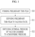
- FIG. 1 is a flow chart for describing a method of preparing single crystal perovskite according to an exemplary embodiment of the present invention.
- a method of producing a perovskite thin film includes: forming a preliminary thin film by applying a perovskite precursor solution containing an alkylamine ligand on a substrate (S10); exposing the preliminary thin film to a vacuum state by transferring the preliminary thin film to a vacuum chamber (S11); and switching an internal pressure of the vacuum chamber to an atmospheric pressure (S12).
- a perovskite photoactive precursor solution is prepared, an additive is injected into the prepared solution, and stirring is performed for 5 minutes or longer.
- the perovskite precursor solution may form ABX 3 , which is a perovskite structure, in which A may be an organic/inorganic cation (methylammonium (CH 3 NH 3 + , MA + ), formamidinium (HC(NH 2 ) 2 + , FA + ), cesium (Cs), rubidium (Rb), or the like), B may be a divalent metal cation (Pb 2+ , Sn 2+ , or the like), and X may be a halogen anion (Cl - , Br - , I - , or the like).
- A may be an organic/inorganic cation (methylammonium (CH 3 NH 3 + , MA + ), formamidinium (HC(NH 2 ) 2 + , FA + ), cesium (Cs), rubidium (Rb), or the like)
- B may be a divalent metal cation (Pb 2+ , Sn 2+ , or the like)
- the additive may be added in an amount of 0.001 wt% to 10 wt%, and may include a substituted or unsubstituted C1 to C30 aliphatic ammonium salt, a substituted or unsubstituted C6 to C30 aromatic ammonium salt, a substituted or unsubstituted C1 to C30 aliphatic amine salt, a substituted or unsubstituted C6 to C30 aromatic amine salt, or a combination thereof.
- substituted or unsubstituted C1 to C30 aliphatic ammonium salt or the substituted or unsubstituted C6 to C30 aromatic ammonium salt may be any one of 2-chloroethylammonium (CIEA + ), ethane-1,2-diammonium (EDA 2+ ), 2-(methylthio)-ethylammonium (MTEA + ), n-propylammonium (n-PA + ), n-butylammonium (n-BA + ), iso-butylammonium (i-BA + ), tert-butylammonium (tBA + ), tetra-butylammonium (TBA + ), 5-ammonium valeric acid (5-AVA + ), n-hexyl trimethyl ammonium (HTAB + ), n-octylammonium (n-OA + ), n-dodecylammonium (n
- the additive may further contain a passivation additive.
- a metal cation K + , Na + , or the like
- the preliminary thin film may be a wet film formed by a method such as a spin coating method, a slot-die coating method, or an inkjet coating method.
- the preliminary thin film In the exposing of the preliminary thin film to the vacuum state (S11), the preliminary thin film is transferred to the vacuum chamber, and then the preliminary thin film is exposed to a vacuum state in the vacuum chamber for 1 second to 10 minutes.
- the vacuum state of the vacuum chamber is switched to an atmospheric state, and an inert gas such as nitrogen (N 2 ) or argon (Ar) gas is injected to switch the vacuum state of the vacuum chamber to the atmospheric state.
- an inert gas such as nitrogen (N 2 ) or argon (Ar) gas
- the inert gas may be injected into the vacuum chamber in a state of being heated at 25°C to 300°C.
- a perovskite precursor solution was prepared.
- the substrate was a glass substrate, and a size of the substrate was 2.5 ⁇ 2.5 cm 2 .
- the spin coating was performed at 500 rpm for 5 seconds and then was performed at 5,000 rpm for 45 seconds.
- the spin-coated substrate was subjected to a heat treatment by using a hot plate at 100°C for 10 minutes to form a perovskite thin film.
- a perovskite thin film of Comparative Example 2 was formed in the same manner as that of Comparative Example 1, except that the process of applying CB as an anti-solvent was not performed.
- the precursor solution was applied onto a substrate by spin coating in the same manner as that of Comparative Example 1 to form a preliminary thin film.
- the preliminary thin film was transferred to a vacuum chamber, the inside of the chamber was switched to a vacuum state at 1 -1 to 3 -3 torr, nitrogen gas heated to 100°C was injected, and the internal state of the vacuum chamber was switched to an atmospheric state, thereby forming a perovskite thin film.
- a perovskite thin film of Experimental Example 2 was formed in the same manner as that of Experimental Example 1, except that 1 mg of octylammonium iodine was added as an additive and stirring was performed for 1 hour or longer.
- a perovskite thin film of Comparative Example 3 was formed in the same manner as that of Experimental Example 1, except that the process of applying CB as an anti-solvent was performed.
- FIG. 2 is X-ray diffraction data of the perovskite thin film according to Comparative Example 1
- FIGS. 3 and 4 are X-ray diffraction data of the perovskite thin films according to Experimental Examples 1 and 2.
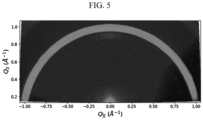
- FIGS. 5 and 6 are grazing-incidence wide-angle X-ray scattering (GIWAXS) photographs of the perovskite thin films according to Comparative Example 1 and Experimental Example 1, respectively.
- GIWAXS grazing-incidence wide-angle X-ray scattering
- FIGS. 7 and 8 are X-ray diffraction data of the perovskite thin films according to Comparative Examples 2 and 3.
- Comparative Example 3 oleylamine was contained as in Experimental Example 1, whereas a process of applying an anti-solvent was performed, and it could be confirmed that polycrystalline characteristics were exhibited in a case where the process of applying an anti-solvent was performed even when oleylamine was contained.
- a single crystal perovskite thin film was produced only by performing the switching process including a vacuum and heat treatment after coating with a precursor solution containing an additive.
- the perovskite thin film may be used as a photoactive layer of a solar cell.
- FIG. 9 is a schematic cross-sectional view of a solar cell according to an exemplary embodiment of the present invention.
- the solar cell includes: a substrate 610, a first electrode 620 formed on the substrate 610; a hole transport layer 630 formed on the first electrode 620; a photoactive layer 640 formed on the hole transport layer 630; an electron transport layer 650 formed on the photoactive layer 640; and a second electrode 660 formed on the electron transport layer 650.
- the substrate 610 is formed of glass, which is a transparent material
- the first electrode 620 is formed of a transparent material, and may be formed of, for example, indium tin oxide (ITO), indium zinc oxide (IZO), or the like.
- the hole transport layer 630 may include a first hole transport layer 61 and a second hole transport layer 62 formed on the first hole transport layer 61.
- the first hole transport layer 61 may be formed by performing sputtering, thermal evaporation, slot die, spin coating, or the like of NiOx
- the second hole transport layer 62 may be formed by coating any one of MEO-2PACz and PTAA and then performing a heat treatment.
- the photoactive layer 640 may be a perovskite thin film formed by a method of producing a single crystal perovskite thin film according to an exemplary embodiment of the present invention.
- a passivation layer may be formed on a surface of the photoactive layer 640 for passivation, and may include, for example, any one of LiF, KF, FAI, FABr Csl, CsBr, MAl, MABr, and Rbl.
- the passivation layer may be formed at a thickness of 0.1 nm to 3 nm, and may be formed by a method such as a thermal evaporation method, a spin coating method, a dip coating method, a drop casting method, a slot die coating method, a blade coating method, a meniscus coating method, a gravure printing method, a screen printing method, a spray coating method, a 3D direct ink writing method, or an inkjet printing method.
- the electron transport layer 650 may include a first electron transport layer 63 and a second electron transport layer 64, the first electron transport layer 63 may be formed by depositing C60, and the second electron transport layer 64 may be formed by using SnOx at a thickness of 5 nm to 30 nm using an atomic layer deposition reactor.
- an operation temperature of the atomic layer deposition reactor is 70°C to 150°C.
- the second electrode 660 may include a transparent electrode formed of ITO or IZO, a metal such as Cu, Ag, or Al, an alloy thereof, or a plurality of layers including the same.
- An ITO transparent electrode was deposited on a transparent glass substrate, and NiOx was deposited on the transparent electrode at a thickness of 10 nm by a sputtering method.
- the photoactive layer was transferred to a thermal evaporator to deposit LiF at a thickness of 1 nm or less by thermal evaporation so as to perform surface passivation, and then, C60 was deposited at a thickness of 12 nm through thermal evaporation, thereby forming a lower electron transport layer. Then, SnOx was deposited by a thermal evaporation or atomic layer deposition (ALD) process at a thickness of 10 nm to form an upper electron transport layer.
- ALD atomic layer deposition
- Silver (Ag) was thermally evaporated on the electron transport layer to manufacture a solar cell including a metal electrode.
- a solar cell was manufactured in the same manner as that of Experimental Example 3, except that a photoactive layer formed of a perovskite thin film was formed in the same manner as that of Comparative Example 1.
- a solar cell was manufactured in the same manner as that of Experimental Example 3, and a photoactive layer was formed in the same manner as that of Experimental Example 1 except for injecting nitrogen gas heated to 80°C into a vacuum chamber.
- a solar cell was manufactured in the same manner as that of Experimental Example 3, and a photoactive layer was formed in the same manner as that of Experimental Example 1 except for injecting nitrogen gas heated to 20°C into a vacuum chamber.
- a solar cell was manufactured in the same manner as that of Experimental Example 3, and a photoactive layer was formed in the same manner as that of Experimental Example 1 except for using a precursor solution further containing 1 mg/ml of potassium iodide (Kl) as a passivation additive.
- Kl potassium iodide
- a solar cell was manufactured in the same manner as that of Experimental Example 3, and a photoactive layer was formed in the same manner as that of Experimental Example 1 except for using a precursor solution further containing 1 mg of BASCN as a passivation additive.
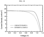
- FIG. 10 is a voltage-current graph of the solar cells manufactured according to Experimental Example 3 and Comparative Example 4.
- Table 1 V oc [V] J sc [mA cm- 2 ] FF [%] PCE [%] Comparative Example 4 1.072 22.77 60.84 14.85 Experimental Example 3 1.113 22.48 75.63 18.93
- FIG. 11 is a graph showing efficiency of the solar cells manufactured according to Experimental Example 4 and Comparative Example 5.
- FIG. 12 is a graph showing efficiency of the solar cells manufactured according to Experimental Examples 3 and 5.
- Iodine and metal cations (K + ) of potassium may form ionic defects with uncoordinated anions. Since the perovskite photoactive layer generally has uncoordinated halogen ions and antisite defects, the metal cations (K + ) contained in the precursor solution may increase the efficiency by effectively passivating electron-rich defects and suppressing the oxidation reaction of halogen ions to reduce non-radiative recombination.
- FIG. 13 is a graph showing efficiency of the solar cells manufactured according to Experimental Examples 3 and 6.
- Thiocyanate (SCN - ) of benzylammonium thiocyanate may passivate defects such as Pb 2+ in the perovskite photoactive layer, and at the same time, benzylammonium (BA + ) may form BAPbl 3 . Therefore, the efficiency may be further improved by such a synergy effect.
- defects may exist in the single crystal perovskite photoactive layer according to the present invention. These defects may lead to non-radiative charge carrier recombination, which may cause deterioration of the efficiency.
- crystallization of perovskite may be controlled, a band energy level may be optimized, the defects may be passivated, and a charge carrier mobility rate may be affected.
- the efficiency of the solar cell may be improved by forming a photoactive layer using the single crystal perovskite thin film, and a solar cell having further improved efficiency may be manufactured by adding a passivation additive to a precursor solution.
Landscapes
- Chemical & Material Sciences (AREA)
- Engineering & Computer Science (AREA)
- Materials Engineering (AREA)
- Crystallography & Structural Chemistry (AREA)
- Metallurgy (AREA)
- Organic Chemistry (AREA)
- Inorganic Chemistry (AREA)
- Physics & Mathematics (AREA)
- Electromagnetism (AREA)
- Manufacturing & Machinery (AREA)
- Chemical Kinetics & Catalysis (AREA)
- General Chemical & Material Sciences (AREA)
- Photovoltaic Devices (AREA)
- Spectroscopy & Molecular Physics (AREA)
Abstract
Description
- This application claims priority to and the benefit of
Korean Patent Application No. 10-2022-0056793 filed in the Korean Intellectual Property Office on May 09, 2022 - The present invention relates to a method of preparing single crystal perovskite, and more particularly, to a method of preparing single crystal perovskite used in a solar cell and a method of manufacturing a solar cell using single crystal perovskite.
- Recently, an organic-inorganic hybrid perovskite (OIHP) solar cell using a perovskite material (ABX3 having a structure in which A is a monovalent organic/inorganic methylammonium (CH3NH3 +, MA+) or formamidinium (HC(NH2)2 +, FA+), B is a divalent metal cation Pb2+ or Sn2+, and X is a halogen anion Cl-, Br-, or I-) for a photoactive layer has shown a rapid increase in power conversion efficiency (PCE) from 3.8% in 2009 to 25.5% in 2021.
- The high photoelectric conversion efficiency of the perovskite-based solar cell is based on excellent photoelectric properties of an organic-inorganic hybrid perovskite photoactive layer such as a high charge carrier mobility, a long intrinsic carrier recombination lifetime, a simply tunable band gap, long electron and hole diffusion lengths, and a high absorption coefficient in visible light range, and the perovskite-based solar cell is attracting considerable attention as a next-generation solar cell to replace a silicon solar cell and an alternative energy source in the future.
- However, the solar cell including the perovskite photoactive layer is mainly formed of polycrystalline perovskite that is relatively easily prepared. Such polycrystalline perovskite is relatively less efficient than single crystal perovskite due to a high trap density. In addition, the efficiency of the polycrystalline perovskite solar cell is stagnant recently due to a high density of fundamental structural defects (for example, point defects, grain boundaries, and the like).
- In comparison, it is known that a trap density of a single crystal perovskite photoactive layer is tens of times lower than that of a polycrystalline perovskite photoactive layer, such that a diffusion length of carriers is approximately 100 times longer than that of the polycrystalline perovskite photoactive layer. Therefore, the single crystal perovskite photoactive layer may exhibit performance beyond the limit of the polycrystalline perovskite photoactive layer, but a process time in a method of preparing single crystal perovskite according to the related art takes from several hours to a week, and an apparatus for preparing single crystal perovskite is significantly complicated. Therefore, the single crystal perovskite has not been applied to a solar cell.
- The above information disclosed in this Background section is only for enhancement of understanding of the background of the invention, and therefore it may contain information that does not form the prior art that is already known in this country to a person of ordinary skill in the art.
- The present invention has been made in an effort to provide a method of preparing single crystal perovskite and a method of manufacturing a solar cell using single crystal perovskite by solving the problem of a long time required for a method of preparing single crystal perovskite and complexity of an apparatus of preparing single crystal perovskite according to the related art.
- Further, the present invention has been made in an effort to provide an environmentally friendly method of preparing single crystal perovskite by eliminating a process using an anti-solvent that is most widely used in the method of preparing perovskite according to the related art.
- An exemplary embodiment of the present invention provides a method of forming single crystal perovskite, the method including: forming a preliminary thin film by applying a perovskite precursor solution containing an additive on a substrate; exposing the preliminary thin film to a vacuum state by transferring the preliminary thin film to a vacuum chamber; and switching an internal pressure of the vacuum chamber to an atmospheric pressure, wherein the additive includes a substituted or unsubstituted C1 to C30 aliphatic ammonium salt, a substituted or unsubstituted C6 to C30 aromatic ammonium salt, a substituted or unsubstituted C1 to C30 aliphatic amine salt, a substituted or unsubstituted C6 to C30 aromatic amine salt, or a combination thereof.
- The substituted or unsubstituted C1 to C30 aliphatic ammonium salt or the substituted or unsubstituted C6 to C30 aromatic ammonium salt may be any one of 2-chloroethylammonium (CIEA+), ethane-1,2-diammonium (EDA2+), 2-(methylthio)-ethylammonium (MTEA+), n-propylammonium (n-PA+), n-butylammonium (n-BA+), iso-butylammonium (i-BA+), tert-butylammonium (tBA+), tetra-butylammonium (TBA+), 5-ammonium valeric acid (5-AVA+), n-hexyl trimethyl ammonium (HTAB+), n-octylammonium (n-OA+), n-dodecylammonium (n-DA+), phenethylammonium (PEA+), pentafluorophenylethylammonium (FEA+), 4-tert-butyl-benzylammonium (tBBA+), 1-napthylmethylammonium (NMA+), and 2-thiophene ethylammonium (2-TEA+).
- The substituted or unsubstituted C1 to C30 aliphatic amine salt or the substituted or unsubstituted C6 to C30 aromatic amine salt may be oleylamine (OAm+) or S-benzyl-L-cysteine (SBLC+).
- The exposing of the preliminary thin film to the vacuum state may be performed for 1 second to 10 minutes.
- A vacuum pressure may be 1-1 to 3-3 torr.
- In the switching of the internal pressure of the vacuum chamber to the atmospheric pressure, an inert gas may be injected into the vacuum chamber.
- The inert gas may be nitrogen or argon.
- The inert gas may be injected by being heated at 25°C to 300°C.
- The additive may be injected in an amount of 0.001 wt% to 10 wt% with respect to the amount of the perovskite precursor solution.
- The perovskite precursor solution may further contain a passivation additive, and the passivation additive may have at least one functional group of a metal cation (K+ or Na+), -SCN, -CN, -NH2, -N3, -CI, -Br, -I, -F, -COOH, - POOH, -OH, -CF3, -OCH3, -C=O, -S=O, -SH, -NH, a benzyl group, an alkoxy group, and -CH3.
- The passivation additive may be potassium iodide or benzylammonium thiocyanate (BASCN).
- Another exemplary embodiment of the present invention provides a method of manufacturing a solar cell, the method including: forming a first electrode on a substrate; forming a hole transport layer on the first electrode; forming a photoactive layer on the hole transport layer; forming an electron transport layer on the photoactive layer; and forming a second electrode on the electron transport layer, wherein the forming of the photoactive layer includes: forming a preliminary thin film by applying a perovskite precursor solution containing an additive on the hole transport layer; exposing the preliminary thin film to a vacuum state by transferring the preliminary thin film to a vacuum chamber; and switching an internal pressure of the vacuum chamber to an atmospheric pressure, and the additive includes a substituted or unsubstituted C1 to C30 aliphatic ammonium salt, a substituted or unsubstituted C6 to C30 aromatic ammonium salt, a substituted or unsubstituted C1 to C30 aliphatic amine salt, a substituted or unsubstituted C6 to C30 aromatic amine salt, or a combination thereof.
- The substituted or unsubstituted C1 to C30 aliphatic ammonium salt or the substituted or unsubstituted C6 to C30 aromatic ammonium salt may be any one of 2-chloroethylammonium (CIEA+), ethane-1,2-diammonium (EDA2+), 2-(methylthio)-ethylammonium (MTEA+), n-propylammonium (n-PA+), n-butylammonium (n-BA+), iso-butylammonium (i-BA+), tert-butylammonium (tBA+), tetra-butylammonium (TBA+), 5-ammonium valeric acid (5-AVA+), n-hexyl trimethyl ammonium (HTAB+), n-octylammonium (n-OA+), n-dodecylammonium (n-DA+), phenethylammonium (PEA+), pentafluorophenylethylammonium (FEA+), 4-tert-butyl-benzylammonium (tBBA+), 1-napthylmethylammonium (NMA+), and 2-thiophene ethylammonium (2-TEA+).
- The substituted or unsubstituted C1 to C30 aliphatic amine salt or the substituted or unsubstituted C6 to C30 aromatic amine salt may be oleylamine (OAm+) or S-benzyl-L-cysteine (SBLC+).
- The exposing of the preliminary thin film to the vacuum state may be performed for 1 second to 10 minutes.
- In the switching of the internal pressure of the vacuum chamber to the atmospheric pressure, an inert gas may be injected into the vacuum chamber.
- The inert gas may be injected by being heated at 25°C to 300°C.
- The additive may be injected in an amount of 0.001 wt% to 10 wt% with respect to the amount of the perovskite precursor solution.
- The perovskite precursor solution may further contain a passivation additive, and the passivation additive may have at least one functional group of a metal cation (K+ or Na+), -SCN, -CN, -NH2, -N3, -CI, -Br, -I, -F, -COOH, - POOH, -OH, -CF3, -OCH3, -C=O, -S=O, -SH, -NH, a benzyl group, an alkoxy group, and -CH3.
- As set forth above, according to an exemplary embodiment of the present invention, single crystal perovskite may be easily prepared by adding the additive to the perovskite precursor solution and performing the vacuum process. Therefore, the process time may be reduced compared to the method of preparing single crystal perovskite according to the related art, and an apparatus for preparing single crystal perovskite may be simplified to improve productivity.
- Further, single crystal perovskite may be prepared without using an anti-solvent, such that it is possible to provide an environmentally friendly method of preparing single crystal perovskite.
- Further, the solar cell including single crystal perovskite is manufactured, such that a solar cell having improved efficiency may be provided.
-
-
FIG. 1 is a flow chart for describing a method of preparing single crystal perovskite according to an exemplary embodiment of the present invention. -
FIG. 2 is X-ray diffraction data of a perovskite thin film according to Comparative Example 1. -
FIGS. 3 and4 are X-ray diffraction data of perovskite thin films according to Experimental Examples 1 and 2. -
FIGS. 5 and6 are grazing-incidence wide-angle X-ray scattering (GIWAXS) photographs of the perovskite thin films according to Comparative Example 1 and Experimental Example 1, respectively. -
FIGS. 7 and8 are X-ray diffraction data of perovskite thin films according to Comparative Examples 2 and 3. -
FIG. 9 is a schematic cross-sectional view of a solar cell according to an exemplary embodiment of the present invention. -
FIG. 10 is a voltage-current graph of solar cells manufactured according to Experimental Example 3 and Comparative Example 4. -
FIG. 11 is a graph showing efficiency of solar cells manufactured according to Experimental Example 4 and Comparative Example 5. -
FIG. 12 is a graph showing efficiency of solar cells manufactured according to Experimental Examples 3 and 5. -
FIG. 13 is a graph showing efficiency of solar cells manufactured according to Experimental Examples 3 and 6. - Hereinafter, exemplary embodiments of the present invention will be described in detail with reference to the accompanying drawings so that those skilled in the art may easily practice the present invention. However, the present invention may be implemented in various different forms and is not limited to exemplary embodiments described herein.
- In addition, throughout the present specification, unless explicitly described to the contrary, "comprising" any components will be understood to imply the inclusion of other components rather than the exclusion of any other components.
-
FIG. 1 is a flow chart for describing a method of preparing single crystal perovskite according to an exemplary embodiment of the present invention. - As illustrated in
FIG. 1 , a method of producing a perovskite thin film according to an exemplary embodiment of the present invention includes: forming a preliminary thin film by applying a perovskite precursor solution containing an alkylamine ligand on a substrate (S10); exposing the preliminary thin film to a vacuum state by transferring the preliminary thin film to a vacuum chamber (S11); and switching an internal pressure of the vacuum chamber to an atmospheric pressure (S12). - In the forming of the preliminary thin film (S10), a perovskite photoactive precursor solution is prepared, an additive is injected into the prepared solution, and stirring is performed for 5 minutes or longer.
- The perovskite precursor solution may form ABX3, which is a perovskite structure, in which A may be an organic/inorganic cation (methylammonium (CH3NH3 +, MA+), formamidinium (HC(NH2)2 +, FA+), cesium (Cs), rubidium (Rb), or the like), B may be a divalent metal cation (Pb2+, Sn2+, or the like), and X may be a halogen anion (Cl-, Br-, I-, or the like).
- The additive may be added in an amount of 0.001 wt% to 10 wt%, and may include a substituted or unsubstituted C1 to C30 aliphatic ammonium salt, a substituted or unsubstituted C6 to C30 aromatic ammonium salt, a substituted or unsubstituted C1 to C30 aliphatic amine salt, a substituted or unsubstituted C6 to C30 aromatic amine salt, or a combination thereof. For example, substituted or unsubstituted C1 to C30 aliphatic ammonium salt or the substituted or unsubstituted C6 to C30 aromatic ammonium salt may be any one of 2-chloroethylammonium (CIEA+), ethane-1,2-diammonium (EDA2+), 2-(methylthio)-ethylammonium (MTEA+), n-propylammonium (n-PA+), n-butylammonium (n-BA+), iso-butylammonium (i-BA+), tert-butylammonium (tBA+), tetra-butylammonium (TBA+), 5-ammonium valeric acid (5-AVA+), n-hexyl trimethyl ammonium (HTAB+), n-octylammonium (n-OA+), n-dodecylammonium (n-DA+), phenethylammonium (PEA+), pentafluorophenylethylammonium (FEA+), 4-tert-butyl-benzylammonium (tBBA+), 1-napthylmethylammonium (NMA+), and 2-thiophene ethylammonium (2-TEA+), and the substituted or unsubstituted C1 to C30 aliphatic amine salt or the substituted or unsubstituted C6 to C30 aromatic amine salt may be oleylamine (OAm+) or S-benzyl-L-cysteine (SBLC+).
- The additive may further contain a passivation additive.
- The passivation additive may have at least one functional group of a metal cation (K+, Na+, or the like), -SCN, -CN, -NH2, -N3, -CI, -Br, -I, -F, -COOH, -POOH, -OH, -CF3, -OCH3, -C=O, -S=O, -SH, -NH, a benzyl group, an alkoxy group, and -CH3.
- The preliminary thin film may be a wet film formed by a method such as a spin coating method, a slot-die coating method, or an inkjet coating method.
- In the exposing of the preliminary thin film to the vacuum state (S11), the preliminary thin film is transferred to the vacuum chamber, and then the preliminary thin film is exposed to a vacuum state in the vacuum chamber for 1 second to 10 minutes.
- In the switching of the internal pressure of the vacuum chamber to the atmospheric pressure (S12), the vacuum state of the vacuum chamber is switched to an atmospheric state, and an inert gas such as nitrogen (N2) or argon (Ar) gas is injected to switch the vacuum state of the vacuum chamber to the atmospheric state. As a result, a single crystal perovskite thin film is formed. In this case, the inert gas may be injected into the vacuum chamber in a state of being heated at 25°C to 300°C.
- A perovskite precursor solution was prepared. The perovskite precursor solution was prepared by adding 65.94 mg of Csl, 187.02 mg of FAI, 13.59 mg of FABr, 573 mg of Pbl2, and 79.82 mg of PbBr2 were added to 1 ml of a solvent (DMF:DMSO = 9:1), and stirring the solution for 3 hours or longer.
- Thereafter, 90 ul of the perovskite precursor solution was applied onto a substrate by a spin coating method to form a preliminary thin film. The substrate was a glass substrate, and a size of the substrate was 2.5 × 2.5 cm2. The spin coating was performed at 500 rpm for 5 seconds and then was performed at 5,000 rpm for 45 seconds.
- Thereafter, 30 seconds before the spin coating was completed, 300 ul of an anti-solvent solution CB (chlorobenzene) was applied to a surface of the preliminary thin film.
- Then, the spin-coated substrate was subjected to a heat treatment by using a hot plate at 100°C for 10 minutes to form a perovskite thin film.
- A perovskite thin film of Comparative Example 2 was formed in the same manner as that of Comparative Example 1, except that the process of applying CB as an anti-solvent was not performed.
- The same precursor solution as in Comparative Example 1 was prepared, 1.4 ul of oleylamine as an additive was added to the prepared precursor solution, and the solution was stirred for 20 minutes or longer, thereby preparing a precursor solution.
- Thereafter, the precursor solution was applied onto a substrate by spin coating in the same manner as that of Comparative Example 1 to form a preliminary thin film.
- Then, the preliminary thin film was transferred to a vacuum chamber, the inside of the chamber was switched to a vacuum state at 1-1 to 3-3 torr, nitrogen gas heated to 100°C was injected, and the internal state of the vacuum chamber was switched to an atmospheric state, thereby forming a perovskite thin film.
- A perovskite thin film of Experimental Example 2 was formed in the same manner as that of Experimental Example 1, except that 1 mg of octylammonium iodine was added as an additive and stirring was performed for 1 hour or longer.
- A perovskite thin film of Comparative Example 3 was formed in the same manner as that of Experimental Example 1, except that the process of applying CB as an anti-solvent was performed.
-
FIG. 2 is X-ray diffraction data of the perovskite thin film according to Comparative Example 1, andFIGS. 3 and4 are X-ray diffraction data of the perovskite thin films according to Experimental Examples 1 and 2. - Referring to
FIG. 2 according to Comparative Example 1 according to the related art, in the perovskite thin film, it could be confirmed that (100), (110), (111), and (200) crystal planes in several directions, that is, polycrystals appeared. - On the other hand, referring to
FIGS. 3 and4 according to Experimental Examples 1 and 2, it could be confirmed that (110) and (111) crystal planes did not appear, and only (100) and (200) single crystal planes in a vertical direction appeared. -
FIGS. 5 and6 are grazing-incidence wide-angle X-ray scattering (GIWAXS) photographs of the perovskite thin films according to Comparative Example 1 and Experimental Example 1, respectively. - Referring to
FIG. 5 according to Comparative Example 1, a ring form, which was a characteristic of a polycrystalline structure, was confirmed in a reciprocal lattice space. On the other hand, referring toFIG. 6 according to Experimental Example 1, a single crystal spot form was confirmed. -
FIGS. 7 and8 are X-ray diffraction data of the perovskite thin films according to Comparative Examples 2 and 3. - Referring to
FIG. 7 according to Comparative Example 2, in the perovskite thin film, it could be confirmed that (100), (110), and (111) crystal planes in several directions, that is, polycrystals appeared. - Unlike Experimental Example 1, in Comparative Example 1, the process of applying the anti-solvent was not performed, oleylamine as an additive was not contained, and it was confirmed that the growth of single crystals was promoted by oleylamine.
- Referring to
FIG. 8 according to Comparative Example 3, in the perovskite thin film, it could be confirmed that (100), (110), (111), and (200) crystal planes in several directions, that is, polycrystals appeared. - In Comparative Example 3, oleylamine was contained as in Experimental Example 1, whereas a process of applying an anti-solvent was performed, and it could be confirmed that polycrystalline characteristics were exhibited in a case where the process of applying an anti-solvent was performed even when oleylamine was contained.
- That is, as in an exemplary embodiment of the present invention, it could be confirmed that a single crystal perovskite thin film was produced only by performing the switching process including a vacuum and heat treatment after coating with a precursor solution containing an additive.
- The perovskite thin film may be used as a photoactive layer of a solar cell.
- Hereinafter, the solar cell according to an exemplary embodiment of the present invention will be described in detail with reference to the accompanying drawings.
-
FIG. 9 is a schematic cross-sectional view of a solar cell according to an exemplary embodiment of the present invention. - Referring to
FIG. 9 , the solar cell according to an exemplary embodiment of the present invention includes: asubstrate 610, afirst electrode 620 formed on thesubstrate 610; ahole transport layer 630 formed on thefirst electrode 620; aphotoactive layer 640 formed on thehole transport layer 630; an electron transport layer 650 formed on thephotoactive layer 640; and asecond electrode 660 formed on the electron transport layer 650. - The
substrate 610 is formed of glass, which is a transparent material, and thefirst electrode 620 is formed of a transparent material, and may be formed of, for example, indium tin oxide (ITO), indium zinc oxide (IZO), or the like. - The
hole transport layer 630 may include a first hole transport layer 61 and a secondhole transport layer 62 formed on the first hole transport layer 61. The first hole transport layer 61 may be formed by performing sputtering, thermal evaporation, slot die, spin coating, or the like of NiOx, and the secondhole transport layer 62 may be formed by coating any one of MEO-2PACz and PTAA and then performing a heat treatment. - The
photoactive layer 640 may be a perovskite thin film formed by a method of producing a single crystal perovskite thin film according to an exemplary embodiment of the present invention. - A passivation layer may be formed on a surface of the
photoactive layer 640 for passivation, and may include, for example, any one of LiF, KF, FAI, FABr Csl, CsBr, MAl, MABr, and Rbl. The passivation layer may be formed at a thickness of 0.1 nm to 3 nm, and may be formed by a method such as a thermal evaporation method, a spin coating method, a dip coating method, a drop casting method, a slot die coating method, a blade coating method, a meniscus coating method, a gravure printing method, a screen printing method, a spray coating method, a 3D direct ink writing method, or an inkjet printing method. - The electron transport layer 650 may include a first
electron transport layer 63 and a second electron transport layer 64, the firstelectron transport layer 63 may be formed by depositing C60, and the second electron transport layer 64 may be formed by using SnOx at a thickness of 5 nm to 30 nm using an atomic layer deposition reactor. In this case, an operation temperature of the atomic layer deposition reactor is 70°C to 150°C. - The
second electrode 660 may include a transparent electrode formed of ITO or IZO, a metal such as Cu, Ag, or Al, an alloy thereof, or a plurality of layers including the same. - An ITO transparent electrode was deposited on a transparent glass substrate, and NiOx was deposited on the transparent electrode at a thickness of 10 nm by a sputtering method.
- Thereafter, a heat treatment was performed at 300°C for 10 minutes, 90 ul of MEO-2PACz (SAM material) dissolved in ethanol at a concentration of 3 mM was applied onto NiOx, and 10 after seconds, spin coating was performed at 3,000 rpm for 20 seconds. Thereafter, a heat treatment was performed on a hot plate at 100°C for 10 minutes to form a hole transport layer (carrier transport layer).
- Then, a photoactive layer formed of a single crystal perovskite thin film was formed on the hole transport layer in the same manner as that of Experimental Example 1.
- Thereafter, the photoactive layer was transferred to a thermal evaporator to deposit LiF at a thickness of 1 nm or less by thermal evaporation so as to perform surface passivation, and then, C60 was deposited at a thickness of 12 nm through thermal evaporation, thereby forming a lower electron transport layer. Then, SnOx was deposited by a thermal evaporation or atomic layer deposition (ALD) process at a thickness of 10 nm to form an upper electron transport layer.
- Silver (Ag) was thermally evaporated on the electron transport layer to manufacture a solar cell including a metal electrode.
- A solar cell was manufactured in the same manner as that of Experimental Example 3, except that a photoactive layer formed of a perovskite thin film was formed in the same manner as that of Comparative Example 1.
- A solar cell was manufactured in the same manner as that of Experimental Example 3, and a photoactive layer was formed in the same manner as that of Experimental Example 1 except for injecting nitrogen gas heated to 80°C into a vacuum chamber.
- A solar cell was manufactured in the same manner as that of Experimental Example 3, and a photoactive layer was formed in the same manner as that of Experimental Example 1 except for injecting nitrogen gas heated to 20°C into a vacuum chamber.
- A solar cell was manufactured in the same manner as that of Experimental Example 3, and a photoactive layer was formed in the same manner as that of Experimental Example 1 except for using a precursor solution further containing 1 mg/ml of potassium iodide (Kl) as a passivation additive.
- A solar cell was manufactured in the same manner as that of Experimental Example 3, and a photoactive layer was formed in the same manner as that of Experimental Example 1 except for using a precursor solution further containing 1 mg of BASCN as a passivation additive.
-
FIG. 10 is a voltage-current graph of the solar cells manufactured according to Experimental Example 3 and Comparative Example 4.[Table 1] Voc [V] Jsc [mA cm-2] FF [%] PCE [%] Comparative Example 4 1.072 22.77 60.84 14.85 Experimental Example 3 1.113 22.48 75.63 18.93 - Referring to
FIG. 10 and Table 1, it could be confirmed that a voltage-to-current density of the solar cell manufactured according to Experimental Example 3 was higher than a voltage-to-current density of the solar cell manufactured according to Comparative Example 4. Therefore, it could be confirmed that the efficiency of the solar cell manufactured according to Experimental Example 3 was 18.93%, whereas the efficiency of the solar cell manufactured according to Comparative Example 4 was 14.85%, which was low. - It could be confirmed that the efficiency of the solar cell of Experimental Example 3 was relatively higher than that of the solar cell of Comparative Example 4 because a trap density of the photoactive layer formed of the single crystal perovskite thin film of the solar cell according to Experimental Example 3 was lower than that of the photoactive layer formed of the polycrystalline perovskite thin film of the solar cell of Comparative Example 4.
-
FIG. 11 is a graph showing efficiency of the solar cells manufactured according to Experimental Example 4 and Comparative Example 5.[Table 2] Voc [V] Jsc [mA cm-2] FF [%] PCE [%] Comparative Example 5 1.058 21.94 77.11 17.89 Experimental Example 4 1.102 22.46 77.07 19.08 - Referring to
FIG. 11 and Table 2, it could be confirmed that a voltage-to-current density of the solar cell manufactured according to Experimental Example 4 was higher than a voltage-to-current density of the solar cell manufactured according to Comparative Example 5. Therefore, it could be confirmed that the efficiency of the solar cell manufactured according to Comparative Example 5 was 17.89%, which was low, whereas the efficiency of the solar cell manufactured according to Experimental Example 4 was 19.8%, which was high. -
FIG. 12 is a graph showing efficiency of the solar cells manufactured according to Experimental Examples 3 and 5.[Table 3] Voc [V] Jsc [mA cm-2] FF [%] PCE [%] Experimental Example 3 1.063 22.47 76.07 18.17 Experimental Example 5 1.075 22.64 79.21 19.29 - Referring to
FIG. 12 and Table 3, it could be confirmed that the efficiency of the solar cell manufactured by adding potassium iodide (KI) to the precursor solution for passivation as in Experimental Example 5 was higher than that of the solar cell of Experimental Example 3 in which potassium iodide was not added. Therefore, it could be confirmed that the efficiency of the solar cell of Experimental Example 3 was 18.17%, whereas the efficiency of the solar cell of Experimental Example 5 was 19.29%, which was high. - Iodine and metal cations (K+) of potassium may form ionic defects with uncoordinated anions. Since the perovskite photoactive layer generally has uncoordinated halogen ions and antisite defects, the metal cations (K+) contained in the precursor solution may increase the efficiency by effectively passivating electron-rich defects and suppressing the oxidation reaction of halogen ions to reduce non-radiative recombination.
-
FIG. 13 is a graph showing efficiency of the solar cells manufactured according to Experimental Examples 3 and 6.[Table 4] Voc [V] Jsc [mA cm-2] FF [%] PCE [%] Experimental Example 3 1.063 22.47 76.07 18.17 Experimental Example 6 1.075 22.64 79.21 19.29 - Referring to
FIG. 13 and Table 4, it could be confirmed that a voltage-to-current density of the solar cell manufactured by adding benzylammonium thiocyanate (BASCN) to the precursor solution for passivation as in Experimental Example 6 was higher than that of the solar cell according to Experimental Example 3. Therefore, it could be confirmed that the efficiency of the solar cell according to Experimental Example 3 was 18.17%, whereas the efficiency of the solar cell according to Experimental Example 6 was increased to 19.29%. - Thiocyanate (SCN-) of benzylammonium thiocyanate may passivate defects such as Pb2+ in the perovskite photoactive layer, and at the same time, benzylammonium (BA+) may form BAPbl3. Therefore, the efficiency may be further improved by such a synergy effect.
- Several types of defects may exist in the single crystal perovskite photoactive layer according to the present invention. These defects may lead to non-radiative charge carrier recombination, which may cause deterioration of the efficiency.
- Therefore, when an additive effective in the passivation of the defects is introduced, crystallization of perovskite may be controlled, a band energy level may be optimized, the defects may be passivated, and a charge carrier mobility rate may be affected.
- As set forth above, in the present invention, the efficiency of the solar cell may be improved by forming a photoactive layer using the single crystal perovskite thin film, and a solar cell having further improved efficiency may be manufactured by adding a passivation additive to a precursor solution.
- Although the exemplary embodiments of the present invention have been described hereinabove, the present invention is not limited thereto, and various modifications may be made within the scope of the claims, the detailed description of the invention, and the accompanying drawings.
Claims (15)
- A method of forming single crystal perovskite, the method comprising:forming a preliminary thin film by applying a perovskite precursor solution containing an additive on a substrate;exposing the preliminary thin film to a vacuum state by transferring the preliminary thin film to a vacuum chamber; andswitching an internal pressure of the vacuum chamber to an atmospheric pressure,wherein the additive includes a substituted or unsubstituted C1 to C30 aliphatic ammonium salt, a substituted or unsubstituted C6 to C30 aromatic ammonium salt, a substituted or unsubstituted C1 to C30 aliphatic amine salt, a substituted or unsubstituted C6 to C30 aromatic amine salt, or a combination thereof.
- The method of claim 1, wherein:the substituted or unsubstituted C1 to C30 aliphatic ammonium salt or the substituted or unsubstituted C6 to C30 aromatic ammonium salt isany one of 2-chloroethylammonium (CIEA+), ethane-1,2-diammonium (EDA2+), 2-(methylthio)-ethylammonium (MTEA+), n-propylammonium (n-PA+), n-butylammonium (n-BA+), iso-butylammonium (i-BA+), tert-butylammonium (tBA+), tetra-butylammonium (TBA+), 5-ammonium valeric acid (5-AVA+), n-hexyl trimethyl ammonium (HTAB+), n-octylammonium (n-OA+), n-dodecylammonium (n-DA+), phenethylammonium (PEA+), pentafluorophenylethylammonium (FEA+), 4-tert-butyl-benzylammonium (tBBA+), 1-napthylmethylammonium (NMA+), and 2-thiophene ethylammonium (2-TEA+).
- The method of claim 1, wherein:the substituted or unsubstituted C1 to C30 aliphatic amine salt or the substituted or unsubstituted C6 to C30 aromatic amine salt isoleylamine (OAm+) or S-benzyl-L-cysteine (SBLC+).
- The method of claim 1, wherein:
the exposing of the preliminary thin film to the vacuum state is performed for 1 second to 10 minutes. - The method of claim 1, wherein:
in the exposing of the preliminary thin film to the vacuum state, a vacuum pressure of the vacuum chamber is 1-1 to 3-3 torr. - The method of claim 1, wherein:in the switching of the internal pressure of the vacuum chamber to the atmospheric pressure,an inert gas is injected into the vacuum chamber.
- The method of claim 6, wherein:
the inert gas is nitrogen or argon. - The method of claim 6, wherein:
the inert gas is injected by being heated at 25°C to 300°C. - The method of claim 1, wherein:
the additive is injected in an amount of 0.001 wt% to 10 wt% with respect to the amount of the perovskite precursor solution. - The method of claim 1, wherein:the perovskite precursor solution further contains a passivation additive, andthe passivation additive has at least one functional group of a metal cation (K+ or Na+), -SCN, -CN, -NH2, -N3, -CI, -Br, -I, -F, -COOH, -POOH, -OH, - CF3, -OCH3, -C=O, -S=O, -SH, -NH, a benzyl group, an alkoxy group, and -CH3.
- The method of claim 10, wherein:
the passivation additive is potassium iodide or benzylammonium thiocyanate (BASCN). - A method of manufacturing a solar cell, the method comprising:forming a first electrode on a substrate;forming a hole transport layer on the first electrode;forming a photoactive layer on the hole transport layer;forming an electron transport layer on the photoactive layer; andforming a second electrode on the electron transport layer,wherein the forming of the photoactive layer includes:forming a preliminary thin film by applying a perovskite precursor solution containing an additive on the hole transport layer;exposing the preliminary thin film to a vacuum state by transferring the preliminary thin film to a vacuum chamber; andswitching an internal pressure of the vacuum chamber to an atmospheric pressure, andthe additive includes a substituted or unsubstituted C1 to C30 aliphatic ammonium salt, a substituted or unsubstituted C6 to C30 aromatic ammonium salt, a substituted or unsubstituted C1 to C30 aliphatic amine salt, a substituted or unsubstituted C6 to C30 aromatic amine salt, or a combination thereof.
- The method of claim 12, wherein:the substituted or unsubstituted C1 to C30 aliphatic ammonium salt or the substituted or unsubstituted C6 to C30 aromatic ammonium salt isany one of 2-chloroethylammonium (CIEA+), ethane-1,2-diammonium (EDA2+), 2-(methylthio)-ethylammonium (MTEA+), n-propylammonium (n-PA+), n-butylammonium (n-BA+), iso-butylammonium (i-BA+), tert-butylammonium (tBA+), tetra-butylammonium (TBA+), 5-ammonium valeric acid (5-AVA+), n-hexyl trimethyl ammonium (HTAB+), n-octylammonium (n-OA+), n-dodecylammonium (n-DA+), phenethylammonium (PEA+), pentafluorophenylethylammonium (FEA+), 4-tert-butyl-benzylammonium (tBBA+), 1-napthylmethylammonium (NMA+), and 2-thiophene ethylammonium (2-TEA+).
- The method of claim 12, wherein:the substituted or unsubstituted C1 to C30 aliphatic amine salt or the substituted or unsubstituted C6 to C30 aromatic amine salt isoleylamine (OAm+) or S-benzyl-L-cysteine (SBLC+).
- The method of claim 12, wherein:
the exposing of the preliminary thin film to the vacuum state is performed for 1 second to 10 minutes.
Applications Claiming Priority (1)
| Application Number | Priority Date | Filing Date | Title |
|---|---|---|---|
| KR1020220056793A KR102701795B1 (en) | 2022-05-09 | 2022-05-09 | Method for manufacturing single crystal perovskite and method for manufacturing solar cell using the same |
Publications (1)
| Publication Number | Publication Date |
|---|---|
| EP4277453A1 true EP4277453A1 (en) | 2023-11-15 |
Family
ID=84487751
Family Applications (1)
| Application Number | Title | Priority Date | Filing Date |
|---|---|---|---|
| EP22212454.7A Pending EP4277453A1 (en) | 2022-05-09 | 2022-12-09 | Method of preparing single crystal perovskite and method of manufacturing solar cell using single crystal perovskite |
Country Status (3)
| Country | Link |
|---|---|
| US (2) | US12473660B2 (en) |
| EP (1) | EP4277453A1 (en) |
| KR (2) | KR102701795B1 (en) |
Families Citing this family (3)
| Publication number | Priority date | Publication date | Assignee | Title |
|---|---|---|---|---|
| KR20250084687A (en) * | 2023-12-04 | 2025-06-11 | 한화솔루션 주식회사 | method of forming electron transport layer for perovskite solar cell and manufacturing method of perovskite solar cell |
| KR102887012B1 (en) * | 2024-01-08 | 2025-11-14 | 전성수 | Gallium compound-based semiconductor substrate epitaxial growth device |
| CN119384197B (en) * | 2024-10-25 | 2026-01-27 | 电子科技大学 | Preparation method and application of high-speed perovskite photoelectric detector |
Citations (3)
| Publication number | Priority date | Publication date | Assignee | Title |
|---|---|---|---|---|
| EP3223323A1 (en) * | 2016-03-24 | 2017-09-27 | Ecole Polytechnique Fédérale de Lausanne (EPFL) | High efficiency large area perovskite solar cells and process for producing the same |
| WO2019138154A1 (en) * | 2018-01-09 | 2019-07-18 | Aalto-Korkeakoulusäätiö Sr | Method for refurbishing of carbon based perovskite solar cells (cpscs) and modules via recycling of active materials |
| CN114420852A (en) * | 2022-01-17 | 2022-04-29 | 河北工业大学 | Preparation method of pure-phase RP perovskite film |
Family Cites Families (18)
| Publication number | Priority date | Publication date | Assignee | Title |
|---|---|---|---|---|
| JP3669860B2 (en) | 1999-03-10 | 2005-07-13 | Tdk株式会社 | Laminated thin film |
| US6117498A (en) * | 1998-11-13 | 2000-09-12 | International Business Machines Corporation | Single source thermal ablation method for depositing organic-inorganic hybrid films |
| JP2012220712A (en) | 2011-04-08 | 2012-11-12 | Canon Inc | Optical material and manufacturing method for the same |
| KR20170101233A (en) * | 2014-12-26 | 2017-09-05 | 가부시키가이샤 한도오따이 에네루기 켄큐쇼 | Method for producing sputtering target |
| JP2016149472A (en) | 2015-02-13 | 2016-08-18 | ペクセル・テクノロジーズ株式会社 | Photoelectric conversion device using perovskite compound and method for producing the same |
| EP3430655A2 (en) * | 2016-03-18 | 2019-01-23 | Ecole Polytechnique Federale de Lausanne (EPFL) | High efficiency large area perovskite solar cells and process for producing the same |
| CN107785488A (en) * | 2016-08-25 | 2018-03-09 | 杭州纤纳光电科技有限公司 | The equipment and its application method of the low pressure chemical deposition of perovskite thin film and application |
| JP2018125359A (en) * | 2017-01-30 | 2018-08-09 | セイコーエプソン株式会社 | Solar cell device and method for manufacturing the same |
| US20200294727A1 (en) * | 2017-05-10 | 2020-09-17 | The University Of Tokyo | Organic-inorganic hybrid material and perovskite solar cell using same |
| KR101967666B1 (en) | 2018-01-18 | 2019-04-10 | 성균관대학교 산학협력단 | Preparing method of large-area perovskite thin film |
| US20210159426A1 (en) * | 2018-04-02 | 2021-05-27 | The University Of North Carolina At Chapel Hill | Perovskite compositions comprising mixed solvent systems |
| WO2020041068A1 (en) * | 2018-08-20 | 2020-02-27 | Alliance For Sustainable Energy, Llc | Perovskite nanocrystals and methods of making the same |
| KR102164284B1 (en) | 2018-10-25 | 2020-10-12 | 한양대학교 산학협력단 | Organic single crystal and manufacturing method thereof, and method of manufacturing organic transistor |
| KR102194004B1 (en) * | 2018-10-26 | 2020-12-22 | 한국에너지기술연구원 | Highly stable organic-inorganic hybrid photovoltaic solar cell and method for manufacturing the same |
| US11631582B2 (en) * | 2018-11-21 | 2023-04-18 | Cubicpv Inc. | Enhanced perovskite materials for photovoltaic devices |
| KR102404027B1 (en) * | 2020-04-27 | 2022-05-31 | 한국화학연구원 | Perovskite Compound Having Improved Stability |
| KR102501662B1 (en) * | 2020-09-08 | 2023-02-21 | 한국전력공사 | Perovskite precursors solution, Perovskite solar cell using the same, and Method for manufacturing the Perovskite solar cell |
| KR102504059B1 (en) * | 2020-10-19 | 2023-02-28 | 한국광기술원 | Apparatus for manufacturing Metal halide perovskite material and method thereof |
-
2022
- 2022-05-09 KR KR1020220056793A patent/KR102701795B1/en active Active
- 2022-11-08 US US17/983,179 patent/US12473660B2/en active Active
- 2022-12-09 EP EP22212454.7A patent/EP4277453A1/en active Pending
-
2024
- 2024-08-26 KR KR1020240114518A patent/KR20240133949A/en active Pending
-
2025
- 2025-10-22 US US19/365,743 patent/US20260047329A1/en active Pending
Patent Citations (3)
| Publication number | Priority date | Publication date | Assignee | Title |
|---|---|---|---|---|
| EP3223323A1 (en) * | 2016-03-24 | 2017-09-27 | Ecole Polytechnique Fédérale de Lausanne (EPFL) | High efficiency large area perovskite solar cells and process for producing the same |
| WO2019138154A1 (en) * | 2018-01-09 | 2019-07-18 | Aalto-Korkeakoulusäätiö Sr | Method for refurbishing of carbon based perovskite solar cells (cpscs) and modules via recycling of active materials |
| CN114420852A (en) * | 2022-01-17 | 2022-04-29 | 河北工业大学 | Preparation method of pure-phase RP perovskite film |
Non-Patent Citations (2)
| Title |
|---|
| GUO FEI ET AL: "A Generalized Crystallization Protocol for Scalable Deposition of High-Quality Perovskite Thin Films for Photovoltaic Applications", ADVANCED SCIENCE, vol. 6, no. 17, 25 June 2019 (2019-06-25), XP093085265, ISSN: 2198-3844, Retrieved from the Internet <URL:https://onlinelibrary.wiley.com/doi/full-xml/10.1002/advs.201901067> DOI: 10.1002/advs.201901067 * |
| YU GUANGHUI ET AL: "Vacuum-Assisted Thermal Annealing of CsPbI 3 for Highly Stable and Efficient Inorganic Perovskite Solar Cells", ANGEWANDTE CHEMIE INTERNATIONAL EDITION, vol. 61, no. 27, 29 April 2022 (2022-04-29), Hoboken, USA, XP093085146, ISSN: 1433-7851, Retrieved from the Internet <URL:https://onlinelibrary.wiley.com/doi/full-xml/10.1002/anie.202203778> DOI: 10.1002/anie.202203778 * |
Also Published As
| Publication number | Publication date |
|---|---|
| KR20240133949A (en) | 2024-09-05 |
| KR20230157153A (en) | 2023-11-16 |
| US20260047329A1 (en) | 2026-02-12 |
| US12473660B2 (en) | 2025-11-18 |
| KR102701795B1 (en) | 2024-09-02 |
| US20230357956A1 (en) | 2023-11-09 |
Similar Documents
| Publication | Publication Date | Title |
|---|---|---|
| US20260047329A1 (en) | Method of preparing single crystal perovskite and method of manufacturing solar cell using single crystal perovskite | |
| Zhou et al. | Annual research review of perovskite solar cells in 2023 | |
| Cao et al. | Thin films and solar cells based on semiconducting two-dimensional ruddlesden–popper (CH3 (CH2) 3NH3) 2 (CH3NH3) n− 1Sn n I3 n+ 1 perovskites | |
| Lim et al. | Toward highly efficient and stable Sn 2+ and mixed Pb 2+/Sn 2+ based halide perovskite solar cells through device engineering | |
| Zhang et al. | PbI2–HMPA complex pretreatment for highly reproducible and efficient CH3NH3PbI3 perovskite solar cells | |
| CN114975799B (en) | Method for cooperatively doping and passivating tin-based perovskite film by P-type material and application thereof | |
| CN105493213A (en) | Solar cell and process for producing the same | |
| EP3940806B1 (en) | Method of modifying the structure of perovskite films | |
| KR101967666B1 (en) | Preparing method of large-area perovskite thin film | |
| Qiu et al. | Engineering inorganic lead halide perovskite deposition toward solar cells with efficiency approaching 20% | |
| CN110854271B (en) | A kind of highly stable perovskite solar cell and its preparation method | |
| US20210167307A1 (en) | Two-dimensional ruddlesden-popper hybrid perovskite film with a gradient structural characteristic and method for preparing the same | |
| CN117794334B (en) | Cesium-formamidino lead-iodine alloy perovskite active layer and preparation method and application thereof | |
| Kim et al. | From wide‐bandgap to narrow‐bandgap perovskite: applications from single‐junction to tandem optoelectronics | |
| US10056555B2 (en) | Photoelectric conversion element and method for manufacturing the same | |
| CN113812012A (en) | Photoelectric conversion film, solar cell using the photoelectric conversion film, and manufacturing method of the photoelectric conversion film | |
| CN108649127A (en) | A kind of continuous multilayer perovskite thin film preparation method based on seed layer assisting growth | |
| Patil et al. | Understanding the synergistic influence of the propylammonium bromide additive and erbium-doped CsPbI 2 Br for highly stable inorganic perovskite solar cells | |
| CN120677860A (en) | Precursor, perovskite light absorption layer, preparation method of perovskite light absorption layer, perovskite battery and electric equipment | |
| Srinivasan et al. | Optical and optoelectronic properties of 2D, quasi-2D and 3D metal halide perovskites | |
| Xiao et al. | Solution-processed lead halide perovskite films for application in perovskite solar cells: from coating methods to growth dynamics | |
| Yang et al. | High-Performance All-Inorganic Cesium Halide Perovskite Solar Cells | |
| EP3188259B1 (en) | Homogeneous coating solution and production method thereof, light-absorbing layer of solar cell and production method thereof, and solar cell and production method thereof | |
| CN119744068A (en) | Hole transport layer precursor solution, solar cell, and method for producing solar cell | |
| CN113346024B (en) | A method for preparing a perovskite crystal film and a perovskite solar cell |
Legal Events
| Date | Code | Title | Description |
|---|---|---|---|
| PUAI | Public reference made under article 153(3) epc to a published international application that has entered the european phase |
Free format text: ORIGINAL CODE: 0009012 |
|
| STAA | Information on the status of an ep patent application or granted ep patent |
Free format text: STATUS: THE APPLICATION HAS BEEN PUBLISHED |
|
| AK | Designated contracting states |
Kind code of ref document: A1 Designated state(s): AL AT BE BG CH CY CZ DE DK EE ES FI FR GB GR HR HU IE IS IT LI LT LU LV MC ME MK MT NL NO PL PT RO RS SE SI SK SM TR |
|
| STAA | Information on the status of an ep patent application or granted ep patent |
Free format text: STATUS: REQUEST FOR EXAMINATION WAS MADE |
|
| 17P | Request for examination filed |
Effective date: 20240112 |
|
| RBV | Designated contracting states (corrected) |
Designated state(s): AL AT BE BG CH CY CZ DE DK EE ES FI FR GB GR HR HU IE IS IT LI LT LU LV MC ME MK MT NL NO PL PT RO RS SE SI SK SM TR |