EP4277101A1 - Multi-environmental circuit devices - Google Patents
Multi-environmental circuit devices Download PDFInfo
- Publication number
- EP4277101A1 EP4277101A1 EP23172055.8A EP23172055A EP4277101A1 EP 4277101 A1 EP4277101 A1 EP 4277101A1 EP 23172055 A EP23172055 A EP 23172055A EP 4277101 A1 EP4277101 A1 EP 4277101A1
- Authority
- EP
- European Patent Office
- Prior art keywords
- circuit
- transfer
- environment
- inductors
- power
- Prior art date
- Legal status (The legal status is an assumption and is not a legal conclusion. Google has not performed a legal analysis and makes no representation as to the accuracy of the status listed.)
- Pending
Links
Images




Classifications
-
- H—ELECTRICITY
- H02—GENERATION; CONVERSION OR DISTRIBUTION OF ELECTRIC POWER
- H02J—ELECTRIC POWER NETWORKS; CIRCUIT ARRANGEMENTS OR SYSTEMS FOR SUPPLYING OR DISTRIBUTING ELECTRIC POWER; SYSTEMS FOR STORING ELECTRIC ENERGY
- H02J50/00—Circuit arrangements or systems for wireless supply or distribution of electric power
- H02J50/10—Circuit arrangements or systems for wireless supply or distribution of electric power using inductive coupling
- H02J50/12—Circuit arrangements or systems for wireless supply or distribution of electric power using inductive coupling of the resonant type
-
- H—ELECTRICITY
- H02—GENERATION; CONVERSION OR DISTRIBUTION OF ELECTRIC POWER
- H02J—ELECTRIC POWER NETWORKS; CIRCUIT ARRANGEMENTS OR SYSTEMS FOR SUPPLYING OR DISTRIBUTING ELECTRIC POWER; SYSTEMS FOR STORING ELECTRIC ENERGY
- H02J50/00—Circuit arrangements or systems for wireless supply or distribution of electric power
- H02J50/10—Circuit arrangements or systems for wireless supply or distribution of electric power using inductive coupling
-
- H—ELECTRICITY
- H02—GENERATION; CONVERSION OR DISTRIBUTION OF ELECTRIC POWER
- H02J—ELECTRIC POWER NETWORKS; CIRCUIT ARRANGEMENTS OR SYSTEMS FOR SUPPLYING OR DISTRIBUTING ELECTRIC POWER; SYSTEMS FOR STORING ELECTRIC ENERGY
- H02J50/00—Circuit arrangements or systems for wireless supply or distribution of electric power
- H02J50/80—Circuit arrangements or systems for wireless supply or distribution of electric power involving the exchange of data, concerning supply or distribution of electric power, between transmitting devices and receiving devices
-
- H—ELECTRICITY
- H02—GENERATION; CONVERSION OR DISTRIBUTION OF ELECTRIC POWER
- H02M—APPARATUS FOR CONVERSION BETWEEN AC AND AC, BETWEEN AC AND DC, OR BETWEEN DC AND DC, AND FOR USE WITH MAINS OR SIMILAR POWER SUPPLY SYSTEMS; CONVERSION OF DC OR AC INPUT POWER INTO SURGE OUTPUT POWER; CONTROL OR REGULATION THEREOF
- H02M1/00—Details of apparatus for conversion
- H02M1/08—Circuits specially adapted for the generation of control voltages for semiconductor devices incorporated in static converters
-
- H—ELECTRICITY
- H02—GENERATION; CONVERSION OR DISTRIBUTION OF ELECTRIC POWER
- H02M—APPARATUS FOR CONVERSION BETWEEN AC AND AC, BETWEEN AC AND DC, OR BETWEEN DC AND DC, AND FOR USE WITH MAINS OR SIMILAR POWER SUPPLY SYSTEMS; CONVERSION OF DC OR AC INPUT POWER INTO SURGE OUTPUT POWER; CONTROL OR REGULATION THEREOF
- H02M3/00—Conversion of DC power input into DC power output
- H02M3/22—Conversion of DC power input into DC power output with intermediate conversion into AC
- H02M3/24—Conversion of DC power input into DC power output with intermediate conversion into AC by static converters
- H02M3/28—Conversion of DC power input into DC power output with intermediate conversion into AC by static converters using discharge tubes with control electrode or semiconductor devices with control electrode to produce the intermediate AC
- H02M3/325—Conversion of DC power input into DC power output with intermediate conversion into AC by static converters using discharge tubes with control electrode or semiconductor devices with control electrode to produce the intermediate AC using devices of a triode or a transistor type requiring continuous application of a control signal
- H02M3/335—Conversion of DC power input into DC power output with intermediate conversion into AC by static converters using discharge tubes with control electrode or semiconductor devices with control electrode to produce the intermediate AC using devices of a triode or a transistor type requiring continuous application of a control signal using semiconductor devices only
- H02M3/337—Conversion of DC power input into DC power output with intermediate conversion into AC by static converters using discharge tubes with control electrode or semiconductor devices with control electrode to produce the intermediate AC using devices of a triode or a transistor type requiring continuous application of a control signal using semiconductor devices only in push-pull configuration
-
- H—ELECTRICITY
- H02—GENERATION; CONVERSION OR DISTRIBUTION OF ELECTRIC POWER
- H02M—APPARATUS FOR CONVERSION BETWEEN AC AND AC, BETWEEN AC AND DC, OR BETWEEN DC AND DC, AND FOR USE WITH MAINS OR SIMILAR POWER SUPPLY SYSTEMS; CONVERSION OF DC OR AC INPUT POWER INTO SURGE OUTPUT POWER; CONTROL OR REGULATION THEREOF
- H02M3/00—Conversion of DC power input into DC power output
- H02M3/22—Conversion of DC power input into DC power output with intermediate conversion into AC
- H02M3/24—Conversion of DC power input into DC power output with intermediate conversion into AC by static converters
- H02M3/28—Conversion of DC power input into DC power output with intermediate conversion into AC by static converters using discharge tubes with control electrode or semiconductor devices with control electrode to produce the intermediate AC
- H02M3/325—Conversion of DC power input into DC power output with intermediate conversion into AC by static converters using discharge tubes with control electrode or semiconductor devices with control electrode to produce the intermediate AC using devices of a triode or a transistor type requiring continuous application of a control signal
- H02M3/335—Conversion of DC power input into DC power output with intermediate conversion into AC by static converters using discharge tubes with control electrode or semiconductor devices with control electrode to produce the intermediate AC using devices of a triode or a transistor type requiring continuous application of a control signal using semiconductor devices only
- H02M3/337—Conversion of DC power input into DC power output with intermediate conversion into AC by static converters using discharge tubes with control electrode or semiconductor devices with control electrode to produce the intermediate AC using devices of a triode or a transistor type requiring continuous application of a control signal using semiconductor devices only in push-pull configuration
- H02M3/3376—Conversion of DC power input into DC power output with intermediate conversion into AC by static converters using discharge tubes with control electrode or semiconductor devices with control electrode to produce the intermediate AC using devices of a triode or a transistor type requiring continuous application of a control signal using semiconductor devices only in push-pull configuration with automatic control of output voltage or current
- H02M3/3378—Conversion of DC power input into DC power output with intermediate conversion into AC by static converters using discharge tubes with control electrode or semiconductor devices with control electrode to produce the intermediate AC using devices of a triode or a transistor type requiring continuous application of a control signal using semiconductor devices only in push-pull configuration with automatic control of output voltage or current in a push-pull configuration of the parallel type
-
- H—ELECTRICITY
- H03—ELECTRONIC CIRCUITRY
- H03K—PULSE TECHNIQUE
- H03K17/00—Electronic switching or gating, i.e. not by contact-making and –breaking
- H03K17/08—Modifications for protecting switching circuit against overcurrent or overvoltage
- H03K17/081—Modifications for protecting switching circuit against overcurrent or overvoltage without feedback from the output circuit to the control circuit
- H03K17/0812—Modifications for protecting switching circuit against overcurrent or overvoltage without feedback from the output circuit to the control circuit by measures taken in the control circuit
- H03K17/08122—Modifications for protecting switching circuit against overcurrent or overvoltage without feedback from the output circuit to the control circuit by measures taken in the control circuit in field-effect transistor switches
-
- H—ELECTRICITY
- H03—ELECTRONIC CIRCUITRY
- H03K—PULSE TECHNIQUE
- H03K17/00—Electronic switching or gating, i.e. not by contact-making and –breaking
- H03K17/14—Modifications for compensating variations of physical values, e.g. of temperature
- H03K17/145—Modifications for compensating variations of physical values, e.g. of temperature in field-effect transistor switches
-
- H—ELECTRICITY
- H03—ELECTRONIC CIRCUITRY
- H03K—PULSE TECHNIQUE
- H03K17/00—Electronic switching or gating, i.e. not by contact-making and –breaking
- H03K17/51—Electronic switching or gating, i.e. not by contact-making and –breaking characterised by the components used
- H03K17/56—Electronic switching or gating, i.e. not by contact-making and –breaking characterised by the components used by the use, as active elements, of semiconductor devices
- H03K17/687—Electronic switching or gating, i.e. not by contact-making and –breaking characterised by the components used by the use, as active elements, of semiconductor devices the devices being field-effect transistors
-
- H—ELECTRICITY
- H03—ELECTRONIC CIRCUITRY
- H03K—PULSE TECHNIQUE
- H03K17/00—Electronic switching or gating, i.e. not by contact-making and –breaking
- H03K17/51—Electronic switching or gating, i.e. not by contact-making and –breaking characterised by the components used
- H03K17/56—Electronic switching or gating, i.e. not by contact-making and –breaking characterised by the components used by the use, as active elements, of semiconductor devices
- H03K17/687—Electronic switching or gating, i.e. not by contact-making and –breaking characterised by the components used by the use, as active elements, of semiconductor devices the devices being field-effect transistors
- H03K17/689—Electronic switching or gating, i.e. not by contact-making and –breaking characterised by the components used by the use, as active elements, of semiconductor devices the devices being field-effect transistors with galvanic isolation between the control circuit and the output circuit
- H03K17/691—Electronic switching or gating, i.e. not by contact-making and –breaking characterised by the components used by the use, as active elements, of semiconductor devices the devices being field-effect transistors with galvanic isolation between the control circuit and the output circuit using transformer coupling
-
- H—ELECTRICITY
- H05—ELECTRIC TECHNIQUES NOT OTHERWISE PROVIDED FOR
- H05K—PRINTED CIRCUITS; CASINGS OR CONSTRUCTIONAL DETAILS OF ELECTRIC APPARATUS; MANUFACTURE OF ASSEMBLAGES OF ELECTRICAL COMPONENTS
- H05K7/00—Constructional details common to different types of electric apparatus
- H05K7/20—Modifications to facilitate cooling, ventilating, or heating
- H05K7/20218—Modifications to facilitate cooling, ventilating, or heating using a liquid coolant without phase change in electronic enclosures
- H05K7/20254—Cold plates transferring heat from heat source to coolant
-
- H—ELECTRICITY
- H05—ELECTRIC TECHNIQUES NOT OTHERWISE PROVIDED FOR
- H05K—PRINTED CIRCUITS; CASINGS OR CONSTRUCTIONAL DETAILS OF ELECTRIC APPARATUS; MANUFACTURE OF ASSEMBLAGES OF ELECTRICAL COMPONENTS
- H05K7/00—Constructional details common to different types of electric apparatus
- H05K7/20—Modifications to facilitate cooling, ventilating, or heating
- H05K7/2029—Modifications to facilitate cooling, ventilating, or heating using a liquid coolant with phase change in electronic enclosures
- H05K7/20372—Cryogenic cooling; Nitrogen liquid cooling
-
- H—ELECTRICITY
- H05—ELECTRIC TECHNIQUES NOT OTHERWISE PROVIDED FOR
- H05K—PRINTED CIRCUITS; CASINGS OR CONSTRUCTIONAL DETAILS OF ELECTRIC APPARATUS; MANUFACTURE OF ASSEMBLAGES OF ELECTRICAL COMPONENTS
- H05K7/00—Constructional details common to different types of electric apparatus
- H05K7/20—Modifications to facilitate cooling, ventilating, or heating
- H05K7/2089—Modifications to facilitate cooling, ventilating, or heating for power electronics, e.g. for inverters for controlling motor
- H05K7/20927—Liquid coolant without phase change
-
- H—ELECTRICITY
- H03—ELECTRONIC CIRCUITRY
- H03K—PULSE TECHNIQUE
- H03K2217/00—Indexing scheme related to electronic switching or gating, i.e. not by contact-making or -breaking covered by H03K17/00
- H03K2217/0036—Means reducing energy consumption
-
- H—ELECTRICITY
- H03—ELECTRONIC CIRCUITRY
- H03K—PULSE TECHNIQUE
- H03K2217/00—Indexing scheme related to electronic switching or gating, i.e. not by contact-making or -breaking covered by H03K17/00
- H03K2217/0081—Power supply means, e.g. to the switch driver
Definitions
- This disclosure relates to circuits, e.g., configured to be exposed to multiple environments.
- cryogenic temperature portions which can mitigate thermal limitations and power losses on the operation of aerospace power systems, for example, while significantly reducing size, weight, and power consumption.
- the challenges of cryogenics temperature operation for active devices, passive devices, and packaging materials is that components exhibit changes in electrical behavior as a function of temperature. These properties may further change if the materials exhibit degradation due to mechanical loading.
- a gate driver can include an isolated dc-dc power supply, gate driver integrated chip (IC), and sub-circuit that is specified to operate at low temperatures, e.g., between 125°C and -55°C.
- a gate driver IC and an isolated dc-dc converter are typically located in or near the power device so as to minimize a loop inductance.
- the power device e.g., GaN and Si MOSFET
- Some near devices can be be affected by the extremely low temperature.
- some design difficulties to survive cryogenics temperatures include how to separate cryogenic and non-cryogenic areas, how to provide a galvanic isolated power, and how to send an isolated gate signal.
- a device can include a first circuit configured to be exposed to a first environment, the first circuit comprising one or more first transfer inductors, and a second circuit isolated from the first circuit and configured to be exposed to a second environment, the second circuit comprising one or more second transfer inductors.
- the second environment can be a harsh environment.
- the first circuit and the second circuit can be wirelessly coupled via the one or more first transfer inductors and the one or more second transfer inductors to allow transfer of power and/or signals between the first circuit and the second circuit.
- the device can be an isolated gate driver, for example.
- the first circuit can include one or more control electronics that are not configured to operate in the second environment.
- the second circuit can include power electronics including one or more power switches configured to operate in the second environment.
- the one or more first transfer inductors and the one or more second transfer inductors can include planar inductors.
- the one or more first transfer inductors can each be a single layer inductor.
- the one or more second transfer inductors can each be a multilayer planar inductor.
- the one or more power switches can be MOSFETS (e.g., GaN). Any other suitable power switch type is contemplated herein.
- the one or more control electronics can be configured to provide gate signals to the one or more power switches via the first and second transfer inductors to control a state of the one or more power switches.
- each first transfer inductor can include two first windings having a first turn amount and a second turn amount, respectively.
- each second transfer inductor can include two second windings having a third turn amount and a fourth turn amount respectively.
- the first turn amount can be greater than the second turn amount, which can be greater than the third turn amount, which can be greater than the fourth turn amount.
- the first turn amount is 65 turns
- the second turn amount is 21 turns
- the third turn amount is 20 turns
- the fourth turn amount is 1 turn. Any suitable number of turns for each inductor is contemplated herein (e.g., to provide a desired power/signal transfer).
- the distance between the one or more first transfer inductors and one or more second transfer inductors can be set to provide a desired power transfer.
- the desired power transfer can be 2 to 3 watts of power at about 100kHz frequency.
- the second environment can be a cryogenic environment.
- the second environment can have a temperature between about 70K and about 120K.
- the first environment can have a temperature greater than about 273K, for example.
- the device can further include a cold plate connected to the second circuit and configured to allow cryogenic flow through a channel in the cold plate.
- the second circuit and the cold plate can be contained within a housing.
- the first circuit can be mounted to an outside of the housing to be thermally isolated from the second environment, for example.
- the one or more control electronics can include a first switch and a second switch configured to control signal flow to the first transfer inductors.
- the one or more power electronics can further include one or more zener diodes and a gate resistor, for example.
- Certain embodiments can include a control module configured to provide gate signals to the first switch and the second switch to control a state of the first and second switch.
- the control module can be configured to sense when a source current becomes opposite, and can be configured to open the first switch and the second switch to short circuit power to the first transfer inductors to avoid transferring power from the first circuit to the second circuit.
- FIG. 1 an illustrative view of an embodiment of a device in accordance with the disclosure is shown in Fig. 1 and is designated generally by reference character 100.
- FIG. 2A-5C Other embodiments and/or aspects of this disclosure are shown in Figs. 2A-5C .
- a device 100 can include a first circuit 101 configured to be exposed to a first environment (e.g., ambient air).
- the first circuit 101 can include one or more first transfer inductors 101a.
- the device 100 can include second circuit 103 isolated (e.g., thermally) from the first circuit 101.
- the second circuit 103 can be configured to be exposed to a second environment (i.e., different than the first environment) and can include one or more second transfer inductors 103a.
- the second environment can be a harsh environment (e.g., thermally extreme such as a cryogenic environment, and/or any other type of environment that the functionality of one or more components of the first circuit 101 would have reduced functionality).
- the first circuit 101 and the second circuit 103 can be wirelessly coupled via the one or more first transfer inductors 101a and the one or more second transfer inductors 103a to allow transfer of power and/or signals between the first circuit 101 and the second circuit 103 (e.g., transmission from the first circuit 101 to the second circuit 103).
- the device 100 can be an isolated gate driver (e.g., for power systems for aircraft), for example.
- the first circuit 101 can include one or more control electronics 105 that are not configured to operate in the second environment, for example.
- the first circuit 101 have a PCB made of FR4, in certain embodiments. Any other suitable material is contemplated herein.
- the one or more control electronics 105 can include a first switch 105a and a second switch 105b configured to control signal flow to the first transfer inductors 101a.
- the control electronics 105 can include a voltage source 105c. As shown in Fig. 1 , the device 100 can include a plurality of the control electronics 105 (e.g., connected to the voltage source 105 c) and a plurality of respective inductors 101a. As shown, each first transfer inductor 105a can be connected between each pair of switches 105a, 105b such that each pair of switches 105a, 105b control a signal to each first transfer inductor 105a.
- the voltage source 105c can have one terminal connected to the pair of switches 105a, 105b, and a second terminal connected between windings of each first transfer inductor 105a.
- Certain embodiments can include a control module 106 configured to provide gate signals (e.g., a PWM signal as shown) to the first switch 105a and the second switch 105b to control a state of the first and second switch 105a, b.
- the control module 106 can include protection logic.
- the control module 106 can be configured to sense when a source current becomes opposite (e.g., when the current goes negative), and can be configured to open the first switch 105a and the second switch 105b to short circuit power to the first transfer inductors to avoid transferring power from the first circuit to the second circuit. Any suitable protection scheme, e.g., as described below, is contemplated herein.
- the control module can include any suitable hardware and/or software module(s) configured to perform any suitable function disclosed herein and/or otherwise.
- the second circuit 103 can include power electronics 107 including one or more power switches 109 (e.g., GaN MOSFETs) configured to operate in the second environment.
- the one or more power electronics 107 can further include one or more zener diodes 111a and a gate resistor 11 1b, for example. Any other suitable components for the second circuit 103 that can operate as desired in a harsh environment are contemplated herein.
- the one or more power switches 109 can be MOSFETS (e.g., GaN). Any other suitable power switch type is contemplated herein.
- the one or more control electronics 105 can be configured to provide gate signals to the one or more power switches 109 via the first and second transfer inductors 101a, 103a to control a state of the one or more power switches 109. As shown, the gate of each power switch 109 can be connected to a respective second transfer inductor 103a to receive signals therefrom.
- the power switches 109 can be on a power line (e.g., source and drain connected to a high voltage line to selective allow current on the line).
- the device 100 can have a suitable housing.
- the device 100 can include a hollow housing 213a configured to be filled with a gas (e.g., N2), containing the second circuit 103.
- a gas e.g., N2
- the device 100 can include a solid housing 213b (e.g., an epoxy molded enclosure) containing the second circuit 103. Any other suitable housing that isolates the first circuit 101 and the second circuit 103 is contemplated herein.
- the one or more first transfer inductors 101a and the one or more second transfer inductors 103a can include planar inductors as shown.
- the one or more first transfer inductors 101a can each be a single layer inductor, for example.
- the one or more second transfer inductors 103a can each be a multilayer planar inductor (e.g., a smaller area than a respective first transfer inductor 101a, but vertically stacked).
- each first transfer inductor 101a can include two first windings 114a, 114b having a first turn amount and a second turn amount, respectively.
- each second transfer inductor 103a can include two second windings 116a, 116b having a third turn amount and a fourth turn amount respectively.
- the first turn amount can be greater than the second turn amount, which can be greater than the third turn amount, which can be greater than the fourth turn amount.
- the first turn amount is 65 turns
- the second turn amount is 21 turns
- the third turn amount is 20 turns
- the fourth turn amount is 1 turn. Any suitable number of turns for each inductor is contemplated herein (e.g., to provide a desired power/signal transfer).
- the distance (shown as D or x) between the one or more first transfer inductors 101a and one or more second transfer inductors 103a can be set to provide a desired power transfer.
- the desired power transfer can be 2 to 3 watts of power, e.g., at about 100kHz frequency of input signal. Any suitable distance for any suitable power transfer is contemplated herein.
- Figs. 3B and 3C illustrate the effect of distance on coupling and magnetic field.
- the second environment can be a cryogenic environment.
- the second environment can have a temperature between about 70K and about 120K.
- the first environment can have a temperature greater than about 273K, for example.
- the device 100 can further include a cold plate 117 connected to the second circuit 103 and configured to allow cryogenic flow (e.g., N2 or Ar2 or any other suitable cryogenic flow) through a channel 117a in the cold plate 117.
- the second circuit 103 and the cold plate 117 can be contained within a housing 213a, 213b, for example.
- the first circuit 101 can be mounted to an outside of the housing 213a, 213b to be thermally isolated from the second environment, for example.
- GaN or Si MOSFETS can be used for very high power AC/DC converter systems.
- GaN and Si for example, become lower resistance with cryogenic cooling.
- Wireless signal and power transfer allows elimination of certain physical components and integrated circuits within the cryogenic environment that cannot withstand such a harsh environment. Copper line inductors are not affected by cryogenic temperatures, for example.
- Embodiments can include only cold temperature robust components, e.g., silicone diodes, resistors, and transfer inductors, and no integrated circuitry.
- cold temperature robust components e.g., silicone diodes, resistors, and transfer inductors
- transfer inductors e.g., resistors, and transfer inductors
- Fig. 1 is a schematic diagram showing a cross-sectional view showing an embodiment of a device in accordance with this disclosure, as well as schematically showing a first circuit and a second circuit having wireless power and signal transfer in accordance with this disclosure.
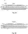
- Fig. 2A is a cross-sectional schematic of an embodiment of a device in accordance with this disclosure, shown having a gas filled enclosure (e.g., filled with N2).
- Fig. 2B is a cross-sectional schematic of an embodiment of a device in accordance with this disclosure, shown having an epoxy molded enclosure.
- Fig. 2C is a chart showing heat transfer rate vs thickness in certain embodiments.
- Fig. 3A shows an embodiment of a PCB based planar inductor for wireless signal and power transfer.
- Fig. 3A shows an embodiment of a PCB based planar inductor for wireless signal and power transfer.
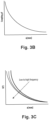
- FIG. 3B is a chart illustrating capacitor coupling vs thickness in accordance with this disclosure.
- Fig. 3C is a chart showing magnetic field vs thickness in accordance with this disclosure, showing multiple lines indicating the effect of frequency.
- Fig. 4 is a schematic circuit diagram illustrating an embodiment of a push-pull converter for wireless power and signal transfer.
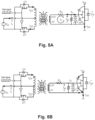
- Fig. 5A is a schematic circuit diagram of the embodiment of Fig. 4 , illustrating normal operation.
- Fig. 5B is a schematic circuit diagram of the embodiment of Fig. 5A , illustrating current flow at short circuit.
- Fig. 5C is a timing chart for the embodiment of Fig. 5A illustrating short circuit protection.
- Embodiments can provide an isolated gate driver that uses wireless power and signal transfer in a harsh environment.
- Embodiments can be used with extreme low temperature applications, especially cryogenic temperatures, or any other suitable harsh environment where components benefit from separation/isolation.
- a conventional gate driver could not be worked under cryogenics or extreme lower temperatures.
- many methods have been investigated including a special packaging design and a thermally insulated structure. However, it is not easy to meet all requirements, which includes galvanic isolation and a proper gate signal operation under cryogenics temperatures.
- this embodiments include an isolated gate driver approach for cryogenically cooled power electronics converter/inverter. However, this approach can be applied to any other harsh environment because this approach can separate the power stage and gate driver board using wireless power and signal transfer.
- Fig. 1 shows an embodiment of the disclosure which can include wireless gate signal and gate power transfer between power semiconductor board and gate driver board, incorporated signal and power signal using push-pull converter and wireless transfer, no COTS gate driver IC on the power semiconductor board and cryogenics environment, thermal isolation between gate driver board and power semiconductor board (e.g., due to insulative housing), high frequency inductive power transfer to achieve a low coupling capacitance based on PCB-based planar inductor, and short circuit protection without any other sub-circuit at the power board and cryogenics environment.
- the structure for the wireless power and signal transfer can have three areas.
- the first area can be the coldplate and semiconductor power board with cryogenics temperature (e.g., about 70K to about 120K).
- the second area can be the thermal insulation and wireless power and signal transfer with extreme low temperature (e.g., less than about 218K).
- the third area can be signal and power generation with low temperature (e.g., greater than about 273K).
- Embodiments need not include a physical wire connection between circuits. Only passive components and a planar inductor can be placed in the first area. Thus, COTS devices are not affected by the cryogenic temperatures and extreme low temperatures.
- Thermal insulation thickness and the airgap thickness for the magnetic coupling can be selected to provide desired thermal isolation and wireless transfer performance.
- two methods can include a gas nitrogen (N2) filled thermally insulated enclosure (e.g., as shown in Fig. 2A ) or a molded enclosure (e.g., as shown in Figs. 1 and 2B ). Any suitable insulation materials is contemplated herein (e.g., epoxy).
- the airgap thickness for the magnetic coupling can be designed to deliver a desired gate power and signals.
- Designing of planar coils at a high frequency operation in a compact form can be done.
- a multilayer PCB can be used, e.g., similar to the construction as shown in Fig. 3A .
- the coil has a high parasitic capacitance. This can be caused by the inter-turn capacitance due to face-to-face alignment of turns on different layers and side-by-side alignment of turns in the same layer. This lowers its self-resonance frequency.
- the coil is highly resistive, and at the resonance frequency, it changes from inductive to capacitive characteristics, which makes the design of matching network challenging.
- a single layer planar inductor can be selected for the transmission coil to reduce its parasitic capacitance (e.g., as shown in Fig. 3B ) and increase its self-resonance frequency due to transmission coil's large surface area.
- the receiving coil can have a small surface area, it can be made of a plurality (e.g., four) of layers to increase its self-inductance and the mutual inductance between two coils (e.g., as shown in Fig. 4C).
- the optimal thickness can be designs for the thermal insulation and wireless power/signal transfer.
- the push-pull converter can generate the powered gate signal that includes +/- Vgs, for example.
- a four winding method can be used.
- Fig. 4 shows a circuit diagram and the output gate-source voltage.
- the primary side can have two power switches and two winding planar inductor (transmission coils).
- the secondary side can have two winding planar inductor (receiving coils), a gate resistor and a zener diode, for example.
- short circuit protection includes the following: (1) dSAT, (2) mirror current and (3) di/dt measurement.
- Approaches can generally include a detection circuit at near power device. Thus, it is not easy to implement a short circuit protection at cryogenic temperatures due to extreme low temperature.
- embodiments can include a source current detection-based protection.
- a gate-source voltage can be fluctuated due to a high drain leakage current.
- the gate current can be a negative current that is higher than a sourcing current.
- the short-circuit can be detected by monitoring a source current in certain embodiments.
- Figs. 5A-5C shows a gate current flow and a timing chart of the short circuit protection.
- VGS gate-source voltage
- the source current (is) has a positive current always as shown in Fig. 5B.
- Fig. 5B and 5C show the current flow at the short circuit.
- the gate-source voltage (VGS) can be higher than the provided voltage that will be clamped by a Zener diode. Note that a Zener diode protects a gate-source from the over voltage.
- the gate current has over current compared to the normal sinking current.
- the source current (is) has a negative current, as shown in Fig. 5C .
- the short circuit status can be detected and dealt with.
- Embodiments can provide harsh environmental compliance through wireless gate signal and gate power transfer between power semiconductor board and gatedriver board.
- Embodiments can provide incorporated signal and power signal using single power conversion, which is push-pull converter and wireless transfer.
- Embodiments can require no COTS gate driver IC on the power semiconductor board and cryogenics environment.
- Embodiments can be thermally isolated between gate driver board and power semiconductor board.
- Embodiments can use high frequency inductive power transfer to achieve a low coupling capacitance based on PCB-based planar inductor.
- Embodiments can provide short circuit protection without any other sub-circuit at the power board and cryogenics environment.
- a conventional gate driver could not be worked under cryogenics or extreme lower temperatures.
- many methods have been investigated including a special packaging design and a thermally insulated structure.
- Embodiments presents an isolated gate driver using wireless power and signal transfer in a harsh environment.
- Embodiments can include any suitable computer hardware and/or software module(s) to perform any suitable function (e.g., as disclosed herein).
- aspects of the present disclosure may be embodied as a system, method or computer program product. Accordingly, aspects of this disclosure may take the form of an entirely hardware embodiment, an entirely software embodiment (including firmware, resident software, micro-code, etc.), or an embodiment combining software and hardware aspects, all possibilities of which can be referred to herein as a "circuit,” “module,” or “system.”
- a “circuit,” “module,” or “system” can include one or more portions of one or more separate physical hardware and/or software components that can together perform the disclosed function of the "circuit,” “module,” or “system”, or a “circuit,” “module,” or “system” can be a single self-contained unit (e.g., of hardware and/or software).
- aspects of this disclosure may take the form of a computer program product embodied in one or more computer readable medium(s) having computer readable program code embodied thereon.
- the computer readable medium may be a computer readable signal medium or a computer readable storage medium.
- a computer readable storage medium may be, for example, but not limited to, an electronic, magnetic, optical, electromagnetic, infrared, or semiconductor system, apparatus, or device, or any suitable combination of the foregoing.
- a computer readable storage medium may be any tangible medium that can contain, or store a program for use by or in connection with an instruction execution system, apparatus, or device.
- a computer readable signal medium may include a propagated data signal with computer readable program code embodied therein, for example, in baseband or as part of a carrier wave. Such a propagated signal may take any of a variety of forms, including, but not limited to, electro-magnetic, optical, or any suitable combination thereof.
- a computer readable signal medium may be any computer readable medium that is not a computer readable storage medium and that can communicate, propagate, or transport a program for use by or in connection with an instruction execution system, apparatus, or device.
- Program code embodied on a computer readable medium may be transmitted using any appropriate medium, including but not limited to wireless, wireline, optical fiber cable, RF, etc., or any suitable combination of the foregoing.
- Computer program code for carrying out operations for aspects of this disclosure may be written in any combination of one or more programming languages, including an object oriented programming language such as Java, Smalltalk, C++ or the like and conventional procedural programming languages, such as the "C" programming language or similar programming languages.
- the program code may execute entirely on the user's computer, partly on the user's computer, as a stand-alone software package, partly on the user's computer and partly on a remote computer or entirely on the remote computer or server.
- the remote computer may be connected to the user's computer through any type of network, including a local area network (LAN) or a wide area network (WAN), or the connection may be made to an external computer (for example, through the Internet using an Internet Service Provider).
- LAN local area network
- WAN wide area network
- Internet Service Provider for example, AT&T, MCI, Sprint, EarthLink, MSN, GTE, etc.
- These computer program instructions may also be stored in a computer readable medium that can direct a computer, other programmable data processing apparatus, or other devices to function in a particular manner, such that the instructions stored in the computer readable medium produce an article of manufacture including instructions which implement the function/act specified in the flowchart and/or block diagram block or blocks.
- the computer program instructions may also be loaded onto a computer, other programmable data processing apparatus, or other devices to cause a series of operational steps to be performed on the computer, other programmable apparatus or other devices to produce a computer implemented process such that the instructions which execute on the computer or other programmable apparatus provide processes for implementing the functions/acts specified herein.
- any numerical values disclosed herein can be exact values or can be values within a range. Further, any terms of approximation (e.g., “about”, “approximately”, “around”) used in this disclosure can mean the stated value within a range. For example, in certain embodiments, the range can be within (plus or minus) 20%, or within 10%, or within 5%, or within 2%, or within any other suitable percentage or number as appreciated by those having ordinary skill in the art (e.g., for known tolerance limits or error ranges).
- a reference to "A and/or B", when used in conjunction with open-ended language such as “comprising” can refer, in one embodiment, to A only (optionally including elements other than B); in another embodiment, to B only (optionally including elements other than A); in yet another embodiment, to both A and B (optionally including other elements); etc.
Landscapes
- Engineering & Computer Science (AREA)
- Power Engineering (AREA)
- Microelectronics & Electronic Packaging (AREA)
- Computer Networks & Wireless Communication (AREA)
- Physics & Mathematics (AREA)
- Thermal Sciences (AREA)
- Semiconductor Integrated Circuits (AREA)
Abstract
Description
- This disclosure relates to circuits, e.g., configured to be exposed to multiple environments.
- Certain new power electronics inverter/converter designs include cryogenic temperature portions, which can mitigate thermal limitations and power losses on the operation of aerospace power systems, for example, while significantly reducing size, weight, and power consumption. The challenges of cryogenics temperature operation for active devices, passive devices, and packaging materials is that components exhibit changes in electrical behavior as a function of temperature. These properties may further change if the materials exhibit degradation due to mechanical loading.
- Typically, some electronics devices are intended to operate at cryogenics temperatures or easily survive exposure to cryogenics temperatures. The packaging technologies between the electronics and the outside are required to survive multiple extreme low temperature cycles, which combine the challenges of cryogenics temperatures exposure and fatigue at cryogenics temperatures. Typically, a gate driver can include an isolated dc-dc power supply, gate driver integrated chip (IC), and sub-circuit that is specified to operate at low temperatures, e.g., between 125°C and -55°C. Especially, a gate driver IC and an isolated dc-dc converter are typically located in or near the power device so as to minimize a loop inductance. The power device (e.g., GaN and Si MOSFET) can be cryogenically cooled. Some near devices can be be affected by the extremely low temperature. Thus, some design difficulties to survive cryogenics temperatures include how to separate cryogenic and non-cryogenic areas, how to provide a galvanic isolated power, and how to send an isolated gate signal.
- Conventional methods and systems have generally been considered satisfactory for their intended purpose. However, there is still a need in the art for improved circuit devices. The present disclosure provides a solution for this need.
- A device can include a first circuit configured to be exposed to a first environment, the first circuit comprising one or more first transfer inductors, and a second circuit isolated from the first circuit and configured to be exposed to a second environment, the second circuit comprising one or more second transfer inductors. The second environment can be a harsh environment. The first circuit and the second circuit can be wirelessly coupled via the one or more first transfer inductors and the one or more second transfer inductors to allow transfer of power and/or signals between the first circuit and the second circuit.
- The device can be an isolated gate driver, for example. The first circuit can include one or more control electronics that are not configured to operate in the second environment. The second circuit can include power electronics including one or more power switches configured to operate in the second environment.
- The one or more first transfer inductors and the one or more second transfer inductors can include planar inductors. The one or more first transfer inductors can each be a single layer inductor. In certain embodiments, the one or more second transfer inductors can each be a multilayer planar inductor.
- The one or more power switches can be MOSFETS (e.g., GaN). Any other suitable power switch type is contemplated herein. The one or more control electronics can be configured to provide gate signals to the one or more power switches via the first and second transfer inductors to control a state of the one or more power switches.
- In certain embodiments, each first transfer inductor can include two first windings having a first turn amount and a second turn amount, respectively. In certain embodiments, each second transfer inductor can include two second windings having a third turn amount and a fourth turn amount respectively. In certain embodiments, the first turn amount can be greater than the second turn amount, which can be greater than the third turn amount, which can be greater than the fourth turn amount. In certain embodiments, the first turn amount is 65 turns, the second turn amount is 21 turns, the third turn amount is 20 turns, and the fourth turn amount is 1 turn. Any suitable number of turns for each inductor is contemplated herein (e.g., to provide a desired power/signal transfer).
- The distance between the one or more first transfer inductors and one or more second transfer inductors can be set to provide a desired power transfer. For example, in certain embodiments, the desired power transfer can be 2 to 3 watts of power at about 100kHz frequency.
- In certain embodiments, the second environment can be a cryogenic environment. For example, the second environment can have a temperature between about 70K and about 120K. The first environment can have a temperature greater than about 273K, for example.
- In certain embodiments, the device can further include a cold plate connected to the second circuit and configured to allow cryogenic flow through a channel in the cold plate. The second circuit and the cold plate can be contained within a housing. The first circuit can be mounted to an outside of the housing to be thermally isolated from the second environment, for example.
- In certain embodiments, the one or more control electronics can include a first switch and a second switch configured to control signal flow to the first transfer inductors. The one or more power electronics can further include one or more zener diodes and a gate resistor, for example. Certain embodiments can include a control module configured to provide gate signals to the first switch and the second switch to control a state of the first and second switch. The control module can be configured to sense when a source current becomes opposite, and can be configured to open the first switch and the second switch to short circuit power to the first transfer inductors to avoid transferring power from the first circuit to the second circuit.
- These and other features of the embodiments of the subject disclosure will become more readily apparent to those skilled in the art from the following detailed description taken in conjunction with the drawings.
- So that those skilled in the art to which the subject disclosure appertains will readily understand how to make and use the devices and methods of the subject disclosure without undue experimentation, embodiments thereof will be described in detail herein below with reference to certain figures, wherein:
-
Fig. 1 is a schematic diagram showing a cross-sectional view showing an embodiment of a device in accordance with this disclosure, as well as schematically showing a first circuit and a second circuit having wireless power and signal transfer in accordance with this disclosure; -
Fig. 2A is a cross-sectional schematic of an embodiment of a device in accordance with this disclosure, shown having a gas filled enclosure (e.g., filled with N2); -
Fig. 2B is a cross-sectional schematic of an embodiment of a device in accordance with this disclosure, shown having an epoxy molded enclosure; -
Fig. 2C is a chart showing heat transfer rate vs thickness in certain embodiments; -
Fig. 3A shows an embodiment of a PCB based planar inductor for wireless signal and power transfer; -
Fig. 3B is a chart illustrating capacitor coupling vs thickness in accordance with this disclosure; -
Fig. 3C is a chart showing magnetic field vs thickness in accordance with this disclosure, showing multiple lines indicating the effect of frequency; -
Fig. 4 is a schematic circuit diagram illustrating an embodiment of a push-pull converter for wireless power and signal transfer; -
Fig. 5A is a schematic circuit diagram of the embodiment ofFig. 4 , illustrating normal operation; -
Fig. 5B is a schematic circuit diagram of the embodiment ofFig. 5A , illustrating current flow at short circuit; and -
Fig. 5C is a timing chart for the embodiment ofFig. 5A illustrating short circuit protection. - Reference will now be made to the drawings wherein like reference numerals identify similar structural features or aspects of the subject disclosure. For purposes of explanation and illustration, and not limitation, an illustrative view of an embodiment of a device in accordance with the disclosure is shown in
Fig. 1 and is designated generally byreference character 100. Other embodiments and/or aspects of this disclosure are shown inFigs. 2A-5C . - Referring to Fig. 1A, a
device 100 can include afirst circuit 101 configured to be exposed to a first environment (e.g., ambient air). Thefirst circuit 101 can include one or morefirst transfer inductors 101a. - The
device 100 can includesecond circuit 103 isolated (e.g., thermally) from thefirst circuit 101. Thesecond circuit 103 can be configured to be exposed to a second environment (i.e., different than the first environment) and can include one or moresecond transfer inductors 103a. The second environment can be a harsh environment (e.g., thermally extreme such as a cryogenic environment, and/or any other type of environment that the functionality of one or more components of thefirst circuit 101 would have reduced functionality). - The
first circuit 101 and thesecond circuit 103 can be wirelessly coupled via the one or morefirst transfer inductors 101a and the one or moresecond transfer inductors 103a to allow transfer of power and/or signals between thefirst circuit 101 and the second circuit 103 (e.g., transmission from thefirst circuit 101 to the second circuit 103). - In certain embodiments, the
device 100 can be an isolated gate driver (e.g., for power systems for aircraft), for example. Thefirst circuit 101 can include one ormore control electronics 105 that are not configured to operate in the second environment, for example. Thefirst circuit 101 have a PCB made of FR4, in certain embodiments. Any other suitable material is contemplated herein. In certain embodiments, the one ormore control electronics 105 can include afirst switch 105a and asecond switch 105b configured to control signal flow to thefirst transfer inductors 101a. - The
control electronics 105 can include avoltage source 105c. As shown inFig. 1 , thedevice 100 can include a plurality of the control electronics 105 (e.g., connected to thevoltage source 105 c) and a plurality ofrespective inductors 101a. As shown, eachfirst transfer inductor 105a can be connected between each pair ofswitches switches first transfer inductor 105a. Thevoltage source 105c can have one terminal connected to the pair ofswitches first transfer inductor 105a. - Certain embodiments can include a
control module 106 configured to provide gate signals (e.g., a PWM signal as shown) to thefirst switch 105a and thesecond switch 105b to control a state of the first andsecond switch 105a, b. In certain embodiments, thecontrol module 106 can include protection logic. For example, thecontrol module 106 can be configured to sense when a source current becomes opposite (e.g., when the current goes negative), and can be configured to open thefirst switch 105a and thesecond switch 105b to short circuit power to the first transfer inductors to avoid transferring power from the first circuit to the second circuit. Any suitable protection scheme, e.g., as described below, is contemplated herein. The control module can include any suitable hardware and/or software module(s) configured to perform any suitable function disclosed herein and/or otherwise. - The
second circuit 103 can includepower electronics 107 including one or more power switches 109 (e.g., GaN MOSFETs) configured to operate in the second environment. The one ormore power electronics 107 can further include one or more zener diodes 111a and a gate resistor 11 1b, for example. Any other suitable components for thesecond circuit 103 that can operate as desired in a harsh environment are contemplated herein. - The one or
more power switches 109 can be MOSFETS (e.g., GaN). Any other suitable power switch type is contemplated herein. The one ormore control electronics 105 can be configured to provide gate signals to the one ormore power switches 109 via the first andsecond transfer inductors power switch 109 can be connected to a respectivesecond transfer inductor 103a to receive signals therefrom. The power switches 109 can be on a power line (e.g., source and drain connected to a high voltage line to selective allow current on the line). - Referring additionally to
Figs. 2A, 2B , and2C , thedevice 100 can have a suitable housing. For example, as shown inFig. 2A , thedevice 100 can include ahollow housing 213a configured to be filled with a gas (e.g., N2), containing thesecond circuit 103. In certain embodiments, as shown inFig. 2B , thedevice 100 can include asolid housing 213b (e.g., an epoxy molded enclosure) containing thesecond circuit 103. Any other suitable housing that isolates thefirst circuit 101 and thesecond circuit 103 is contemplated herein. - In certain embodiments, referring additionally to
Figs. 3A ,3B, and 3C , the one or morefirst transfer inductors 101a and the one or moresecond transfer inductors 103a can include planar inductors as shown. The one or morefirst transfer inductors 101a can each be a single layer inductor, for example. In certain embodiments, the one or moresecond transfer inductors 103a can each be a multilayer planar inductor (e.g., a smaller area than a respectivefirst transfer inductor 101a, but vertically stacked). - In certain embodiments, each
first transfer inductor 101a can include twofirst windings second transfer inductor 103a can include twosecond windings - The distance (shown as D or x) between the one or more
first transfer inductors 101a and one or moresecond transfer inductors 103a can be set to provide a desired power transfer. For example, in certain embodiments, the desired power transfer can be 2 to 3 watts of power, e.g., at about 100kHz frequency of input signal. Any suitable distance for any suitable power transfer is contemplated herein.Figs. 3B and 3C illustrate the effect of distance on coupling and magnetic field. - In certain embodiments, the second environment can be a cryogenic environment. For example, the second environment can have a temperature between about 70K and about 120K. The first environment can have a temperature greater than about 273K, for example.
- In certain embodiments, the
device 100 can further include a cold plate 117 connected to thesecond circuit 103 and configured to allow cryogenic flow (e.g., N2 or Ar2 or any other suitable cryogenic flow) through achannel 117a in the cold plate 117. Thesecond circuit 103 and the cold plate 117 can be contained within ahousing first circuit 101 can be mounted to an outside of thehousing - In embodiments, GaN or Si MOSFETS can be used for very high power AC/DC converter systems. GaN and Si, for example, become lower resistance with cryogenic cooling. Wireless signal and power transfer allows elimination of certain physical components and integrated circuits within the cryogenic environment that cannot withstand such a harsh environment. Copper line inductors are not affected by cryogenic temperatures, for example.
- Embodiments can include only cold temperature robust components, e.g., silicone diodes, resistors, and transfer inductors, and no integrated circuitry. One having ordinary skill in the art in view of this disclosure understands how to select a desired distance between inductors to provide a desired power transfer at a certain frequency, and without undue experimentation, while also allowing for thermal isolation of the first circuit and the second circuit.
-
Fig. 1 is a schematic diagram showing a cross-sectional view showing an embodiment of a device in accordance with this disclosure, as well as schematically showing a first circuit and a second circuit having wireless power and signal transfer in accordance with this disclosure.Fig. 2A is a cross-sectional schematic of an embodiment of a device in accordance with this disclosure, shown having a gas filled enclosure (e.g., filled with N2).Fig. 2B is a cross-sectional schematic of an embodiment of a device in accordance with this disclosure, shown having an epoxy molded enclosure.Fig. 2C is a chart showing heat transfer rate vs thickness in certain embodiments.Fig. 3A shows an embodiment of a PCB based planar inductor for wireless signal and power transfer.Fig. 3B is a chart illustrating capacitor coupling vs thickness in accordance with this disclosure.Fig. 3C is a chart showing magnetic field vs thickness in accordance with this disclosure, showing multiple lines indicating the effect of frequency.Fig. 4 is a schematic circuit diagram illustrating an embodiment of a push-pull converter for wireless power and signal transfer.Fig. 5A is a schematic circuit diagram of the embodiment ofFig. 4 , illustrating normal operation.Fig. 5B is a schematic circuit diagram of the embodiment ofFig. 5A , illustrating current flow at short circuit.Fig. 5C is a timing chart for the embodiment ofFig. 5A illustrating short circuit protection. - Embodiments can provide an isolated gate driver that uses wireless power and signal transfer in a harsh environment. Embodiments can be used with extreme low temperature applications, especially cryogenic temperatures, or any other suitable harsh environment where components benefit from separation/isolation. Typically, a conventional gate driver could not be worked under cryogenics or extreme lower temperatures. In order to overcome the environment, many methods have been investigated including a special packaging design and a thermally insulated structure. However, it is not easy to meet all requirements, which includes galvanic isolation and a proper gate signal operation under cryogenics temperatures. Thus, this embodiments include an isolated gate driver approach for cryogenically cooled power electronics converter/inverter. However, this approach can be applied to any other harsh environment because this approach can separate the power stage and gate driver board using wireless power and signal transfer.
- In order to resolve traditional issues, many methods have been investigated such as a low temperature device packaging and a thermally insulated packaging. The special packaging design that the target is an electronics device and passive components, especially an isolation transformer. In this case, it is necessary to have a special design based on a thermally insulated packaging and a special material. While this method can provide the high reliable operation at the harsh and extreme low temperature, it is a very expensive solution and is not easy to design the individual packaging for each application. Other approaches can include using a thermally insulated structure that has features such as very simple structure and signal/power wiring. An isolated DC-DC converter and gate driver can be located at the outside enclosure, which can be a room temperature area. Thus, off-the shelf parts can be used. However, this method depends on the hard wiring both signal and power. The switching frequency can be limited due to cable length and loop inductance. In order to minimize this impact, a push-pull circuit can be added. However, the push-pull circuit will be exposed at the extreme low temperature if applied traditionally.
-
Fig. 1 shows an embodiment of the disclosure which can include wireless gate signal and gate power transfer between power semiconductor board and gate driver board, incorporated signal and power signal using push-pull converter and wireless transfer, no COTS gate driver IC on the power semiconductor board and cryogenics environment, thermal isolation between gate driver board and power semiconductor board (e.g., due to insulative housing), high frequency inductive power transfer to achieve a low coupling capacitance based on PCB-based planar inductor, and short circuit protection without any other sub-circuit at the power board and cryogenics environment. - The structure for the wireless power and signal transfer can have three areas. The first area can be the coldplate and semiconductor power board with cryogenics temperature (e.g., about 70K to about 120K). The second area can be the thermal insulation and wireless power and signal transfer with extreme low temperature (e.g., less than about 218K). The third area can be signal and power generation with low temperature (e.g., greater than about 273K).
- Embodiments need not include a physical wire connection between circuits. Only passive components and a planar inductor can be placed in the first area. Thus, COTS devices are not affected by the cryogenic temperatures and extreme low temperatures. Thermal insulation thickness and the airgap thickness for the magnetic coupling can be selected to provide desired thermal isolation and wireless transfer performance. For the thermal insulation, two methods can include a gas nitrogen (N2) filled thermally insulated enclosure (e.g., as shown in
Fig. 2A ) or a molded enclosure (e.g., as shown inFigs. 1 and2B ). Any suitable insulation materials is contemplated herein (e.g., epoxy). - The airgap thickness for the magnetic coupling can be designed to deliver a desired gate power and signals. Designing of planar coils at a high frequency operation in a compact form can be done. To miniaturize a coil, a multilayer PCB can be used, e.g., similar to the construction as shown in
Fig. 3A . In that case, the coil has a high parasitic capacitance. This can be caused by the inter-turn capacitance due to face-to-face alignment of turns on different layers and side-by-side alignment of turns in the same layer. This lowers its self-resonance frequency. Around the self-resonance frequency, the coil is highly resistive, and at the resonance frequency, it changes from inductive to capacitive characteristics, which makes the design of matching network challenging. Accordingly, in certain embodiments, a single layer planar inductor can be selected for the transmission coil to reduce its parasitic capacitance (e.g., as shown inFig. 3B ) and increase its self-resonance frequency due to transmission coil's large surface area. Since the receiving coil can have a small surface area, it can be made of a plurality (e.g., four) of layers to increase its self-inductance and the mutual inductance between two coils (e.g., as shown in Fig. 4C). To that end, the optimal thickness can be designs for the thermal insulation and wireless power/signal transfer. - The push-pull converter can generate the powered gate signal that includes +/- Vgs, for example. In order to generate negative voltage at the gate-source, a four winding method can be used.
Fig. 4 shows a circuit diagram and the output gate-source voltage. The primary side can have two power switches and two winding planar inductor (transmission coils). The secondary side can have two winding planar inductor (receiving coils), a gate resistor and a zener diode, for example. - Typically, short circuit protection includes the following: (1) dSAT, (2) mirror current and (3) di/dt measurement. Approaches can generally include a detection circuit at near power device. Thus, it is not easy to implement a short circuit protection at cryogenic temperatures due to extreme low temperature. In order to avoid the low temperature, embodiments can include a source current detection-based protection. At the short-circuit event, a gate-source voltage can be fluctuated due to a high drain leakage current. Thus, the gate current can be a negative current that is higher than a sourcing current. Thus, the short-circuit can be detected by monitoring a source current in certain embodiments.
-
Figs. 5A-5C shows a gate current flow and a timing chart of the short circuit protection. At the normal operation, embodiments can provide +15/-5V gate-source voltage (VGS) that Cgs has a charging/discharging repeatably, as shown inFig. 5A . The source current (is) has a positive current always as shown inFig. 5B. Fig. 5B and5C show the current flow at the short circuit. At very high drain current, the gate-source voltage (VGS) can be higher than the provided voltage that will be clamped by a Zener diode. Note that a Zener diode protects a gate-source from the over voltage. The gate current has over current compared to the normal sinking current. Thus, the source current (is) has a negative current, as shown inFig. 5C . The short circuit status can be detected and dealt with. - Embodiments can provide harsh environmental compliance through wireless gate signal and gate power transfer between power semiconductor board and gatedriver board. Embodiments can provide incorporated signal and power signal using single power conversion, which is push-pull converter and wireless transfer. Embodiments can require no COTS gate driver IC on the power semiconductor board and cryogenics environment. Embodiments can be thermally isolated between gate driver board and power semiconductor board. Embodiments can use high frequency inductive power transfer to achieve a low coupling capacitance based on PCB-based planar inductor. Embodiments can provide short circuit protection without any other sub-circuit at the power board and cryogenics environment.
- Typically, a conventional gate driver could not be worked under cryogenics or extreme lower temperatures. In order to overcome the environment, many methods have been investigated including a special packaging design and a thermally insulated structure. However, it is not easy to meet all requirements, which include a galvanic isolation and a proper gate signal operation under cryogenics temperatures. Embodiments presents an isolated gate driver using wireless power and signal transfer in a harsh environment.
- Embodiments can include any suitable computer hardware and/or software module(s) to perform any suitable function (e.g., as disclosed herein).
- As will be appreciated by those skilled in the art, aspects of the present disclosure may be embodied as a system, method or computer program product. Accordingly, aspects of this disclosure may take the form of an entirely hardware embodiment, an entirely software embodiment (including firmware, resident software, micro-code, etc.), or an embodiment combining software and hardware aspects, all possibilities of which can be referred to herein as a "circuit," "module," or "system." A "circuit," "module," or "system" can include one or more portions of one or more separate physical hardware and/or software components that can together perform the disclosed function of the "circuit," "module," or "system", or a "circuit," "module," or "system" can be a single self-contained unit (e.g., of hardware and/or software). Furthermore, aspects of this disclosure may take the form of a computer program product embodied in one or more computer readable medium(s) having computer readable program code embodied thereon.
- Any combination of one or more computer readable medium(s) may be utilized. The computer readable medium may be a computer readable signal medium or a computer readable storage medium. A computer readable storage medium may be, for example, but not limited to, an electronic, magnetic, optical, electromagnetic, infrared, or semiconductor system, apparatus, or device, or any suitable combination of the foregoing. More specific examples (a non-exhaustive list) of the computer readable storage medium would include the following: an electrical connection having one or more wires, a portable computer diskette, a hard disk, a random access memory (RAM), a read-only memory (ROM), an erasable programmable read-only memory (EPROM or Flash memory), an optical fiber, a portable compact disc read-only memory (CD-ROM), an optical storage device, a magnetic storage device, or any suitable combination of the foregoing. In the context of this document, a computer readable storage medium may be any tangible medium that can contain, or store a program for use by or in connection with an instruction execution system, apparatus, or device.
- A computer readable signal medium may include a propagated data signal with computer readable program code embodied therein, for example, in baseband or as part of a carrier wave. Such a propagated signal may take any of a variety of forms, including, but not limited to, electro-magnetic, optical, or any suitable combination thereof. A computer readable signal medium may be any computer readable medium that is not a computer readable storage medium and that can communicate, propagate, or transport a program for use by or in connection with an instruction execution system, apparatus, or device.
- Program code embodied on a computer readable medium may be transmitted using any appropriate medium, including but not limited to wireless, wireline, optical fiber cable, RF, etc., or any suitable combination of the foregoing.
- Computer program code for carrying out operations for aspects of this disclosure may be written in any combination of one or more programming languages, including an object oriented programming language such as Java, Smalltalk, C++ or the like and conventional procedural programming languages, such as the "C" programming language or similar programming languages. The program code may execute entirely on the user's computer, partly on the user's computer, as a stand-alone software package, partly on the user's computer and partly on a remote computer or entirely on the remote computer or server. In the latter scenario, the remote computer may be connected to the user's computer through any type of network, including a local area network (LAN) or a wide area network (WAN), or the connection may be made to an external computer (for example, through the Internet using an Internet Service Provider).
- Aspects of this disclosure may be described above with reference to flowchart illustrations and/or block diagrams of methods, apparatus (systems) and computer program products according to embodiments of this disclosure. It will be understood that each block of any flowchart illustrations and/or block diagrams, and combinations of blocks in any flowchart illustrations and/or block diagrams, can be implemented by computer program instructions. These computer program instructions may be provided to a processor of a general purpose computer, special purpose computer, or other programmable data processing apparatus to produce a machine, such that the instructions, which execute via the processor of the computer or other programmable data processing apparatus, create means for implementing the functions/acts specified in any flowchart and/or block diagram block or blocks.
- These computer program instructions may also be stored in a computer readable medium that can direct a computer, other programmable data processing apparatus, or other devices to function in a particular manner, such that the instructions stored in the computer readable medium produce an article of manufacture including instructions which implement the function/act specified in the flowchart and/or block diagram block or blocks.
- The computer program instructions may also be loaded onto a computer, other programmable data processing apparatus, or other devices to cause a series of operational steps to be performed on the computer, other programmable apparatus or other devices to produce a computer implemented process such that the instructions which execute on the computer or other programmable apparatus provide processes for implementing the functions/acts specified herein.
- Those having ordinary skill in the art understand that any numerical values disclosed herein can be exact values or can be values within a range. Further, any terms of approximation (e.g., "about", "approximately", "around") used in this disclosure can mean the stated value within a range. For example, in certain embodiments, the range can be within (plus or minus) 20%, or within 10%, or within 5%, or within 2%, or within any other suitable percentage or number as appreciated by those having ordinary skill in the art (e.g., for known tolerance limits or error ranges).
- The articles "a", "an", and "the" as used herein and in the appended claims are used herein to refer to one or to more than one (i.e., to at least one) of the grammatical object of the article unless the context clearly indicates otherwise. By way of example, "an element" means one element or more than one element.
- The phrase "and/or," as used herein in the specification and in the claims, should be understood to mean "either or both" of the elements so conjoined, i.e., elements that are conjunctively present in some cases and disjunctively present in other cases. Multiple elements listed with "and/or" should be construed in the same fashion, i.e., "one or more" of the elements so conjoined. Other elements may optionally be present other than the elements specifically identified by the "and/or" clause, whether related or unrelated to those elements specifically identified. Thus, as a non-limiting example, a reference to "A and/or B", when used in conjunction with open-ended language such as "comprising" can refer, in one embodiment, to A only (optionally including elements other than B); in another embodiment, to B only (optionally including elements other than A); in yet another embodiment, to both A and B (optionally including other elements); etc.
- As used herein in the specification and in the claims, "or" should be understood to have the same meaning as "and/or" as defined above. For example, when separating items in a list, "or" or "and/or" shall be interpreted as being inclusive, i.e., the inclusion of at least one, but also including more than one, of a number or list of elements, and, optionally, additional unlisted items. Only terms clearly indicated to the contrary, such as "only one of" or "exactly one of," or, when used in the claims, "consisting of," will refer to the inclusion of exactly one element of a number or list of elements. In general, the term "or" as used herein shall only be interpreted as indicating exclusive alternatives (i.e., "one or the other but not both") when preceded by terms of exclusivity, such as "either," "one of," "only one of," or "exactly one of."
- Any suitable combination(s) of any disclosed embodiments and/or any suitable portion(s) thereof are contemplated herein as appreciated by those having ordinary skill in the art in view of this disclosure.
- The embodiments of the present disclosure, as described above and shown in the drawings, provide for improvement in the art to which they pertain. While the subject disclosure includes reference to certain embodiments, those skilled in the art will readily appreciate that changes and/or modifications may be made thereto without departing from the spirit and scope of the subject disclosure.
Claims (15)
- A device, comprising:a first circuit (101) to be exposed to a first environment, the first circuit (101) comprising one or more first transfer inductors (101a);a second circuit (103) isolated from the first circuit (101) and configured to be exposed to a second environment, the second circuit (103) comprising one or more second transfer inductors (103a), wherein the second environment is a harsh environment, and wherein the first circuit (101) and the second circuit (103) are wirelessly coupled via the one or more first transfer inductors (101a) and the one or more second transfer inductors (103a) to allow transfer of power and/or signals between the first circuit (101) and the second circuit.
- The device of claim 1, wherein the device is an isolated gate driver.
- The device of claim 1 or 2, wherein the first circuit (101) includes one or more control electronics that are not configured to operate in the second environment, and the second circuit (103) includes power electronics including one or more switches configured to operate in the second environment.
- The device of any preceding claim, wherein the one or more first transfer inductors (101a) and the one or more second transfer inductors (103a) include planar inductors.
- The device of any preceding claim, wherein the one or more first transfer inductors (101a) are each a single layer inductor.
- The device of any preceding claim, wherein the one or more second transfer inductors (103a) are each a multilayer planar inductor.
- The device of any preceding claim, wherein the one or more switches are MOSFETS.
- The device of any preceding claim, wherein the one or more control electronics are configured to provide gate signals to the one or more switches via the first and second transfer inductors (103a) to control a state of the one or more switches.
- The device of any preceding claim, wherein each first transfer inductor includes two first windings having a first turn amount and a second turn amount, respectively, and wherein each second transfer inductor includes two second windings having a third turn amount and a fourth turn amount respectively.
- The device of claim 9, wherein the first turn amount is greater than the second turn amount, which is greater than the third turn amount, which is greater than the fourth turn amount, and optionally wherein the first turn amount is 65 turns, the second turn amount is 21 turns, the third turn amount is 20 turns, and the fourth turn amount is 1 turn.
- The device of claim 9, wherein the distance between the one or more first transfer inductors (101a) and one or more second transfer inductors (103a) is set to provide a desired power transfer.
- The device of claim 11, wherein the desired power transfer is 2 to 3 watts of power at about 100kHz frequency.
- The device of claim 12, wherein the second environment is a cryogenic environment, or wherein the second environment has a temperature between about 70K and about 120K, or wherein the first environment has a temperature greater than about 273K.
- The device of claim 13, further comprising a cold plate connected to the second circuit (103) and configured to allow cryogenic flow through a channel in the cold plate, and optionally wherein the second circuit (103) and the cold plate are contained within a housing, wherein the first circuit (101) is mounted to an outside of the housing to be thermally isolated from the second environment.
- The device of claim 14, wherein the one or more control electronics include a first switch and a second switch configured to control signal flow to the first transfer inductors (101a) , wherein the one or more power electronics include one or more zener diodes and a gate resistor, and optionally further comprising a control module configured to provide gate signals to the first switch and the second switch to control a state of the first and second switch, wherein the control module is configured to sense when a source current becomes opposite, and is configured to open the first switch and the second switch to short circuit power to the first transfer inductors (101a) to avoid transferring power from the first circuit (101) to the second circuit.
Applications Claiming Priority (1)
| Application Number | Priority Date | Filing Date | Title |
|---|---|---|---|
| US17/739,809 US11670967B1 (en) | 2022-05-09 | 2022-05-09 | Multi-environmental circuit devices |
Publications (1)
| Publication Number | Publication Date |
|---|---|
| EP4277101A1 true EP4277101A1 (en) | 2023-11-15 |
Family
ID=86330558
Family Applications (1)
| Application Number | Title | Priority Date | Filing Date |
|---|---|---|---|
| EP23172055.8A Pending EP4277101A1 (en) | 2022-05-09 | 2023-05-08 | Multi-environmental circuit devices |
Country Status (2)
| Country | Link |
|---|---|
| US (1) | US11670967B1 (en) |
| EP (1) | EP4277101A1 (en) |
Families Citing this family (1)
| Publication number | Priority date | Publication date | Assignee | Title |
|---|---|---|---|---|
| FR3155666A1 (en) * | 2023-11-22 | 2025-05-23 | Vitesco Technologies | SYSTEM FOR CONVERTING A FIRST ELECTRICAL VOLTAGE INTO A SECOND ELECTRICAL VOLTAGE COMPRISING AT LEAST ONE PASSIVE VOLTAGE LIMITER COMPONENT |
Citations (6)
| Publication number | Priority date | Publication date | Assignee | Title |
|---|---|---|---|---|
| EP2157689A1 (en) * | 2007-11-20 | 2010-02-24 | Aisin AW Co., Ltd. | Motor control device |
| EP2763299A1 (en) * | 2011-09-28 | 2014-08-06 | Sanken Electric Co., Ltd. | Gate drive circuit |
| US20170070354A1 (en) * | 2015-09-09 | 2017-03-09 | Stmicroelectronics S.R.L. | A method of transmitting power and data across a galvanic isolation barrier, corresponding system and apparatus |
| US20180212506A1 (en) * | 2015-08-03 | 2018-07-26 | Iie Gmbh & Co. Kg | Asymmetrical bipolar voltage supply |
| EP3407366A1 (en) * | 2017-05-24 | 2018-11-28 | General Electric Company | Integrated system for signal and power transmission with galvanic isolation |
| CN112514222A (en) * | 2020-01-21 | 2021-03-16 | 深圳市大疆创新科技有限公司 | Demodulation circuit, pulse generation circuit and isolation drive circuit for isolation drive circuit |
Family Cites Families (11)
| Publication number | Priority date | Publication date | Assignee | Title |
|---|---|---|---|---|
| US7711322B2 (en) * | 2005-06-15 | 2010-05-04 | Wireless Fibre Systems | Underwater communications system and method |
| US7777370B2 (en) | 2007-05-03 | 2010-08-17 | Honeywell International Inc. | Integrated gate drive for use in control and protection of power modules |
| US7800222B2 (en) | 2007-11-29 | 2010-09-21 | Infineon Technologies Ag | Semiconductor module with switching components and driver electronics |
| US7956566B2 (en) | 2008-01-22 | 2011-06-07 | International Rectifier Corporation | Driver IC with HV-isolation, especially hybrid electric vehicle motor drive concept |
| US20100250058A1 (en) * | 2009-03-31 | 2010-09-30 | Joseph Bernard Steffler | Systems and method for protected memory |
| US8946941B2 (en) * | 2010-09-14 | 2015-02-03 | Monterey Bay Aquarium Research Institute | Wireless power and data transfer device for harsh and extreme environments |
| US9002265B2 (en) | 2012-07-26 | 2015-04-07 | General Electric Company | Method, system and apparatus for galvanic isolation of gate-controlled devices |
| US10317484B2 (en) | 2014-10-09 | 2019-06-11 | General Electric Company | Method and system for contactless power transfer in a gate driver unit |
| US9685947B2 (en) | 2015-03-30 | 2017-06-20 | Halliburton Energy Services, Inc. | Simplified gate driver for power transistors |
| EP3514928B1 (en) | 2018-01-19 | 2021-03-03 | Hamilton Sundstrand Corporation | Gate driver |
| US11435770B2 (en) | 2020-01-08 | 2022-09-06 | Texas Instruments Incorporated | Fixed current-gain booster for capacitive gate power device with input voltage control |
-
2022
- 2022-05-09 US US17/739,809 patent/US11670967B1/en active Active
-
2023
- 2023-05-08 EP EP23172055.8A patent/EP4277101A1/en active Pending
Patent Citations (6)
| Publication number | Priority date | Publication date | Assignee | Title |
|---|---|---|---|---|
| EP2157689A1 (en) * | 2007-11-20 | 2010-02-24 | Aisin AW Co., Ltd. | Motor control device |
| EP2763299A1 (en) * | 2011-09-28 | 2014-08-06 | Sanken Electric Co., Ltd. | Gate drive circuit |
| US20180212506A1 (en) * | 2015-08-03 | 2018-07-26 | Iie Gmbh & Co. Kg | Asymmetrical bipolar voltage supply |
| US20170070354A1 (en) * | 2015-09-09 | 2017-03-09 | Stmicroelectronics S.R.L. | A method of transmitting power and data across a galvanic isolation barrier, corresponding system and apparatus |
| EP3407366A1 (en) * | 2017-05-24 | 2018-11-28 | General Electric Company | Integrated system for signal and power transmission with galvanic isolation |
| CN112514222A (en) * | 2020-01-21 | 2021-03-16 | 深圳市大疆创新科技有限公司 | Demodulation circuit, pulse generation circuit and isolation drive circuit for isolation drive circuit |
Non-Patent Citations (1)
| Title |
|---|
| BARTH CHRISTOPHER ET AL: "Experimental evaluation of a 1 kW, single-phase, 3-level gallium nitride inverter in extreme cold environment", 2017 IEEE APPLIED POWER ELECTRONICS CONFERENCE AND EXPOSITION (APEC), IEEE, 26 March 2017 (2017-03-26), pages 717 - 723, XP033098313, DOI: 10.1109/APEC.2017.7930773 * |
Also Published As
| Publication number | Publication date |
|---|---|
| US11670967B1 (en) | 2023-06-06 |
Similar Documents
| Publication | Publication Date | Title |
|---|---|---|
| CN104578439B (en) | Device for wireless charging link | |
| US11676884B2 (en) | Cantilevered leadframe support structure for magnetic wireless transfer between integrated circuit dies | |
| US10256718B2 (en) | Low-inductance half-bridge arrangement | |
| US10832858B2 (en) | High-frequency transformer design for DC/DC resonant converters | |
| CN103023278B (en) | Compact isolated switching power converter | |
| CN107852093B (en) | Power conversion device | |
| AU2009258828B2 (en) | Refrigeration apparatus | |
| US20200258675A1 (en) | Hybrid transformer for dc/dc converter | |
| RU2702103C2 (en) | Inverter with high specific power | |
| CN106130322B (en) | Gate driving circuit for reducing parasitic coupling | |
| EP4277101A1 (en) | Multi-environmental circuit devices | |
| Dong et al. | Design of high-speed H-bridge converter using discrete SiC MOSFETs for solid-state transformer applications | |
| KR100742104B1 (en) | Multifunction lead frame and integrated circuit package incorporating the same | |
| Tang et al. | A low-profile low-power converter with coreless PCB isolation transformer | |
| Halsted et al. | A critique of little box challenge inverter designs: Breaking from traditional design tradeoffs | |
| Park et al. | A bare-die SiC-based isolated bidirectional DC-DC converter for electric vehicle on-board chargers | |
| Rajagopal et al. | Design, fabrication, and testing of a 1.7 kV SiC switching cell for a high-density integrated power electronics building block (iPEBB) | |
| Liu et al. | Pcb layout evaluation of gan hemt power loop | |
| Cooper | Power module integration: A new approach | |
| Rajagopal | Design of 1.7 kV SiC MOSFET Switching-Cells for Integrated Power Electronics Building Block (iPEBB) | |
| Papadopoulos et al. | Formula evaluation and voltage distribution of planar transformers using rectangular windings | |
| Wang | High power density and high temperature converter design for transportation applications | |
| Yu et al. | An integrated GaN-based converter based on cooling-system-inductor structure for point-of-load converters | |
| Gurusamy | Design and analysis of integrated planar transformer for llc converter | |
| McClusky | High voltage resonant self-tracking current-fed converter |
Legal Events
| Date | Code | Title | Description |
|---|---|---|---|
| PUAI | Public reference made under article 153(3) epc to a published international application that has entered the european phase |
Free format text: ORIGINAL CODE: 0009012 |
|
| STAA | Information on the status of an ep patent application or granted ep patent |
Free format text: STATUS: THE APPLICATION HAS BEEN PUBLISHED |
|
| AK | Designated contracting states |
Kind code of ref document: A1 Designated state(s): AL AT BE BG CH CY CZ DE DK EE ES FI FR GB GR HR HU IE IS IT LI LT LU LV MC ME MK MT NL NO PL PT RO RS SE SI SK SM TR |
|
| STAA | Information on the status of an ep patent application or granted ep patent |
Free format text: STATUS: REQUEST FOR EXAMINATION WAS MADE |
|
| 17P | Request for examination filed |
Effective date: 20240514 |
|
| RBV | Designated contracting states (corrected) |
Designated state(s): AL AT BE BG CH CY CZ DE DK EE ES FI FR GB GR HR HU IE IS IT LI LT LU LV MC ME MK MT NL NO PL PT RO RS SE SI SK SM TR |
|
| STAA | Information on the status of an ep patent application or granted ep patent |
Free format text: STATUS: EXAMINATION IS IN PROGRESS |
|
| 17Q | First examination report despatched |
Effective date: 20250723 |