RU2702103C2 - Inverter with high specific power - Google Patents
Inverter with high specific power Download PDFInfo
- Publication number
- RU2702103C2 RU2702103C2 RU2018104099A RU2018104099A RU2702103C2 RU 2702103 C2 RU2702103 C2 RU 2702103C2 RU 2018104099 A RU2018104099 A RU 2018104099A RU 2018104099 A RU2018104099 A RU 2018104099A RU 2702103 C2 RU2702103 C2 RU 2702103C2
- Authority
- RU
- Russia
- Prior art keywords
- power inverter
- capacitors
- heat sink
- layer
- output
- Prior art date
Links
- 239000003990 capacitor Substances 0.000 claims abstract description 34
- 238000001914 filtration Methods 0.000 claims abstract description 16
- 239000004065 semiconductor Substances 0.000 claims abstract description 14
- 239000000919 ceramic Substances 0.000 claims description 9
- RYGMFSIKBFXOCR-UHFFFAOYSA-N Copper Chemical compound [Cu] RYGMFSIKBFXOCR-UHFFFAOYSA-N 0.000 claims description 8
- 239000003985 ceramic capacitor Substances 0.000 claims description 8
- 229910052802 copper Inorganic materials 0.000 claims description 8
- 239000010949 copper Substances 0.000 claims description 8
- 229910000859 α-Fe Inorganic materials 0.000 claims description 7
- 238000009826 distribution Methods 0.000 claims description 5
- 238000009413 insulation Methods 0.000 claims description 5
- 238000003860 storage Methods 0.000 claims description 5
- 230000001413 cellular effect Effects 0.000 claims description 4
- 239000006260 foam Substances 0.000 claims description 4
- 239000011888 foil Substances 0.000 claims description 4
- 238000004804 winding Methods 0.000 claims description 3
- 230000017525 heat dissipation Effects 0.000 claims description 2
- 229910052751 metal Inorganic materials 0.000 claims description 2
- 239000002184 metal Substances 0.000 claims description 2
- 239000006262 metallic foam Substances 0.000 claims description 2
- GYHNNYVSQQEPJS-UHFFFAOYSA-N Gallium Chemical compound [Ga] GYHNNYVSQQEPJS-UHFFFAOYSA-N 0.000 claims 1
- 229910052733 gallium Inorganic materials 0.000 claims 1
- 150000004767 nitrides Chemical class 0.000 claims 1
- 230000000694 effects Effects 0.000 abstract description 4
- 238000004870 electrical engineering Methods 0.000 abstract 2
- 238000006243 chemical reaction Methods 0.000 abstract 1
- 239000000126 substance Substances 0.000 abstract 1
- 229910002601 GaN Inorganic materials 0.000 description 34
- 239000003570 air Substances 0.000 description 11
- 238000004422 calculation algorithm Methods 0.000 description 5
- 238000013461 design Methods 0.000 description 5
- 230000007935 neutral effect Effects 0.000 description 5
- 238000012546 transfer Methods 0.000 description 5
- 230000001965 increasing effect Effects 0.000 description 4
- 238000005259 measurement Methods 0.000 description 4
- 239000000243 solution Substances 0.000 description 4
- 238000001816 cooling Methods 0.000 description 3
- 230000010363 phase shift Effects 0.000 description 3
- JMASRVWKEDWRBT-UHFFFAOYSA-N Gallium nitride Chemical compound [Ga]#N JMASRVWKEDWRBT-UHFFFAOYSA-N 0.000 description 2
- 229920002323 Silicone foam Polymers 0.000 description 2
- 238000004891 communication Methods 0.000 description 2
- 239000000428 dust Substances 0.000 description 2
- 238000009760 electrical discharge machining Methods 0.000 description 2
- 238000004146 energy storage Methods 0.000 description 2
- 230000006698 induction Effects 0.000 description 2
- 238000002955 isolation Methods 0.000 description 2
- 239000000463 material Substances 0.000 description 2
- 238000005457 optimization Methods 0.000 description 2
- 238000013021 overheating Methods 0.000 description 2
- TWNQGVIAIRXVLR-UHFFFAOYSA-N oxo(oxoalumanyloxy)alumane Chemical compound O=[Al]O[Al]=O TWNQGVIAIRXVLR-UHFFFAOYSA-N 0.000 description 2
- 238000012545 processing Methods 0.000 description 2
- 230000001902 propagating effect Effects 0.000 description 2
- 229910010271 silicon carbide Inorganic materials 0.000 description 2
- 239000013514 silicone foam Substances 0.000 description 2
- 238000004088 simulation Methods 0.000 description 2
- 230000007704 transition Effects 0.000 description 2
- 241000557876 Centaurea cineraria Species 0.000 description 1
- 239000000853 adhesive Substances 0.000 description 1
- 230000001070 adhesive effect Effects 0.000 description 1
- 239000012080 ambient air Substances 0.000 description 1
- 238000013459 approach Methods 0.000 description 1
- 239000003637 basic solution Substances 0.000 description 1
- 230000005540 biological transmission Effects 0.000 description 1
- 238000004364 calculation method Methods 0.000 description 1
- 239000004020 conductor Substances 0.000 description 1
- PMHQVHHXPFUNSP-UHFFFAOYSA-M copper(1+);methylsulfanylmethane;bromide Chemical compound Br[Cu].CSC PMHQVHHXPFUNSP-UHFFFAOYSA-M 0.000 description 1
- 230000008878 coupling Effects 0.000 description 1
- 238000010168 coupling process Methods 0.000 description 1
- 238000005859 coupling reaction Methods 0.000 description 1
- 230000007423 decrease Effects 0.000 description 1
- 230000003247 decreasing effect Effects 0.000 description 1
- 239000006185 dispersion Substances 0.000 description 1
- 230000005611 electricity Effects 0.000 description 1
- 238000004134 energy conservation Methods 0.000 description 1
- 238000005516 engineering process Methods 0.000 description 1
- 230000007613 environmental effect Effects 0.000 description 1
- 230000005669 field effect Effects 0.000 description 1
- 230000004907 flux Effects 0.000 description 1
- 239000004519 grease Substances 0.000 description 1
- 238000009499 grossing Methods 0.000 description 1
- -1 heat sink Substances 0.000 description 1
- 230000001939 inductive effect Effects 0.000 description 1
- 238000009434 installation Methods 0.000 description 1
- 230000010354 integration Effects 0.000 description 1
- 239000000696 magnetic material Substances 0.000 description 1
- 238000004519 manufacturing process Methods 0.000 description 1
- 229910044991 metal oxide Inorganic materials 0.000 description 1
- 150000004706 metal oxides Chemical class 0.000 description 1
- 238000000034 method Methods 0.000 description 1
- 229910003465 moissanite Inorganic materials 0.000 description 1
- 230000004044 response Effects 0.000 description 1
- 230000035945 sensitivity Effects 0.000 description 1
- 230000035939 shock Effects 0.000 description 1
- 229910052710 silicon Inorganic materials 0.000 description 1
- 239000010703 silicon Substances 0.000 description 1
- HBMJWWWQQXIZIP-UHFFFAOYSA-N silicon carbide Chemical compound [Si+]#[C-] HBMJWWWQQXIZIP-UHFFFAOYSA-N 0.000 description 1
- 238000005549 size reduction Methods 0.000 description 1
- 238000004513 sizing Methods 0.000 description 1
- 230000003595 spectral effect Effects 0.000 description 1
- 235000013599 spices Nutrition 0.000 description 1
- 230000001629 suppression Effects 0.000 description 1
Images

Classifications
-
- H—ELECTRICITY
- H05—ELECTRIC TECHNIQUES NOT OTHERWISE PROVIDED FOR
- H05K—PRINTED CIRCUITS; CASINGS OR CONSTRUCTIONAL DETAILS OF ELECTRIC APPARATUS; MANUFACTURE OF ASSEMBLAGES OF ELECTRICAL COMPONENTS
- H05K7/00—Constructional details common to different types of electric apparatus
- H05K7/20—Modifications to facilitate cooling, ventilating, or heating
- H05K7/2089—Modifications to facilitate cooling, ventilating, or heating for power electronics, e.g. for inverters for controlling motor
- H05K7/20909—Forced ventilation, e.g. on heat dissipaters coupled to components
-
- H—ELECTRICITY
- H02—GENERATION; CONVERSION OR DISTRIBUTION OF ELECTRIC POWER
- H02M—APPARATUS FOR CONVERSION BETWEEN AC AND AC, BETWEEN AC AND DC, OR BETWEEN DC AND DC, AND FOR USE WITH MAINS OR SIMILAR POWER SUPPLY SYSTEMS; CONVERSION OF DC OR AC INPUT POWER INTO SURGE OUTPUT POWER; CONTROL OR REGULATION THEREOF
- H02M1/00—Details of apparatus for conversion
- H02M1/44—Circuits or arrangements for compensating for electromagnetic interference in converters or inverters
-
- H—ELECTRICITY
- H02—GENERATION; CONVERSION OR DISTRIBUTION OF ELECTRIC POWER
- H02M—APPARATUS FOR CONVERSION BETWEEN AC AND AC, BETWEEN AC AND DC, OR BETWEEN DC AND DC, AND FOR USE WITH MAINS OR SIMILAR POWER SUPPLY SYSTEMS; CONVERSION OF DC OR AC INPUT POWER INTO SURGE OUTPUT POWER; CONTROL OR REGULATION THEREOF
- H02M1/00—Details of apparatus for conversion
- H02M1/12—Arrangements for reducing harmonics from AC input or output
- H02M1/126—Arrangements for reducing harmonics from AC input or output using passive filters
-
- H—ELECTRICITY
- H02—GENERATION; CONVERSION OR DISTRIBUTION OF ELECTRIC POWER
- H02M—APPARATUS FOR CONVERSION BETWEEN AC AND AC, BETWEEN AC AND DC, OR BETWEEN DC AND DC, AND FOR USE WITH MAINS OR SIMILAR POWER SUPPLY SYSTEMS; CONVERSION OF DC OR AC INPUT POWER INTO SURGE OUTPUT POWER; CONTROL OR REGULATION THEREOF
- H02M1/00—Details of apparatus for conversion
- H02M1/14—Arrangements for reducing ripples from DC input or output
- H02M1/143—Arrangements for reducing ripples from DC input or output using compensating arrangements
-
- H—ELECTRICITY
- H02—GENERATION; CONVERSION OR DISTRIBUTION OF ELECTRIC POWER
- H02M—APPARATUS FOR CONVERSION BETWEEN AC AND AC, BETWEEN AC AND DC, OR BETWEEN DC AND DC, AND FOR USE WITH MAINS OR SIMILAR POWER SUPPLY SYSTEMS; CONVERSION OF DC OR AC INPUT POWER INTO SURGE OUTPUT POWER; CONTROL OR REGULATION THEREOF
- H02M1/00—Details of apparatus for conversion
- H02M1/14—Arrangements for reducing ripples from DC input or output
- H02M1/15—Arrangements for reducing ripples from DC input or output using active elements
-
- H—ELECTRICITY
- H02—GENERATION; CONVERSION OR DISTRIBUTION OF ELECTRIC POWER
- H02M—APPARATUS FOR CONVERSION BETWEEN AC AND AC, BETWEEN AC AND DC, OR BETWEEN DC AND DC, AND FOR USE WITH MAINS OR SIMILAR POWER SUPPLY SYSTEMS; CONVERSION OF DC OR AC INPUT POWER INTO SURGE OUTPUT POWER; CONTROL OR REGULATION THEREOF
- H02M7/00—Conversion of AC power input into DC power output; Conversion of DC power input into AC power output
- H02M7/42—Conversion of DC power input into AC power output without possibility of reversal
- H02M7/44—Conversion of DC power input into AC power output without possibility of reversal by static converters
- H02M7/48—Conversion of DC power input into AC power output without possibility of reversal by static converters using discharge tubes with control electrode or semiconductor devices with control electrode
- H02M7/53—Conversion of DC power input into AC power output without possibility of reversal by static converters using discharge tubes with control electrode or semiconductor devices with control electrode using devices of a triode or transistor type requiring continuous application of a control signal
- H02M7/537—Conversion of DC power input into AC power output without possibility of reversal by static converters using discharge tubes with control electrode or semiconductor devices with control electrode using devices of a triode or transistor type requiring continuous application of a control signal using semiconductor devices only, e.g. single switched pulse inverters
- H02M7/5387—Conversion of DC power input into AC power output without possibility of reversal by static converters using discharge tubes with control electrode or semiconductor devices with control electrode using devices of a triode or transistor type requiring continuous application of a control signal using semiconductor devices only, e.g. single switched pulse inverters in a bridge configuration
-
- H—ELECTRICITY
- H03—ELECTRONIC CIRCUITRY
- H03K—PULSE TECHNIQUE
- H03K17/00—Electronic switching or gating, i.e. not by contact-making and –breaking
- H03K17/13—Modifications for switching at zero crossing
- H03K17/133—Modifications for switching at zero crossing in field-effect transistor switches
-
- H—ELECTRICITY
- H05—ELECTRIC TECHNIQUES NOT OTHERWISE PROVIDED FOR
- H05K—PRINTED CIRCUITS; CASINGS OR CONSTRUCTIONAL DETAILS OF ELECTRIC APPARATUS; MANUFACTURE OF ASSEMBLAGES OF ELECTRICAL COMPONENTS
- H05K3/00—Apparatus or processes for manufacturing printed circuits
- H05K3/0058—Laminating printed circuit boards onto other substrates, e.g. metallic substrates
- H05K3/0061—Laminating printed circuit boards onto other substrates, e.g. metallic substrates onto a metallic substrate, e.g. a heat sink
-
- H—ELECTRICITY
- H05—ELECTRIC TECHNIQUES NOT OTHERWISE PROVIDED FOR
- H05K—PRINTED CIRCUITS; CASINGS OR CONSTRUCTIONAL DETAILS OF ELECTRIC APPARATUS; MANUFACTURE OF ASSEMBLAGES OF ELECTRICAL COMPONENTS
- H05K7/00—Constructional details common to different types of electric apparatus
- H05K7/20—Modifications to facilitate cooling, ventilating, or heating
- H05K7/2089—Modifications to facilitate cooling, ventilating, or heating for power electronics, e.g. for inverters for controlling motor
- H05K7/209—Heat transfer by conduction from internal heat source to heat radiating structure
-
- H—ELECTRICITY
- H02—GENERATION; CONVERSION OR DISTRIBUTION OF ELECTRIC POWER
- H02M—APPARATUS FOR CONVERSION BETWEEN AC AND AC, BETWEEN AC AND DC, OR BETWEEN DC AND DC, AND FOR USE WITH MAINS OR SIMILAR POWER SUPPLY SYSTEMS; CONVERSION OF DC OR AC INPUT POWER INTO SURGE OUTPUT POWER; CONTROL OR REGULATION THEREOF
- H02M1/00—Details of apparatus for conversion
- H02M1/0048—Circuits or arrangements for reducing losses
- H02M1/0054—Transistor switching losses
- H02M1/0058—Transistor switching losses by employing soft switching techniques, i.e. commutation of transistors when applied voltage is zero or when current flow is zero
-
- H—ELECTRICITY
- H02—GENERATION; CONVERSION OR DISTRIBUTION OF ELECTRIC POWER
- H02M—APPARATUS FOR CONVERSION BETWEEN AC AND AC, BETWEEN AC AND DC, OR BETWEEN DC AND DC, AND FOR USE WITH MAINS OR SIMILAR POWER SUPPLY SYSTEMS; CONVERSION OF DC OR AC INPUT POWER INTO SURGE OUTPUT POWER; CONTROL OR REGULATION THEREOF
- H02M1/00—Details of apparatus for conversion
- H02M1/12—Arrangements for reducing harmonics from AC input or output
- H02M1/123—Suppression of common mode voltage or current
-
- H—ELECTRICITY
- H02—GENERATION; CONVERSION OR DISTRIBUTION OF ELECTRIC POWER
- H02M—APPARATUS FOR CONVERSION BETWEEN AC AND AC, BETWEEN AC AND DC, OR BETWEEN DC AND DC, AND FOR USE WITH MAINS OR SIMILAR POWER SUPPLY SYSTEMS; CONVERSION OF DC OR AC INPUT POWER INTO SURGE OUTPUT POWER; CONTROL OR REGULATION THEREOF
- H02M7/00—Conversion of AC power input into DC power output; Conversion of DC power input into AC power output
- H02M7/42—Conversion of DC power input into AC power output without possibility of reversal
- H02M7/44—Conversion of DC power input into AC power output without possibility of reversal by static converters
- H02M7/48—Conversion of DC power input into AC power output without possibility of reversal by static converters using discharge tubes with control electrode or semiconductor devices with control electrode
- H02M7/4811—Conversion of DC power input into AC power output without possibility of reversal by static converters using discharge tubes with control electrode or semiconductor devices with control electrode having auxiliary actively switched resonant commutation circuits connected to intermediate DC voltage or between two push-pull branches
-
- Y—GENERAL TAGGING OF NEW TECHNOLOGICAL DEVELOPMENTS; GENERAL TAGGING OF CROSS-SECTIONAL TECHNOLOGIES SPANNING OVER SEVERAL SECTIONS OF THE IPC; TECHNICAL SUBJECTS COVERED BY FORMER USPC CROSS-REFERENCE ART COLLECTIONS [XRACs] AND DIGESTS
- Y02—TECHNOLOGIES OR APPLICATIONS FOR MITIGATION OR ADAPTATION AGAINST CLIMATE CHANGE
- Y02B—CLIMATE CHANGE MITIGATION TECHNOLOGIES RELATED TO BUILDINGS, e.g. HOUSING, HOUSE APPLIANCES OR RELATED END-USER APPLICATIONS
- Y02B70/00—Technologies for an efficient end-user side electric power management and consumption
- Y02B70/10—Technologies improving the efficiency by using switched-mode power supplies [SMPS], i.e. efficient power electronics conversion e.g. power factor correction or reduction of losses in power supplies or efficient standby modes
Landscapes
- Engineering & Computer Science (AREA)
- Power Engineering (AREA)
- Microelectronics & Electronic Packaging (AREA)
- Physics & Mathematics (AREA)
- Thermal Sciences (AREA)
- Manufacturing & Machinery (AREA)
- Electromagnetism (AREA)
- Inverter Devices (AREA)
Abstract
Description
Область техники, к которой относится изобретениеFIELD OF THE INVENTION
[0001] Настоящее изобретение относится к однофазному, неизолированному, миниатюрному силовому DC/AC инвертору (то есть, инвертору для преобразования постоянного тока в переменный), имеющему очень высокую, предпочтительно сверхвысокую, выходную удельную мощность.[0001] The present invention relates to a single-phase, non-isolated, miniature DC / AC power inverter (that is, an inverter for converting direct current into alternating current) having a very high, preferably ultra-high, specific power output.
Уровень техникиState of the art
[0002] Силовые инверторы (или просто инверторы) представляют собой электронные устройства, преобразующие постоянный ток (DC) в переменный ток (![]()
![]()
[0003] Инверторы, производимые заявителем для коммерческих и промышленных компаний, позволяют во время выхода из строя распределительной сети сохранить их критические приложения за счет использования энергии, накопленной в батареях. Инверторы Media™, изготавливаемые заявителем, уже сейчас позволяют обеспечить удельную мощность 680 Вт/л при 2 кВА.[0003] Inverters manufactured by the applicant for commercial and industrial companies, during the failure of the distribution network, allow their critical applications to be saved by using the energy stored in the batteries. The Media ™ inverters manufactured by the applicant can now provide a specific power of 680 W / L at 2 kVA.
[0004] Инверторы, используемые, например, на станциях выработки электроэнергии из солнечной энергии, имеют значительные размеры (обычно 50 л или размеры портативного холодильника). Уменьшение объема более чем в 10 раз, то есть, как правило, уменьшение его до объекта, размер которого меньше размера небольшого ноутбука, обеспечило бы возможность снабжения большего количества домов солнечной энергией, а также повысило бы эффективность распределения и дальность расстояний распространения электрических сетей. Таким образом, возникла потребность в создании более устойчивых, более надежных и более интеллектуальных силовых инверторов.[0004] Inverters used, for example, at stations generating electricity from solar energy, are of considerable size (typically 50 l or the size of a portable refrigerator). Reducing the volume by more than 10 times, that is, as a rule, reducing it to an object smaller than the size of a small laptop, would provide the opportunity to supply more homes with solar energy, as well as increase the distribution efficiency and the range of distribution distances of electric networks. Thus, the need arose to create more stable, more reliable and more intelligent power inverters.
[0005] При создании преобразовательных систем со сверхвысокой удельной мощностью и, следовательно, меньших размеров, конструкторы топологий инверторов в первую очередь нацелены на увеличение эффективности и снижение синфазного (СМ, Common Mode) шума. Повышение эффективности удалось обеспечить благодаря усовершенствованиям в области полупроводниковых материалов и их обработки, а также в области магнитных материалов. Использование полупроводников с широкой запрещенной зоной (карбида кремния - SiC или нитрида галлия - GaN) позволяет повысить эффективность в высокочастотных силовых преобразователях, что, в свою очередь, позволяет увеличить частоту переключения и, таким образом, уменьшить размер пассивных компонентов.[0005] When creating converting systems with ultrahigh specific power and, therefore, smaller sizes, the designers of the inverter topologies are primarily aimed at increasing the efficiency and reducing the common-mode (SM) Common Mode noise. The increase in efficiency was achieved thanks to improvements in the field of semiconductor materials and their processing, as well as in the field of magnetic materials. The use of semiconductors with a wide forbidden gap (silicon carbide - SiC or gallium nitride - GaN) can increase the efficiency in high-frequency power converters, which, in turn, allows you to increase the switching frequency and, thus, reduce the size of passive components.
[0006] Известно, что шум, вызванный электромагнитными помехами (EMI шум, ElectroMagnetic Interference), представлен в виде кондуктивных электромагнитных помех, то есть, шума, распространяющегося по проводам или токопроводящим дорожкам и через электронные компоненты, а также в виде радиопомех (RFI, Radio Frequency Interference), то есть, шума, распространяющегося по воздуху в форме электромагнитных нолей или радиоволн. В высокоскоростных импульсных преобразователях (как правило, с частотой от 50 кГц до 1 МГц), большая часть кондуктивных электромагнитных помех возникает в переключающих транзисторах и в выпрямителях. Для предотвращения такого EMI шума, в основном, используют EMI-фильтры, состоящие из пассивных компонентов, таких как конденсаторы и индукторы, образующие индуктивно-емкостные цепи (LC-цепи). Кондуктивные электромагнитные помехи делятся на синфазный шум (CMN) и противофазный шум (DMN, Differential-Mode Noise). Синфазный шум проходят в одном и том же направлении в линии электропитания и нейтральных силовых проводах переменного тока, находится в фазе с самим собой относительно земли и возвращается к земле. Соответствующий CMN-фильтр содержит индукторы L100, L200, расположенные последовательно с каждой линией электропитания, и соответствующие конденсаторы Y-типа С100, С200, соединяющие каждый силовой провод с землей (например, CMN-фильтр 100 на фиг. 1 в случае DC/АС преобразователя). Противофазный шум присутствует между линией передачи переменного тока и нейтральным проводом отстает по фазе на 180° от самого себя. Соответствующий DMN-фильтр содержит конденсаторы Х-типа С340, соединяющие линии электропитания, возможно оснащенные индукторами L300, L400 подавления противофазных помех (см., например, DMN-фильтр 101 на фиг. 1 в случае DC/АС преобразователя).[0006] It is known that noise caused by electromagnetic interference (EMI noise, ElectroMagnetic Interference) is represented as conducted electromagnetic interference, that is, noise propagating through wires or conductive paths and through electronic components, as well as radio interference (RFI, Radio Frequency Interference), that is, noise propagating through the air in the form of electromagnetic zeros or radio waves. In high-speed pulse converters (typically from 50 kHz to 1 MHz), most conductive electromagnetic interference occurs in switching transistors and rectifiers. To prevent such EMI noise, EMI filters are generally used, consisting of passive components such as capacitors and inductors forming inductive-capacitive circuits (LC circuits). Conducted electromagnetic interference is divided into common-mode noise (CMN) and out-of-phase noise (DMN, Differential-Mode Noise). Common-mode noise travels in the same direction in the power line and neutral AC power wires, is in phase with itself relative to the ground, and returns to ground. The corresponding CMN filter contains inductors L100, L200 located in series with each power supply line, and corresponding Y-type capacitors C100, C200 connecting each power wire to ground (for example, the
Проблемы, на решение которых направлено изобретениеProblems to be Solved by the Invention
[0007] Проблема, на решение которой направлено настоящее изобретение, заключается в создании силового инвертора со сверхвысокой выходной удельной мощностью.[0007] The problem to which the present invention is directed is to provide a power inverter with an ultrahigh specific power output.
[0008] В частности, проблема, на решение которой направлено настоящее изобретение, заключается в создании инвертора с выходной удельной мощностью более 50 Вт/дюйм3 (или 3051 Вт/дм3 или Вт/л) при максимальной нагрузке в 2 кВА.[0008] In particular, the problem to which the present invention is directed is to create an inverter with an output specific power of more than 50 W / in 3 (or 3051 W / dm 3 or W / L) with a maximum load of 2 kVA.
[0009] Другая проблема, на решение которой направлено настоящее изобретение, заключается в обеспечении возможности использования полупроводниковых переключателей из широкозонных полупроводников, а также возможности их плавного переключения для уменьшения потерь от переключения с сохранением в допустимых пределах EMI шума, генерируемого из-за очень высокой скорости переключения указанных компонентов, и с возможностью соответствующего управления значением dV/dt в командах переключения.[0009] Another problem to be solved by the present invention is to provide the possibility of using semiconductor switches from wide-gap semiconductors, as well as the possibility of their smooth switching to reduce switching losses while maintaining within acceptable limits EMI noise generated due to very high speed switching these components, and with the possibility of appropriate control of the dV / dt value in the switching commands.
Раскрытие сущности изобретенияDisclosure of the invention
[0010] Настоящее изобретение относится к однофазному, неизолированному, миниатюрному силовому DC/АС инвертору с выходной удельной мощностью более 3000 Вт/дм3 и содержащему:[0010] The present invention relates to a single-phase, non-insulated, miniature power DC / AC inverter with an output specific power of more than 3000 W / dm 3 and comprising:
вход постоянного тока,DC input
выход переменного тока,AC output
по меньшей мере цепь переключения Н-типа с полной мостовой топологией, имеющую вход, соединенный с входом постоянного тока, и выход, соединенный с выходом переменного тока, и содержащую переключатели, изготовленные из широкозонных полупроводников, предпочтительно из полупроводников из нитрида галлия или GaN;at least an H-type switching circuit with a full bridge topology having an input connected to a DC input and an output connected to an AC output and comprising switches made of wide-gap semiconductors, preferably gallium nitride or GaN semiconductors;
по меньшей мере один EMI-фильтр синфазного шума, подсоединенный между входом постоянного тока и входом полной мостовой цепи переключения Н-типа, между выходом полной мостовой цепи переключения Н-типа и выходом переменного тока, соответственно, причем указанные фильтры синфазного шума связаны с заземленным экраном или напрямую с землей, причем указанные фильтры синфазного шума содержат фильтрующие индукторы и так называемые конденсаторы Y-типа;at least one common mode noise EMI filter connected between the DC input and the input of the full H-type bridge switching circuit, between the output of the full H-type bridge switching circuit and the AC output, respectively, wherein said common-mode noise filters are connected to a grounded shield or directly to the ground, wherein said common-mode noise filters comprise filtering inductors and so-called Y-type capacitors;
по меньшей мере один EMI-фильтр противофазного шума, подсоединенный последовательно с соответствующим фильтром синфазного шума между входом постоянного тока и входом полной мостовой цепи переключения Н-типа, между выходом полной мостовой цепи переключения Н-типа и выходом переменного тока, соответственно, причем указанные фильтры противофазного шума содержат так называемые фильтрующие конденсаторы Х-типа и опционально индукторы;at least one antiphase noise EMI filter connected in series with a corresponding common-mode noise filter between the DC input and the input of the full H-type bridge switching circuit, between the output of the H-type full bridge switching circuit and the AC output, respectively, wherein these filters antiphase noise contains the so-called X-type filtering capacitors and optionally inductors;
активный фильтр компенсации пульсации, содержащий полумостовую топологию переключения, расположенную параллельно с полной мостовой цепью переключения Н-типа и соединенную с LC-фильтром, состоящим из по меньшей мере одного индуктора (L6) и множества накопительных конденсаторов (С5);an active ripple compensation filter comprising a half-bridge switching topology located parallel to the H-type full bridge switching circuit and connected to an LC filter consisting of at least one inductor (L6) and a plurality of storage capacitors (C5);
при этом указанный силовой инвертор помещен в корпус, изготовленный в виде наружной электропроводящей оболочки, вмещающей в себя вентилятор, выполненный с возможностью нагнетать воздух в осевом направлении к боковой поверхности корпуса, и многоуровневую вертикальную структуру, последовательно от нижней стороны до верхней стороны содержащую: слой активных фильтрующих конденсаторов, теплоотвод, слой переключателей из широкозонных полупроводников, соединенных с печатной платой (РСВ, Printed Circuit Board) тепловыми сквозными перемычками, и слой активных фильтрующих индукторов, причем вентилятор и многоуровневая структура компонентов выполнены так, что в процессе эксплуатации наружная температура корпуса не превышает 60°С в любой точке при максимальной температуре окружающей среды 30°С и максимальной нагрузке 2 кВА.wherein the specified power inverter is placed in a housing made in the form of an external electrically conductive shell containing a fan, configured to pump air in the axial direction to the side surface of the housing, and a multi-level vertical structure, sequentially from the lower side to the upper side containing: a layer of active filter capacitors, heat sink, layer of switches made of wide-gap semiconductors connected to a printed circuit board (PCB, Printed Circuit Board) with thermal through jumpers, and a layer su- filter inductors, wherein the fan and the multilevel structure components are arranged so that in use the outer housing temperature does not exceed 60 ° C at any point at a maximum ambient temperature of 30 ° C and a maximum load of 2 kVA.
[0011] Согласно предпочтительным вариантам осуществления, силовой DC/AC инвертор согласно настоящему изобретению дополнительно содержит по меньшей мере один из следующих признаков или их соответствующую комбинацию:[0011] According to preferred embodiments, the power DC / AC inverter according to the present invention further comprises at least one of the following features, or a combination thereof:
слой активных фильтрующих конденсаторов образован установленными на печатной плате рядами равномерно распределенных многослойных керамических конденсаторов (MLCC, Multilayer Ceramic Capacitor), причем указанные конденсаторы разделены зазором, причем указанный зазор предпочтительно составляет примерно 1 мм и ориентирован в направлении нагнетания вентилятора;the layer of active filtering capacitors is formed by rows of uniformly distributed multilayer ceramic capacitors (MLCC, Multilayer Ceramic Capacitor) mounted on a printed circuit board, said capacitors being separated by a gap, said gap being preferably about 1 mm and oriented in the direction of fan discharge;
теплоотвод представляет собой цельный механически обработанный металлический теплоотвод, выбранный из группы, состоящей из многодисковых, ячеистых теплоотводов, теплоотводов с чередующимися ребрами и теплоотводов из металлической пены, причем указанный теплоотвод прилегает к слою активных фильтрующих конденсаторов;a heat sink is a one-piece machined metal heat sink selected from the group consisting of multi-disc, cellular heat sinks, heat sinks with alternating ribs and metal foam heat sinks, said heat sink adjacent to the layer of active filtering capacitors;
наружная проводящая оболочка корпуса окружает проводящий экран, отделенный от нее теплопроводящим пограничным слоем, образованным прокладкой;an outer conductive shell of the housing surrounds the conductive screen, separated from it by a heat-conducting boundary layer formed by a gasket;
активные фильтрующие индукторы состоят из ферритовых сердечников, на которые непосредственно намотан литцендрат без каркаса для намотки катушки, причем каждый индуктор образован двумя катушками, разделенными керамической фольгой, расположенной между ферритами для создания воздушного зазора, а также теплового отвода;active filter inductors consist of ferrite cores on which littsendrat directly without a frame for winding a coil is directly wound, each inductor formed by two coils separated by a ceramic foil located between the ferrites to create an air gap, as well as a heat sink;
слой переключателей из широкозонных полупроводников, соединенных с печатной платой тепловыми сквозными перемычками, прилегает к теплоотводу благодаря керамической изоляции и микропружинным контактам, причем в зазорах расположен кремнийорганический пенопласт для равномерного распределения давления переключающих контактов на теплоотвод;a layer of switches made of wide-gap semiconductors connected to the printed circuit board by thermal through jumpers is adjacent to the heat sink due to ceramic insulation and micro spring contacts, and in the gaps there is an organo-silicon foam for uniform pressure distribution of the switching contacts to the heat sink;
оболочка корпуса, проводящий экран и теплоотвод изготовлены из меди;the shell of the case, the conductive screen and the heat sink are made of copper;
пассивные фильтры, то есть, синфазные и противофазные EMI-фильтры, отделены от остальных частей в корпусе;passive filters, that is, in-phase and antiphase EMI filters, are separated from the rest of the parts in the housing;
часть активных фильтрующих индукторов термически прикреплена к проводящему экрану.some active filter inductors are thermally attached to the conductive screen.
Краткое описание чертежейBrief Description of the Drawings
[0012] На фиг. 1, как уже упомянуто выше, показан пример проектирования базового решения для осуществления фильтрации электромагнитных помех (синфазной и противофазной фильтрации) в силовом DC/АС преобразователе.[0012] FIG. 1, as already mentioned above, an example of designing a basic solution for filtering electromagnetic interference (common-mode and antiphase filtering) in a power DC / AC converter is shown.
[0013] На фиг. 2 схематично показан примерный вариант осуществления инвертора согласно настоящему изобретению, при этом инвертор имеет топологию с пятью плечами (или полумостами).[0013] FIG. 2 schematically shows an exemplary embodiment of an inverter according to the present invention, wherein the inverter has a five-arm (or half-bridge) topology.
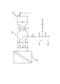
[0014] На фиг. 3 схематично показан предпочтительный вариант осуществления защиты привода GaN от синфазных электромагнитных помех с высоким значением dV/dt согласно настоящему изобретению.[0014] FIG. 3 schematically shows a preferred embodiment of protecting a GaN drive from high dV / dt common mode electromagnetic interference according to the present invention.
[0015] На фиг. 4 на виде сверху показана тепловая карта для примера реализации компонентов инвертора согласно настоящему изобретению, причем самые горячие части расположены в прямом воздушном потоке.[0015] FIG. 4 is a top view showing a heat map for an example implementation of the components of an inverter according to the present invention, the hottest parts being located in direct air flow.
[0016] На фиг. 5 в разрезе по высоте подробно показана структура тепловых пограничных слоев в инверторе согласно одному из вариантов осуществления настоящего изобретения.[0016] FIG. 5, a cross-sectional view along height shows in detail the structure of thermal boundary layers in an inverter according to one embodiment of the present invention.
[0017] На фиг. 6 показано несколько примеров смоделированных теплоотводов, пригодных для использования в настоящем изобретении.[0017] FIG. 6 shows several examples of simulated heat sinks suitable for use in the present invention.
Осуществление изобретенияThe implementation of the invention
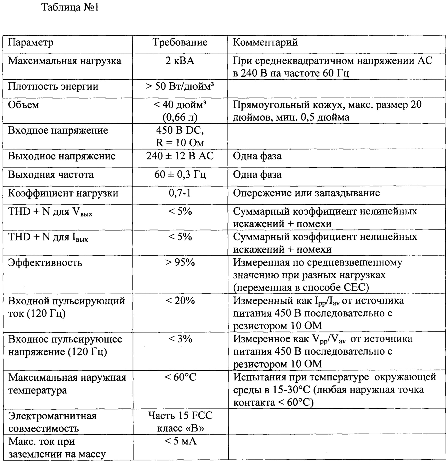
[0018] Согласно одному из вариантов осуществления настоящего изобретения, предлагаемый инвертор сконфигурирован так, чтобы соответствовать требованиям, изложенным в Таблице №1.[0018] According to one embodiment of the present invention, the proposed inverter is configured to meet the requirements set forth in Table No. 1.
[0019] Таким образом, ключевыми факторами, способствующими достижению такой высокой удельной мощности, являются транзисторы из GaN, работающие в так называемом режиме мягкого переключения или в режиме переключения при нулевом напряжении (ZVC, Zero Voltage Switching), объединенные с конкретной топологией с параллельными активными фильтрами и с использованием многослойных керамических конденсаторов (MLCC) в качестве накопительных компонентов. Форма теплоотвода, геометрическая компоновка керамических конденсаторов и оптимизация тепловых пограничных слоев также способствуют получению низкой температуры устройства во время функционирования на полной нагрузке. Оптимизированная работа программного обеспечения в быстром микропроцессоре, связанном со специализированной логической схемой (сложной программируемой логической интегральной схемой (CPLD)), обеспечивает возможность работы в режиме ZVC на протяжении всего рабочего диапазона и уменьшает электромагнитный шум. Благодаря двойному экрану и оптимизированному набору фильтров инвертор может соответствовать требованиям электромагнитной совместимости.[0019] Thus, the key factors contributing to the achievement of such a high specific power are GaN transistors operating in the so-called soft switching mode or in zero voltage switching mode (ZVC, Zero Voltage Switching), combined with a specific topology with parallel active filters and using multilayer ceramic capacitors (MLCC) as storage components. The shape of the heat sink, the geometric arrangement of ceramic capacitors and the optimization of thermal boundary layers also contribute to the low temperature of the device during operation at full load. Optimized software operation in a fast microprocessor associated with a specialized logic circuit (complex programmable logic integrated circuit (CPLD)) provides the ability to work in ZVC mode throughout the entire operating range and reduces electromagnetic noise. Thanks to the double screen and optimized filter set, the inverter can meet the requirements of electromagnetic compatibility.
Предпочтительные варианты осуществления изобретенияPreferred Embodiments
[0020] К применяемым методам конструирования относятся: точное определение размеров с аналитическими вычислениями и моделирование по методу конечных элементов; использование имитационных моделей, полученных с помощью симулятора электронных схем общего назначения с открытым кодом (SPICE), для питания и управления; трехмерное механическое моделирование и использование имитаций тепловых условий, что позволило создать инверторное устройство, отвечающее всем требованиям, изложенным в таблице №1, за один прогон вычислительной программы.[0020] Design methods used include: accurate sizing with analytical calculations and finite element modeling; the use of simulation models obtained using the simulator of electronic circuits of general purpose open source (SPICE), for power and control; three-dimensional mechanical modeling and the use of simulated thermal conditions, which allowed us to create an inverter device that meets all the requirements set forth in table No. 1, for one run of the computing program.
[0021] Согласно одному из предпочтительных вариантов осуществления настоящего изобретения, использование технологии на основе GaN позволяет получить удельную мощность примерно в 143 Вт/дюйм3 для инвертора при 2 кВА, спроектированного согласно настоящему изобретению. Его размеры составляют приблизительно 2,5*1,6*3,5 дюймов, что соответствует объему примерно в 14 дюйм3 (или 0,2 л).[0021] According to one preferred embodiment of the present invention, the use of GaN-based technology provides a power density of about 143 W / in 3 for a 2 kVA inverter designed according to the present invention. Its dimensions are approximately 2.5 * 1.6 * 3.5 inches, which corresponds to a volume of approximately 14 inches 3 (or 0.2 l).
[0022] Транзисторы из GaN имеют высокоэффективные электрические характеристики (низкое Rds_on, низкие Qgate и Cds, сверхнизкое Qrr). Эти характеристики, очевидно, обеспечивают технологические преимущества по сравнению с используемыми в настоящее время и вошедшими в повседневную практику устройствами на полевых транзисторах с изолированным затвором (MOSFET, Metal Oxide Semiconductor Field Effect Transistor) и устройствами на биполярных транзисторах с изолированным затвором (IGBT, Insulated Gate Bipolar Transistor), причем и те, и другие имеют небольшие размеры и низкие производственные затраты. К сожалению, они также имеют серьезные недостатки, обусловленные их очень высокими параметрами переключения (например, сверхвысоким значением dV/dt): довольно сложно обеспечить их привод, а также они требуют чувствительного управления уровнем электромагнитного шума. Другой недостаток заключается в высоком падении напряжения из-за обратного тока, возникающего при выключении транзисторов из GaN. Одно из решений, направленных на устранение указанных недостатков и выбранных в настоящем изобретении, заключается в управлении всеми транзисторами из GaN с использованием мягкого переключения (или режима ZVS) в течение всего рабочего диапазона.[0022] GaN transistors have high performance electrical characteristics (low R ds_on , low Q gate and C ds , ultra low Q rr ). These characteristics obviously provide technological advantages over currently used and commonly used insulated gate devices (MOSFETs, Metal Oxide Semiconductor Field Effect Transistors) and insulated gate bipolar transistors (IGBTs, Insulated Gate Bipolar Transistor), both of which are small and have low manufacturing costs. Unfortunately, they also have serious drawbacks due to their very high switching parameters (for example, ultra-high dV / dt): it is quite difficult to provide their drive, and they also require sensitive control of the level of electromagnetic noise. Another disadvantage is the high voltage drop due to the reverse current that occurs when the transistors from GaN are turned off. One solution to address these drawbacks and selected in the present invention is to control all transistors from GaN using soft switching (or ZVS mode) throughout the entire operating range.
[0023] Для объединения постоянного тока на входной ступени 450 В и переменного выходного напряжения в 240 В, выбирают инвертор 1 с топологией с по меньшей мере тремя плечами (полная мостовая топология или топология с двумя плечами с резервным активным фильтром). Предпочтительно, в предпочтительном варианте осуществления, показанном на фиг. 2, выбрана топология с пятью плечами, поскольку она сводит к минимуму передачу энергии внутри инвертора. Соответственно, каждый полумост, а именно первый полумост и второй полумост, предпочтительно разделен с помощью дополнительного полумоста, установленного на нем параллельно. Это позволяет сглаживать высокий ток и небольшие разности по времени переключения.[0023] To combine the direct current at the 450 V input stage and the alternating 240 V output voltage, an
Два полумоста 201 (НВ, Half Bridge) создают линейное напряжение, два других полумоста 202 создают нейтральное напряжение, а последний полумост 203 используется в качестве вышеупомянутого активного фильтра.Two half-bridges 201 (HB, Half Bridge) create a linear voltage, two other half-
[0024] Согласно рассматриваемому предпочтительному варианту осуществления (см. также фиг. 2) индукторы с L1 по L6 рассчитаны на диапазон от 10 мкГн до 50 мкГн. Благодаря активному фильтру 203 (с C5/L6), входной конденсатор С1 доведен до емкости менее 15 мкФ, а С5 рассчитан на емкость менее 150 мкФ. Синфазные индукторы (L7-L16, см. перевернутый символ «С») рассчитаны на диапазон от 200 мкГн до 1 мГн. Общий коэффициент соответствующих конденсаторов Y-типа (С7, С8, С10-С17, С21, С22) превышает 500 нФ, с сохранением остаточных токов ниже допустимого значения (изначально 5 мА), поскольку выходная синусоидальная волна является симметричной между L+ и L-, то есть (VL + VN)/2 ~= (VL+ + VL-)/2 ~= VЗемля с конфигурацией заземления с расщепленными фазами, и гасит остаточный ток, а также поскольку некоторые конденсаторы Y-типа (С7, С8) замыкаются на землю. Противофазные ЕМС-индукторы (L17-L22, см., символ «Z») рассчитаны на диапазон от 10 мкГн до 20 мкГн, а конденсаторы Х-типа (С2, С6, С9, С18-С20) работают в диапазоне от 1 мкФ до 5 мкФ.[0024] According to a preferred embodiment under consideration (see also FIG. 2), L1 to L6 inductors are designed for a range of 10 μH to 50 μH. Thanks to the active filter 203 (with C5 / L6), the input capacitor C1 is brought to a capacitance of less than 15 microfarads, and C5 is designed for a capacitance of less than 150 microfarads. Common-mode inductors (L7-L16, see the inverted symbol "C") are designed for a range from 200 μH to 1 mH. The total coefficient of the corresponding Y-type capacitors (C7, C8, C10-C17, C21, C22) exceeds 500 nF, while maintaining the residual currents below the permissible value (initially 5 mA), since the output sine wave is symmetrical between L + and L-, then there is (V L + V N ) / 2 ~ = (V L + + V L- ) / 2 ~ = V Earth with a ground configuration with split phases, and damps the residual current, as well as some Y-type capacitors (C7, C8 ) close to the ground. Antiphase EMC inductors (L17-L22, see, the symbol "Z") are designed for a range from 10 μH to 20 μH, and X-type capacitors (C2, C6, C9, C18-C20) operate in the range from 1 μF to 5 uF.
[0025] Высокая удельная мощность и высокая эффективность данного инвертора обусловлены оптимизированным управлением пяти плеч посредством переключения. Для нагрузки любого типа, такое управление обеспечит функционирование с мягким переключением всех устройств из GaN и позволит свести к минимуму обратные токи во время простоев. Алгоритм управления гарантирует, что модуль оказывается естественным образом защищенным от перезагрузки по току. Во время фазы отладки, авторы настоящего изобретения столкнулись с рядом проблем, связанных с тем, что алгоритм управления требует высокой вычислительной нагрузки. В результате, процессор был обновлен с помощью поэлементно совместимой модели, скорость которой на 40% выше.[0025] The high power density and high efficiency of this inverter are due to optimized five-arm control by switching. For any type of load, this control will provide a soft-switching operation for all devices from GaN and will minimize reverse currents during downtime. The control algorithm ensures that the module is naturally protected against overcurrent. During the debug phase, the authors of the present invention encountered a number of problems associated with the fact that the control algorithm requires high computational load. As a result, the processor was updated using an element-wise compatible model, whose speed is 40% higher.
[0026] Цели управления достигнуты за счет применения следующих принципов:[0026] The management objectives are achieved through the application of the following principles:
цифровое управление, основанное на быстром микроконтроллере, объединенном со специализированной логической схемой (CPLD);digital control based on a fast microcontroller combined with specialized logic circuit (CPLD);
быстрое измерение входных/выходных токов и напряжений;fast measurement of input / output currents and voltages;
эффективная обратная связь на события переключения полумостов;effective feedback on half-bridge switching events;
алгоритм обучения для приведения в действие активного фильтра;learning algorithm for driving an active filter;
оптимизация частоты переключения между 35 и 240 кГц в зависимости от выходного тока; регулируемый фазовый сдвиг между полумостами (0° или 90°) и модуляция времени простоя пяти полумостов (от 50 нс до 3 мкс). Таким образом, потери от переключения почти исключены, а увеличение частоты способствует оптимизации (уменьшению) размера пассивных компонентов.optimization of the switching frequency between 35 and 240 kHz depending on the output current; adjustable phase shift between half-bridges (0 ° or 90 °) and modulation of the downtime of five half-bridges (from 50 ns to 3 μs). Thus, switching losses are almost eliminated, and an increase in frequency helps to optimize (reduce) the size of passive components.
[0027] Применение фазового сдвига между нейтральными и линейными полумостами (2 или 4, соответственно) является обязательным, поскольку фильтрующие индукторы DMN оптимизированы при нулевом фазовом сдвиге. Таким образом, мягкое переключение больше не происходит в каждом переключателе из GaN. Кроме того, поскольку переключение осуществляется при сверхвысокой скорости, и с некоторой неопределенностью в отношении тока, протекающего в фильтрующих индукторах DMN, следующее переключение тока может произойти при значении тока, которое (еще) не обнулилось, что приводит к режиму «без ZVS». Найденное решение для обеспечения приближения тока к нулевому значению состоит в увеличении времени простоя переключателя (не показано).[0027] The use of a phase shift between neutral and linear half-bridges (2 or 4, respectively) is mandatory because the DMN filter inductors are optimized for a zero phase shift. Thus, soft switching no longer occurs in every GaN switch. In addition, since the switching is carried out at an ultrahigh speed, and with some uncertainty regarding the current flowing in the DMN filter inductors, the next switching of the current can occur at a value of the current that has not yet reset, which leads to the “without ZVS” mode. The solution found to ensure that the current approaches zero is to increase the downtime of the switch (not shown).
[0028] Благодаря высокоскоростному переключению в предлагаемом преобразователе, согласно одному из вариантов осуществления настоящего изобретения, выполняют не измерение постоянного тока, а за счет использования емкостного делителя 301 напряжения (С33, С34) выявляют, когда ток стремится к нулю (см. фиг. 3). Благодаря соответствующему выбору конденсаторов, такой емкостный делитель позволяет процессору управлять измерением допустимого напряжения (как правило, примерно 5 В вместо максимального пикового напряжения в 450 В).[0028] Due to the high-speed switching in the proposed converter, according to one embodiment of the present invention, it is not a direct current measurement that is performed, but due to the use of a capacitive voltage divider 301 (C33, C34), it is detected when the current tends to zero (see Fig. 3 ) Thanks to the appropriate choice of capacitors, such a capacitive divider allows the processor to control the measurement of permissible voltage (usually about 5 V instead of the maximum peak voltage of 450 V).
[0029] В настоящем изобретении устойчивость управления GaN является критическим параметром. На самом деле, транзисторы из GaN переключаются очень быстро, так что они обеспечивают высокое значение dV/dt при отключении управления, далеко за пределами допустимых значений для большинства приводов, имеющихся в настоящее время в продаже. Кроме того, пороговое значение напряжения управления является очень низким. Более того, согласно настоящему изобретению, была разработана очень компактная, недорогая и чрезвычайно устойчивая схема привода, которая способна приводить в действие транзисторы из GaN в их нормативных пределах (см. фиг. 3). Согласно варианту осуществления, проиллюстрированному на фиг. 3, используют дополнительный источник и затворные катушки индуктивности (L31, L32) для устранения CMN, проходящего в транзисторах из GaN непосредственно в землю, без влияния на привод 303 из GaN. Для этого расположен CMN-фильтр 302 (L31, С31, L32, С32).[0029] In the present invention, the stability of GaN control is a critical parameter. In fact, GaN transistors switch very quickly, so that they provide a high dV / dt when the control is turned off, well beyond the permissible values for most drives currently on sale. In addition, the threshold value of the control voltage is very low. Moreover, according to the present invention, a very compact, inexpensive and extremely stable drive circuit has been developed which is capable of driving transistors from GaN within their standard limits (see FIG. 3). According to the embodiment illustrated in FIG. 3, use an additional source and gate inductors (L31, L32) to eliminate the CMN passing in the transistors from GaN directly to the ground, without affecting the
[0030] Выбор правильного корпуса GaN также играет важную роль. Согласно одному из вариантов осуществления, для такого проектного решения наилучшим выбором оказалась модель для поверхностного монтажа (SMD) с доступом к двум источникам, один из которых предназначен для обеспечения электропитания, а другой - для подачи команды. Это обеспечивает безопасное управление транзистором. Кроме того, небольшой корпус снижает индукционные помехи и, следовательно, функциональное электрическое перенапряжение. Разводка печатной платы и расположение разделяющих конденсаторов играют важнейшую роль для надлежащего функционирования компонентов из GaN.[0030] Choosing the right GaN package also plays an important role. According to one embodiment, for such a design solution, the best choice was a surface mount model (SMD) with access to two sources, one of which is designed to provide power and the other to give a command. This provides safe transistor control. In addition, a small housing reduces inductive interference and, therefore, functional electrical overvoltage. PCB layout and isolation capacitors play a critical role in the proper functioning of GaN components.
Входной ток частотой 120 Гц и требование пульсации напряжения/тока120 Hz input current and voltage / current ripple requirement
[0031] Для того чтобы удовлетворить требование пульсации на входе напряжения DC/тока, был разработан параллельный активный фильтр, который может компенсировать пульсацию более эффективно, чем в случае использования большого конденсатора на стороне входа. Принятое решение также является более надежным по сравнению с использованием топологии, основанной на «повышении напряжения», для которой рабочие напряжения могут повышаться до предельного Vмакс транзисторов из GaN.[0031] In order to satisfy the ripple requirement of the DC voltage / current input, a parallel active filter has been developed that can compensate for ripple more efficiently than with a large capacitor on the input side. The decision made is also more reliable in comparison with the use of a topology based on “voltage increase”, for which the operating voltage can increase to the maximum V max of GaN transistors.
[0032] Активный фильтр работает с более высокими перепадами напряжения (примерно 200 Vpk-pk) и сохраняет соответствующую энергию в керамических конденсаторах, емкость которых возрастает при уменьшении напряжения, что приводит к трем преимуществам:[0032] An active filter operates with higher voltage drops (approximately 200 V pk-pk ) and stores the corresponding energy in ceramic capacitors, the capacitance of which increases with decreasing voltage, which leads to three advantages:
уменьшение размера входного конденсатора С1 параллельного резонансного контура (менее 15 мкФ);reducing the size of the input capacitor C1 parallel resonant circuit (less than 15 microfarads);
уменьшение размера фильтрующего конденсатора С5 до величины менее 150 мкФ;reducing the size of the filter capacitor C5 to less than 150 microfarads;
устойчивость инвертора благодаря использованию компонентов из GaN ниже 450 Vdc.inverter stability due to use of GaN components below 450 V dc .
[0033] Программное обеспечение также способствует этому; алгоритм сохраняет Vвх постоянным и обеспечивает возможность более крупных пульсаций в активном фильтре. Кроме того, алгоритм обучения также уменьшает входные пульсации (на 3 порядка) за счет исправления ошибок моделирования благодаря наличию периодов простоя.[0033] The software also contributes to this; the algorithm keeps V input constant and allows larger ripple in the active filter. In addition, the learning algorithm also reduces input ripple (by 3 orders of magnitude) by correcting modeling errors due to the presence of downtime.
Миниатюризация компонентов для преобразования постоянного тока в переменныйMiniaturization of components for converting DC to AC
[0034] Согласно одному из вариантов осуществления настоящего изобретения, использование MLCC-конденсаторов (то есть, керамических конденсаторов) для сохранения энергии обеспечивает получение более компактного и эффективного модуля.[0034] According to one embodiment of the present invention, the use of MLCC capacitors (that is, ceramic capacitors) for energy conservation provides a more compact and efficient module.
[0035] Кроме того, магнитные компоненты, в основном, состоят из феррита, причем известно, что их магнитные потери являются очень низкими при высоких частотах. Использование литцендрата сводит к минимуму потери благодаря поверхностному эффекту и эффекту близости. Для дальнейшей минимизации, провода наматывают непосредственно на феррит, без каркаса для намотки катушки. Их охлаждение осуществляется посредством воздушного потока вентилятора и за счет использования фольги из оксида алюминия, расположенной в середине феррита для создания требуемого воздушного зазора и теплового отвода. Размер фильтрующих конденсаторов и индукторов оптимизирован благодаря увеличению допустимого пульсирующего тока.[0035] Furthermore, the magnetic components are mainly composed of ferrite, and it is known that their magnetic losses are very low at high frequencies. The use of litzendrat minimizes losses due to the surface effect and proximity effect. To further minimize, wires are wound directly onto ferrite, without a frame for winding a coil. Their cooling is carried out through the air flow of the fan and through the use of aluminum oxide foil located in the middle of the ferrite to create the required air gap and heat dissipation. The size of the filtering capacitors and inductors is optimized by increasing the permissible ripple current.
[0036] Что касается выходного тока, то датчик Холла с разомкнутой петлей, объединенный с электромагнитным экраном, обеспечивает получение очень компактного измерительного устройства, предоставляющего гальваническую развязку и уменьшение чувствительности к синфазному и индукционному шуму. Время его срабатывания является очень малым, что способствует защите инвертора от короткого замыкания или высоких ударов нагрузки.[0036] As for the output current, the open-loop Hall sensor, combined with an electromagnetic screen, provides a very compact measuring device that provides galvanic isolation and reduces sensitivity to common mode and induction noise. Its response time is very short, which helps protect the inverter from short circuit or high impact shocks.
[0037] Следует отметить, что все другие результаты оценки тока (Iиндуктор, и т.д.) получены благодаря наблюдателям состояния без датчиков тока (бессенсорное измерение, например, напряжений), что снижает габаритный размер инвертора.[0037] It should be noted that all other current estimation results (I inductor , etc.) were obtained thanks to state observers without current sensors (sensorless measurement, for example, voltages), which reduces the overall size of the inverter.
[0038] Благодаря особой модуляции по управлению компонентов из GaN, которая уменьшает ток в фильтрующих индукторах L7-L8 (см., фиг. 2), размер их сердечника уменьшается без достижения уровня насыщения.[0038] Due to the special modulation for controlling components from GaN, which reduces the current in the filtering inductors L7-L8 (see, Fig. 2), their core size decreases without reaching the saturation level.
[0039] Обеспечение слоистой структуры для всех печатных плат и теплоотвода представляет собой серьезную трудность. Как показано на фиг. 5, она была получена за счет использования микропружинных контактов 507, специального теплоотвода 512, изготовленного посредством электроимпульсной обработки (EDM, Electrical Discharge Machining), ультратонких печатных плат 510, 513, и т.д. (толщиной 0,012 дюйма), силиконового пенопласта 508 для распределения контактного давления компонентов из GaN на теплоотвод 512. Все эти технические признаки в значительной степени способствовали уменьшению размера инвертора.[0039] Providing a layered structure for all printed circuit boards and heat sinks is a serious challenge. As shown in FIG. 5, it was obtained through the use of
[0040] Согласно одному из вариантов осуществления, инверторный модуль содержит, в основном, две части. Первая часть включает в себя управление устройством, вспомогательный источник питания, плечи (или полумосты) в количестве пяти штук и их соответствующие приводы совместно с теплоотводом. Вторая часть включает в себя пассивные фильтры.[0040] According to one embodiment, the inverter module comprises mainly two parts. The first part includes control of the device, an auxiliary power source, shoulders (or half-bridges) in the amount of five pieces and their respective drives together with the heat sink. The second part includes passive filters.
[0041] Предпочтительно, резонансная топология мягкого переключения LLC использована для изолированного вспомогательного источника питания 12 В/5 В/3,3 В (примерно 10 Вт). Это позволяет уменьшить его объем до величины менее 0,128 дюйм3 (0,8*0,8*0,2 дюймов), что, в свою очередь, обеспечивает возможность надлежащей интеграции внутри упомянутой выше управляющей части на единственной печатной плате.[0041] Preferably, the LLC resonant soft switching topology is used for an isolated auxiliary power supply of 12 V / 5 V / 3.3 V (about 10 W). This makes it possible to reduce its volume to less than 0.128 inch 3 (0.8 * 0.8 * 0.2 inch), which, in turn, allows proper integration within the control part mentioned above on a single printed circuit board.
Управление тепловым процессомThermal management
[0042] С учетом оцененных и моделируемых потерь, принудительное воздушное охлаждение является единственным эффективным решением, способным в достаточной степени уменьшить тепловое сопротивление до окружающего воздуха. Согласно одному из вариантов осуществления, эффективный осевой вентилятор (примерные размеры 1,57*1,57*0,6 дюймов) расположен в середине передней пластины.[0042] Given the estimated and simulated losses, forced air cooling is the only effective solution that can sufficiently reduce thermal resistance to ambient air. According to one embodiment, an effective axial fan (approximate dimensions 1.57 * 1.57 * 0.6 inches) is located in the middle of the front plate.
[0043] Карта теплового моделирования с фиг. 4 демонстрирует результат, когда все компоненты оптимальным образом расположены вокруг вентилятора, а именно:[0043] The thermal simulation map of FIG. 4 shows the result when all components are optimally positioned around the fan, namely:
самые горячие компоненты находятся в прямом воздушном потоке;the hottest components are in direct airflow;
площади теплообменной поверхности увеличены до максимума;heat transfer surface areas are increased to a maximum;
потери давления сведены к минимуму;pressure loss is minimized;
скорость воздуха рядом с боковой стороной оптимизирована иthe air speed near the side is optimized and
вход свежего воздуха рядом с теплоотводом из GaN сводит к минимуму тепловое сопротивление, что повышает до максимума эффективность инвертора.fresh air inlet near the GaN heat sink minimizes thermal resistance, which maximizes inverter efficiency.
[0044] Таким образом, выбор подходящих тепловых пограничных слоев имеет решающее значение для уменьшения мест локального перегрева на наружной поверхности инвертора. На фиг. 5 показана тепловая многоуровневая или слоистая структура согласно одному из вариантов осуществления (вид в разрезе по высоте). Температура перехода GaN не превышает 60° при температуре окружающей среды в 30°С и нагрузке 2 кВт.[0044] Thus, the selection of suitable thermal boundary layers is critical to reducing local overheating on the outer surface of the inverter. In FIG. 5 shows a thermal multilevel or layered structure according to one embodiment (sectional view in height). The GaN transition temperature does not exceed 60 ° at an ambient temperature of 30 ° C and a load of 2 kW.
[0045] На фиг. 5 показана подробная структура тепловых пограничных слоев согласно одному из вариантов осуществления. Для одного транзистора 509 из GaN (потери примерно 2 Вт), тепловые сопротивления имеют следующий вид:[0045] FIG. 5 shows a detailed structure of thermal boundary layers according to one embodiment. For a
переход GaN - тепловая прокладка: 0,5°С/Вт;GaN transition - thermal padding: 0.5 ° C / W;
конструкция печатной платы 510, увеличивающая перенос тепла от транзистора 509 из GaN к теплоотводу 512: 1,1°С/Вт;the design of the printed
термопаста с пылью из оксида алюминия: 0,3°С/Вт;thermal grease with aluminum oxide dust: 0.3 ° C / W;
керамическая теплоизоляционная фольга с нитридом алюминия 511: 0,02°С/Вт;ceramic thermal insulation foil with aluminum nitride 511: 0.02 ° C / W;
теплопроводящий клей с серебряной пылью: 0,15°С/Вт иsilver dust heat transfer adhesive: 0.15 ° C / W and
ячеистый теплоотвод 512 с принудительно подаваемым воздухом (см. ниже): 13°С/Вт (относительно единственного компонента из GaN).512 mesh heat sink with forced air (see below): 13 ° C / W (relative to a single GaN component).
[0046] И наружный экран 501, 503, и теплоотвод 512 изготовлены из меди, а накопительные конденсаторы 514 представляют собой керамические MLCC. Оба материала выбраны для повышения теплового потока и площади теплообменной поверхности. Узел конденсаторов, образующий активный фильтр, представляет собой устройство накопления энергии, но также является продолжением теплоотвода 512. Воздушный поток между каждым рядом из MLCC (предпочтительно с зазором ± 0,04 дюйма или 1 мм между конденсаторами) повышает охлаждающий эффект, поскольку конденсаторы играют роль ребер. Объем, занимаемый накопителем энергии, выступает в качестве второго теплоотвода, благодаря геометрической форме узла и типу конденсатора (хороший проводник тепла).[0046] Both the
[0047] Несколько типов теплоотводов, показанных на фиг. 6, термически смоделировали и сравнили с упомянутой выше трехмерной моделью (множество дисков 601, ячеистая структура 602, ребра с чередованием 603 или нет, медный пенопласт 604 и т.д.).[0047] Several types of heat sinks shown in FIG. 6, thermally simulated and compared with the above three-dimensional model (a plurality of
[0048] Предпочтительно, был выбран ячеистый теплоотвод 602 (Rth_total = 1,3°С/Вт (10 GaN); L2,79*W0,83*H0,26 дюймов), поскольку он сводит к минимуму температуру GaN и имеет отверстия, достаточно большие для того, чтобы избежать закупорки пылью. Двухмерная структура распределяет по поверхности температуру и дополнительно уменьшает количество мест локального перегрева.[0048] Preferably, a mesh heat sink of 602 (Rth_total = 1.3 ° C / W (10 GaN); L2.79 * W0.83 * H0.26 inches) was selected because it minimizes the temperature of the GaN and has openings, Large enough to avoid dust clogging. The two-dimensional structure distributes the temperature on the surface and further reduces the number of places of local overheating.
[0049] Несколько индукторов 504 (но не все из них) предпочтительно термически прикреплены к медному экрану 503. Для того чтобы наружный корпус соответствовал предельно допустимому температурному режиму в 60°С, прокладка 502 обеспечивает электроизоляционный, но теплопроводящий пограничный слой между экраном 503 и наружным корпусом 501. Таким образом, тепловое сопротивление пограничного слоя способствует отведению тепла из самых горячих внутренних компонентов и предотвращает рассеивание этого тепла локально наружным корпусом.[0049] Several inductors 504 (but not all of them) are preferably thermally attached to the
Электромагнитная совместимость (EMC, Electromagnetic Compliance)Electromagnetic compatibility (EMC)
[0050] Для того чтобы обеспечить удовлетворение требований, относящихся к части 15 правил Федеральной комиссии по связи (FCC, Federal Communications Commission) класса «В» (для бытового оборудования, который является более жестким по сравнению с классом «А», для коммерческого или промышленного оборудования), выбор топологии и тип модуляции был основан на моделях источников шума. Каждый фильтр был смоделирован на установленной модели шума для оптимизации конструкции инвертора и разводки печатной платы. Ключевые факторы согласно настоящему изобретению для удовлетворения требований класса «В» можно суммировать следующим образом:[0050] In order to satisfy the requirements of Part 15 of the rules of the Federal Communications Commission (FCC) Class “B” (for household equipment that is more stringent than Class “A”, for commercial or industrial equipment), the choice of topology and type of modulation was based on models of noise sources. Each filter was modeled on an installed noise model to optimize the inverter design and PCB layout. The key factors according to the present invention to meet the requirements of class "B" can be summarized as follows:
Мягкое переключение основных переключателей и вспомогательного источника питания независимо от нагрузки;Soft switching of the main switches and auxiliary power supply regardless of the load;
регулируемая частота и особая спектральная модуляция;adjustable frequency and special spectral modulation;
первый внутренний экран, электрически соединенный с (L- = О В DC);a first inner shield electrically connected to (L- = 0 V DC);
второй экран (наружный корпус) и экран последней фильтрующей ступени;the second screen (outer casing) and the screen of the last filter stage;
фильтр выходного переменного тока (АСвых), связанный с (L-);an AC output filter (AC output ) associated with (L-);
использование нескольких небольших фильтров вместо одного большого;use of several small filters instead of one large;
подавление всех резонирующих полюсов на частотах выше 50 кГц;suppression of all resonant poles at frequencies above 50 kHz;
использование керамических конденсаторов для сведения к минимуму индукционные помехи и их размера;the use of ceramic capacitors to minimize induction noise and their size;
сведение к минимуму связи между фильтрами;Minimizing communication between filters
сведение к минимуму емкостной связи в конструкции индуктора.minimizing capacitive coupling in the design of the inductor.
Перечень ссылочных обозначенийReference List
100 Фильтр синфазного шума100 Common Mode Filter
101 Фильтр противофазного шума101 Antiphase noise filter
201 Полумост линейного выключателя201 Half bridge linear switch
202 Полумост переключателя нейтрали202 Half bridge neutral switch
203 Полумост активного фильтра203 Half bridge active filter
204 Заземленный экран или соединение на землю204 Grounded shield or ground connection
301 Емкостный делитель для выявления перехода через нулевой ток301 Capacitive divider for detecting zero current crossover
302 CMN-фильтр для переключателя GaN без подвижных частей302 CMN filter for GaN switch without moving parts
303 Привод GaN303 GaN Drive
501 Медный корпус501 Copper Case
502 Изоляционный/тепловой пограничный слой502 Insulation / thermal boundary layer
503 Медный экран503 copper screen
504 Индуктор(ы)504 Inductor (s)
505 Зазор керамического индуктора505 Ceramic Inductor Clearance
506 Внутреннее соединение печатной платы506 Internal circuit board connection
507 Микропружинные контакты507 Micro spring contacts
508 Кремнийорганический пенопласт508 Silicone Foam
509 Переключатель GaN509 GaN switch
510 Печатная плата с тепловыми сквозными перемычками510 Circuit board with thermal through jumpers
511 Керамическая изоляция511 Ceramic Insulation
512 Ячеистый теплоотвод512 Cellular Heat Sink
513 Печатная плата для установки накопительных конденсаторов513 Circuit board for the installation of storage capacitors
514 Керамический активный фильтрующий конденсатор514 Ceramic Active Filter Capacitor
601 Многодисковый теплоотвод601 multi-disc heat sink
602 Ячеистый теплоотвод602 Cellular Heat Sink
603 Теплоотвод с чередующимися ребрами603 Heatsink with alternating fins
604 Теплоотвод из медного пенопласта604 Copper foam heat sink
Claims (16)
Applications Claiming Priority (5)
| Application Number | Priority Date | Filing Date | Title |
|---|---|---|---|
| EP15176078 | 2015-07-09 | ||
| EP15176078.2 | 2015-07-09 | ||
| EP15195518.4 | 2015-11-20 | ||
| EP15195518.4A EP3171684B1 (en) | 2015-11-20 | 2015-11-20 | High power density inverter (ii) |
| PCT/EP2016/064615 WO2017005505A1 (en) | 2015-07-09 | 2016-06-23 | High power density inverter (ii) |
Publications (3)
| Publication Number | Publication Date |
|---|---|
| RU2018104099A RU2018104099A (en) | 2019-08-09 |
| RU2018104099A3 RU2018104099A3 (en) | 2019-08-29 |
| RU2702103C2 true RU2702103C2 (en) | 2019-10-04 |
Family
ID=56203389
Family Applications (1)
| Application Number | Title | Priority Date | Filing Date |
|---|---|---|---|
| RU2018104099A RU2702103C2 (en) | 2015-07-09 | 2016-06-23 | Inverter with high specific power |
Country Status (4)
| Country | Link |
|---|---|
| US (1) | US10312801B2 (en) |
| CN (1) | CN107852840B (en) |
| RU (1) | RU2702103C2 (en) |
| WO (1) | WO2017005505A1 (en) |
Families Citing this family (8)
| Publication number | Priority date | Publication date | Assignee | Title |
|---|---|---|---|---|
| CN109496057A (en) * | 2018-11-12 | 2019-03-19 | 晶晨半导体(上海)股份有限公司 | A kind of printed circuit board layout |
| US10630164B1 (en) * | 2019-02-08 | 2020-04-21 | Hamilton Sundstrand Corporation | Generator systems |
| CN110474525A (en) * | 2019-08-21 | 2019-11-19 | 北京华商三优新能源科技有限公司 | Charging unit including silicon carbide charging module |
| CN111511138A (en) * | 2020-04-29 | 2020-08-07 | 四川虹美智能科技有限公司 | Machine cabinet |
| DE102020124822A1 (en) | 2020-05-25 | 2021-11-25 | Infineon Technologies Ag | Electrical inverter system |
| US11742764B2 (en) * | 2021-02-04 | 2023-08-29 | Maxim Integrated Products, Inc. | Resonant power converters including coupled inductors |
| CN116432599B (en) * | 2023-06-12 | 2023-08-08 | 北京智芯仿真科技有限公司 | Method and system for optimizing SINK pins of integrated circuit |
| US12104772B1 (en) | 2024-01-16 | 2024-10-01 | Enova Illuminations, Inc. | Sanitation control for headlamps having variable beam illumination |
Citations (4)
| Publication number | Priority date | Publication date | Assignee | Title |
|---|---|---|---|---|
| EP2149973A2 (en) * | 2008-07-29 | 2010-02-03 | Hitachi Ltd. | Power conversion apparatus and electric vehicle |
| RU2499349C2 (en) * | 2008-03-06 | 2013-11-20 | Конинклейке Филипс Электроникс Н.В. | Unit to control power inverter of dc conversion into ac of circuit of resonant power converter, in particular, dc converter into dc for use in circuits of high voltage generator of up-to-date device of computer tomography or x-ray system |
| EP2675054A1 (en) * | 2011-02-08 | 2013-12-18 | Sanyo Electric Co., Ltd. | Power conditioner |
| EP2879475A1 (en) * | 2013-11-27 | 2015-06-03 | SMA Solar Technology AG | Solar inverter |
Family Cites Families (10)
| Publication number | Priority date | Publication date | Assignee | Title |
|---|---|---|---|---|
| US20060120001A1 (en) * | 2004-12-03 | 2006-06-08 | Weber William J | Modular power supply assembly |
| JP4839096B2 (en) * | 2006-02-13 | 2011-12-14 | 株式会社日立産機システム | Power converter |
| CA2671823C (en) * | 2006-12-07 | 2013-08-06 | Northern Power Systems, Inc. | Modular power converters usable alone or in a multiphase power converter |
| JP5380376B2 (en) * | 2010-06-21 | 2014-01-08 | 日立オートモティブシステムズ株式会社 | Power semiconductor device |
| US9320131B2 (en) | 2010-09-17 | 2016-04-19 | Intervention Technology Pty Ltd | Power supply device and components thereof |
| US9071141B2 (en) * | 2011-04-08 | 2015-06-30 | Virginia Tech Intellectual Properties, Inc. | Two-stage single phase bi-directional PWM power converter with DC link capacitor reduction |
| US9030822B2 (en) * | 2011-08-15 | 2015-05-12 | Lear Corporation | Power module cooling system |
| US9048756B2 (en) * | 2012-03-07 | 2015-06-02 | Virginia Tech Intellectual Properties, Inc. | DC-side leakage current reduction for single phase full-bridge power converter/inverter |
| WO2015089279A1 (en) * | 2013-12-11 | 2015-06-18 | Rompower Energy Systems Inc. | Packaging method for very high density converters |
| WO2015142375A1 (en) * | 2014-03-21 | 2015-09-24 | Robert Bosch Gmbh | Common mode noise suppression of switch-mode power converters by capacitive shield with damping network |
-
2016
- 2016-06-23 US US15/743,054 patent/US10312801B2/en active Active
- 2016-06-23 CN CN201680040361.6A patent/CN107852840B/en not_active Expired - Fee Related
- 2016-06-23 WO PCT/EP2016/064615 patent/WO2017005505A1/en not_active Ceased
- 2016-06-23 RU RU2018104099A patent/RU2702103C2/en not_active IP Right Cessation
Patent Citations (4)
| Publication number | Priority date | Publication date | Assignee | Title |
|---|---|---|---|---|
| RU2499349C2 (en) * | 2008-03-06 | 2013-11-20 | Конинклейке Филипс Электроникс Н.В. | Unit to control power inverter of dc conversion into ac of circuit of resonant power converter, in particular, dc converter into dc for use in circuits of high voltage generator of up-to-date device of computer tomography or x-ray system |
| EP2149973A2 (en) * | 2008-07-29 | 2010-02-03 | Hitachi Ltd. | Power conversion apparatus and electric vehicle |
| EP2675054A1 (en) * | 2011-02-08 | 2013-12-18 | Sanyo Electric Co., Ltd. | Power conditioner |
| EP2879475A1 (en) * | 2013-11-27 | 2015-06-03 | SMA Solar Technology AG | Solar inverter |
Also Published As
| Publication number | Publication date |
|---|---|
| RU2018104099A3 (en) | 2019-08-29 |
| US20180205314A1 (en) | 2018-07-19 |
| CN107852840A (en) | 2018-03-27 |
| RU2018104099A (en) | 2019-08-09 |
| CN107852840B (en) | 2019-07-26 |
| WO2017005505A1 (en) | 2017-01-12 |
| US10312801B2 (en) | 2019-06-04 |
Similar Documents
| Publication | Publication Date | Title |
|---|---|---|
| RU2708638C2 (en) | Inverter with high specific power | |
| RU2702103C2 (en) | Inverter with high specific power | |
| Kim et al. | A damping scheme for switching ringing of full SiC MOSFET by air core PCB circuit | |
| Tiwari et al. | Efficiency and conducted EMI evaluation of a single-phase power factor correction boost converter using state-of-the-art SiC MOSFET and SiC diode | |
| US10256718B2 (en) | Low-inductance half-bridge arrangement | |
| US10404186B2 (en) | Power module systems and methods having reduced common mode capacitive currents and reduced electromagnetic interference | |
| EP3171499A1 (en) | High power density inverter (i) | |
| US9641095B1 (en) | Power converter output stage using heat dissipating bus bars | |
| Dusmez et al. | Designing a 1kW GaN PFC stage with over 99% efficiency and 155W/in 3 power density | |
| CN110798123A (en) | Variable frequency drive system and method for improving common mode interference | |
| Frebel et al. | Transformer-less 2 kW non isolated 400 VDC/230 VAC single stage micro inverter | |
| EP3171684B1 (en) | High power density inverter (ii) | |
| Acharya et al. | A 10‐kV SiC‐MOSFET (Gen‐3) Half‐Bridge Module‐Based Isolated Bidirectional DC–DC Converter Block for Medium‐Voltage High‐Power Applications | |
| JP5482211B2 (en) | Snubber circuit for power converter | |
| Corsaro et al. | EMC design guides for motor control applications | |
| Sato et al. | Development of high power density three-phase inverter | |
| CN117178643A (en) | Circuit components including gallium nitride devices | |
| JP6676888B2 (en) | Power converter | |
| Imaoka et al. | Common mode noise reduction methods used for high power density dc/dc converters | |
| Deng | Electromagnetic heterogeneous integration for high-frequency power conversion | |
| Gupta et al. | A DC planar bus bar of high-frequency power converter with enhanced current distribution | |
| CN202495870U (en) | Modular converter | |
| JP7310188B2 (en) | power converter | |
| Kroics | Design Considerations of Common Mode and Differential Mode EMI Input Filter Based on Planar Ferrite Core | |
| JP6316484B1 (en) | Power converter |
Legal Events
| Date | Code | Title | Description |
|---|---|---|---|
| HZ9A | Changing address for correspondence with an applicant | ||
| MM4A | The patent is invalid due to non-payment of fees |
Effective date: 20200624 |