EP4277036A1 - Antenna structure and wireless communication device - Google Patents
Antenna structure and wireless communication device Download PDFInfo
- Publication number
- EP4277036A1 EP4277036A1 EP22205756.4A EP22205756A EP4277036A1 EP 4277036 A1 EP4277036 A1 EP 4277036A1 EP 22205756 A EP22205756 A EP 22205756A EP 4277036 A1 EP4277036 A1 EP 4277036A1
- Authority
- EP
- European Patent Office
- Prior art keywords
- antenna
- ant
- stage
- antenna elements
- output terminals
- Prior art date
- Legal status (The legal status is an assumption and is not a legal conclusion. Google has not performed a legal analysis and makes no representation as to the accuracy of the status listed.)
- Pending
Links
Images



Classifications
-
- H—ELECTRICITY
- H01—ELECTRIC ELEMENTS
- H01Q—ANTENNAS, i.e. RADIO AERIALS
- H01Q1/00—Details of, or arrangements associated with, antennas
- H01Q1/50—Structural association of antennas with earthing switches, lead-in devices or lightning protectors
-
- H—ELECTRICITY
- H01—ELECTRIC ELEMENTS
- H01Q—ANTENNAS, i.e. RADIO AERIALS
- H01Q3/00—Arrangements for changing or varying the orientation or the shape of the directional pattern of the waves radiated from an antenna or antenna system
- H01Q3/26—Arrangements for changing or varying the orientation or the shape of the directional pattern of the waves radiated from an antenna or antenna system varying the relative phase or relative amplitude of energisation between two or more active radiating elements; varying the distribution of energy across a radiating aperture
-
- H—ELECTRICITY
- H01—ELECTRIC ELEMENTS
- H01Q—ANTENNAS, i.e. RADIO AERIALS
- H01Q21/00—Antenna arrays or systems
- H01Q21/0006—Particular feeding systems
-
- H—ELECTRICITY
- H01—ELECTRIC ELEMENTS
- H01Q—ANTENNAS, i.e. RADIO AERIALS
- H01Q21/00—Antenna arrays or systems
- H01Q21/06—Arrays of individually energised antenna units similarly polarised and spaced apart
- H01Q21/22—Antenna units of the array energised non-uniformly in amplitude or phase, e.g. tapered array or binomial array
-
- H—ELECTRICITY
- H01—ELECTRIC ELEMENTS
- H01Q—ANTENNAS, i.e. RADIO AERIALS
- H01Q21/00—Antenna arrays or systems
- H01Q21/29—Combinations of different interacting antenna units for giving a desired directional characteristic
-
- H—ELECTRICITY
- H01—ELECTRIC ELEMENTS
- H01Q—ANTENNAS, i.e. RADIO AERIALS
- H01Q3/00—Arrangements for changing or varying the orientation or the shape of the directional pattern of the waves radiated from an antenna or antenna system
- H01Q3/26—Arrangements for changing or varying the orientation or the shape of the directional pattern of the waves radiated from an antenna or antenna system varying the relative phase or relative amplitude of energisation between two or more active radiating elements; varying the distribution of energy across a radiating aperture
- H01Q3/28—Arrangements for changing or varying the orientation or the shape of the directional pattern of the waves radiated from an antenna or antenna system varying the relative phase or relative amplitude of energisation between two or more active radiating elements; varying the distribution of energy across a radiating aperture varying the amplitude
-
- H—ELECTRICITY
- H01—ELECTRIC ELEMENTS
- H01Q—ANTENNAS, i.e. RADIO AERIALS
- H01Q3/00—Arrangements for changing or varying the orientation or the shape of the directional pattern of the waves radiated from an antenna or antenna system
- H01Q3/26—Arrangements for changing or varying the orientation or the shape of the directional pattern of the waves radiated from an antenna or antenna system varying the relative phase or relative amplitude of energisation between two or more active radiating elements; varying the distribution of energy across a radiating aperture
- H01Q3/30—Arrangements for changing or varying the orientation or the shape of the directional pattern of the waves radiated from an antenna or antenna system varying the relative phase or relative amplitude of energisation between two or more active radiating elements; varying the distribution of energy across a radiating aperture varying the relative phase between the radiating elements of an array
-
- H—ELECTRICITY
- H01—ELECTRIC ELEMENTS
- H01Q—ANTENNAS, i.e. RADIO AERIALS
- H01Q3/00—Arrangements for changing or varying the orientation or the shape of the directional pattern of the waves radiated from an antenna or antenna system
- H01Q3/26—Arrangements for changing or varying the orientation or the shape of the directional pattern of the waves radiated from an antenna or antenna system varying the relative phase or relative amplitude of energisation between two or more active radiating elements; varying the distribution of energy across a radiating aperture
- H01Q3/30—Arrangements for changing or varying the orientation or the shape of the directional pattern of the waves radiated from an antenna or antenna system varying the relative phase or relative amplitude of energisation between two or more active radiating elements; varying the distribution of energy across a radiating aperture varying the relative phase between the radiating elements of an array
- H01Q3/32—Arrangements for changing or varying the orientation or the shape of the directional pattern of the waves radiated from an antenna or antenna system varying the relative phase or relative amplitude of energisation between two or more active radiating elements; varying the distribution of energy across a radiating aperture varying the relative phase between the radiating elements of an array by mechanical means
-
- H—ELECTRICITY
- H01—ELECTRIC ELEMENTS
- H01Q—ANTENNAS, i.e. RADIO AERIALS
- H01Q9/00—Electrically-short antennas having dimensions not more than twice the operating wavelength and consisting of conductive active radiating elements
- H01Q9/04—Resonant antennas
- H01Q9/0407—Substantially flat resonant element parallel to ground plane, e.g. patch antenna
- H01Q9/045—Substantially flat resonant element parallel to ground plane, e.g. patch antenna with particular feeding means
-
- H—ELECTRICITY
- H01—ELECTRIC ELEMENTS
- H01Q—ANTENNAS, i.e. RADIO AERIALS
- H01Q21/00—Antenna arrays or systems
- H01Q21/06—Arrays of individually energised antenna units similarly polarised and spaced apart
- H01Q21/061—Two dimensional planar arrays
- H01Q21/065—Patch antenna array
-
- H—ELECTRICITY
- H01—ELECTRIC ELEMENTS
- H01Q—ANTENNAS, i.e. RADIO AERIALS
- H01Q21/00—Antenna arrays or systems
- H01Q21/24—Combinations of antenna units polarised in different directions for transmitting or receiving circularly and elliptically polarised waves or waves linearly polarised in any direction
Definitions
- the plurality of antenna elements is disposed on the second surface, wherein the plurality of antenna elements are connected to the plurality of signal output terminals through respective via holes, and are configured for beamforming, wherein a length difference between path lengths of the feed branches of two adjacent antenna elements in a horizontal direction is configured for controlling a beam angle of the plurality of antenna elements.
- this embodiment adopts a configuration in which a quantity of the multiple antenna elements ANT is 16 and the quantity of each row of the multiple antenna elements ANT is 8, to achieve requirement that a beamwidth is 11 degrees and antenna gain of a main beam needs to be more than or equal to 15dB, the quantity of the multiple antenna elements ANT and the quantity of each row can also be adjusted according to other requirements of beamwidth and antenna gain.
Landscapes
- Variable-Direction Aerials And Aerial Arrays (AREA)
- Waveguide Aerials (AREA)
Abstract
An antenna structure is provided, which includes a substrate, a ground layer, a multi-branch circuit, and multiple antenna elements. The substrate includes a first surface and a second surface. The ground layer is disposed between the first surface and the second surface. The multi-branch circuit is disposed on the first surface, wherein the multi-branch circuit includes a signal feeding terminal and multiple signal output terminals, wherein multiple feeding branches are formed between the signal feeding terminal and the multiple signal output terminals. The multiple antenna elements is disposed on the second surface, wherein the multiple antenna elements are connected to the multiple signal output terminals through respective via holes, and are configured for beamforming, wherein a length difference between path lengths of the feed branches of two adjacent antenna elements in a horizontal direction is configured for controlling a beam angle of the multiple antenna elements.
Description
- The present disclosure relates to a technology of a fifth generation new radio (5G NR), and more particularly, to an antenna structure and wireless communication device.
- In a fifth-generation new radio (5G NR) millimeter wave (mmWave) antenna array, a beamforming method is often used in the antenna array to transmit various signals. However, when the antenna array with a large quantity of antenna elements is installed in a small space and there are a large quantity of users, it is necessary to transmit a large quantity of beams in a small space. This often results in difficult beam angle control, inter-beam interference, sidelobe interference, high power consumption, and high cost.
- The disclosure provides an antenna structure, which comprises a substrate, a ground layer, a multi-branch circuit, and a plurality of antenna elements. The substrate comprises a first surface and a second surface. The ground layer is disposed between the first surface and the second surface. The multi-branch circuit is disposed on the first surface, wherein the multi-branch circuit comprises a signal feeding terminal and a plurality of signal output terminals, wherein a plurality of feeding branches are formed between the signal feeding terminal and the plurality of signal output terminals. The plurality of antenna elements is disposed on the second surface, wherein the plurality of antenna elements are connected to the plurality of signal output terminals through respective via holes, and are configured for beamforming, wherein a length difference between path lengths of the feed branches of two adjacent antenna elements in a horizontal direction is configured for controlling a beam angle of the plurality of antenna elements.
- The disclosure provides a wireless communication device, which comprises a plurality of antenna arrays, wherein each of the plurality of antenna arrays comprises a substrate, a ground layer, a multi-branch circuit, and a plurality of antenna elements. The substrate comprises a first surface and a second surface. The ground layer is disposed between the first surface and the second surface. The multi-branch circuit is disposed on the first surface, wherein the multi-branch circuit comprises a signal feeding terminal and a plurality of signal output terminals, wherein a plurality of feeding branches are formed between the signal feeding terminal and the plurality of signal output terminals. The plurality of antenna elements is disposed on the second surface, wherein the plurality of antenna elements are connected to the plurality of signal output terminals through respective via holes, and are configured for beamforming, wherein a length difference between path lengths of the feed branches of two adjacent antenna elements in a horizontal direction is configured for controlling a beam angle of the plurality of antenna elements.
- These and other features, aspects, and advantages of the present disclosure will become better understood with reference to the following description and appended claims.
- It is to be understood that both the foregoing general description and the following detailed description are by examples, and are intended to provide further explanation of the disclosure as claimed.
- The disclosure can be more fully understood by reading the following detailed description of the embodiment, with reference made to the accompanying drawings as follows:
-
FIG. 1 is a top perspective view of a wireless communication device of the present disclosure. -
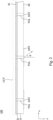
FIG. 2 is a side perspective view of the wireless communication device of the present disclosure. -
FIG. 3 is a plot of a part of a multi-branch circuit according to some embodiments of the present disclosure. -
FIG. 4 is a plot of the multi-branch circuit with an unequal Wilkinson power divider according to other embodiments of the present disclosure. -
FIG. 5 is a top perspective view of the wireless communication device according to other embodiments of the present disclosure. -
FIG. 6 is a bottom perspective view of the wireless communication device for vertical polarization according to other embodiments of the present disclosure. -
FIG. 7 is a bottom perspective view of the wireless communication device for horizontal polarization according to other embodiments of the present disclosure. -
FIG. 8 is antenna gain of the wireless communication device for the horizontal polarization according to some embodiments of the present disclosure. -
FIG. 9 is antenna gain of the wireless communication device for the vertical polarization according to some embodiments of the present disclosure. - Reference will now be made in detail to the present embodiments of the disclosure, examples of which are illustrated in the accompanying drawings. Wherever possible, the same reference numbers are used in the drawings and the description to refer to the same or like parts.
- Refer to
FIG. 1 andFIG. 2 , whereFIG. 1 is a top perspective view of a wireless communication device100 of the present disclosure, andFIG. 2 is a side perspective view of thewireless communication device 100 of the present disclosure, whereFIG. 2 is the side perspective view along a line segment from terminal point A to terminal point A in thewireless communication device 100 ofFIG. 1 . In this embodiment, thewireless communication device 100 includes a substrate S, a ground layer G, a multi-branch circuit CCT, and multiple antenna elements ANT. - Notably, although this embodiment adopts a configuration in which a quantity of the multiple antenna elements ANT is 16 and the quantity of each row of the multiple antenna elements ANT is 8, to achieve requirement that a beamwidth is 11 degrees and antenna gain of a main beam needs to be more than or equal to 15dB, the quantity of the multiple antenna elements ANT and the quantity of each row can also be adjusted according to other requirements of beamwidth and antenna gain.
- Furthermore, the substrate S includes a first surface S1 and a second surface S2 corresponding to each other. The ground layer G is disposed between the first surface S1 and the second surface S2. In some embodiments, the substrate S can be a printed circuit board (PCB) made of an insulating material, where material of the substrate S can be Teflon (PTFE) or epoxy resin (FR4) and other materials commonly used to manufacture PCBs. In some embodiments, the ground layer G can be made of a metal material such as copper foil.
- Furthermore, the multi-branch circuit CCT is disposed on the first surface S1, where the multi-branch circuit CCT includes a signal feeding terminal and multiple signal output terminals, where the multiple feeding branches are formed between the signal feeding terminal and the multiple signal output terminals. In some embodiments, the multi-branch circuit has multiple branch nodes in multiple stages to form the multiple feeding branches between the signal feeding terminal and the multiple signal output terminals.
- In some embodiments, the multiple branch nodes can be multiple unequal Wilkinson power dividers, and the multiple unequal Wilkinson power dividers are used for improving isolation between the multiple antenna elements ANT to control antenna gain of the multiple antenna elements ANT, thereby reducing sidelobe interference. In some embodiments, the multiple unequal Wilkinson power dividers are further used for controlling the antenna gain of the multiple antenna elements ANT by controlling the multiple power ratios between the multiple antenna elements ANT.
- Furthermore, the multiple antenna elements ANT are disposed on the second surface S2, where the multiple antenna elements are connected to the multiple signal output terminals through respective via holes VIA, and are configured for beamforming. In some embodiments, a feeding point FP of each antenna elements ANT can be connected to corresponding signal output terminal through the corresponding via hole VIA.
- Furthermore, a length difference between path lengths of the feeding branches of two adjacent antenna elements in a horizontal direction (i.e., +x direction) is configured for controlling a beam angle θ of the multiple antenna elements (i.e., an angle between directions of a generated beam of the multiple antenna elements ANT and a normal direction of the second surface S2). In some embodiments, the antenna element ANT can be a patch antenna or other antennas applicable to an antenna array. In other words, the multiple antenna elements ANT can form one or more antenna arrays, where the antenna arrays can be patch antenna arrays.
- In some embodiments, when each of the multiple antenna elements ANT is a vertically polarized patch antenna, the multiple antenna elements ANT are disposed on the second surface S2 in a horizontal mirror plane from row to row. In addition, when each of the multiple antenna elements ANT is a horizontally polarized patch antenna, the multiple antenna elements ANT are disposed on the second surface S2 in a vertical mirror plane from column to column.
- In some embodiments, a phase difference between two adjacent antenna elements ANT in the horizontal direction is proportional to the length difference. In some embodiments, the beam angle θ of the multiple antenna elements ANT is proportional to the length difference. In some embodiments, an antenna distance d between geometric center positions of the adjacent two of the multiple antenna elements ANT in the horizontal direction is one-half wavelength of a center frequency of a resonant frequency band of the multiple antenna elements ANT.
- With the
wireless communication device 100 of the present disclosure, the beam direction of thewireless communication device 100 can be adjusted by using the path lengths of the feeding branches in the multi-branch circuit CCT. In addition, since thewireless communication device 100 adopts a large quantity of the antenna elements, the beamwidth of the main beam can also be greatly reduced, so as to solve the inter-beam interference caused by the need to use multiple beams in a small space. - The
wireless communication device 100 is further described below with an actual example. - Refer to
FIG. 3, and FIG. 3 is a plot of a part of a multi-branch circuit CCT according to some embodiments of the present disclosure, where the part of the multi-branch circuit CCT is upper half of the multi-branch circuit CCT inFIG. 1 . As shown inFIG. 3 , the part of the multi-branch circuit CCT includes a signal feeding terminal IN and 8 signal output terminals OUT1∼OUT8, and seven branch nodes ND1 to ND7 of three stages ST1 to ST3 exist between the signal feeding terminal IN and the signal output terminals OUT1 to OUT8 to form multiple feeding branches. - Further, the first feeding branch can be formed from the signal feeding terminal IN through the branch nodes ND1, ND2 and ND4 to the signal output terminal OUT1 in sequence. A second feeding branch can be formed from the signal feeding terminal IN through the branch nodes ND1, ND2 and ND4 to the signal output terminal OUT2 in sequence. By analogy, the third to eighth feeding branches can be formed between the signal feeding terminal IN and the signal output terminals OUT3 to OUT8.
- On the other hand, for the stage ST1, the length difference between the path length of the first feeding branch and the path length of the second feeding branch is ΔL, and the length difference between the path length of the second feeding branch and the path length of the third feeding branch is also ΔL. By analogy, the length difference between the path lengths of the other two adjacent feeding branches is also ΔL. In other words, the path lengths of the first to eighth feeding branches can form an arithmetic sequence.
- For example, for the stage ST1, the length difference can be calculated from the path length from the branch node ND4 to the signal output terminal OUT1 and the path length from the branch node ND4 to the signal output terminal OUT2, where this difference in length is ΔL. In addition, the length difference can be calculated from the path length from the branch node ND5 to the signal output terminal OUT3 and the path length from the branch node ND5 to the signal output terminal OUT4, where this difference in length is also ΔL. By analogy, the length difference corresponding to the output terminal OUT5 and the output terminal OUT6 and the length difference corresponding to the output terminal OUT7 and the output terminal OUT8 are also ΔL.
- Furthermore, for the stage ST2, the path difference between the path length, which is from the signal feeding terminal IN to the branch node ND4 through the branch nodes ND1 and ND2 in sequence, and the path length, which is from the signal feeding terminal IN to the branch node ND5 through the branch nodes ND1 and ND2 in sequence, is double ΔL, and the path difference between the path length, which is from the signal feeding terminal IN to the branch node ND5 through the branch nodes ND1 and ND2 in sequence, and the path length, which is from the signal feeding terminal IN to the branch node ND6 through the branch nodes ND1 and ND3 in sequence, is also double ΔL. By analogy, in the stage ST2, the length difference between the path lengths of other adjacent paths is also double ΔL (also forming an arithmetic progression).
- For example, for the stage ST2, the length difference can be calculated from the path length from the branch node ND2 to the branch node ND4 and the path length from the branch node ND2 to the branch node ND5, where this length difference is double ΔL. In addition, the length difference can be calculated from the path length of the branch node ND3 to the branch node ND6 and the path length of the branch node ND3 to the branch node ND7, where the length difference is also double ΔL.
- Furthermore, for the stage ST3, the path difference between the path length, which is from the signal feeding terminal IN to the branch node ND2 through the branch node ND1, and the path length, which is from the signal feeding terminal IN to the branch node ND3 through the branch node ND1, is four times ΔL.
- For example, for the stage ST3, the length difference can be calculated from the path length from the branch node ND1 to the branch node ND2 and the path length from the branch node ND1 to the branch node ND3, where this length difference is four times ΔL.
- In this way, the beam angle θ of the multiple antenna elements ANT can be adjusted by using the value ΔL of the length difference corresponding to the stage ST1 according to requirements of antenna design.
- Notably, the phase of output signals of the signal output terminals OUT1 to OUT8 can form another arithmetic sequence. In addition, the phase difference between two adjacent signal output terminals is proportional to the above-mentioned length difference.
- With the above arrangement, relationship between the beam angle θ of the multiple antenna elements ANT, the antenna distance d, and the value ΔL of the length difference corresponding to the stage ST1 is shown in the following equation (1).

- It can be known from Equation (1) that when a larger beam angle θ is required, the lengths of the lines in the multi-branch circuit CCT can be adjusted to generate a larger value ΔL of the length difference. Conversely, when a smaller beam angle θ is required, the lengths of the lines in the multi-branch circuit CCT can be adjusted to produce a smaller value ΔL of the length difference. In other words, the value ΔL of the length difference (which can be any positive number) can be selected according to requirement, and the beam angle of the
wireless communication device 100 can be adjusted by using the value ΔL of the length difference, and there is no special limitation on ΔL. - Refer to
FIG. 4, and FIG. 4 is a plot of the multi-branch circuit CCT' with an unequal Wilkinson power divider according to other embodiments of the present disclosure. As shown inFig. 4 , each branch node in the multi-branch circuit CCT ofFig. 3 can adopt an unequal Wilkinson power divider to form a circuit structure of a multi-branch circuit CCT' with an unequal Wilkinson power divider, so as to improve the isolation between the two output terminals of the unequal Wilkinson power divider, thereby adjusting the power difference between the two output terminals. Notably, relationship between the path lengths in the stages ST1 to ST3 in the multi-branch circuit CCT' is the same as that of the multi-branch circuit CCT. Therefore, no further description is given here. - In order to set the power difference between the sidelobe and the main beam to be more than or equal to 18dB, the signal output terminal OUT1 in the multi-branch circuit CCT' can be used as a reference, and power of the signal output terminals OUT1 to OUT8 in the multi-branch circuit CCT' as shown in the following table (1).
Signal output terminal OUT1 OUT2 OUT3 OUT4 OUT5 OUT6 OUT7 OUT8 Power (dB) 0.34 0.44 0.77 1.00 1.00 0.77 0.44 0.34 - It can be known from Table (1) that there is a specific power ratio between the signal output terminals OUT1 to OUT8. Thereby, a power difference between the two output terminals of the unequal Wilkinson power divider in the multi-branch circuit CCT' can be adjusted according to these power ratios.
- Furthermore, based on the above Table (1), by using the unequal Wilkinson power divider, the power difference between the two output terminals of the branch node ND4 can be adjusted to 1.12 dB, the power difference between the two output terminals of the branch node ND5 can be adjusted to 1.16 dB, the power difference between the two output terminals of the branch node ND2 can be adjusted to 3.59 dB, and the power difference between the two output terminals of the branch node ND1 can be adjusted to 0 dB. By analogy, the power difference between the two output terminals of branch nodes ND7, ND6 and ND3 can be adjusted in the same way.
- With the above arrangement, the power difference between the main beam and the sidelobe of the multiple antenna elements ANT can be increased to more than 18 dB for controlling the antenna gain of the multiple antenna elements ANT to be more than 15 dB, thereby reducing sidelobe interference.
- Refer to
FIG. 5, and FIG. 5 is a top perspective view of thewireless communication device 100 according to other embodiments of the present disclosure. As shown inFIG. 5 , the multi-branch circuit CCT' (corresponding to the antenna elements ANT in the first row) in the upper half of thewireless communication device 100 inFIG. 5 is the multi-branch circuit CCT' shown inFIG. 4 , and the difference betweenFIG. 5 andFIG. 1 only lies in the branch nodes ND1 to ND7 in the multi-branch circuit CCT, so other similarities will not be repeated. - Refer to
FIG. 6, and FIG. 6 is a bottom perspective view of thewireless communication device 100 for vertical polarization according to other embodiments of the present disclosure. As shown inFIG.6 , the antenna elements ANT in rows 1 to 2 are a vertically polarized antenna array with a beam angle of -5 degrees, the antenna elements ANT in rows 3 to 4 are a vertically polarized antenna array with a beam angle of -16 degrees, the antenna elements ANT inrows 5 to 6 are a vertically polarized antenna array with a beam angle of 5 degrees, and the antenna elements ANT in rows 7 to 8 are a vertically polarized antenna array with a beam angle of 16 degrees. - In addition, with the antenna elements ANT in the first row as a reference, the antenna elements ANT in the second row can be disposed in a horizontal mirror plane from row to row. In other words, the feeding point FP of the antenna element ANT in the first row is close to an upper edge of the antenna element ANT in the first row, and the feeding point FP of the antenna unit ANT in the second row is close to a lower edge of the antenna unit ANT in the second row. By analogy, each antenna array can have the same arrangement.
- Refer to
FIG. 7, and FIG. 7 is a bottom perspective view of thewireless communication device 100 for horizontal polarization according to other embodiments of the present disclosure. As shown inFIG.7 , the antenna elements ANT in rows 1 to 2 are a horizontally polarized antenna array with a beam angle of -5 degrees, the antenna elements ANT in rows 3 to 4 are a horizontally polarized antenna array with a beam angle of -16 degrees, the antenna elements ANT inrows 5 to 6 are a horizontally polarized antenna array with a beam angle of 5 degrees, and the antenna elements ANT in rows 7 to 8 are a horizontally polarized antenna array with a beam angle of 16 degrees. - In addition, with the antenna elements ANT in the columns 1 to 4 as a reference, the antenna elements ANT in the columns 8 to 5 can be disposed in a vertical mirror plane from column to column. In other words, the feeding points FP of the antenna elements ANT in the columns 1 to 4 are respectively close to left sides of the antenna elements ANT in the columns 1 to 4, and the feeding points FP of the antenna elements ANT in the columns 8 to 5 are respectively close to right sides of the antenna elements ANT in the columns 8 to 5. By analogy, each antenna array can have the same arrangement.
- On the other hand, when the
wireless communication device 100 needs to cover 45 degrees in the horizontal direction, 8 users exist, and the antenna gain needs to be more than or equal to 15 dB, the antenna arrays of the above-mentionedFIG. 6 andFIG. 7 can be used simultaneously, and the multi-branch circuit shown inFIG. 5 is used in each antenna array. By this, 4 beams can be generated in the horizontal and the vertical polarization directions to generate 8 beams, where the beamwidth of each beam is about 11 degrees and the antenna gain of each antenna array is about 15 dB. In addition, the cross polarization between the vertical polarization and the horizontal polarization of thewireless communication device 100 can be more than 25 dB. In this way, the effects of narrow beamwidth, low sidelobe interference, low power consumption and low cost can be achieved at the same time. - Reference is made to
FIG. 8, and FIG. 8 is antenna gain of thewireless communication device 100 for the horizontal polarization according to some embodiments of the present disclosure. As shown inFIG. 8 , the curve CH1_HM1 is the antenna gain of the antenna element ANT in the rows 3 to 4 inFIG. 7 , the curve CH1_HM2 is the antenna gain of the antenna element ANT in therows 5 to 6 inFIG. 7 , The curve CH2_HM1 is the antenna gain of the antenna element ANT in the rows 1 to 2 inFig. 7 , and the curve CH2_HM2 is the antenna gain of the antenna element ANT in the rows 7 to 8 inFIG. 7 . - It can be known from
FIG. 8 , the antenna gain of each antenna array is also about 15 dB, and the beam directions of the horizontal polarization of each antenna array are also -16 degrees, -5 degrees, 5 degrees, and 16 degrees, respectively, and the power difference between the sidelobe and the main beam is also more than 18 dB. - Reference is made to
FIG. 9, and FIG. 9 antenna gain of thewireless communication device 100 for the vertical polarization according to some embodiments of the present disclosure. As shown inFIG. 9 , the curve CH1_VM1 is the antenna gain of the antenna element ANT in the rows 3 to 4 inFIG. 6 , the curve CH1_VM2 is the antenna gain of the antenna element ANT in therows 5 to 6 inFIG. 6 , the curve CH2_VM1 is the antenna gain of the antenna element ANT in the rows 1 to 2 inFIG. 6 , and the curve CH2_VM2 is the antenna gain of the antenna element ANT in the rows 7 to 8 inFIG. 6 . - It can be known from
FIG. 9 , the antenna gain of each antenna array is about 15dB, and the beam directions of the vertical polarization of each antenna array are -16 degrees, -5 degrees, 5 degrees and 16 degrees, respectively, and the power difference between the sidelobe and the main beam is more than 18 dB. - In summary, the wireless communication device of the present disclosure can utilize the length difference between the path lengths of the feeding branches of two adjacent antenna elements in the horizontal direction for controlling the beam angle of the antenna elements, and reduce the beamwidth by using a large quantity of the antenna elements. In addition, the power ratios between the branch nodes of the multi-branch circuit with multiple stages can be adjusted to control the antenna gain of the antenna elements, thereby reducing sidelobe interference. On the other hand, such the arrangement also greatly reduces power consumption and cost.
Claims (15)
- An antenna structure, characterized by comprising:a substrate (S) comprising a first surface (S1) and a second surface (S2);a ground layer (G), disposed between the first surface (S1) and the second surface (S2);a multi-branch circuit (CCT), disposed on the first surface (S1), wherein the multi-branch circuit (CCT) comprises a signal feeding terminal (IN) and a plurality of signal output terminals, wherein a plurality of feeding branches are formed between the signal feeding terminal (IN) and the plurality of signal output terminals (OUT1-OUT8); anda plurality of antenna elements (ANT), disposed on the second surface (S2), wherein the plurality of antenna elements (ANT) are connected to the plurality of signal output terminals (OUT1-OUT8) through respective via holes (VIA), and are configured for beamforming, wherein a length difference (ΔL) between path lengths of the feed branches of two adjacent antenna elements (ANT) in a horizontal direction (x) is configured for controlling a beam angle (θ) of the plurality of antenna elements (ANT).
- The antenna structure (100) of claim 1, wherein the multi-branch circuit (CCT) has a plurality of branch nodes (ND1-ND7) of a plurality of stages (ST1-ST3) to form the plurality of feeding branches between the signal feeding terminal (IN) and the plurality of signal output terminals (OUT1-OUT8).
- The antenna structure of claim 2, wherein the plurality of stages (ST1-ST3) comprise a first stage (ST1), and the first stage (ST1) is connected to the plurality of signal output terminals (OUT1-OUT8), wherein
a path length difference (ΔL) between the two adjacent signal output terminals and the branch node (ND1-ND7) in the first stage (ST1) connected to the adjacent two signal output terminals is equal to the length difference (ΔL). - The antenna structure of claim 3, wherein the plurality of stages (ST1-ST3) further comprise a second stage (ST2), and the second stage (ST2) is connected to the first stage (ST1), wherein
a path length difference (2*ΔL) between the adjacent two branch nodes of the first stage (ST1) and the branch node in the second stage (ST2) connected to the adjacent two branch nodes of the first stage (ST1) is equal to double the length difference (ΔL). - The antenna structure of claim 4, wherein the plurality of stages (ST1-ST3) further comprise a third stage (ST3), and the third stage (ST3) is connected between the second stage (ST2) and the signal feeding terminal (IN), wherein
a path length difference (4*ΔL) between the adjacent two branch nodes of the second stage (ST2) and the branch node in the third stage (ST3) connected to the adjacent two branch nodes of the second stage (ST2) is equal to four times the length difference (ΔL). - The antenna structure of claim 1, wherein the plurality of branch nodes (ND1-ND7) are a plurality of unequal Wilkinson power dividers, and the plurality of unequal Wilkinson power dividers are configured for improving isolation between the plurality of antenna elements (ANT) to control antenna gain of the plurality of antenna elements (ANT), thereby reducing sidelobe interference,
wherein the plurality of unequal Wilkinson power dividers are further configured for controlling a plurality of power ratios between the plurality of antenna elements (ANT) to control the antenna gain of the plurality of antenna elements (ANT). - The antenna structure of any of claims 1-6, wherein a phase difference between the two adjacent antenna elements (ANT) in the horizontal direction (x) is proportional to the length difference (ΔL), wherein the beam angle (θ) of the plurality of antenna elements (ANT) are proportional to the length difference (ΔL),
wherein an antenna distance between geometric center positions of the adjacent two of the plurality of antenna elements (ANT) in the horizontal direction (x) is one-half wavelength of a center frequency of a resonant frequency band of the plurality of antenna elements (ANT). - The antenna structure (100) of any of claims 1-6, whereinwhen each of the plurality of antenna elements (ANT) is a vertically polarized patch antenna, the plurality of antenna elements (ANT) are disposed on the second surface (S2) in a horizontal mirror plane from row to row, andwhen each of the plurality of antenna elements (ANT) is a horizontally polarized patch antenna, the plurality of antenna elements (ANT) are disposed on the second surface (S2) in a vertical mirror plane from column to column.
- A wireless communication device (100), characterized by comprising:
a plurality of antenna arrays, wherein each of the plurality of antenna arrays comprises:a substrate (S) comprising a first surface (S1) and a second surface (S2);a ground layer (G), disposed between the first surface (S1) and the second surface (S2);a multi-branch circuit (CCT), disposed on the first surface (S1), wherein the multi-branch circuit (CCT) comprises a signal feeding terminal (IN) and a plurality of signal output terminals (OUT1-OUT8), wherein a plurality of feeding branches are formed between the signal feeding terminal (IN) and the plurality of signal output terminals (OUT1-OUT8); anda plurality of antenna elements (ANT), disposed on the second surface (S2), wherein the antenna elements (ANT) are connected to the plurality of signal output terminals (OUT1-OUT8) through respective via holes (VIA), and are configured for beamforming, wherein a length difference (ΔL) between path lengths of the feed branches of two adjacent antenna elements (ANT) in a horizontal direction (x) is configured for controlling a beam angle (θ) of the plurality of antenna elements (ANT). - The wireless communication device (100) of claim 9, wherein, for the each of the plurality of antenna arrays, the multi-branch circuit (CCT) has a plurality of branch nodes (ND1-ND7) of a plurality of stages (ST1-ST3) to form the plurality of feeding branches between the signal feeding terminal (IN) and the plurality of signal output terminals (OUT1-OUT8).
- The wireless communication device (100) of claim 10, wherein, for the each of the plurality of antenna arrays, the plurality of stages (ST1-ST3) comprise a first stage (ST1), and the first stage (ST1) is connected to the plurality of signal output terminals (OUT1-OUT8), wherein
for the each of the plurality of antenna arrays, a path length difference (ΔL) between the two adjacent signal output terminals and the branch node in the first stage (ST1) connected to the adjacent two signal output terminals is equal to the length difference (ΔL). - The wireless communication device (100) of claim 11, wherein, for the each of the plurality of antenna arrays, the plurality of stages (ST1-ST3) further comprise a second stage (ST2), and the second stage (ST2) is connected to the first stage (ST1), wherein
for the each of the plurality of antenna arrays, a path length difference (2*ΔL) between the adjacent two branch nodes of the first stage (ST1) and the branch node in the second stage (ST2) connected to the adjacent two branch nodes of the first stage (ST1) is equal to double the length difference (ΔL). - The wireless communication device (100) of claim 12, wherein, for the each of the plurality of antenna arrays, the plurality of stages (ST1-ST3) further comprise a third stage (ST3), and the third stage (ST3) is connected between the second stage (ST2) and the signal feeding terminal (IN), wherein
for the each of the plurality of antenna arrays, a path length difference (4*ΔL) between the adjacent two branch nodes of the second stage (ST2) and the branch node in the third stage (ST3) connected to the adjacent two branch nodes of the second stage (ST2) is equal to four times the length difference (ΔL). - The wireless communication device (100) of claim 9, wherein, for the each of the plurality of antenna arrays, the plurality of branch nodes (ND1-ND7) are a plurality of unequal Wilkinson power dividers, and the plurality of unequal Wilkinson power dividers are configured for improving isolation between the plurality of antenna elements (ANT) to control antenna gain of the plurality of antenna elements (ANT), thereby reducing sidelobe interference,
wherein, for the each of the plurality of antenna arrays, the plurality of unequal Wilkinson power dividers are further configured for controlling a plurality of power ratios between the plurality of antenna elements (ANT) to control the antenna gain of the plurality of antenna elements (ANT). - The wireless communication device (100) of any of claims 9-14, wherein, for the each of the plurality of antenna arrays, a phase difference between the two adjacent antenna elements (ANT) in the horizontal direction (x) is proportional to the length difference (ΔL), whereinwhen the each of the plurality of antenna arrays is a vertically polarized patch antenna array, for the each of the plurality of antenna arrays, the plurality of antenna elements (ANT) are disposed on the second surface (S2) in horizontal mirror plane from row to row, andwhen the each of the plurality of antenna arrays is a horizontally polarized patch antenna array, for each of the plurality of antenna arrays, the plurality of antenna elements (ANT) are disposed on the second surface (S2) in vertical mirror plane from column to column.
Applications Claiming Priority (1)
| Application Number | Priority Date | Filing Date | Title |
|---|---|---|---|
| CN202210498484.1A CN117080736A (en) | 2022-05-09 | 2022-05-09 | Antenna structures and wireless communication devices |
Publications (1)
| Publication Number | Publication Date |
|---|---|
| EP4277036A1 true EP4277036A1 (en) | 2023-11-15 |
Family
ID=84329515
Family Applications (1)
| Application Number | Title | Priority Date | Filing Date |
|---|---|---|---|
| EP22205756.4A Pending EP4277036A1 (en) | 2022-05-09 | 2022-11-07 | Antenna structure and wireless communication device |
Country Status (4)
| Country | Link |
|---|---|
| US (1) | US12512587B2 (en) |
| EP (1) | EP4277036A1 (en) |
| JP (1) | JP7645297B2 (en) |
| CN (1) | CN117080736A (en) |
Families Citing this family (2)
| Publication number | Priority date | Publication date | Assignee | Title |
|---|---|---|---|---|
| CN113381174B (en) * | 2020-02-25 | 2024-06-18 | 华为技术有限公司 | Antenna and radar |
| CN120064800A (en) * | 2023-11-29 | 2025-05-30 | 深圳富泰宏精密工业有限公司 | Test antenna device and antenna test system |
Citations (5)
| Publication number | Priority date | Publication date | Assignee | Title |
|---|---|---|---|---|
| US4973972A (en) * | 1989-09-07 | 1990-11-27 | The United States Of America As Represented By The Administrator Of The National Aeronautics And Space Adminstration | Stripline feed for a microstrip array of patch elements with teardrop shaped probes |
| US10074910B1 (en) * | 2014-08-01 | 2018-09-11 | Rockwell Collins, Inc. | Switchable X band communication panel |
| CN111370862A (en) * | 2020-03-26 | 2020-07-03 | 东南大学 | Single-port broadband dual-circular polarization dual-directional beam microstrip array antenna |
| US20200227835A1 (en) * | 2018-10-05 | 2020-07-16 | Dongwoo Fine-Chem Co., Ltd. | Antenna structure and display device including the same |
| CN112201952A (en) * | 2020-10-22 | 2021-01-08 | 上海无线电设备研究所 | Broadband large-inclination-angle low-sidelobe microstrip array antenna |
Family Cites Families (50)
| Publication number | Priority date | Publication date | Assignee | Title |
|---|---|---|---|---|
| JP2689453B2 (en) * | 1988-01-11 | 1997-12-10 | 日本電気株式会社 | Antenna device |
| JPH02164107A (en) | 1988-12-19 | 1990-06-25 | Sanyo Electric Co Ltd | Microstrip antenna |
| GB9027776D0 (en) * | 1990-12-21 | 1991-06-12 | Marconi Gec Ltd | Patch antenna |
| JPH06326510A (en) * | 1992-11-18 | 1994-11-25 | Toshiba Corp | Beam scanning antenna and array antenna |
| JPH0897620A (en) | 1994-09-22 | 1996-04-12 | Honda Motor Co Ltd | Multi-beam planar array antenna |
| GB9424119D0 (en) * | 1994-11-28 | 1995-01-18 | Northern Telecom Ltd | An antenna dow-tilt arrangement |
| JPH10303612A (en) | 1997-04-25 | 1998-11-13 | Kyocera Corp | Patch antenna |
| JPH11266118A (en) | 1998-03-17 | 1999-09-28 | Matsushita Electric Ind Co Ltd | Patch array antenna |
| WO2001059473A2 (en) * | 2000-02-08 | 2001-08-16 | Cambridge Consultants Limited | Methods and apparatus for obtaining positional information |
| US6417806B1 (en) | 2001-01-31 | 2002-07-09 | Tantivy Communications, Inc. | Monopole antenna for array applications |
| US6888504B2 (en) | 2002-02-01 | 2005-05-03 | Ipr Licensing, Inc. | Aperiodic array antenna |
| JP2004023228A (en) * | 2002-06-13 | 2004-01-22 | Matsushita Electric Ind Co Ltd | Antenna control device and phased array antenna |
| US20040100402A1 (en) * | 2002-11-26 | 2004-05-27 | Mccandless Jay | Broadband CSC2 antenna pattern beam forming networks |
| JP3988653B2 (en) * | 2003-02-10 | 2007-10-10 | 株式会社デンソー | Antenna arrangement method and radar apparatus |
| US7952534B2 (en) * | 2004-03-31 | 2011-05-31 | Toto Ltd. | Microstrip antenna |
| JP4486035B2 (en) * | 2005-12-12 | 2010-06-23 | パナソニック株式会社 | Antenna device |
| KR101490795B1 (en) * | 2008-04-25 | 2015-02-09 | 삼성전자주식회사 | Beamformer and beam forming method |
| TWI423524B (en) | 2009-05-20 | 2014-01-11 | Ind Tech Res Inst | Antenna structure with reconfigurable pattern and manufacturing method thereof |
| US20120086601A1 (en) * | 2010-10-08 | 2012-04-12 | Toyota Motor Engineering & Manufacturing North America, Inc. | Microwave antenna system |
| KR101930576B1 (en) | 2011-09-06 | 2018-12-18 | 인텔 코포레이션 | Multiband active-passive base station antenna |
| US8903454B2 (en) | 2011-11-07 | 2014-12-02 | Alcatel Lucent | Base station and radio unit for creating overlaid sectors with carrier aggregation |
| TW201401655A (en) * | 2012-06-27 | 2014-01-01 | Beam Networks Ltd | Circularly and linearly polarized planar phased array antennae and network systems employing such |
| US9395727B1 (en) * | 2013-03-22 | 2016-07-19 | Google Inc. | Single layer shared aperture beam forming network |
| US10062972B1 (en) * | 2013-04-23 | 2018-08-28 | National Technology & Engineering Solutions Of Sandia, Llc | Antenna array with low Rx and Tx sidelobe levels |
| CN103825664B (en) | 2014-02-21 | 2016-05-18 | 电信科学技术研究院 | Channel state information measuring method and device, and signal transmission method and device |
| US9735475B2 (en) * | 2014-12-01 | 2017-08-15 | Anderson Contract Engineering, Inc. | Low cost antenna array and methods of manufacture |
| US20180241135A1 (en) * | 2017-02-23 | 2018-08-23 | Taoglas Group Holdings Limited | 27-28.5 GHz Ka BAND PHASED ARRAY FAN BEAM ANTENNAS AND METHODS |
| US10153739B2 (en) | 2017-03-21 | 2018-12-11 | Panasonic Corporation | Power amplification division circuit and multi-stage type power amplification division circuit |
| JP6756300B2 (en) * | 2017-04-24 | 2020-09-16 | 株式会社村田製作所 | Array antenna |
| US11035930B2 (en) | 2017-07-26 | 2021-06-15 | Rohde & Schwarz Gmbh & Co. Kg | Antenna measurement system as well as method for controlling a measurement antenna array |
| US11177566B2 (en) | 2018-02-15 | 2021-11-16 | Apple Inc. | Electronic devices having shielded antenna arrays |
| TW201946382A (en) * | 2018-02-15 | 2019-12-01 | 美商太空探索科技公司 | Hierarchical network signal routing apparatus and method |
| US11404794B2 (en) * | 2018-06-26 | 2022-08-02 | Metawave Corporation | Multi-layer, multi-steering antenna array for millimeter wave applications |
| CN112997422B (en) * | 2018-10-31 | 2023-04-04 | 株式会社村田制作所 | Radio wave repeater and communication system |
| WO2020153283A1 (en) * | 2019-01-22 | 2020-07-30 | 株式会社村田製作所 | Antenna module and communication device |
| JP7283678B2 (en) * | 2019-03-18 | 2023-05-30 | 国立研究開発法人宇宙航空研究開発機構 | antenna device |
| US11671846B2 (en) | 2019-06-07 | 2023-06-06 | Qualcomm Incorporated | Adjacent beam determination |
| TWI706598B (en) | 2019-08-22 | 2020-10-01 | 中華電信股份有限公司 | Antenna apparatus |
| EP4429025A3 (en) | 2020-03-24 | 2024-11-20 | Outdoor Wireless Networks LLC | Radiating elements having angled feed stalks and base station antennas including same |
| EP3966898A4 (en) | 2020-03-24 | 2023-01-25 | CommScope Technologies LLC | ACTIVE ANTENNA MODULE BASE STATION ANTENNAS AND RELATED DEVICES AND METHODS |
| WO2021209151A1 (en) * | 2020-04-17 | 2021-10-21 | Telefonaktiebolaget Lm Ericsson (Publ) | Transmitter arrangement, transceiver, radio communication system and method |
| CN111725630A (en) | 2020-06-23 | 2020-09-29 | Oppo广东移动通信有限公司 | Array antenna components, antenna modules and electronic equipment |
| CN113013567A (en) | 2021-01-29 | 2021-06-22 | 中国电子科技集团公司第三十八研究所 | Chip-packaging-antenna integrated structure based on SIW multi-feed network |
| US12374789B2 (en) * | 2021-03-11 | 2025-07-29 | Telefonaktiebolaget Lm Ericsson (Publ) | Active antenna system comprising coupling paths between feed networks |
| US11539146B2 (en) * | 2021-03-19 | 2022-12-27 | United States Of America As Represented By The Secretary Of The Navy | Circular polarized phased array with wideband axial ratio bandwidth using sequential rotation and dynamic phase recovery |
| CN113270730B (en) | 2021-05-14 | 2025-07-08 | 苏州大学 | Circularly polarized array antenna with sequential rotary feed |
| TWI765755B (en) * | 2021-06-25 | 2022-05-21 | 啟碁科技股份有限公司 | Antenna module and wireless transceiver device |
| WO2023137690A1 (en) * | 2022-01-21 | 2023-07-27 | 京东方科技集团股份有限公司 | Antenna and antenna system |
| US12494835B2 (en) * | 2022-05-09 | 2025-12-09 | Delta Electronics, Inc. | Communication system |
| CN119153962B (en) * | 2024-11-11 | 2025-02-25 | 温尊伟 | A design method for beam pointing control antenna |
-
2022
- 2022-05-09 CN CN202210498484.1A patent/CN117080736A/en active Pending
- 2022-09-06 US US17/929,751 patent/US12512587B2/en active Active
- 2022-11-07 EP EP22205756.4A patent/EP4277036A1/en active Pending
-
2023
- 2023-02-07 JP JP2023017131A patent/JP7645297B2/en active Active
Patent Citations (5)
| Publication number | Priority date | Publication date | Assignee | Title |
|---|---|---|---|---|
| US4973972A (en) * | 1989-09-07 | 1990-11-27 | The United States Of America As Represented By The Administrator Of The National Aeronautics And Space Adminstration | Stripline feed for a microstrip array of patch elements with teardrop shaped probes |
| US10074910B1 (en) * | 2014-08-01 | 2018-09-11 | Rockwell Collins, Inc. | Switchable X band communication panel |
| US20200227835A1 (en) * | 2018-10-05 | 2020-07-16 | Dongwoo Fine-Chem Co., Ltd. | Antenna structure and display device including the same |
| CN111370862A (en) * | 2020-03-26 | 2020-07-03 | 东南大学 | Single-port broadband dual-circular polarization dual-directional beam microstrip array antenna |
| CN112201952A (en) * | 2020-10-22 | 2021-01-08 | 上海无线电设备研究所 | Broadband large-inclination-angle low-sidelobe microstrip array antenna |
Non-Patent Citations (1)
| Title |
|---|
| VARUM TIAGO ET AL: "Nonuniform Broadband Circularly Polarized Antenna Array for Vehicular Communications", IEEE TRANSACTIONS ON VEHICULAR TECHNOLOGY, IEEE, USA, vol. 65, no. 9, 1 September 2016 (2016-09-01), pages 7219 - 7227, XP011623092, ISSN: 0018-9545, [retrieved on 20160915], DOI: 10.1109/TVT.2015.2500520 * |
Also Published As
| Publication number | Publication date |
|---|---|
| US20230361462A1 (en) | 2023-11-09 |
| JP2023166326A (en) | 2023-11-21 |
| CN117080736A (en) | 2023-11-17 |
| US12512587B2 (en) | 2025-12-30 |
| JP7645297B2 (en) | 2025-03-13 |
Similar Documents
| Publication | Publication Date | Title |
|---|---|---|
| US11177572B2 (en) | Broadband stacked patch radiating elements and related phased array antennas | |
| US6232920B1 (en) | Array antenna having multiple independently steered beams | |
| US12244071B2 (en) | High performance folded dipole for multiband antennas | |
| US4916457A (en) | Printed-circuit crossed-slot antenna | |
| US11264732B2 (en) | Antenna module and communication apparatus | |
| DE112019000828T5 (en) | Antenna modules for phased array antennas Cross reference to related applications | |
| CN112332111B (en) | Double circular polarization expandable active subarray | |
| WO2020241271A1 (en) | Sub-array antenna, array antenna, antenna module, and communication device | |
| US11469524B2 (en) | Polarized wave shared array antenna and method for manufacturing the same | |
| US20130181880A1 (en) | Low profile wideband multibeam integrated dual polarization antenna array with compensated mutual coupling | |
| US11916298B2 (en) | Patch antenna | |
| CN108417971B (en) | Dual polarized antenna array and dual polarized phased array antenna | |
| US12494835B2 (en) | Communication system | |
| US11355867B2 (en) | Polarized wave shared array antenna and method for manufacturing the same | |
| US12512587B2 (en) | Antenna structure and wireless communication device | |
| US20240305018A1 (en) | Phased array antenna | |
| US20220094065A1 (en) | Low loss wideband radiator for base station antenna | |
| TWI835133B (en) | Antenna structure and wireless communication device | |
| US20240072439A1 (en) | Antenna device | |
| RU233205U1 (en) | Broadband beamforming device | |
| US20260031530A1 (en) | Array antenna for reducing grating lobe and cross polarization leakage | |
| RU2796807C2 (en) | Antenna array with independently rotating radiant elements | |
| RU2820493C1 (en) | PHASED ANTENNA ARRAY FOR SATELLITE COMMUNICATION IN Ku-BAND | |
| RU2843831C1 (en) | Three-dimensional element of phased antenna array with operating frequency range in microwave region | |
| JP2002223120A (en) | Circularly polarized planar array antenna |
Legal Events
| Date | Code | Title | Description |
|---|---|---|---|
| PUAI | Public reference made under article 153(3) epc to a published international application that has entered the european phase |
Free format text: ORIGINAL CODE: 0009012 |
|
| STAA | Information on the status of an ep patent application or granted ep patent |
Free format text: STATUS: REQUEST FOR EXAMINATION WAS MADE |
|
| 17P | Request for examination filed |
Effective date: 20230824 |
|
| AK | Designated contracting states |
Kind code of ref document: A1 Designated state(s): AL AT BE BG CH CY CZ DE DK EE ES FI FR GB GR HR HU IE IS IT LI LT LU LV MC ME MK MT NL NO PL PT RO RS SE SI SK SM TR |
|
| STAA | Information on the status of an ep patent application or granted ep patent |
Free format text: STATUS: EXAMINATION IS IN PROGRESS |
|
| 17Q | First examination report despatched |
Effective date: 20250219 |