EP4277019A1 - Waveguide assembly - Google Patents
Waveguide assembly Download PDFInfo
- Publication number
- EP4277019A1 EP4277019A1 EP22172920.5A EP22172920A EP4277019A1 EP 4277019 A1 EP4277019 A1 EP 4277019A1 EP 22172920 A EP22172920 A EP 22172920A EP 4277019 A1 EP4277019 A1 EP 4277019A1
- Authority
- EP
- European Patent Office
- Prior art keywords
- waveguide
- plate
- pins
- emitter
- waveguide assembly
- Prior art date
- Legal status (The legal status is an assumption and is not a legal conclusion. Google has not performed a legal analysis and makes no representation as to the accuracy of the status listed.)
- Granted
Links
Images

Classifications
-
- H—ELECTRICITY
- H01—ELECTRIC ELEMENTS
- H01P—WAVEGUIDES; RESONATORS, LINES, OR OTHER DEVICES OF THE WAVEGUIDE TYPE
- H01P5/00—Coupling devices of the waveguide type
- H01P5/08—Coupling devices of the waveguide type for linking dissimilar lines or devices
- H01P5/10—Coupling devices of the waveguide type for linking dissimilar lines or devices for coupling balanced lines or devices with unbalanced lines or devices
- H01P5/107—Hollow-waveguide/strip-line transitions
-
- H—ELECTRICITY
- H01—ELECTRIC ELEMENTS
- H01P—WAVEGUIDES; RESONATORS, LINES, OR OTHER DEVICES OF THE WAVEGUIDE TYPE
- H01P1/00—Auxiliary devices
- H01P1/20—Frequency-selective devices, e.g. filters
- H01P1/2005—Electromagnetic photonic bandgaps [EPB], or photonic bandgaps [PBG]
Definitions
- the invention relates to a waveguide assembly with a waveguide and an emitter of electromagnetic waves.
- the waveguide may be used in a radar sensor, for example in a vehicle.
- Waveguides are well known in the art for guiding electromagnetic waves, e.g. in the radiofrequency range, in a variety of apparatuses.
- the electromagnetic waves are often supplied to the waveguide from an emitter of electromagnetic waves coupled to a suitable electric circuit, which typically is located on a printed circuit board (PCB); an example of such waveguides can be found in US 2021 / 0 028 527 A1 .
- the PCB in prior art is also used to close the waveguide on one side, which implies constraints for the PCB, as it has to correspond in size and shape to the waveguide.
- a PCB has two opposite sides on which electronic components can be placed in principle, if the PCB is used to close the waveguide, placing electronic components on the side of the PCB towards the waveguide could interfere with the propagation of electromagnetic waves in the waveguide.
- Claim 8 relates to a corresponding radar sensor and claim 9 to a corresponding vehicle.
- the waveguide assembly includes a main waveguide comprising an arrangement of electrically conductive pins protruding from a basis and a circuit with an emitter for electromagnetic waves.
- the basis is of an electrically conductive material and may in particular be plate-shaped.
- the electrically conductive pins may be integral with the basis.
- a plate which is different from the basis and which comprises an electrically conductive material is positioned between the main waveguide and the emitter. The plate has an opening for electromagnetic waves from the emitter to pass through the plate. Furthermore, on a side of the plate opposite the main waveguide a group of electrically conductive pins is provided.
- the group of pins surrounds the emitter and the opening such that the group of pins forms a first transition waveguide for passing electromagnetic radiation from the emitter through the opening.
- the pins of the group of pins may for example be positioned such that their positions in a plane parallel to the plate trace out an open or closed polygon.
- the plate closes the waveguide at least on one side, a function which in prior art was achieved by a PCB including the emitter.
- a PCB including the emitter As the functions of closing the waveguide and carrying circuits, including the emitter, for addressing the waveguide, are now split between the plate and a separate component, like a PCB, this separate component is not subject to constraints imposed by the shape of the waveguide. Likewise, the waveguide is not constrained in shape by requirements of the prior art PCB. It is furthermore possible to independently choose suitable materials for plate and PCB or other circuit component. If a PCB is used for the circuits and emitter, as the PCB does not now close the waveguide, electronic components can be placed on opposite sides of the PCB, not just on one side of the PCB which is not towards the waveguide.
- the electromagnetic waves the emitter is configured to emit may for example be in the radiofrequency range or in the range of millimetre waves.
- the conductive material of the plate is a metal or a metallised plastic, i.e. a plastic substrate fully covered with a metal layer.
- the plate may also consist entirely of metal.
- the pins of the group of pins surrounding the emitter i.e. the pins forming the first transition waveguide between the emitter and the plate, extend through the plate.
- these pins can function as additional pins of the main waveguide.
- these pins can form part of a second transition waveguide located between the plate and the main waveguide.
- a second transition waveguide is located between the plate and the main waveguide even if the pins of the first transition waveguide do not extend through the plate. Either way, if there is a second transition waveguide, electromagnetic waves from the emitter, guided by the first transition waveguide, are passed through the opening in the plate into the second transition waveguide, and from there the electromagnetic waves are passed on into the main waveguide.
- the waveguide assembly includes an electrically conductive block, for example a metal block, attached to the pins of the group of pins surrounding the emitter. This stabilises these pins mechanically.
- the conductive block is positioned in a cut-out of the plate and extends to the side of the plate where there is the main waveguide.
- the plate is connected to the conductive block via a structure including at least one step.
- a structure including at least one step This allows a more reliable bonding between the plate and the conductive block by, for instance, gluing, soldering, or welding and serves to define the position of the plate relative to the block in a more stable fashion. Also, such a structure reduces electromagnetic leakage from the waveguide assembly.
- a radar sensor according to the invention has a waveguide assembly according to the invention, as described above.
- Such a radar sensor is less constrained in its manufacture, due to the reduced constraints on the manufacture of the waveguide assembly. This provides more freedom, for example for more efficient design.
- a vehicle according to the invention has a radar sensor according to the invention, as just described.
- the advantages in manufacture of the radar sensor carry over to the manufacture of the vehicle.
- a more efficient radar sensor operates more efficiently in the vehicle and therefore contributes to safety.
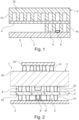
- Fig. 1 shows an embodiment of the waveguide assembly 1 according to the invention.
- a main waveguide 3 with pins 31 protruding from a basis 32 is closed by an electrically conductive plate 4 on a side opposite to the basis 32.
- a printed circuit board (PCB) 2 carries an emitter 6 for electromagnetic waves and has circuitry (not shown) for controlling the emitter 6.
- a first transition waveguide 5 is provided for passing electromagnetic waves from the emitter 6 through an opening (not shown) in the plate 4 into the main waveguide 3.
- the transition waveguide 5 has pins 51 which surround the emitter 6 at least partially.
- the pins 51 may extend through the plate 4 and on the side of the plate 4 opposite the PCB 2 function as additional pins of the main waveguide 3.
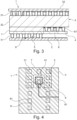
- Fig. 2 shows an embodiment of the waveguide assembly 1 according to the invention.
- the view here is a front view, i.e. electromagnetic waves in the main waveguide 3 travel in a direction orthogonal to the plane of the drawing.
- the main waveguide 3 has a basis 32 with pins 31.
- On the side of basis 32 opposite pins 31 a second transition waveguide 8 with pins 81 is provided.
- Conductive plate 4 closes main waveguide 3 and second transition waveguide 8 on one side towards PCB 2.
- a first transition waveguide 5 with pins 51 is provided between PCB 2 and plate 4.
- PCB 2 carries an emitter 6 for electromagnetic waves, for example implemented as a microstrip patch.
- a cover 33 closes the main waveguide 3 at the side of the pins 31.
- a conductive block 7 is provided between the basis 32 of the main waveguide 3 and the plate 4, to stabilise pins 51 of the first transition waveguide 5. The pins 51 are attached to block 7.
- Block 7 extends into a cut-out 42 in the plate 4.
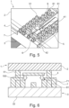
- Fig. 3 shows the waveguide assembly 1 shown in Fig. 2 in a side view.
- the direction of propagation of electromagnetic waves in the main waveguide 3 is parallel to the plane of the drawing. All elements shown have already been discussed in the context of Fig. 2 .
- the second transition waveguide 8 with pins 81 extends longer along the main waveguide 3 than the first transition waveguide 5 with pins 51.
- Fig. 2 it is also shown how the pins 51 of the first transition waveguide 5 surround the emitter 6 for electromagnetic waves.
- Fig. 4 shows a portion of a waveguide assembly 1 according to the invention, seen from the side of the emitter 6 for electromagnetic waves.
- Emitter 6 is supplied with energy via supply line 61.
- Pins 51 of the first transition waveguide 5 here surround emitter 6 on three sides, the positions of the pins 51 tracing out a rectangle open on one side, corresponding to a "U"-shape.
- Pins 51 are attached to a conductive block 7, stabilising the pins 51 mechanically.
- second transition waveguide 8 On the other side of conductive plate 4, from the perspective of the drawing behind plate 4, is second transition waveguide 8 with pins 81, part of which is also visible through opening 41 in plate 4.
- Fig. 5 shows a portion of a waveguide assembly 1 according to the invention, seen from the side of the emitter 6 for electromagnetic waves.
- Emitter 6 is supplied with energy via supply line 61.
- Most of the structure shown is covered by the PCB 2.
- Pins 51 of first transition waveguide 5 surround emitter 6 in a "U"-shape fashion as in the case of Fig. 4 .
- Conductive block 7 is partially inserted in a corresponding cut-out 42 of plate 4. Also indicated is part of the main waveguide 3.
- Fig. 6 shows a portion of a waveguide assembly 1 according to the invention. Shown are pins 51 of the first transition waveguide, and conductive block 7 mechanically stabilising these pins 51. Further shown are pins 81 of the second transition waveguide and basis 32 of main waveguide 3. Also shown is plate 4, however not in its mounted position. Arrows 100 indicate how plate 4 is to be set into recesses or steps 71 provided in conductive block 7 for increased robustness and mechanical stability of the assembly.
- Figs. 7 to 9 show various possibilities of connecting the plate 4 to the conductive block 7.
- the connection has to be electrically conductive and can for example be realised by welding, soldering or gluing.
- Fig. 7 shows a simple butt joint.
- Fig. 8 shows a profiled connection, more precisely a single step 71.
- Fig. 9 shows a profiled connection, more precisely a double step 72.
- Single step and double step provide additional stability due to their shape and increase the contact surface between plate 4 and block 7 available for, e.g., soldering, welding, or gluing.
- a profiled connection contributes to reducing electromagnetic leakage through the connection.
- Fig. 10 shows a vehicle 500, which according to the invention has a radar sensor 400 according to the invention.
- the radar sensor 400 according to the invention has a waveguide assembly 1 according to the invention.
Landscapes
- Physics & Mathematics (AREA)
- Electromagnetism (AREA)
- Optics & Photonics (AREA)
- Radar Systems Or Details Thereof (AREA)
Abstract
Description
- The invention relates to a waveguide assembly with a waveguide and an emitter of electromagnetic waves. The waveguide may be used in a radar sensor, for example in a vehicle.
- Waveguides are well known in the art for guiding electromagnetic waves, e.g. in the radiofrequency range, in a variety of apparatuses. The electromagnetic waves are often supplied to the waveguide from an emitter of electromagnetic waves coupled to a suitable electric circuit, which typically is located on a printed circuit board (PCB); an example of such waveguides can be found in
US 2021 / 0 028 527 A1 . The PCB in prior art is also used to close the waveguide on one side, which implies constraints for the PCB, as it has to correspond in size and shape to the waveguide. Furthermore, while a PCB has two opposite sides on which electronic components can be placed in principle, if the PCB is used to close the waveguide, placing electronic components on the side of the PCB towards the waveguide could interfere with the propagation of electromagnetic waves in the waveguide. - It therefore is an object of the invention to provide a waveguide assembly overcoming the above constraints.
- This object is achieved by a waveguide assembly according to
claim 1.Claim 8 relates to a corresponding radar sensor and claim 9 to a corresponding vehicle. - The waveguide assembly according to the invention includes a main waveguide comprising an arrangement of electrically conductive pins protruding from a basis and a circuit with an emitter for electromagnetic waves. The basis is of an electrically conductive material and may in particular be plate-shaped. The electrically conductive pins may be integral with the basis. According to the invention, a plate which is different from the basis and which comprises an electrically conductive material is positioned between the main waveguide and the emitter. The plate has an opening for electromagnetic waves from the emitter to pass through the plate. Furthermore, on a side of the plate opposite the main waveguide a group of electrically conductive pins is provided. The group of pins surrounds the emitter and the opening such that the group of pins forms a first transition waveguide for passing electromagnetic radiation from the emitter through the opening. The pins of the group of pins may for example be positioned such that their positions in a plane parallel to the plate trace out an open or closed polygon.
- The plate closes the waveguide at least on one side, a function which in prior art was achieved by a PCB including the emitter. As the functions of closing the waveguide and carrying circuits, including the emitter, for addressing the waveguide, are now split between the plate and a separate component, like a PCB, this separate component is not subject to constraints imposed by the shape of the waveguide. Likewise, the waveguide is not constrained in shape by requirements of the prior art PCB. It is furthermore possible to independently choose suitable materials for plate and PCB or other circuit component. If a PCB is used for the circuits and emitter, as the PCB does not now close the waveguide, electronic components can be placed on opposite sides of the PCB, not just on one side of the PCB which is not towards the waveguide. The electromagnetic waves the emitter is configured to emit may for example be in the radiofrequency range or in the range of millimetre waves.
- In an embodiment the conductive material of the plate is a metal or a metallised plastic, i.e. a plastic substrate fully covered with a metal layer. The plate may also consist entirely of metal.
- In an embodiment the pins of the group of pins surrounding the emitter, i.e. the pins forming the first transition waveguide between the emitter and the plate, extend through the plate. On the side of the plate opposite the emitter, these pins can function as additional pins of the main waveguide. Alternatively, these pins can form part of a second transition waveguide located between the plate and the main waveguide. In yet another embodiment, a second transition waveguide is located between the plate and the main waveguide even if the pins of the first transition waveguide do not extend through the plate. Either way, if there is a second transition waveguide, electromagnetic waves from the emitter, guided by the first transition waveguide, are passed through the opening in the plate into the second transition waveguide, and from there the electromagnetic waves are passed on into the main waveguide.
- In an embodiment the waveguide assembly includes an electrically conductive block, for example a metal block, attached to the pins of the group of pins surrounding the emitter. This stabilises these pins mechanically. In a specific embodiment, the conductive block is positioned in a cut-out of the plate and extends to the side of the plate where there is the main waveguide.
- In an embodiment the plate is connected to the conductive block via a structure including at least one step. This allows a more reliable bonding between the plate and the conductive block by, for instance, gluing, soldering, or welding and serves to define the position of the plate relative to the block in a more stable fashion. Also, such a structure reduces electromagnetic leakage from the waveguide assembly.
- A radar sensor according to the invention has a waveguide assembly according to the invention, as described above. Such a radar sensor is less constrained in its manufacture, due to the reduced constraints on the manufacture of the waveguide assembly. This provides more freedom, for example for more efficient design.
- A vehicle according to the invention has a radar sensor according to the invention, as just described. The advantages in manufacture of the radar sensor carry over to the manufacture of the vehicle. A more efficient radar sensor operates more efficiently in the vehicle and therefore contributes to safety.
- Below the invention and its advantages will be described in more detail with reference to the accompanying schematic drawings.
- Figure 1
- shows an embodiment of a waveguide assembly according to the invention.
- Figure 2
- shows a further embodiment of a waveguide assembly according to the invention in a front view.
- Figure 3
- shows the embodiment of
Fig. 2 in a side view. - Figure 4
- shows a portion of a waveguide assembly according to the invention.
- Figure 5
- shows a portion of a waveguide assembly according to the invention.
- Figure 6
- shows a portion of a waveguide assembly according to the invention.
- Figures 7 - 9
- show the connection between plate and conductive block.
- Figure 10
- shows a vehicle with a radar sensor according to the invention.
- The figures only show examples of how the invention can be implemented. In particular, the figures and the accompanying description are not to be taken as a limitation of the invention to the examples shown.
-
Fig. 1 shows an embodiment of thewaveguide assembly 1 according to the invention. Amain waveguide 3 withpins 31 protruding from abasis 32 is closed by an electricallyconductive plate 4 on a side opposite to thebasis 32. A printed circuit board (PCB) 2 carries anemitter 6 for electromagnetic waves and has circuitry (not shown) for controlling theemitter 6. Between theplate 4 and the PCB 2 afirst transition waveguide 5 is provided for passing electromagnetic waves from theemitter 6 through an opening (not shown) in theplate 4 into themain waveguide 3. Thetransition waveguide 5 haspins 51 which surround theemitter 6 at least partially. In certain embodiments thepins 51 may extend through theplate 4 and on the side of theplate 4 opposite thePCB 2 function as additional pins of themain waveguide 3. -
Fig. 2 shows an embodiment of thewaveguide assembly 1 according to the invention. The view here is a front view, i.e. electromagnetic waves in themain waveguide 3 travel in a direction orthogonal to the plane of the drawing. Themain waveguide 3 has abasis 32 withpins 31. On the side ofbasis 32 opposite pins 31 asecond transition waveguide 8 withpins 81 is provided.Conductive plate 4 closesmain waveguide 3 andsecond transition waveguide 8 on one side towardsPCB 2. Afirst transition waveguide 5 withpins 51 is provided betweenPCB 2 andplate 4.PCB 2 carries anemitter 6 for electromagnetic waves, for example implemented as a microstrip patch. Electromagnetic waves from theemitter 6, guided byfirst transition waveguide 5, passplate 4 throughopening 41 in theplate 4 and reach thesecond transition waveguide 8. From there, the electromagnetic waves are passed on into themain waveguide 3. Acover 33 closes themain waveguide 3 at the side of thepins 31. Aconductive block 7 is provided between thebasis 32 of themain waveguide 3 and theplate 4, to stabilisepins 51 of thefirst transition waveguide 5. Thepins 51 are attached to block 7.Block 7 extends into a cut-out 42 in theplate 4. -
Fig. 3 shows thewaveguide assembly 1 shown inFig. 2 in a side view. The direction of propagation of electromagnetic waves in themain waveguide 3 is parallel to the plane of the drawing. All elements shown have already been discussed in the context ofFig. 2 . It can be seen that thesecond transition waveguide 8 withpins 81 extends longer along themain waveguide 3 than thefirst transition waveguide 5 withpins 51. Together withFig. 2 it is also shown how thepins 51 of thefirst transition waveguide 5 surround theemitter 6 for electromagnetic waves. -
Fig. 4 shows a portion of awaveguide assembly 1 according to the invention, seen from the side of theemitter 6 for electromagnetic waves.Emitter 6 is supplied with energy viasupply line 61.Pins 51 of thefirst transition waveguide 5 here surroundemitter 6 on three sides, the positions of thepins 51 tracing out a rectangle open on one side, corresponding to a "U"-shape.Pins 51 are attached to aconductive block 7, stabilising thepins 51 mechanically. On the other side ofconductive plate 4, from the perspective of the drawing behindplate 4, issecond transition waveguide 8 withpins 81, part of which is also visible throughopening 41 inplate 4. -
Fig. 5 shows a portion of awaveguide assembly 1 according to the invention, seen from the side of theemitter 6 for electromagnetic waves.Emitter 6 is supplied with energy viasupply line 61. Most of the structure shown is covered by thePCB 2.Pins 51 offirst transition waveguide 5surround emitter 6 in a "U"-shape fashion as in the case ofFig. 4 . Shown also is opening 41 inplate 4, for passing electromagnetic waves intosecond transition waveguide 8 withpins 81.Conductive block 7 is partially inserted in a corresponding cut-out 42 ofplate 4. Also indicated is part of themain waveguide 3. -
Fig. 6 shows a portion of awaveguide assembly 1 according to the invention. Shown arepins 51 of the first transition waveguide, andconductive block 7 mechanically stabilising thesepins 51. Further shown arepins 81 of the second transition waveguide andbasis 32 ofmain waveguide 3. Also shown isplate 4, however not in its mounted position.Arrows 100 indicate howplate 4 is to be set into recesses orsteps 71 provided inconductive block 7 for increased robustness and mechanical stability of the assembly. -
Figs. 7 to 9 show various possibilities of connecting theplate 4 to theconductive block 7. The connection has to be electrically conductive and can for example be realised by welding, soldering or gluing.Fig. 7 shows a simple butt joint.Fig. 8 shows a profiled connection, more precisely asingle step 71.Fig. 9 shows a profiled connection, more precisely adouble step 72. Single step and double step provide additional stability due to their shape and increase the contact surface betweenplate 4 and block 7 available for, e.g., soldering, welding, or gluing. Furthermore, a profiled connection contributes to reducing electromagnetic leakage through the connection. -
Fig. 10 shows avehicle 500, which according to the invention has aradar sensor 400 according to the invention. Theradar sensor 400 according to the invention has awaveguide assembly 1 according to the invention. -
- 1
- waveguide assembly
- 2
- printed circuit board (PCB)
- 3
- main waveguide
- 4
- plate
- 5
- first transition waveguide
- 6
- emitter
- 7
- conductive block
- 8
- second transition waveguide
- 31
- pin
- 32
- basis
- 33
- cover
- 41
- opening
- 42
- cut-out
- 51
- pin
- 61
- supply line
- 71
- step
- 72
- double step
- 81
- pin
- 100
- arrow
- 400
- radar sensor
- 500
- vehicle
Claims (9)
- Waveguide assembly (1) includinga main waveguide (3) comprising an arrangement of electrically conductive pins (31) protruding from a basis (32);a circuit with an emitter (6) for electromagnetic waves;characterised bya plate (4), different from the basis (32), the plate (4) comprising an electrically conductive material, the plate (4) positioned between the main waveguide (3) and the emitter (6),the plate (4) having an opening (41) for electromagnetic waves from the emitter (6) to pass through the plate (4);a group of conductive pins (51) on a side of the plate (4) opposite the main waveguide (3), the group of pins (51) surrounding the emitter (6) and the opening (41) such that the group of pins (51) forms a first transition waveguide (5) for passing electromagnetic radiation from the emitter (6) through the opening (41).
- Waveguide assembly (1) according to claim 1, wherein the conductive material of the plate (4) is a metal or a metallised plastic.
- Waveguide assembly (1) according to one of the previous claims, wherein the pins (51) of the group of pins surrounding the emitter (6) extend through the plate (4).
- Waveguide assembly (1) according to one of the previous claims, wherein a second transition waveguide (8) is located between the plate (4) and the main waveguide (3).
- Waveguide assembly (1) according to one of the previous claims including an electrically conductive block (7) attached to the pins (51) of the group of pins surrounding the emitter (6).
- Waveguide assembly (1) according to claim 5, wherein the conductive block (7) is positioned in a cut-out (42) of the plate (4) and extends to the side of the plate (4) on which there is the main waveguide (3).
- Waveguide assembly (1) according to claim 5 or 6, wherein the plate (4) is connected to the conductive block (7) via a structure including at least one step (71, 72).
- Radar sensor (400),
characterised by
a waveguide assembly (1) according to one of the claims 1 to 7. - Vehicle (500),
characterised by
a radar sensor (400) according to claim 8.
Priority Applications (2)
| Application Number | Priority Date | Filing Date | Title |
|---|---|---|---|
| EP22172920.5A EP4277019B1 (en) | 2022-05-12 | 2022-05-12 | Waveguide assembly |
| PCT/EP2023/060103 WO2023217501A1 (en) | 2022-05-12 | 2023-04-19 | Waveguide assembly |
Applications Claiming Priority (1)
| Application Number | Priority Date | Filing Date | Title |
|---|---|---|---|
| EP22172920.5A EP4277019B1 (en) | 2022-05-12 | 2022-05-12 | Waveguide assembly |
Publications (2)
| Publication Number | Publication Date |
|---|---|
| EP4277019A1 true EP4277019A1 (en) | 2023-11-15 |
| EP4277019B1 EP4277019B1 (en) | 2024-09-04 |
Family
ID=81648844
Family Applications (1)
| Application Number | Title | Priority Date | Filing Date |
|---|---|---|---|
| EP22172920.5A Active EP4277019B1 (en) | 2022-05-12 | 2022-05-12 | Waveguide assembly |
Country Status (2)
| Country | Link |
|---|---|
| EP (1) | EP4277019B1 (en) |
| WO (1) | WO2023217501A1 (en) |
Citations (3)
| Publication number | Priority date | Publication date | Assignee | Title |
|---|---|---|---|---|
| US20190006743A1 (en) * | 2017-06-30 | 2019-01-03 | Nidec Corporation | Waveguide device module, microwave module, radar device, and radar system |
| US20200076038A1 (en) * | 2017-05-11 | 2020-03-05 | Nidec Corporation | Waveguide device, and antenna device including the waveguide device |
| US20210028527A1 (en) | 2019-07-23 | 2021-01-28 | Veoneer Us, Inc. | Waveguide interconnect transitions and related sensor assemblies |
-
2022
- 2022-05-12 EP EP22172920.5A patent/EP4277019B1/en active Active
-
2023
- 2023-04-19 WO PCT/EP2023/060103 patent/WO2023217501A1/en not_active Ceased
Patent Citations (3)
| Publication number | Priority date | Publication date | Assignee | Title |
|---|---|---|---|---|
| US20200076038A1 (en) * | 2017-05-11 | 2020-03-05 | Nidec Corporation | Waveguide device, and antenna device including the waveguide device |
| US20190006743A1 (en) * | 2017-06-30 | 2019-01-03 | Nidec Corporation | Waveguide device module, microwave module, radar device, and radar system |
| US20210028527A1 (en) | 2019-07-23 | 2021-01-28 | Veoneer Us, Inc. | Waveguide interconnect transitions and related sensor assemblies |
Non-Patent Citations (1)
| Title |
|---|
| HIDEKI KIRINO ET AL: "A 76 GHz Multi-Layered Phased Array Antenna Using a Non-Metal Contact Metamaterial Waveguide", IEEE TRANSACTIONS ON ANTENNAS AND PROPAGATION, vol. 60, no. 2, 1 February 2012 (2012-02-01), USA, pages 840 - 853, XP055545959, ISSN: 0018-926X, DOI: 10.1109/TAP.2011.2173112 * |
Also Published As
| Publication number | Publication date |
|---|---|
| WO2023217501A1 (en) | 2023-11-16 |
| EP4277019B1 (en) | 2024-09-04 |
Similar Documents
| Publication | Publication Date | Title |
|---|---|---|
| CA2499585C (en) | Junction between a microstrip line and a waveguide | |
| US12374833B2 (en) | Electrical connector with protrusions on the outer peripheral wall of the shield and device using the same | |
| EP3796471B1 (en) | Fixing structure to enhance the mechanical reliability of plate slot array antenna based on siw technology | |
| KR102443998B1 (en) | Printed circuit board for radar level measuring device with waveguide coupling | |
| JP5426072B2 (en) | Automotive radar sensor assembly | |
| CZ287831B6 (en) | Control apparatus, particularly for motor vehicle | |
| CN101527377B (en) | High-frequency equipment with rectangular waveguide | |
| EP1950834A1 (en) | Wireless module with integrated slot antenna | |
| US11171409B2 (en) | Mobile device | |
| CN1336024A (en) | Antenna assembly | |
| CN107946278A (en) | Ball grid array RF IC printed circuit-board assembly for automotive vehicle | |
| US20230344126A1 (en) | Electronic component and antenna | |
| US6235985B1 (en) | Low profile printed circuit board RF shield for radiating pin | |
| CN103098301A (en) | Planar combination antenna with antenna elements arranged in multiple planes | |
| EP4277019B1 (en) | Waveguide assembly | |
| US20220352088A1 (en) | Module | |
| EP1871157A2 (en) | EMI shielding module | |
| JP7275865B2 (en) | Shield case and electronic equipment | |
| US20250364712A1 (en) | Waveguide device, and radar device comprising a waveguide device | |
| JP2005303798A (en) | Optical communication device | |
| CN119597162A (en) | Antenna structure and electronic device | |
| US20050211458A1 (en) | Electronic device for cutting high frequency noise outputs | |
| CN113594716A (en) | LCP plate-based millimeter wave antenna structure and terminal equipment | |
| JP2025149556A (en) | High frequency module with antenna | |
| EP1863121A1 (en) | On-board antenna device |
Legal Events
| Date | Code | Title | Description |
|---|---|---|---|
| PUAI | Public reference made under article 153(3) epc to a published international application that has entered the european phase |
Free format text: ORIGINAL CODE: 0009012 |
|
| STAA | Information on the status of an ep patent application or granted ep patent |
Free format text: STATUS: REQUEST FOR EXAMINATION WAS MADE |
|
| 17P | Request for examination filed |
Effective date: 20221108 |
|
| AK | Designated contracting states |
Kind code of ref document: A1 Designated state(s): AL AT BE BG CH CY CZ DE DK EE ES FI FR GB GR HR HU IE IS IT LI LT LU LV MC MK MT NL NO PL PT RO RS SE SI SK SM TR |
|
| GRAP | Despatch of communication of intention to grant a patent |
Free format text: ORIGINAL CODE: EPIDOSNIGR1 |
|
| STAA | Information on the status of an ep patent application or granted ep patent |
Free format text: STATUS: GRANT OF PATENT IS INTENDED |
|
| INTG | Intention to grant announced |
Effective date: 20240205 |
|
| RAP3 | Party data changed (applicant data changed or rights of an application transferred) |
Owner name: MAGNA ELECTRONICS SWEDEN AB |
|
| GRAS | Grant fee paid |
Free format text: ORIGINAL CODE: EPIDOSNIGR3 |
|
| RAP3 | Party data changed (applicant data changed or rights of an application transferred) |
Owner name: MAGNA ELECTRONICS SWEDEN AB |
|
| GRAA | (expected) grant |
Free format text: ORIGINAL CODE: 0009210 |
|
| STAA | Information on the status of an ep patent application or granted ep patent |
Free format text: STATUS: THE PATENT HAS BEEN GRANTED |
|
| AK | Designated contracting states |
Kind code of ref document: B1 Designated state(s): AL AT BE BG CH CY CZ DE DK EE ES FI FR GB GR HR HU IE IS IT LI LT LU LV MC MK MT NL NO PL PT RO RS SE SI SK SM TR |
|
| REG | Reference to a national code |
Ref country code: GB Ref legal event code: FG4D |
|
| REG | Reference to a national code |
Ref country code: CH Ref legal event code: EP |
|
| REG | Reference to a national code |
Ref country code: IE Ref legal event code: FG4D |
|
| REG | Reference to a national code |
Ref country code: DE Ref legal event code: R096 Ref document number: 602022005794 Country of ref document: DE |
|
| REG | Reference to a national code |
Ref country code: SE Ref legal event code: TRGR |
|
| REG | Reference to a national code |
Ref country code: LT Ref legal event code: MG9D |
|
| REG | Reference to a national code |
Ref country code: NL Ref legal event code: MP Effective date: 20240904 |
|
| PG25 | Lapsed in a contracting state [announced via postgrant information from national office to epo] |
Ref country code: NO Free format text: LAPSE BECAUSE OF FAILURE TO SUBMIT A TRANSLATION OF THE DESCRIPTION OR TO PAY THE FEE WITHIN THE PRESCRIBED TIME-LIMIT Effective date: 20241204 |
|
| PG25 | Lapsed in a contracting state [announced via postgrant information from national office to epo] |
Ref country code: GR Free format text: LAPSE BECAUSE OF FAILURE TO SUBMIT A TRANSLATION OF THE DESCRIPTION OR TO PAY THE FEE WITHIN THE PRESCRIBED TIME-LIMIT Effective date: 20241205 Ref country code: PL Free format text: LAPSE BECAUSE OF FAILURE TO SUBMIT A TRANSLATION OF THE DESCRIPTION OR TO PAY THE FEE WITHIN THE PRESCRIBED TIME-LIMIT Effective date: 20240904 Ref country code: FI Free format text: LAPSE BECAUSE OF FAILURE TO SUBMIT A TRANSLATION OF THE DESCRIPTION OR TO PAY THE FEE WITHIN THE PRESCRIBED TIME-LIMIT Effective date: 20240904 |
|
| PG25 | Lapsed in a contracting state [announced via postgrant information from national office to epo] |
Ref country code: BG Free format text: LAPSE BECAUSE OF FAILURE TO SUBMIT A TRANSLATION OF THE DESCRIPTION OR TO PAY THE FEE WITHIN THE PRESCRIBED TIME-LIMIT Effective date: 20240904 |
|
| PG25 | Lapsed in a contracting state [announced via postgrant information from national office to epo] |
Ref country code: LV Free format text: LAPSE BECAUSE OF FAILURE TO SUBMIT A TRANSLATION OF THE DESCRIPTION OR TO PAY THE FEE WITHIN THE PRESCRIBED TIME-LIMIT Effective date: 20240904 |
|
| PG25 | Lapsed in a contracting state [announced via postgrant information from national office to epo] |
Ref country code: HR Free format text: LAPSE BECAUSE OF FAILURE TO SUBMIT A TRANSLATION OF THE DESCRIPTION OR TO PAY THE FEE WITHIN THE PRESCRIBED TIME-LIMIT Effective date: 20240904 |
|
| PG25 | Lapsed in a contracting state [announced via postgrant information from national office to epo] |
Ref country code: ES Free format text: LAPSE BECAUSE OF FAILURE TO SUBMIT A TRANSLATION OF THE DESCRIPTION OR TO PAY THE FEE WITHIN THE PRESCRIBED TIME-LIMIT Effective date: 20240904 Ref country code: RS Free format text: LAPSE BECAUSE OF FAILURE TO SUBMIT A TRANSLATION OF THE DESCRIPTION OR TO PAY THE FEE WITHIN THE PRESCRIBED TIME-LIMIT Effective date: 20241204 |
|
| PG25 | Lapsed in a contracting state [announced via postgrant information from national office to epo] |
Ref country code: RS Free format text: LAPSE BECAUSE OF FAILURE TO SUBMIT A TRANSLATION OF THE DESCRIPTION OR TO PAY THE FEE WITHIN THE PRESCRIBED TIME-LIMIT Effective date: 20241204 Ref country code: PL Free format text: LAPSE BECAUSE OF FAILURE TO SUBMIT A TRANSLATION OF THE DESCRIPTION OR TO PAY THE FEE WITHIN THE PRESCRIBED TIME-LIMIT Effective date: 20240904 Ref country code: NO Free format text: LAPSE BECAUSE OF FAILURE TO SUBMIT A TRANSLATION OF THE DESCRIPTION OR TO PAY THE FEE WITHIN THE PRESCRIBED TIME-LIMIT Effective date: 20241204 Ref country code: LV Free format text: LAPSE BECAUSE OF FAILURE TO SUBMIT A TRANSLATION OF THE DESCRIPTION OR TO PAY THE FEE WITHIN THE PRESCRIBED TIME-LIMIT Effective date: 20240904 Ref country code: HR Free format text: LAPSE BECAUSE OF FAILURE TO SUBMIT A TRANSLATION OF THE DESCRIPTION OR TO PAY THE FEE WITHIN THE PRESCRIBED TIME-LIMIT Effective date: 20240904 Ref country code: GR Free format text: LAPSE BECAUSE OF FAILURE TO SUBMIT A TRANSLATION OF THE DESCRIPTION OR TO PAY THE FEE WITHIN THE PRESCRIBED TIME-LIMIT Effective date: 20241205 Ref country code: FI Free format text: LAPSE BECAUSE OF FAILURE TO SUBMIT A TRANSLATION OF THE DESCRIPTION OR TO PAY THE FEE WITHIN THE PRESCRIBED TIME-LIMIT Effective date: 20240904 Ref country code: ES Free format text: LAPSE BECAUSE OF FAILURE TO SUBMIT A TRANSLATION OF THE DESCRIPTION OR TO PAY THE FEE WITHIN THE PRESCRIBED TIME-LIMIT Effective date: 20240904 Ref country code: BG Free format text: LAPSE BECAUSE OF FAILURE TO SUBMIT A TRANSLATION OF THE DESCRIPTION OR TO PAY THE FEE WITHIN THE PRESCRIBED TIME-LIMIT Effective date: 20240904 |
|
| REG | Reference to a national code |
Ref country code: AT Ref legal event code: MK05 Ref document number: 1721392 Country of ref document: AT Kind code of ref document: T Effective date: 20240904 |
|
| PG25 | Lapsed in a contracting state [announced via postgrant information from national office to epo] |
Ref country code: NL Free format text: LAPSE BECAUSE OF FAILURE TO SUBMIT A TRANSLATION OF THE DESCRIPTION OR TO PAY THE FEE WITHIN THE PRESCRIBED TIME-LIMIT Effective date: 20240904 |
|
| P01 | Opt-out of the competence of the unified patent court (upc) registered |
Free format text: CASE NUMBER: APP_4276/2025 Effective date: 20250127 |
|
| PG25 | Lapsed in a contracting state [announced via postgrant information from national office to epo] |
Ref country code: IS Free format text: LAPSE BECAUSE OF FAILURE TO SUBMIT A TRANSLATION OF THE DESCRIPTION OR TO PAY THE FEE WITHIN THE PRESCRIBED TIME-LIMIT Effective date: 20250104 Ref country code: PT Free format text: LAPSE BECAUSE OF FAILURE TO SUBMIT A TRANSLATION OF THE DESCRIPTION OR TO PAY THE FEE WITHIN THE PRESCRIBED TIME-LIMIT Effective date: 20250106 |
|
| PG25 | Lapsed in a contracting state [announced via postgrant information from national office to epo] |
Ref country code: RO Free format text: LAPSE BECAUSE OF FAILURE TO SUBMIT A TRANSLATION OF THE DESCRIPTION OR TO PAY THE FEE WITHIN THE PRESCRIBED TIME-LIMIT Effective date: 20240904 Ref country code: SM Free format text: LAPSE BECAUSE OF FAILURE TO SUBMIT A TRANSLATION OF THE DESCRIPTION OR TO PAY THE FEE WITHIN THE PRESCRIBED TIME-LIMIT Effective date: 20240904 |
|
| PG25 | Lapsed in a contracting state [announced via postgrant information from national office to epo] |
Ref country code: EE Free format text: LAPSE BECAUSE OF FAILURE TO SUBMIT A TRANSLATION OF THE DESCRIPTION OR TO PAY THE FEE WITHIN THE PRESCRIBED TIME-LIMIT Effective date: 20240904 Ref country code: AT Free format text: LAPSE BECAUSE OF FAILURE TO SUBMIT A TRANSLATION OF THE DESCRIPTION OR TO PAY THE FEE WITHIN THE PRESCRIBED TIME-LIMIT Effective date: 20240904 |
|
| PG25 | Lapsed in a contracting state [announced via postgrant information from national office to epo] |
Ref country code: CZ Free format text: LAPSE BECAUSE OF FAILURE TO SUBMIT A TRANSLATION OF THE DESCRIPTION OR TO PAY THE FEE WITHIN THE PRESCRIBED TIME-LIMIT Effective date: 20240904 |
|
| PG25 | Lapsed in a contracting state [announced via postgrant information from national office to epo] |
Ref country code: SK Free format text: LAPSE BECAUSE OF FAILURE TO SUBMIT A TRANSLATION OF THE DESCRIPTION OR TO PAY THE FEE WITHIN THE PRESCRIBED TIME-LIMIT Effective date: 20240904 Ref country code: IT Free format text: LAPSE BECAUSE OF FAILURE TO SUBMIT A TRANSLATION OF THE DESCRIPTION OR TO PAY THE FEE WITHIN THE PRESCRIBED TIME-LIMIT Effective date: 20240904 |
|
| REG | Reference to a national code |
Ref country code: DE Ref legal event code: R097 Ref document number: 602022005794 Country of ref document: DE |
|
| PG25 | Lapsed in a contracting state [announced via postgrant information from national office to epo] |
Ref country code: DK Free format text: LAPSE BECAUSE OF FAILURE TO SUBMIT A TRANSLATION OF THE DESCRIPTION OR TO PAY THE FEE WITHIN THE PRESCRIBED TIME-LIMIT Effective date: 20240904 |
|
| PLBE | No opposition filed within time limit |
Free format text: ORIGINAL CODE: 0009261 |
|
| STAA | Information on the status of an ep patent application or granted ep patent |
Free format text: STATUS: NO OPPOSITION FILED WITHIN TIME LIMIT |
|
| 26N | No opposition filed |
Effective date: 20250605 |
|
| REG | Reference to a national code |
Ref country code: CH Ref legal event code: H13 Free format text: ST27 STATUS EVENT CODE: U-0-0-H10-H13 (AS PROVIDED BY THE NATIONAL OFFICE) Effective date: 20251223 |
|
| PG25 | Lapsed in a contracting state [announced via postgrant information from national office to epo] |
Ref country code: LU Free format text: LAPSE BECAUSE OF NON-PAYMENT OF DUE FEES Effective date: 20250512 |
|
| PG25 | Lapsed in a contracting state [announced via postgrant information from national office to epo] |
Ref country code: CH Free format text: LAPSE BECAUSE OF NON-PAYMENT OF DUE FEES Effective date: 20250531 |
|
| REG | Reference to a national code |
Ref country code: BE Ref legal event code: MM Effective date: 20250531 |
|
| PG25 | Lapsed in a contracting state [announced via postgrant information from national office to epo] |
Ref country code: MC Free format text: LAPSE BECAUSE OF FAILURE TO SUBMIT A TRANSLATION OF THE DESCRIPTION OR TO PAY THE FEE WITHIN THE PRESCRIBED TIME-LIMIT Effective date: 20240904 |
|
| PG25 | Lapsed in a contracting state [announced via postgrant information from national office to epo] |
Ref country code: IE Free format text: LAPSE BECAUSE OF NON-PAYMENT OF DUE FEES Effective date: 20250512 |
|
| PG25 | Lapsed in a contracting state [announced via postgrant information from national office to epo] |
Ref country code: BE Free format text: LAPSE BECAUSE OF NON-PAYMENT OF DUE FEES Effective date: 20250531 |
|
| PG25 | Lapsed in a contracting state [announced via postgrant information from national office to epo] |
Ref country code: LT Free format text: LAPSE BECAUSE OF FAILURE TO SUBMIT A TRANSLATION OF THE DESCRIPTION OR TO PAY THE FEE WITHIN THE PRESCRIBED TIME-LIMIT Effective date: 20240904 |
|
| PGFP | Annual fee paid to national office [announced via postgrant information from national office to epo] |
Ref country code: GB Payment date: 20260526 Year of fee payment: 5 |
|
| PGFP | Annual fee paid to national office [announced via postgrant information from national office to epo] |
Ref country code: DE Payment date: 20260520 Year of fee payment: 5 |
|
| PGFP | Annual fee paid to national office [announced via postgrant information from national office to epo] |
Ref country code: SE Payment date: 20260520 Year of fee payment: 5 |
|
| PGFP | Annual fee paid to national office [announced via postgrant information from national office to epo] |
Ref country code: FR Payment date: 20260522 Year of fee payment: 5 |
|
| PG25 | Lapsed in a contracting state [announced via postgrant information from national office to epo] |
Ref country code: CY Free format text: LAPSE BECAUSE OF FAILURE TO SUBMIT A TRANSLATION OF THE DESCRIPTION OR TO PAY THE FEE WITHIN THE PRESCRIBED TIME-LIMIT Effective date: 20240904 |