EP4276056A1 - Microelectromechanical device and process for manufacturing a microelectromechanical device - Google Patents
Microelectromechanical device and process for manufacturing a microelectromechanical device Download PDFInfo
- Publication number
- EP4276056A1 EP4276056A1 EP23170279.6A EP23170279A EP4276056A1 EP 4276056 A1 EP4276056 A1 EP 4276056A1 EP 23170279 A EP23170279 A EP 23170279A EP 4276056 A1 EP4276056 A1 EP 4276056A1
- Authority
- EP
- European Patent Office
- Prior art keywords
- film
- cavity
- anchor
- platform
- die
- Prior art date
- Legal status (The legal status is an assumption and is not a legal conclusion. Google has not performed a legal analysis and makes no representation as to the accuracy of the status listed.)
- Pending
Links
Images



Classifications
-
- B—PERFORMING OPERATIONS; TRANSPORTING
- B81—MICROSTRUCTURAL TECHNOLOGY
- B81B—MICROSTRUCTURAL DEVICES OR SYSTEMS, e.g. MICROMECHANICAL DEVICES
- B81B7/00—Microstructural systems ; Auxiliary parts of microstructural devices or systems
- B81B7/0032—Packages or encapsulation
- B81B7/0045—Packages or encapsulation for reducing stress inside of the package structure
- B81B7/0048—Packages or encapsulation for reducing stress inside of the package structure between the MEMS die and the substrate
-
- B—PERFORMING OPERATIONS; TRANSPORTING
- B81—MICROSTRUCTURAL TECHNOLOGY
- B81B—MICROSTRUCTURAL DEVICES OR SYSTEMS, e.g. MICROMECHANICAL DEVICES
- B81B7/00—Microstructural systems ; Auxiliary parts of microstructural devices or systems
- B81B7/008—MEMS characterised by an electronic circuit specially adapted for controlling or driving the same
Definitions
- the present invention relates to a microelectromechanical device and to a process for manufacturing a microelectromechanical device.
- microelectromechanical devices are particularly sensitive to stresses which may cause deformations even minor ones.
- different membrane sensors and transducers such as pressure sensors and electroacoustic transducers
- the stresses may have various origins.
- thermomechanical stresses resulting from exposure to strong temperature variations or from the presence of materials with different thermal expansion coefficients and the stresses from residual internal strains after manufacturing may be mentioned.
- mechanical stresses of this kind cause temporary or permanent deformations that affect critical elements of the sensors, for example membranes or piezoelectric transduction structures, and may alter the performances. In some cases, the error due to the stresses from the package may not be compatible with the required resolution and accuracy.
- the solution may not be entirely satisfactory.
- a considerable thickness of the soft glue layer may be required to obtain the desired degree of decoupling.
- providing a soft glue layer of sufficient thickness may be difficult.
- the soft glue layer beyond a certain thickness, does not offer a sufficiently stiff support and may make bonding difficult, reducing the yield of the manufacturing processes.
- a reduced thickness may not achieve a suitable degree of mechanical decoupling and therefore may not represent an acceptable solution.
- the aim of the present invention is to provide a microelectromechanical device and a process for manufacturing a microelectromechanical device which allow the limitations described to be overcome or at least mitigated.
- microelectromechanical device and a process for manufacturing a microelectromechanical device are provided as defined in claims 1 and 16, respectively.
- a microelectromechanical device or MEMS Micro-Electro-Mechanical System
- MEMS Micro-Electro-Mechanical System
- the substrate 3 has a support function and may be, for example, a polymeric material layer or a printed circuit board (PCB).
- PCB printed circuit board
- the control die 5 is joined to the substrate 3 by an adhesive layer 8 and incorporates a dedicated control circuit or ASIC (Application Specific Integrated Circuit) 9, not illustrated herein in detail.
- the control die 5, in particular the dedicated control circuit 9, is functionally coupled to the MEMS die 7 to perform the operations wherefor the MEMS die 7 is designed (in general, the conversion of sensed physical quantities into electrical signals and/or the conversion of electrical signals into physical quantities).
- the connection between the dedicated control circuit 9 and the MEMS die 7, may be obtained by wire bonding and is not illustrated herein for simplicity.
- the MEMS die 7 incorporates a microelectromechanical structure 12, for example a membrane, and for example operates as a piezoelectric, piezoresistive or capacitive pressure sensor.
- a microelectromechanical structure 12 for example a membrane
- the invention should not be construed as limited to these examples, but may be generally exploited when desired for any type of microelectromechanical device, including, in particular, electroacoustic transducers (microphones and speakers).
- the MEMS die 7 is joined to a support structure which, in the embodiment of Figures 1-3 , is defined by the substrate 3 and the control die 5.
- the MEMS die 7 is joined to a face of the control die 5 opposite to the substrate 3.
- the MEMS die might be joined directly to the substrate 3 or to a different intermediate substrate or yet the support structure may be defined by the sole control die 5.
- the microelectromechanical device 1 comprises a connection structure 13.
- the connection structure 13 comprises a spacer structure 15, formed on the control die 5, and a film 16 applied to one face of the spacer structure 15 opposite to the control die 5.
- the spacer structure 15 is formed for example by a resist layer deposited on the control die 5 and subsequently patterned.
- the spacer structure 15 comprises a first portion, forming an outer frame 17 which laterally delimits a cavity 18, and a second portion, which defines an anchor 20 inside the cavity 18.
- the cavity 18 is further delimited by the face of the control die 5 on which the spacer structure 15 is formed.
- the frame 17 and the anchor 20 may have a polygonal shape, for example square or rectangular.
- the frame 17 may not be continuous in some embodiments.
- the cavity 18 is laterally delimited only in part and may communicate with the outside.
- the cavity 18 has greater dimensions (width and length) with respect to corresponding dimensions of the MEMS die 7.
- the film 16 in one embodiment is obtained from a dry resist sheet laminated on the spacer structure 15 and subsequently patterned.
- the film 16 forms a platform 21 bonded to the anchor 20 and maintained by the same anchor 20 at least partially suspended on the cavity 18 at a distance from the control die 5.
- An outer portion 22 of the film 16 may be present on the frame 17 of the spacer structure 15.
- the platform 21 is centrally supported by the anchor 20.
- the platform 21 comprises a central anchor portion 21a supported by the anchor 20, an outer frame 21b and arms 21c projecting from the anchor 20 and connecting the central anchor portion 21b to the outer frame 21a.
- the outer frame 21a in one embodiment is quadrangular and defines an outer shape of the platform 21.
- the anchor 20, also quadrangular, has dimensions not greater than 300 of corresponding dimensions of the platform 21. In practice, each side of the anchor 20 is not greater than 30% of a corresponding side of the outer frame 21b of the platform 21.
- the arms 21c have a width comprised between 5% and 15% of a maximum dimension of the platform 21, for example 10%.
- the MEMS die 7 is joined to the platform 21, more precisely to the outer frame 21b. Like the platform 21, the MEMS die 7 is also centrally supported by the sole anchor 20 and projects laterally, remaining suspended on the cavity 18. Since the dimensions (width and length) of the cavity 18 are greater than the corresponding dimensions of the MEMS die 7, the MEMS die may be arranged so that it is not superimposed on the frame 17 of the spacer structure 15.
- the mechanical connection between the MEMS die 7 and the support structure, in this case formed by the substrate 3 and the control die 5, is limited to the anchor 20. Since the dimensions of the anchor 20 are small and significantly smaller with respect to the dimensions of the MEMS die 7, the deformations and stresses whereto the support structure is subject are not conveyed, or at least are conveyed to a negligible extent, to the MEMS die 7. Consequently, the operation of the MEMS die 7 is not affected by the effects of the deformations and the stresses induced by outer factors, for example of thermomechanical origin, to the advantage of the accuracy.
- the dimensions of the platform 21 may be conveniently chosen so that the placing of the MEMS die 7 may be carried out accurately and without difficulty.
- the cavity 18 is filled with a sealing gel 25, for example potting gel.
- the sealing gel 25 makes the cavity 18 impermeable and protects the dedicated control circuit 9 from humidity.
- the sealing gel may cover the platform 21. In this case, a thin gel layer may be interposed between the platform 21 and the MEMS die 7.
- a microelectromechanical device 100 comprises a package, whereof only a substrate 103, a control die 105 and a MEMS die 107 are shown for simplicity.
- the substrate 103 and the control die 5 are joined to each other, for example by an adhesive layer 108, and form a support structure for the MEMS die 107, substantially as already described.
- the MEMS die 107 incorporates a microelectromechanical structure 112, here again of the membrane type, and for example operates as an electroacoustic transducer (microphone or loudspeaker).
- the microelectromechanical device 100 comprises a connection structure 113 which joins the MEMS die 107 to the support structure, in particular to the control die 105.
- the connection structure 113 comprises a spacer structure 115, formed on the control die 105, and a film 116 applied to one face of the spacer structure 115 opposite to the control die 105.
- the spacer structure 115 forming a frame which laterally delimits a cavity 118, having greater dimensions (width and length) with respect to corresponding dimensions of the MEMS die 107.
- the film 116 is obtained from a dry resist sheet laminated on the spacer structure 115 and subsequently patterned.
- the film 116 forms a platform 121 bonded to an anchor 120, defined by a portion, for example one side, of the spacer structure 115.
- the platform 121 is supported laterally by the anchor 120 and maintained by the same anchor 120 at least partially suspended on the cavity 118 at a distance from the control die 105.
- the film 116 comprises an anchor portion 116a supported by the anchor 120 and an arm 116b which connects the anchor portion 116a to an outer side of the platform 121, which is frame-shaped and has a central opening.
- the MEMS die 107 is joined to the platform 121 and is therefore supported laterally with respect to the anchor 120, above the cavity 118.
- the support for the MEMS die 107 in this case is provided exclusively by the platform 121 and the arm 116b which connects the platform 121 to the anchor portion 116 of the film 116.
- the width and length of the arm 116b, in particular, may be selected so that the same arm 116b has sufficient stiffness to support the MEMS die 107.
- the MEMS die 107 is completely insensitive to the deformations of the support structure and the functioning is not affected, in particular, by the thermomechanical stresses and residual stresses that might be conveyed through the support structure.
- the platform 121 in fact, is connected to the anchor 120 only through the arm 116b and the MEMS die 107 does not overlap at any point on the spacer structure 115.
- the deformations of the support structure may at most slightly modify the relative position of the platform 121 and the MEMS die 107 with respect to the same support structure, but the strains are not conveyed.
- the cavity 118 may be filled with a sealing gel 125, as shown in the embodiment of Figure 7 .
- a microelectromechanical device 200 may comprise a package with a substrate 203, a control die 205, a MEMS die 207, incorporating a microelectromechanical structure 212, and a connection structure 213 which joins the MEMS die 207 to the support structure formed by the substrate 203 and the control die 205 joined to each other.
- the connection structure 213 comprises a frame-shaped spacer structure 215, formed on the control die 205 and delimiting a cavity 218, and a film 216 applied to one face of the spacer structure 215 opposite to the control die 205.
- the film 216 in this case is continuous and closes the cavity 218, which has a length and width greater than the length and width of the MEMS die 207.
- the MEMS die 207 is joined to the film 216 above the cavity 218 and is therefore suspended without overlapping the spacer structure 215.
- FIGs 9-11 summarily show an example of a process for manufacturing a microelectromechanical device according to the invention, in particular the microelectromechanical device of Figures 1-3 .
- the dedicated control circuit 9 is initially provided, then a spacer layer 301 of resist is deposited and patterned by a first photolithographic process to form the spacer structure 15, including the anchor 20.
- the film 16 ( Figure 10 ) of dry resist is laminated on the wafer 300 and adheres to the spacer structure 15 which projects.
- the film 16 is defined with a second photolithographic process to form the platform 21 ( Figure 11 ) and the MEMS die 7, provided separately from a different semiconductor wafer not shown, is joined to the platform 21.
- the wafer 300 is then diced and the composed dice obtained are joined to respective substrates 3, to form the microelectromechanical device 1 of Figures 1-3 .
- the cavity is filled with the sealing gel 25, to obtain the structure of Figure 4 .
- Figures 5-6 and Figure 7 may be provided with the same process, simply by using photolithographic masks with the desired pattern.
- the MEMS die 207 is joined to the film 216 without having carried out the second photolithographic process.
- Figure 12 shows an electronic system 400 which may be of any type, in particular, but not limited to, a wearable device, such as a watch, a bracelet or a "smart" band; a computer, such as a mainframe, a personal computer, a laptop, or a tablet; a smartphone; a digital music player, a digital camera or any other device for processing, storing, transmitting or receiving information.
- the electronic system 400 may be a general purpose or device-embedded processing system, an equipment or a further system.
- the electronic system 400 comprises a processing unit 402, memory devices 403, a microelectromechanical device according to the invention, for example the microelectromechanical device (pressure sensor) 1 of Figure 1 , and may also be provided with input/output (I/O) devices 405 (for example a keyboard, a pointer or a touch screen), a wireless interface 406, peripherals 407.1, ..., 407.N and possibly further auxiliary devices, not shown here.
- the components of the electronic system 400 may be coupled in communication with each other directly and/or indirectly through a bus 408.
- the electronic system 400 may further comprise a battery 409. It should be noted that the scope of the present invention is not limited to embodiments necessarily having one or all of the listed devices.
- the processing unit 402 may comprise, for example, one or more microprocessors, microcontrollers and the like, according to the design preferences.
- the memory devices 403 may comprise volatile memory devices and non-volatile memory devices of various kinds, for example SRAM and/or DRAM memories for volatile memories and solid-state memories, magnetic disks and/or optical disks for non-volatile memories.
- connection structures described may be used with microelectromechanical devices of any type, both of membrane type and other types, according to the design preferences.
- the support structure may be of any suitable type in addition to those described.
- the MEMS die may be joined directly to a portion of the package, without the interposition of the control die and any suitable part of the packaging may function as a support structure.
- other components may be interposed between the MEMS die and the packaging or the control die (for example, another die).
Landscapes
- Engineering & Computer Science (AREA)
- Microelectronics & Electronic Packaging (AREA)
- Computer Hardware Design (AREA)
- Micromachines (AREA)
Abstract
Description
- The present invention relates to a microelectromechanical device and to a process for manufacturing a microelectromechanical device.
- As is known, some microelectromechanical devices are particularly sensitive to stresses which may cause deformations even minor ones. For example, different membrane sensors and transducers, such as pressure sensors and electroacoustic transducers, are affected by the mechanical stresses conveyed by the package wherein they are accommodated. The stresses may have various origins. Among the most frequent, the thermomechanical stresses resulting from exposure to strong temperature variations or from the presence of materials with different thermal expansion coefficients and the stresses from residual internal strains after manufacturing may be mentioned. As mentioned, mechanical stresses of this kind cause temporary or permanent deformations that affect critical elements of the sensors, for example membranes or piezoelectric transduction structures, and may alter the performances. In some cases, the error due to the stresses from the package may not be compatible with the required resolution and accuracy.
- In order to overcome the problems caused by the mechanical stresses conveyed by the package, it has been proposed to interpose soft glue layers between the die containing the microelectromechanical structure of the device and the support structure of this die (generally a polymeric substrate or a printed circuit board; or an additional die, possibly mounted on a polymeric substrate or a printed circuit board). In this manner, a certain degree of decoupling is obtained.
- However, the solution may not be entirely satisfactory. In fact, a considerable thickness of the soft glue layer may be required to obtain the desired degree of decoupling. Yet, providing a soft glue layer of sufficient thickness may be difficult. Furthermore, during the steps of placing the microelectromechanical devices, the soft glue layer, beyond a certain thickness, does not offer a sufficiently stiff support and may make bonding difficult, reducing the yield of the manufacturing processes. Conversely, a reduced thickness may not achieve a suitable degree of mechanical decoupling and therefore may not represent an acceptable solution.
- The aim of the present invention is to provide a microelectromechanical device and a process for manufacturing a microelectromechanical device which allow the limitations described to be overcome or at least mitigated.
- According to the present invention a microelectromechanical device and a process for manufacturing a microelectromechanical device are provided as defined in
claims - For a better understanding of the invention, some embodiments thereof will now be described, purely by way of non-limiting example and with reference to the attached drawings, wherein:
-
Figure 1 is a top plan view of a microelectromechanical device according to an embodiment of the present invention; -
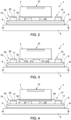
Figure 2 is a cross-section through the microelectromechanical device ofFigure 1 , taken along line II-II ofFigure 1 ; -
Figure 3 is a cross-section through the microelectromechanical device ofFigure 1 , taken along line III-III ofFigure 1 ; -
Figure 4 is a cross-section through a microelectromechanical device according to a different embodiment of the present invention; -
Figure 5 is a top plan view of a microelectromechanical device according to another embodiment of the present invention; -
Figure 6 is a cross-section through the microelectromechanical device ofFigure 5 , taken along line VI-VI ofFigure 5 ; -
Figure 7 is a cross-section through a microelectromechanical device according to a further embodiment of the present invention; -
Figure 8 is a cross-section through a microelectromechanical device according to a different embodiment of the present invention; -
Figures 9-11 illustrate successive steps of a process for manufacturing a microelectromechanical device according to an embodiment of the present invention; and -
Figure 12 is a simplified block diagram of an electronic system incorporating a microelectromechanical device according to the present invention. - With reference to
Figures 1-3 , a microelectromechanical device or MEMS (Micro-Electro-Mechanical System) is indicated as a whole with thenumber 1 and comprises a package, whereof only asubstrate 3, a control die 5 and a microelectromechanical system die or, as will be indicated below for simplicity, MEMS die 7 are shown for simplicity. - The
substrate 3 has a support function and may be, for example, a polymeric material layer or a printed circuit board (PCB). - The
control die 5 is joined to thesubstrate 3 by anadhesive layer 8 and incorporates a dedicated control circuit or ASIC (Application Specific Integrated Circuit) 9, not illustrated herein in detail. The control die 5, in particular thededicated control circuit 9, is functionally coupled to the MEMS die 7 to perform the operations wherefor the MEMS die 7 is designed (in general, the conversion of sensed physical quantities into electrical signals and/or the conversion of electrical signals into physical quantities). The connection between thededicated control circuit 9 and theMEMS die 7, may be obtained by wire bonding and is not illustrated herein for simplicity. - The MEMS die 7 incorporates a
microelectromechanical structure 12, for example a membrane, and for example operates as a piezoelectric, piezoresistive or capacitive pressure sensor. However, the invention should not be construed as limited to these examples, but may be generally exploited when desired for any type of microelectromechanical device, including, in particular, electroacoustic transducers (microphones and speakers). - The
MEMS die 7 is joined to a support structure which, in the embodiment ofFigures 1-3 , is defined by thesubstrate 3 and the control die 5. In particular, the MEMS die 7 is joined to a face of the control die 5 opposite to thesubstrate 3. In other embodiments, not shown, the MEMS die might be joined directly to thesubstrate 3 or to a different intermediate substrate or yet the support structure may be defined by thesole control die 5. - In order to join the
MEMS die 7 to the support structure, themicroelectromechanical device 1 comprises aconnection structure 13. In turn, theconnection structure 13 comprises aspacer structure 15, formed on thecontrol die 5, and afilm 16 applied to one face of thespacer structure 15 opposite to thecontrol die 5. - The
spacer structure 15 is formed for example by a resist layer deposited on thecontrol die 5 and subsequently patterned. In the embodiment ofFigures 1-3 , thespacer structure 15 comprises a first portion, forming anouter frame 17 which laterally delimits acavity 18, and a second portion, which defines ananchor 20 inside thecavity 18. Thecavity 18 is further delimited by the face of thecontrol die 5 on which thespacer structure 15 is formed. In plan, theframe 17 and theanchor 20 may have a polygonal shape, for example square or rectangular. Theframe 17 may not be continuous in some embodiments. In these cases, thecavity 18 is laterally delimited only in part and may communicate with the outside. Thecavity 18 has greater dimensions (width and length) with respect to corresponding dimensions of theMEMS die 7. - The
film 16 in one embodiment is obtained from a dry resist sheet laminated on thespacer structure 15 and subsequently patterned. In particular, thefilm 16 forms aplatform 21 bonded to theanchor 20 and maintained by thesame anchor 20 at least partially suspended on thecavity 18 at a distance from thecontrol die 5. Anouter portion 22 of thefilm 16 may be present on theframe 17 of thespacer structure 15. - In the embodiment of
Figures 1-3 , theplatform 21 is centrally supported by theanchor 20. In detail, theplatform 21 comprises acentral anchor portion 21a supported by theanchor 20, anouter frame 21b andarms 21c projecting from theanchor 20 and connecting thecentral anchor portion 21b to theouter frame 21a. Theouter frame 21a in one embodiment is quadrangular and defines an outer shape of theplatform 21. Theanchor 20, also quadrangular, has dimensions not greater than 300 of corresponding dimensions of theplatform 21. In practice, each side of theanchor 20 is not greater than 30% of a corresponding side of theouter frame 21b of theplatform 21. Thearms 21c have a width comprised between 5% and 15% of a maximum dimension of theplatform 21, for example 10%. - The MEMS die 7 is joined to the
platform 21, more precisely to theouter frame 21b. Like theplatform 21, the MEMS die 7 is also centrally supported by thesole anchor 20 and projects laterally, remaining suspended on thecavity 18. Since the dimensions (width and length) of thecavity 18 are greater than the corresponding dimensions of theMEMS die 7, the MEMS die may be arranged so that it is not superimposed on theframe 17 of thespacer structure 15. - In the embodiment described, the mechanical connection between the
MEMS die 7 and the support structure, in this case formed by thesubstrate 3 and thecontrol die 5, is limited to theanchor 20. Since the dimensions of theanchor 20 are small and significantly smaller with respect to the dimensions of theMEMS die 7, the deformations and stresses whereto the support structure is subject are not conveyed, or at least are conveyed to a negligible extent, to theMEMS die 7. Consequently, the operation of theMEMS die 7 is not affected by the effects of the deformations and the stresses induced by outer factors, for example of thermomechanical origin, to the advantage of the accuracy. - The dimensions of the
platform 21 may be conveniently chosen so that the placing of theMEMS die 7 may be carried out accurately and without difficulty. - In one embodiment (
Figure 4 ), thecavity 18 is filled with asealing gel 25, for example potting gel. The sealinggel 25 makes thecavity 18 impermeable and protects thededicated control circuit 9 from humidity. The sealing gel may cover theplatform 21. In this case, a thin gel layer may be interposed between theplatform 21 and the MEMS die 7. - According to an embodiment of the invention, illustrated in
Figures 5 and6 , amicroelectromechanical device 100 comprises a package, whereof only asubstrate 103, a control die 105 and a MEMS die 107 are shown for simplicity. Thesubstrate 103 and the control die 5 are joined to each other, for example by anadhesive layer 108, and form a support structure for the MEMS die 107, substantially as already described. - The MEMS die 107 incorporates a
microelectromechanical structure 112, here again of the membrane type, and for example operates as an electroacoustic transducer (microphone or loudspeaker). - The
microelectromechanical device 100 comprises aconnection structure 113 which joins the MEMS die 107 to the support structure, in particular to the control die 105. In turn, theconnection structure 113 comprises aspacer structure 115, formed on the control die 105, and afilm 116 applied to one face of thespacer structure 115 opposite to the control die 105. Thespacer structure 115 forming a frame which laterally delimits acavity 118, having greater dimensions (width and length) with respect to corresponding dimensions of the MEMS die 107. - The
film 116 is obtained from a dry resist sheet laminated on thespacer structure 115 and subsequently patterned. In particular, thefilm 116 forms aplatform 121 bonded to ananchor 120, defined by a portion, for example one side, of thespacer structure 115. Theplatform 121 is supported laterally by theanchor 120 and maintained by thesame anchor 120 at least partially suspended on thecavity 118 at a distance from the control die 105. More precisely, thefilm 116 comprises ananchor portion 116a supported by theanchor 120 and anarm 116b which connects theanchor portion 116a to an outer side of theplatform 121, which is frame-shaped and has a central opening. - The MEMS die 107 is joined to the
platform 121 and is therefore supported laterally with respect to theanchor 120, above thecavity 118. The support for the MEMS die 107 in this case is provided exclusively by theplatform 121 and thearm 116b which connects theplatform 121 to theanchor portion 116 of thefilm 116. The width and length of thearm 116b, in particular, may be selected so that thesame arm 116b has sufficient stiffness to support the MEMS die 107. - In this case, the MEMS die 107 is completely insensitive to the deformations of the support structure and the functioning is not affected, in particular, by the thermomechanical stresses and residual stresses that might be conveyed through the support structure. The
platform 121, in fact, is connected to theanchor 120 only through thearm 116b and the MEMS die 107 does not overlap at any point on thespacer structure 115. The deformations of the support structure may at most slightly modify the relative position of theplatform 121 and the MEMS die 107 with respect to the same support structure, but the strains are not conveyed. - Also in this case, the
cavity 118 may be filled with a sealinggel 125, as shown in the embodiment ofFigure 7 . - With reference to
Figure 8 , in one embodiment of the present invention amicroelectromechanical device 200 may comprise a package with asubstrate 203, a control die 205, a MEMS die 207, incorporating amicroelectromechanical structure 212, and aconnection structure 213 which joins the MEMS die 207 to the support structure formed by thesubstrate 203 and the control die 205 joined to each other. Theconnection structure 213 comprises a frame-shapedspacer structure 215, formed on the control die 205 and delimiting acavity 218, and afilm 216 applied to one face of thespacer structure 215 opposite to the control die 205. Thefilm 216 in this case is continuous and closes thecavity 218, which has a length and width greater than the length and width of the MEMS die 207. - The MEMS die 207 is joined to the
film 216 above thecavity 218 and is therefore suspended without overlapping thespacer structure 215. -
Figures 9-11 summarily show an example of a process for manufacturing a microelectromechanical device according to the invention, in particular the microelectromechanical device ofFigures 1-3 . - In a
semiconductor wafer 300 thededicated control circuit 9 is initially provided, then aspacer layer 301 of resist is deposited and patterned by a first photolithographic process to form thespacer structure 15, including theanchor 20. - The film 16 (
Figure 10 ) of dry resist is laminated on thewafer 300 and adheres to thespacer structure 15 which projects. - The
film 16 is defined with a second photolithographic process to form the platform 21 (Figure 11 ) and the MEMS die 7, provided separately from a different semiconductor wafer not shown, is joined to theplatform 21. Thewafer 300 is then diced and the composed dice obtained are joined torespective substrates 3, to form themicroelectromechanical device 1 ofFigures 1-3 . - Alternatively, before joining the MEMS die 7, the cavity is filled with the sealing
gel 25, to obtain the structure ofFigure 4 . - The structures of
Figures 5-6 andFigure 7 may be provided with the same process, simply by using photolithographic masks with the desired pattern. - In order to provide the
microelectromechanical device 200 ofFigure 8 , the MEMS die 207 is joined to thefilm 216 without having carried out the second photolithographic process. -
Figure 12 shows anelectronic system 400 which may be of any type, in particular, but not limited to, a wearable device, such as a watch, a bracelet or a "smart" band; a computer, such as a mainframe, a personal computer, a laptop, or a tablet; a smartphone; a digital music player, a digital camera or any other device for processing, storing, transmitting or receiving information. Theelectronic system 400 may be a general purpose or device-embedded processing system, an equipment or a further system. - The
electronic system 400 comprises aprocessing unit 402,memory devices 403, a microelectromechanical device according to the invention, for example the microelectromechanical device (pressure sensor) 1 ofFigure 1 , and may also be provided with input/output (I/O) devices 405 (for example a keyboard, a pointer or a touch screen), awireless interface 406, peripherals 407.1, ..., 407.N and possibly further auxiliary devices, not shown here. The components of theelectronic system 400 may be coupled in communication with each other directly and/or indirectly through abus 408. Theelectronic system 400 may further comprise abattery 409. It should be noted that the scope of the present invention is not limited to embodiments necessarily having one or all of the listed devices. - The
processing unit 402 may comprise, for example, one or more microprocessors, microcontrollers and the like, according to the design preferences. - The
memory devices 403 may comprise volatile memory devices and non-volatile memory devices of various kinds, for example SRAM and/or DRAM memories for volatile memories and solid-state memories, magnetic disks and/or optical disks for non-volatile memories. - Finally, it is apparent that modifications and variations may be made to the described microelectromechanical device, without departing from the scope of the present invention, as defined in the attached claims.
- In particular, it is understood that all the connection structures described may be used with microelectromechanical devices of any type, both of membrane type and other types, according to the design preferences.
- The support structure may be of any suitable type in addition to those described. For example, the MEMS die may be joined directly to a portion of the package, without the interposition of the control die and any suitable part of the packaging may function as a support structure. Conversely, other components may be interposed between the MEMS die and the packaging or the control die (for example, another die).
Claims (17)
- A microelectromechanical device comprising:a support structure (3, 5; 103, 105; 203, 205);a microelectromechanical system die (7; 107; 207) incorporating a microstructure (12; 112; 212);a connection structure (13; 113; 213) between the microelectromechanical system die (7; 107; 207) and the support structure (3, 5; 103, 105; 203, 205);wherein the connection structure (13; 113; 213) comprises a spacer structure (15; 115; 215), joined to the support structure (3, 5; 103, 105; 203, 205), and a film (16; 116; 216) applied to a face of the spacer structure (15; 115; 215) opposite to the support structure (3, 5; 103, 105; 203, 205);wherein the spacer structure (15; 115; 215) laterally delimits at least in part a cavity (18; 118; 218) and the film (16; 116; 216) extends on the cavity (18; 118; 218), at a distance from the support structure (3, 5; 103, 105; 203, 205) ;and wherein the microelectromechanical system die (7; 107; 207) is joined to the film (16; 116; 216) on the cavity (18; 118; 218).
- The device according to claim 1, wherein the film (16; 116; 216) is of dry resist.
- The device according to claim 1 or 2, wherein the microelectromechanical system die (7; 107; 207) extends on the cavity (18; 118; 218) without overlapping the spacer structure (15; 115; 215) around the cavity (18; 118; 218).
- The device according to any of the preceding claims, wherein the film (16; 116) defines a platform (21; 121) extending on the cavity (18; 118) and the microelectromechanical system die (7; 107) is joined to the platform (21; 121).
- The device according to claim 4, wherein the cavity (18; 118) is filled with a sealing gel (25; 125).
- The device according to any of the preceding claims, the platform (21; 121) is maintained suspended by an anchor (20; 120) .
- The device according to claim 6, wherein the anchor (20; 120) is defined by an anchor portion (20; 120) of the spacer structure (15; 115).
- The device according to claim 6 or 7, wherein the platform (21) is centrally supported by the anchor (20).
- The device according to any of claims 6 to 8, wherein the platform (21) comprises a central anchor portion (21a) supported by the anchor (20), an outer frame (21b) and arms (21c) projecting from the anchor (20; 120) and connecting the central anchor portion (21a) to the outer frame (21b).
- The device according to claim 6, wherein the platform (121) is supported laterally by the anchor (120).
- The device according to claim 6 or 10, wherein the film (116) comprises an anchor portion (116a) supported by the anchor (120) and at least one arm (116b) connecting the anchor portion (116a) to the platform (121).
- The device according to claim 11, wherein the platform (121) is frame-shaped and wherein an outer side of the platform (121) is connected to the anchor portion (116a) of the film (116) by the at least one arm (116b).
- The device according to any of the preceding claims, wherein the support structure (3, 5; 103, 105; 203, 205) comprises a substrate (3; 103; 203) and a control die (5; 105; 205), joined to the substrate and functionally coupled to the microstructure (12; 112; 212) of the microelectromechanical system die (7; 107; 207) and wherein the connection structure (13; 113; 213) joins the microelectromechanical system die (7; 107; 207) to the control die (5; 105; 205).
- An electronic system comprising a processing unit (402) and a microelectromechanical device (1) according to any of the preceding claims.
- The system according to claim 14, wherein the microelectromechanical device (1) is a membrane device, in particular one of a pressure sensor and an electroacoustic transducer.
- A process for manufacturing a microelectromechanical device, comprising:depositing a spacer layer (301) of resist on a semiconductor wafer (300);from the spacer layer (301), forming a spacer structure (15) laterally delimiting at least in part a cavity (18);applying a film (16) to the semiconductor wafer (300), so that it adheres to the spacer structure (15);joining a microelectromechanical system die (7) incorporating a microelectromechanical structure to the film (16) on the cavity (18).
- The process according to claim 16, wherein the film (16) is of dry resist and is defined with a photolithographic process before joining the microelectromechanical system die (7) .
Applications Claiming Priority (1)
| Application Number | Priority Date | Filing Date | Title |
|---|---|---|---|
| IT102022000009488A IT202200009488A1 (en) | 2022-05-09 | 2022-05-09 | MICROELECTROMECHANICAL DEVICE AND PROCEDURE FOR MANUFACTURING A MICROELECTROMECHANICAL DEVICE |
Publications (2)
| Publication Number | Publication Date |
|---|---|
| EP4276056A1 true EP4276056A1 (en) | 2023-11-15 |
| EP4276056A9 EP4276056A9 (en) | 2023-12-27 |
Family
ID=82385264
Family Applications (1)
| Application Number | Title | Priority Date | Filing Date |
|---|---|---|---|
| EP23170279.6A Pending EP4276056A1 (en) | 2022-05-09 | 2023-04-27 | Microelectromechanical device and process for manufacturing a microelectromechanical device |
Country Status (3)
| Country | Link |
|---|---|
| US (1) | US20230356999A1 (en) |
| EP (1) | EP4276056A1 (en) |
| IT (1) | IT202200009488A1 (en) |
Families Citing this family (1)
| Publication number | Priority date | Publication date | Assignee | Title |
|---|---|---|---|---|
| IT202300025878A1 (en) * | 2023-12-04 | 2025-06-04 | St Microelectronics Int Nv | SEALED MEMBRANE MICROELECTROMECHANICAL DEVICE |
Citations (2)
| Publication number | Priority date | Publication date | Assignee | Title |
|---|---|---|---|---|
| JP2010272548A (en) * | 2007-09-06 | 2010-12-02 | Alps Electric Co Ltd | Device mounting module and manufacturing method thereof |
| CN205709848U (en) * | 2016-05-24 | 2016-11-23 | 清华大学 | Mems sensor structure |
-
2022
- 2022-05-09 IT IT102022000009488A patent/IT202200009488A1/en unknown
-
2023
- 2023-04-27 EP EP23170279.6A patent/EP4276056A1/en active Pending
- 2023-04-27 US US18/308,562 patent/US20230356999A1/en active Pending
Patent Citations (2)
| Publication number | Priority date | Publication date | Assignee | Title |
|---|---|---|---|---|
| JP2010272548A (en) * | 2007-09-06 | 2010-12-02 | Alps Electric Co Ltd | Device mounting module and manufacturing method thereof |
| CN205709848U (en) * | 2016-05-24 | 2016-11-23 | 清华大学 | Mems sensor structure |
Also Published As
| Publication number | Publication date |
|---|---|
| EP4276056A9 (en) | 2023-12-27 |
| US20230356999A1 (en) | 2023-11-09 |
| IT202200009488A1 (en) | 2023-11-09 |
Similar Documents
| Publication | Publication Date | Title |
|---|---|---|
| US10605684B2 (en) | Multi-transducer modulus, electronic apparatus including the multi-transducer modulus and method for manufacturing the multi-transducer modulus | |
| EP3330689B1 (en) | Multi-device transducer modulus, electronic apparatus including the transducer modulus and method for manufacturing the transducer modulus | |
| EP3248936A1 (en) | Mems pressure sensor and mems inertial sensor integration structure | |
| KR101807064B1 (en) | Microphone system and manufacturign the same | |
| US10329141B2 (en) | Encapsulated device of semiconductor material with reduced sensitivity to thermo-mechanical stresses | |
| US10593861B2 (en) | Electronic component having a reinforced hollowed structure | |
| US7763972B2 (en) | Stacked package structure for reducing package volume of an acoustic micro-sensor | |
| CN104555887B (en) | Microelectromechanical device with protection for bonding and process for manufacturing a microelectromechanical device | |
| US9975756B2 (en) | Micro-electro-mechanical pressure device and methods of forming same | |
| EP4276056A9 (en) | Microelectromechanical device and process for manufacturing a microelectromechanical device | |
| US10312880B2 (en) | Method for manufacturing electronic component module | |
| CN220766507U (en) | Electronic equipment | |
| US20200236471A1 (en) | Microphone | |
| US9510495B2 (en) | Electronic devices with cavity-type, permeable material filled packages, and methods of their manufacture | |
| JP2007178133A (en) | Pressure sensor module, manufacturing method thereof, and semiconductor device | |
| US20090141913A1 (en) | Microelectromechanical system | |
| US6308575B1 (en) | Manufacturing method for the miniaturization of silicon bulk-machined pressure sensors | |
| JP5343678B2 (en) | Semiconductor device and manufacturing method thereof | |
| JP5771921B2 (en) | SEALED DEVICE AND MANUFACTURING METHOD THEREOF | |
| US11760627B2 (en) | MEMS stress reduction structure embedded into package | |
| WO2018218670A1 (en) | Fingerprint chip packaging module, fingerprint recognition module and packaging method | |
| EP4567395A1 (en) | Sealed microelectromechanical membrane device | |
| US20210025774A1 (en) | Pressure Sensor | |
| JP2003078997A (en) | Electret condenser microphone | |
| JPH07243928A (en) | Physical quantity measuring sensor, manufacturing method thereof, and multilayer circuit board |
Legal Events
| Date | Code | Title | Description |
|---|---|---|---|
| PUAI | Public reference made under article 153(3) epc to a published international application that has entered the european phase |
Free format text: ORIGINAL CODE: 0009012 |
|
| STAA | Information on the status of an ep patent application or granted ep patent |
Free format text: STATUS: THE APPLICATION HAS BEEN PUBLISHED |
|
| AK | Designated contracting states |
Kind code of ref document: A1 Designated state(s): AL AT BE BG CH CY CZ DE DK EE ES FI FR GB GR HR HU IE IS IT LI LT LU LV MC ME MK MT NL NO PL PT RO RS SE SI SK SM TR |
|
| STAA | Information on the status of an ep patent application or granted ep patent |
Free format text: STATUS: REQUEST FOR EXAMINATION WAS MADE |
|
| 17P | Request for examination filed |
Effective date: 20240515 |
|
| RBV | Designated contracting states (corrected) |
Designated state(s): AL AT BE BG CH CY CZ DE DK EE ES FI FR GB GR HR HU IE IS IT LI LT LU LV MC ME MK MT NL NO PL PT RO RS SE SI SK SM TR |