EP4273744A1 - Fingerprint module and electronic device - Google Patents
Fingerprint module and electronic device Download PDFInfo
- Publication number
- EP4273744A1 EP4273744A1 EP21914271.8A EP21914271A EP4273744A1 EP 4273744 A1 EP4273744 A1 EP 4273744A1 EP 21914271 A EP21914271 A EP 21914271A EP 4273744 A1 EP4273744 A1 EP 4273744A1
- Authority
- EP
- European Patent Office
- Prior art keywords
- light
- display module
- fingerprint module
- support component
- refractive index
- Prior art date
- Legal status (The legal status is an assumption and is not a legal conclusion. Google has not performed a legal analysis and makes no representation as to the accuracy of the status listed.)
- Pending
Links
Images


Classifications
-
- G—PHYSICS
- G06—COMPUTING OR CALCULATING; COUNTING
- G06V—IMAGE OR VIDEO RECOGNITION OR UNDERSTANDING
- G06V40/00—Recognition of biometric, human-related or animal-related patterns in image or video data
- G06V40/10—Human or animal bodies, e.g. vehicle occupants or pedestrians; Body parts, e.g. hands
- G06V40/12—Fingerprints or palmprints
- G06V40/13—Sensors therefor
- G06V40/1318—Sensors therefor using electro-optical elements or layers, e.g. electroluminescent sensing
-
- G—PHYSICS
- G06—COMPUTING OR CALCULATING; COUNTING
- G06V—IMAGE OR VIDEO RECOGNITION OR UNDERSTANDING
- G06V40/00—Recognition of biometric, human-related or animal-related patterns in image or video data
- G06V40/10—Human or animal bodies, e.g. vehicle occupants or pedestrians; Body parts, e.g. hands
- G06V40/12—Fingerprints or palmprints
- G06V40/13—Sensors therefor
- G06V40/1324—Sensors therefor by using geometrical optics, e.g. using prisms
-
- G—PHYSICS
- G06—COMPUTING OR CALCULATING; COUNTING
- G06V—IMAGE OR VIDEO RECOGNITION OR UNDERSTANDING
- G06V40/00—Recognition of biometric, human-related or animal-related patterns in image or video data
- G06V40/10—Human or animal bodies, e.g. vehicle occupants or pedestrians; Body parts, e.g. hands
- G06V40/12—Fingerprints or palmprints
- G06V40/13—Sensors therefor
- G06V40/1329—Protecting the fingerprint sensor against damage caused by the finger
Definitions
- This application relates to the field of communication technologies, and in particular to a fingerprint module and an electronic device.
- the electronic device includes a fingerprint module and a display module.
- the fingerprint module is disposed below the display module, and the display module emits light. After the light is refracted by a user's finger, part of the light enters the fingerprint module, to recognize a user's fingerprint.
- a microlens film may be pasted on a photosensitive unit of the fingerprint module. The microlens film can change scattered light into parallel light, improving the optical performance of the fingerprint module.
- Embodiments of this application are intended to provide a fingerprint module and an electronic device, which can resolve a problem of poor imaging quality of the fingerprint module.
- an embodiment of this application provides a fingerprint module.
- the fingerprint module is used in an electronic device and includes a photosensitive unit, a microlens film, and a support component.
- the photosensitive unit and a display module of the electronic device are disposed opposite to each other.
- the microlens film is disposed between the photosensitive unit and the display module.
- a first distance between the support component and the display module is smaller than a second distance between the microlens film and the display module.
- the assembly gap has a first refractive index
- the display module has a second refractive index
- the microlens film has a third refractive index.
- the first refractive index is different from the second refractive index
- the first refractive index is different from the third refractive index.
- an electronic device includes a light-transmitting cover plate, a display module, and the foregoing fingerprint module.
- the light-transmitting cover plate covers the display module, and the fingerprint module is located on a side, away from the light-transmitting cover plate, of the display module.
- a first surface, facing the display module, of a microlens film is provided with a support component.
- a first distance between the support component and the display module is smaller than a second distance between the microlens film and the display module.
- Embodiments of this application disclose a fingerprint module 100.
- the fingerprint module 100 is used in an electronic device, to achieve a fingerprint recognition function of the electronic device.
- the disclosed fingerprint module 100 includes a photosensitive unit 110, a microlens film 120, and a support component 130.
- the photosensitive unit 110 is configured to receive an optical signal and can convert the optical signal into image information.
- the photosensitive unit 110 and a display module 200 of the electronic device are disposed opposite to each other.
- the microlens film 120 can collimate light, to change scattered light into parallel light, reducing waste of light. This increases light entering the photosensitive unit 110 and improves working performance of the photosensitive unit 110.
- a first surface, facing the display module 200, of the microlens film 120 is provided with the support component 130.
- a first distance between the support component 130 and the display module 200 is smaller than a second distance between the microlens film 120 and the display module 200.
- the assembly gap 140 has a first refractive index
- the display module 200 has a second refractive index
- the microlens film 120 has a third refractive index.
- the first refractive index is different from the second refractive index
- the first refractive index is different from the third refractive index.
- the fingerprint module 100 works, light passes through the display module 200, passes through the microlens film 120, and then enters the photosensitive unit 110. After passing through a photodiode in the photosensitive unit 110, a light signal is converted into an electrical signal. The electrical signal is converted by an operational amplifier and ADC to generate a digital image signal. The digital image signal is processed by a processor in the electronic device to generate a fingerprint texture image.
- the assembly gap 140 is filled with air. Therefore, the first refractive index may a refractive index of the air. When the first distance between the support component 130 and the display module 200 is zero, the support component 130 contacts the display module 200. When the first distance between the support component 130 and the display module 200 is greater than zero, the display module 200 without deformation does not contact the support component 130.
- the first refractive index may be smaller than the second refractive index and smaller than the third refractive index.
- the assembly gap 140 may also be filled with an inert gas, or the assembly gap 140 is in a vacuum state. Similarly, the first refractive index may also be smaller than the second refractive index and smaller than the third refractive index.
- the display module 200 when the display module 200 is deformed, the display module 200 contacts the support component 130, but does not directly contact the microlens film 120. Therefore, after light passes through the display module 200, because the refractive index of the assembly gap 140 is different from the refractive index of the display module 200 and the refractive index of the microlens film 120, large-angle light is easily refracted or reflected when entering the microlens film 120, and then it is difficult for the large-angle light to form interference fringes, to improve imaging quality of the fingerprint module 100.
- the support component 130 can enhance bending resistance of the display module 200, preventing the display module 200 from being damaged due to excessive deformation.
- one end of the support component 130 may be disposed on the first surface, and a second end of the support component 130 may be a first free end.
- the first free end can contact the display module 200.
- the first distance is greater than zero.
- the first distance can play a buffering role, so that a stress between the display module 200 and the fingerprint module 100 is relatively small, and the fingerprint module 100 and the display module 200 are not easily damaged.
- the support component 130 and the microlens film 120 may be made of a same light-transmitting material, or the support component 130 and the microlens film 120 may be made of different light-transmitting materials, which is not limited herein.
- the support component 130 may have a plurality of structures.
- the support component 130 may be a cylinder, a circular truncated cone, a polygonal cylinder, or a polygonal cone-like structure.
- the support component 130 may also have another structure, which is not limited herein.
- a support area of the support components 130 is further increased, further preventing the display module 200 from contacting the microlens film 120.
- a support force for the display module 200 is further increased, further improving bending resistance of the display module 200.
- the plurality of support components 130 may be arranged in an array on the first surface, and outer surfaces of the support components 130 are provided with first color filter layers. According to common general knowledge, it can be known that light intensity of different wavelengths reflected by a finger and another object is different. Therefore, the finger and the another object can be distinguished by a difference in light intensity of different wavelengths by using the first color filter layer, to achieve anti-counterfeiting detection of an optical path and further improve reliability of the electronic fingerprint module 100.
- colors of filtered light corresponding to the first color filter layers of two adjacent support components 130 are different.
- the first color filter layers can detect light with different wavelengths, further improving reliability of the anti-counterfeiting detection.
- the colors of the first color filter layers may include red, blue, and green. Therefore, the colors are alternately arranged based on three primary colors. Of course, other colors may also be selected, which is not limited herein.
- the photosensitive unit 110 may have a plurality of pixel regions 111.
- the plurality of pixel regions 111 may be arranged at intervals, and at least one support component 130 may be disposed in a region that is corresponding to each pixel region 111 and that is on the first surface.
- an orthographic projection of the at least one support component 130 may be located in the pixel region 111 corresponding to the support component 130.
- the support component 130 affects only the pixel region 111 corresponding to the support component 130, and does not affect other pixel regions 111. Therefore, an influence on entire fingerprint imaging is reduced.
- the orthographic projection of the at least one support component 130 coincides with the pixel region 111 corresponding to the support component 130.
- a cross-sectional area of the pixel region 111 is the same as a cross-sectional area of the support component 130, to better facilitate design and manufacturing of the photosensitive unit.
- N ⁇ N support components 130 form a first sub-array, and the first sub-array corresponds to one pixel region 111.
- N ⁇ N light condensing protrusions 122 form a second sub-array, and the second sub-array corresponds to one pixel region 111.
- At least one second sub-array is disposed between two adjacent first sub-arrays. Colors of first color filter layers disposed on support components 130 in a same first sub-array are the same. Colors of first color filter layers disposed on support components 130 in two adjacent first sub-arrays may be different.
- the first sub-array can be a 2 ⁇ 2 array group, and the second sub-array may also be a 2 ⁇ 2 array group.
- the first sub-array and the second sub-array may also be other array groups, such as 3 ⁇ 3 array groups, 4 ⁇ 4 array groups, which is not limited in herein.
- a filling structure may be disposed in the assembly gap 140.
- a third surface of the filling structure is connected to the first surface
- a fourth surface of the filling structure is connected to the display module 200
- a refractive index of the filling structure is the first refractive index.
- the filling structure is filled in the assembly gap 140, to support the display module 200, improving bending resistance of the display module 200 and preventing the display module 200 from being deformed.
- the filling structure improves the bending resistance of the display module 200. Therefore, a distance between the fingerprint module 100 and the display module 200 can be reduced, that is, the assembly gap 140 is reduced, reducing an overall thickness of the electronic device.
- the support component 130 may be embedded in the filling structure.
- the support component 130 may provide an auxiliary support for the display module 200, to prevent the display module 200 from being further deformed.
- the support component 130 may be constituted by the filling structure, and the refractive index of the filling structure is the first refractive index.
- the support component 130 is filled in the assembly gap 140, so that the support component 130 has a simple structure and a large support range.
- the filling structure may be made of a material with a relatively low refractive index.
- the filling structure may be UV glue.
- the UV glue is normally liquid and is cured after being irradiated by violet light (or ultraviolet light), so that the filling structure is easily bonded and processed.
- the cured UV glue has good adhesiveness, and can further enhance reliability of the electronic device.
- the filling material may also be another organic composite material, and a specific material of the filling structure is not limited herein.
- the microlens film 120 may have a plurality of light condensing protrusions 122.
- the plurality of light condensing protrusions 122 are arranged in an array on the first surface.
- the light condensing protrusions 122 are equivalent to convex lenses, and can further change scattered light into parallel light, increasing light entering the photosensitive unit 110 and further improving working performance of the photosensitive element.
- the plurality of light condensing protrusions 122 are arranged in an array on the first surface. Therefore, the light condensing protrusions 122 are arranged more regularly and have relatively compact structures.
- the microlens film further includes a substrate 121, and the light condensing protrusions 122 are disposed on the substrate 121.
- the substrate 121 may be made of a PET (polyethyleneterephthalate) material, of course, may be alternatively made of another material, which is not limited herein.
- the plurality of support components 130 and the plurality of light condensing protrusions 122 may be arranged in an array on the first surface.
- N ⁇ N support components 130 form a first sub-array
- N ⁇ N light condensing protrusions 122 form a second sub-array.
- Each first sub-array corresponds to one pixel point in the display module 200
- each second sub-array corresponds to one pixel point in the display module 200, where N is a positive integer greater than or equal to 1.
- the support component 130 affects only a pixel point corresponding to the support component 130, and does not affect other pixel points. Therefore, an influence on entire fingerprint imaging is reduced.
- a plurality of first light-transmitting holes 131 may be disposed on the support component 130. Axes of the first light-transmitting holes 131 are perpendicular to the display module 200 and the microlens film 120. In this case, light passes through the first light-transmitting holes 131 and then enters the microlens film 120. In this solution, a sidewall of the first light-transmitting hole 131 can absorb and block stray light, reducing interference of light between collimating holes on the microlens film 120.
- the plurality of light condensing protrusions 122 are arranged to be in a one-to-one correspondence with the plurality of first light-transmitting holes 131.
- light in the first light-transmitting hole 131 is reflected by a corresponding light condensing protrusion 122, further reducing interference between light.
- an orthographic projection of the light condensing protrusion 122 is within an outline of an orthographic projection of the first light-transmitting hole 131, or an orthographic projection of the light condensing protrusion 122 coincides with an orthographic projection of the first light-transmitting hole 131.
- the light condensing protrusion 122 may be within the first light-transmitting hole 131, further reducing the interference between light and ensuring a good light shading effect.
- the support component 130 may be made of a black film material, achieving light shielding.
- the support component 130 is made of a material that can well absorb visible light or full wave-band light.
- the first light-transmitting hole 131 is coated with an ink coating to achieve light shielding.
- the support component 130 may have a honeycomb structure.
- a connecting side wall between two adjacent first light-transmitting holes 131 is a light-shielding part of the first light-transmitting hole 131. Therefore, the side wall between two adjacent first light-transmitting holes 131 should be set thinner, which may not easily affect imaging of the fingerprint module 100.
- the fingerprint module 100 may further include a light-shielding layer 123.
- the light-shielding layer 123 may be disposed on a second surface, facing the photosensitive unit 110, of the microlens film 120.
- a plurality of second light-transmitting holes may be disposed on light-shielding layer 123. Each second light-transmitting hole is disposed opposite to one support component 130 or one light condensing protrusion 122.
- the light-shielding layer 123 can shield and absorb large-angle light refracted by the support component 130, preventing influence of the large-angle light on imaging.
- the light-shielding layer 123 may be an ink coating coated on the second surface, and of course may also be another light-shielding material, which is not limited herein.
- a support column 132 is further disposed in the first light-transmitting hole 131.
- a first end of the support column 132 is connected to the first surface, and a second end of the support column 132 is a second free end.
- the support column 132 can support the display module 200, preventing the display module 200 from contacting the microlens film 120, and improving reliability of the fingerprint module 100.
- a shape of the support column 132 matches a shape of the first light-transmitting hole 131, so that matching performance between the first light-transmitting hole 131 and the support column 132 is improved.
- the support column 132 may be coated with a second color filter layer, achieving anti-counterfeiting detection of an optical path of the fingerprint module 100, further improving reliability of the fingerprint module 100.
- a manner in which the second color filter layer is disposed is the same as a manner in which the first color filter layer is disposed. The details are not described herein again.
- the fingerprint module 100 may further include an optical filter 160.
- the optical filter 160 may be disposed between the photosensitive unit 110 and the microlens film 120.
- the optical filter 160 can absorb light with different wavelengths, filtering out light with different wavelengths, further obtaining light required for fingerprint imaging and improving reliability of fingerprint recognition.
- an embodiment of this application further discloses an electronic device.
- the disclosed electronic device includes the fingerprint module 100 in any one of the foregoing embodiments.
- the electronic device disclosed in this embodiment of this application may further include a light-transmitting cover plate 300 and a display module 200.
- the light-transmitting cover plate 300 can cover the display module 200, and the fingerprint module 100 is located on a side, away from the light-transmitting cover plate 300, of the display module 200.
- the display module 200 contacts a support component 130, but not directly contact a microlens film 120.
- a refractive index of an assembly gap 140 is different from ta refractive index of the display module 200 and a refractive index of the microlens film 120, large-angle light is easily refracted or reflected when entering the microlens film 120, and then it is difficult for the large-angle light to form interference fringes, to improve reliability of the fingerprint module 100.
- the light-transmitting cover plate 300 can protect the display module 200, preventing the display module 200 from being damaged. Further, it can be said that the light-transmitting cover plate 300 increases a thickness of the display module 200, improving rigidity of the display module 200, further improving bending resistance of the display module 200.
- the electronic device disclosed in this embodiment of this application may be a smart watch, smart phone, tablet computer, or another device, and a specific type of the electronic device is not limited in this embodiment of this application.
Landscapes
- Engineering & Computer Science (AREA)
- Physics & Mathematics (AREA)
- Human Computer Interaction (AREA)
- General Physics & Mathematics (AREA)
- Multimedia (AREA)
- Theoretical Computer Science (AREA)
- Optics & Photonics (AREA)
- Image Input (AREA)
- Solid State Image Pick-Up Elements (AREA)
Abstract
Description
- This application claims priority to
Chinese Patent Application No. 202011640141.1, filed with the Chinese Patent Office on December 31, 2020 - This application relates to the field of communication technologies, and in particular to a fingerprint module and an electronic device.
- With the rapid development of electronic devices, the electronic devices are used increasingly widely, for example, mobile phones, tablet computers, and the like play a growing number of roles in people's work, life, entertainment, and the like.
- In the related art, the electronic device includes a fingerprint module and a display module. The fingerprint module is disposed below the display module, and the display module emits light. After the light is refracted by a user's finger, part of the light enters the fingerprint module, to recognize a user's fingerprint. To improve optical performance of the fingerprint module, a microlens film may be pasted on a photosensitive unit of the fingerprint module. The microlens film can change scattered light into parallel light, improving the optical performance of the fingerprint module.
- While the present invention is achieved, the inventor finds that the related art has the following problems: When a user performs fingerprint unlock, the display module is easily deformed, causing the display module to contact a top of the microlens film. This enables large-angle light passing through the microlens to interfere with each other and form interference fringes, further affecting a fingerprint image, and resulting in poor imaging quality of the fingerprint module.
- Embodiments of this application are intended to provide a fingerprint module and an electronic device, which can resolve a problem of poor imaging quality of the fingerprint module.
- To resolve the foregoing technical problem, this application is implemented as follows.
- According to a first aspect, an embodiment of this application provides a fingerprint module. The fingerprint module is used in an electronic device and includes a photosensitive unit, a microlens film, and a support component.
- The photosensitive unit and a display module of the electronic device are disposed opposite to each other. The microlens film is disposed between the photosensitive unit and the display module. There is an assembly gap between the microlens film and the display module, and the support component is disposed on a first surface of the microlens film facing the display module. A first distance between the support component and the display module is smaller than a second distance between the microlens film and the display module.
- The assembly gap has a first refractive index, the display module has a second refractive index, and the microlens film has a third refractive index. The first refractive index is different from the second refractive index, and the first refractive index is different from the third refractive index.
- According to a second aspect, an electronic device is provided. The electronic device includes a light-transmitting cover plate, a display module, and the foregoing fingerprint module. The light-transmitting cover plate covers the display module, and the fingerprint module is located on a side, away from the light-transmitting cover plate, of the display module.
- In this embodiment of this application, a first surface, facing the display module, of a microlens film is provided with a support component. A first distance between the support component and the display module is smaller than a second distance between the microlens film and the display module. In other words, when the display module is deformed, the display module contacts the support component, but does not directly contact the microlens film. Therefore, after light passes through the display module, because a refractive index of an assembly gap is different from a refractive index of the display module and a refractive index of the microlens film, large-angle light is easily refracted or reflected when entering the microlens film, and then it is difficult for the large-angle light to form interference fringes, to improve imaging quality of the fingerprint module.
-
-
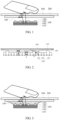
FIG 1 is a first schematic diagram of a structure of an electronic device according to an embodiment of this application; -
FIG 2 is a schematic diagram of a structure of a bent display module in the first electronic device according to an embodiment of this application; -
FIG 3 is a second schematic diagram of a structure of an electronic device according to an embodiment of this application; -
FIG 4 is a third schematic diagram of a structure of an electronic device according to an embodiment of this application; -
FIG 5 is a fourth schematic diagram of a structure of an electronic device according to an embodiment of this application; -
FIG 6 is a fifth schematic diagram of a structure of an electronic device according to an embodiment of this application; -
FIG 7 is a schematic diagram of a structure of a microlens film and a support component in a fingerprint module according to an embodiment of this application; -
FIG 8 is a schematic diagram of a structure of a fingerprint module according to an embodiment of this application; -
FIG 9 is a schematic diagram of a structure of a microlens film in a fingerprint module according to an embodiment of this application; and -
FIG 10 is a top view of a support component inFIG 5 and FIG 6 . - Reference numerals:
- 100-fingerprint module, 110-photosensitive unit, 111-pixel region, 120-microlens film, 121-substrate, 122-light condensing protrusion, 123-light-shielding layer, 130-support component, 131-first light-transmitting hole, 132-support column, 140-assembly gap, 150-filling structure, 160-optical filter,
- 200-display module,
- 300-light-transmitting cover plate
- The following clearly and completely describes the technical solutions in the embodiments of this application with reference to the accompanying drawings in the embodiments of this application. Apparently, the described embodiments are some rather than all of the embodiments of this application. Based on the embodiments of this application, all other embodiments obtained by a person of ordinary skill in the art without creative efforts fall within the protection scope of this application.
- Terms "first" and "second" in the specification and claims of this application are used to distinguish between similar objects, and do not need to be used to describe a specific order or sequence. It should be understood that the data used in this way is interchangeable in appropriate circumstances so that the embodiments of this application described can be implemented in other orders than the order illustrated or described herein. In addition, in the specification and the claims, "and/or" represents at least one of connected objects, and a character "/" generally represents an "or" relationship between associated objects.
- A fingerprint module provided in an embodiment of this application will be described in detail below through specific embodiments and application scenarios with reference to the accompanying drawings.
- Refer to
FIG 1 to FIG 10 . Embodiments of this application disclose afingerprint module 100. Thefingerprint module 100 is used in an electronic device, to achieve a fingerprint recognition function of the electronic device. The disclosedfingerprint module 100 includes aphotosensitive unit 110, amicrolens film 120, and asupport component 130. - The
photosensitive unit 110 is configured to receive an optical signal and can convert the optical signal into image information. Thephotosensitive unit 110 and adisplay module 200 of the electronic device are disposed opposite to each other. Themicrolens film 120 can collimate light, to change scattered light into parallel light, reducing waste of light. This increases light entering thephotosensitive unit 110 and improves working performance of thephotosensitive unit 110. - There is an
assembly gap 140 between themicrolens film 120 and thedisplay module 200. A first surface, facing thedisplay module 200, of themicrolens film 120 is provided with thesupport component 130. A first distance between thesupport component 130 and thedisplay module 200 is smaller than a second distance between themicrolens film 120 and thedisplay module 200. - The
assembly gap 140 has a first refractive index, thedisplay module 200 has a second refractive index, and themicrolens film 120 has a third refractive index. The first refractive index is different from the second refractive index, and the first refractive index is different from the third refractive index. - When the
fingerprint module 100 works, light passes through thedisplay module 200, passes through themicrolens film 120, and then enters thephotosensitive unit 110. After passing through a photodiode in thephotosensitive unit 110, a light signal is converted into an electrical signal. The electrical signal is converted by an operational amplifier and ADC to generate a digital image signal. The digital image signal is processed by a processor in the electronic device to generate a fingerprint texture image. - Alternatively, the
assembly gap 140 is filled with air. Therefore, the first refractive index may a refractive index of the air. When the first distance between thesupport component 130 and thedisplay module 200 is zero, thesupport component 130 contacts thedisplay module 200. When the first distance between thesupport component 130 and thedisplay module 200 is greater than zero, thedisplay module 200 without deformation does not contact thesupport component 130. The first refractive index may be smaller than the second refractive index and smaller than the third refractive index. Of course, theassembly gap 140 may also be filled with an inert gas, or theassembly gap 140 is in a vacuum state. Similarly, the first refractive index may also be smaller than the second refractive index and smaller than the third refractive index. - In embodiments disclosed in this application, when the
display module 200 is deformed, thedisplay module 200 contacts thesupport component 130, but does not directly contact themicrolens film 120. Therefore, after light passes through thedisplay module 200, because the refractive index of theassembly gap 140 is different from the refractive index of thedisplay module 200 and the refractive index of themicrolens film 120, large-angle light is easily refracted or reflected when entering themicrolens film 120, and then it is difficult for the large-angle light to form interference fringes, to improve imaging quality of thefingerprint module 100. - In addition, the
support component 130 can enhance bending resistance of thedisplay module 200, preventing thedisplay module 200 from being damaged due to excessive deformation. - In the foregoing embodiment, when small-angle light passes through the
support component 130, a part of the small-angle light passing through thesupport component 130 is refracted by thesupport component 130, to become parallel light and enter thephotosensitive unit 110. Another part of the small-angle light passes through theassembly gap 140 and is refracted by themicrolens film 120, to become parallel light and enter thephotosensitive unit 110. - After passing through the
support component 130, a part of large-angle light is reflected and absorbed, and another part of the large-angle light is refracted, passes through themicrolens film 120 and enters thephotosensitive unit 110 for imaging by thephotosensitive unit 110. Therefore, light entering thephotosensitive unit 110 is increased, and work performance of thephotosensitive unit 110 is improved. - In an alternative embodiment, one end of the
support component 130 may be disposed on the first surface, and a second end of thesupport component 130 may be a first free end. When thedisplay module 200 is in a deformation state, the first free end can contact thedisplay module 200. In this case, the first distance is greater than zero. In this solution, when thedisplay module 200 is forced to bend, the first distance can play a buffering role, so that a stress between thedisplay module 200 and thefingerprint module 100 is relatively small, and thefingerprint module 100 and thedisplay module 200 are not easily damaged. - Alternatively, the
support component 130 and themicrolens film 120 may be made of a same light-transmitting material, or thesupport component 130 and themicrolens film 120 may be made of different light-transmitting materials, which is not limited herein. Thesupport component 130 may have a plurality of structures. For example, thesupport component 130 may be a cylinder, a circular truncated cone, a polygonal cylinder, or a polygonal cone-like structure. Of course, thesupport component 130 may also have another structure, which is not limited herein. - In another alternative embodiment, there may be a plurality of
support components 130, and the plurality ofsupport components 130 may be arranged on the first surface at intervals. In this solution, a support area of thesupport components 130 is further increased, further preventing thedisplay module 200 from contacting themicrolens film 120. In addition, a support force for thedisplay module 200 is further increased, further improving bending resistance of thedisplay module 200. - In another alternative embodiment, the plurality of
support components 130 may be arranged in an array on the first surface, and outer surfaces of thesupport components 130 are provided with first color filter layers. According to common general knowledge, it can be known that light intensity of different wavelengths reflected by a finger and another object is different. Therefore, the finger and the another object can be distinguished by a difference in light intensity of different wavelengths by using the first color filter layer, to achieve anti-counterfeiting detection of an optical path and further improve reliability of theelectronic fingerprint module 100. - In another alternative embodiment, in a first arrangement direction of the plurality of
support components 130, colors of filtered light corresponding to the first color filter layers of twoadjacent support components 130 are different. In this case, the first color filter layers can detect light with different wavelengths, further improving reliability of the anti-counterfeiting detection. - Alternatively, the colors of the first color filter layers may include red, blue, and green. Therefore, the colors are alternately arranged based on three primary colors. Of course, other colors may also be selected, which is not limited herein.
- In another alternative embodiment, the
photosensitive unit 110 may have a plurality ofpixel regions 111. The plurality ofpixel regions 111 may be arranged at intervals, and at least onesupport component 130 may be disposed in a region that is corresponding to eachpixel region 111 and that is on the first surface. In a direction perpendicular to thephotosensitive unit 110, an orthographic projection of the at least onesupport component 130 may be located in thepixel region 111 corresponding to thesupport component 130. In this solution, thesupport component 130 affects only thepixel region 111 corresponding to thesupport component 130, and does not affectother pixel regions 111. Therefore, an influence on entire fingerprint imaging is reduced. - Further, the orthographic projection of the at least one
support component 130 coincides with thepixel region 111 corresponding to thesupport component 130. In this solution, a cross-sectional area of thepixel region 111 is the same as a cross-sectional area of thesupport component 130, to better facilitate design and manufacturing of the photosensitive unit. - As shown in
FIG 9 , N×N support components 130 form a first sub-array, and the first sub-array corresponds to onepixel region 111. N×Nlight condensing protrusions 122 form a second sub-array, and the second sub-array corresponds to onepixel region 111. At least one second sub-array is disposed between two adjacent first sub-arrays. Colors of first color filter layers disposed onsupport components 130 in a same first sub-array are the same. Colors of first color filter layers disposed onsupport components 130 in two adjacent first sub-arrays may be different. Alternatively, the first sub-array can be a 2×2 array group, and the second sub-array may also be a 2×2 array group. Of course, the first sub-array and the second sub-array may also be other array groups, such as 3×3 array groups, 4×4 array groups, which is not limited in herein. - In another alternative embodiment, a filling structure may be disposed in the
assembly gap 140. A third surface of the filling structure is connected to the first surface, a fourth surface of the filling structure is connected to thedisplay module 200, and a refractive index of the filling structure is the first refractive index. In this solution, the filling structure is filled in theassembly gap 140, to support thedisplay module 200, improving bending resistance of thedisplay module 200 and preventing thedisplay module 200 from being deformed. In addition, the filling structure improves the bending resistance of thedisplay module 200. Therefore, a distance between thefingerprint module 100 and thedisplay module 200 can be reduced, that is, theassembly gap 140 is reduced, reducing an overall thickness of the electronic device. - Alternatively, the
support component 130 may be embedded in the filling structure. When thedisplay module 200 is subject to a large force, the filling structure is deformed. In this case, thesupport component 130 may provide an auxiliary support for thedisplay module 200, to prevent thedisplay module 200 from being further deformed. - Alternatively, in another alternative embodiment, the
support component 130 may be constituted by the filling structure, and the refractive index of the filling structure is the first refractive index. In this case, thesupport component 130 is filled in theassembly gap 140, so that thesupport component 130 has a simple structure and a large support range. - Alternatively, the filling structure may be made of a material with a relatively low refractive index. For example, the filling structure may be UV glue. The UV glue is normally liquid and is cured after being irradiated by violet light (or ultraviolet light), so that the filling structure is easily bonded and processed. The cured UV glue has good adhesiveness, and can further enhance reliability of the electronic device. Of course, the filling material may also be another organic composite material, and a specific material of the filling structure is not limited herein.
- In another alternative embodiment, the
microlens film 120 may have a plurality of light condensingprotrusions 122. The plurality of light condensingprotrusions 122 are arranged in an array on the first surface. In this solution, thelight condensing protrusions 122 are equivalent to convex lenses, and can further change scattered light into parallel light, increasing light entering thephotosensitive unit 110 and further improving working performance of the photosensitive element. In addition, the plurality of light condensingprotrusions 122 are arranged in an array on the first surface. Therefore, thelight condensing protrusions 122 are arranged more regularly and have relatively compact structures. - Alternatively, the microlens film further includes a
substrate 121, and thelight condensing protrusions 122 are disposed on thesubstrate 121. Thesubstrate 121 may be made of a PET (polyethyleneterephthalate) material, of course, may be alternatively made of another material, which is not limited herein. - In another alternative embodiment, there may be a plurality of
support components 130. The plurality ofsupport components 130 and the plurality of light condensingprotrusions 122 may be arranged in an array on the first surface. - N×
N support components 130 form a first sub-array, and N×Nlight condensing protrusions 122 form a second sub-array. Each first sub-array corresponds to one pixel point in thedisplay module 200, and each second sub-array corresponds to one pixel point in thedisplay module 200, where N is a positive integer greater than or equal to 1. In this solution, thesupport component 130 affects only a pixel point corresponding to thesupport component 130, and does not affect other pixel points. Therefore, an influence on entire fingerprint imaging is reduced. - In another alternative embodiment, a plurality of first light-transmitting
holes 131 may be disposed on thesupport component 130. Axes of the first light-transmittingholes 131 are perpendicular to thedisplay module 200 and themicrolens film 120. In this case, light passes through the first light-transmittingholes 131 and then enters themicrolens film 120. In this solution, a sidewall of the first light-transmittinghole 131 can absorb and block stray light, reducing interference of light between collimating holes on themicrolens film 120. - Further, the plurality of light condensing
protrusions 122 are arranged to be in a one-to-one correspondence with the plurality of first light-transmittingholes 131. In this solution, light in the first light-transmittinghole 131 is reflected by a correspondinglight condensing protrusion 122, further reducing interference between light. - Alternatively, along an axial direction of the first light-transmitting
hole 131, an orthographic projection of thelight condensing protrusion 122 is within an outline of an orthographic projection of the first light-transmittinghole 131, or an orthographic projection of thelight condensing protrusion 122 coincides with an orthographic projection of the first light-transmittinghole 131. In this solution, thelight condensing protrusion 122 may be within the first light-transmittinghole 131, further reducing the interference between light and ensuring a good light shading effect. Alternatively, thesupport component 130 may be made of a black film material, achieving light shielding. Thesupport component 130 is made of a material that can well absorb visible light or full wave-band light. Alternatively, the first light-transmittinghole 131 is coated with an ink coating to achieve light shielding. - In another alternative embodiment, the
support component 130 may have a honeycomb structure. In this case, a connecting side wall between two adjacent first light-transmittingholes 131 is a light-shielding part of the first light-transmittinghole 131. Therefore, the side wall between two adjacent first light-transmittingholes 131 should be set thinner, which may not easily affect imaging of thefingerprint module 100. - In another alternative embodiment, the
fingerprint module 100 may further include a light-shielding layer 123. The light-shielding layer 123 may be disposed on a second surface, facing thephotosensitive unit 110, of themicrolens film 120. A plurality of second light-transmitting holes may be disposed on light-shielding layer 123. Each second light-transmitting hole is disposed opposite to onesupport component 130 or onelight condensing protrusion 122. In this solution, the light-shielding layer 123 can shield and absorb large-angle light refracted by thesupport component 130, preventing influence of the large-angle light on imaging. Alternatively, the light-shielding layer 123 may be an ink coating coated on the second surface, and of course may also be another light-shielding material, which is not limited herein. - To further improve bending resistance of the
display module 200, in another alternative embodiment, asupport column 132 is further disposed in the first light-transmittinghole 131. A first end of thesupport column 132 is connected to the first surface, and a second end of thesupport column 132 is a second free end. When thedisplay module 200 is subject to a large force and thesupport component 130 also bends, thesupport column 132 can support thedisplay module 200, preventing thedisplay module 200 from contacting themicrolens film 120, and improving reliability of thefingerprint module 100. - Alternatively, a shape of the
support column 132 matches a shape of the first light-transmittinghole 131, so that matching performance between the first light-transmittinghole 131 and thesupport column 132 is improved. - Further, the
support column 132 may be coated with a second color filter layer, achieving anti-counterfeiting detection of an optical path of thefingerprint module 100, further improving reliability of thefingerprint module 100. A manner in which the second color filter layer is disposed is the same as a manner in which the first color filter layer is disposed. The details are not described herein again. - In another alternative embodiment, the
fingerprint module 100 may further include anoptical filter 160. Theoptical filter 160 may be disposed between thephotosensitive unit 110 and themicrolens film 120. In this solution, theoptical filter 160 can absorb light with different wavelengths, filtering out light with different wavelengths, further obtaining light required for fingerprint imaging and improving reliability of fingerprint recognition. - Based on the
fingerprint module 100 disclosed in embodiments of this application, an embodiment of this application further discloses an electronic device. The disclosed electronic device includes thefingerprint module 100 in any one of the foregoing embodiments. The electronic device disclosed in this embodiment of this application may further include a light-transmittingcover plate 300 and adisplay module 200. The light-transmittingcover plate 300 can cover thedisplay module 200, and thefingerprint module 100 is located on a side, away from the light-transmittingcover plate 300, of thedisplay module 200. In this solution, when thedisplay module 200 is deformed, thedisplay module 200 contacts asupport component 130, but not directly contact amicrolens film 120. Therefore, after light passes through thedisplay module 200, because a refractive index of anassembly gap 140 is different from ta refractive index of thedisplay module 200 and a refractive index of themicrolens film 120, large-angle light is easily refracted or reflected when entering themicrolens film 120, and then it is difficult for the large-angle light to form interference fringes, to improve reliability of thefingerprint module 100. - In addition, the light-transmitting
cover plate 300 can protect thedisplay module 200, preventing thedisplay module 200 from being damaged. Further, it can be said that the light-transmittingcover plate 300 increases a thickness of thedisplay module 200, improving rigidity of thedisplay module 200, further improving bending resistance of thedisplay module 200. - The electronic device disclosed in this embodiment of this application may be a smart watch, smart phone, tablet computer, or another device, and a specific type of the electronic device is not limited in this embodiment of this application.
- The embodiments of this application are described with reference to the accompanying drawings. However, this application is not limited to the foregoing specific implementations. The foregoing specific implementations are merely examples, but are not limiting. Under the enlightenment of this application, a person of ordinary skill in the art may make many forms without departing from the objective and the scope of the claims of this application, and these forms all fall within the protection scope of this application.
Claims (19)
- A fingerprint module, wherein the fingerprint module is used in an electronic device and comprises: a photosensitive unit (110), a microlens film (120), and a support component (130); andthe photosensitive unit (110) and a display module (200) of the electronic device are disposed opposite to each other, the microlens film (120) is disposed between the photosensitive unit (110) and the display module (200), there is an assembly gap (140) between the microlens film (120) and the display module (200), and the support component (130) is disposed on a first surface of the microlens film (120) facing the display module (200), and a first distance between the support component (130) and the display module (200) is smaller than a second distance between the microlens film (120) and the display module (200);wherein the assembly gap (140) has a first refractive index, the display module (200) has a second refractive index, the microlens film (120) has a third refractive index, the first refractive index is different from the second refractive index, and the first refractive index is different from the third refractive index.
- The fingerprint module according to claim 1, wherein one end of the support component (130) is disposed on the first surface, a second end of the support component (130) is a first free end, and, in a case that the display module (200) is in a deformed state, the first free end contacts the display module (200).
- The fingerprint module according to claim 2, wherein there are a plurality of support components (130), and the plurality of support components (130) are arranged on the first surface at intervals.
- The fingerprint module according to claim 3, wherein the plurality of support components (130) are arranged on the first surface in an array, and outer surfaces of the support components (130) are provided with first color filter layers.
- The fingerprint module according to claim 4, wherein along a first arrangement direction of the plurality of support components (130), colors of filtered light corresponding to the first color filter layers of two adjacent support components (130) are different.
- The fingerprint module according to claim 3, wherein the photosensitive unit (110) has a plurality of pixel regions (111), the plurality of pixel regions (111) are arranged at intervals, at least one support component (130) is disposed in a region that is corresponding to each pixel region (111) and that is on the first surface, and in a direction perpendicular to the photosensitive unit (111), an orthographic projection of the at least one support component (130) is located within a pixel region (111) corresponding to the support component (130), or an orthographic projection of the at least one support component (130) coincides with a pixel region (111) corresponding to the support component (130).
- The fingerprint module according to claim 1, wherein a filling structure (150) is disposed in the assembly gap (140), a third surface of the filling structure (150) is connected to the first surface, a fourth surface of the filling structure (150) is connected to the display module (200), and a refractive index of the filling structure (150) is the first refractive index; or
the support component (130) is constituted by the filling structure (150), and a refractive index of the filling structure (150) is the first refractive index. - The fingerprint module according to claim 1, wherein the microlens film (120) has a plurality of light condensing protrusions (122), and the plurality of light condensing protrusions (122) are arranged in an array on the first surface.
- The fingerprint module according to claim 8, wherein there are a plurality of support components (130), and both the plurality of support components (130) and the plurality of light condensing protrusions (122) are arranged in an array on the first surface;
(N×N) support components form a first sub-array, and (N×N) light condensing protrusions (122) form a second sub-array, each first sub-array corresponds to one pixel point in the display module (200), and each second sub-array corresponds to one pixel point in the display module (200), wherein N is a positive integer greater than or equal to 1. - The fingerprint module according to claim 8, wherein a plurality of first light-transmitting holes (131) are disposed on the support component (130), and axes of the first light-transmitting holes (131) are perpendicular to the display module (200) and the microlens film (120).
- The fingerprint module according to claim 10, wherein the support component (130) has a honeycomb structure, and a connecting side wall between two adjacent first light-transmitting holes (131) is a light-shielding part of the first light-transmitting holes (131).
- The fingerprint module according to claim 10, wherein the plurality of light condensing protrusions (122) are arranged in a one-to-one correspondence with the plurality of first light-transmitting holes (131).
- The fingerprint module according to claim 12, wherein, along an axial direction of the first light-transmitting hole (131), an orthographic projection of the light condensing protrusion (122) is within an outline of an orthographic projection of the first light-transmitting hole (131), or an orthographic projection of the light condensing protrusion (122) coincides with an orthographic projection of the first light-transmitting hole (131).
- The fingerprint module according to claim 8, wherein the fingerprint module (100) further comprises a light-shielding layer (123), the light-shielding layer (123) is disposed on a second surface, facing the photosensitive unit (110), of the microlens film (120), a plurality of second light-transmitting holes are disposed on the light-shielding layer (123), and each second light-transmitting hole is disposed opposite to one support component (130) or one light condensing protrusion (122) .
- The fingerprint module according to claim 1, wherein the fingerprint module (100) further comprises an optical filter (160), and the optical filter (160) is disposed between the photosensitive unit (110) and the microlens film (120).
- The fingerprint module according to claim 1, wherein a support column (132) is disposed in a first light-transmitting hole (131), a first end of the support column (132) is connected to the first surface, and a second end of the support column (132) is a second free end.
- The fingerprint module according to claim 16, wherein a shape of the support column (132) matches a shape of the first light-transmitting hole (131).
- The fingerprint module according to claim 16, wherein the support column (132) is coated with a second color filter layer.
- An electronic device, comprising a light-transmitting cover plate (300), a display module (200), and the fingerprint module (100) according to any one of claims 1 to 18, wherein the light-transmitting cover plate (300) covers the display module (200), and the fingerprint module (100) is located on a side, away from the light-transmitting cover plate (300), of the display module (200).
Applications Claiming Priority (2)
| Application Number | Priority Date | Filing Date | Title |
|---|---|---|---|
| CN202011640141.1A CN112712039B (en) | 2020-12-31 | 2020-12-31 | Fingerprint modules and electronic equipment |
| PCT/CN2021/141688 WO2022143535A1 (en) | 2020-12-31 | 2021-12-27 | Fingerprint module and electronic device |
Publications (2)
| Publication Number | Publication Date |
|---|---|
| EP4273744A1 true EP4273744A1 (en) | 2023-11-08 |
| EP4273744A4 EP4273744A4 (en) | 2024-07-03 |
Family
ID=75547982
Family Applications (1)
| Application Number | Title | Priority Date | Filing Date |
|---|---|---|---|
| EP21914271.8A Pending EP4273744A4 (en) | 2020-12-31 | 2021-12-27 | Fingerprint module and electronic device |
Country Status (4)
| Country | Link |
|---|---|
| US (1) | US12125309B2 (en) |
| EP (1) | EP4273744A4 (en) |
| CN (1) | CN112712039B (en) |
| WO (1) | WO2022143535A1 (en) |
Families Citing this family (5)
| Publication number | Priority date | Publication date | Assignee | Title |
|---|---|---|---|---|
| CN112712039B (en) * | 2020-12-31 | 2024-03-01 | 维沃移动通信有限公司 | Fingerprint modules and electronic equipment |
| US11715323B2 (en) | 2021-05-18 | 2023-08-01 | Au Optronics Corporation | Fingerprint sensing device |
| TWI811854B (en) * | 2021-07-23 | 2023-08-11 | 友達光電股份有限公司 | Optical sensing device |
| CN114047162B (en) * | 2021-11-24 | 2024-04-02 | 维沃移动通信有限公司 | Electronic equipment |
| CN115661874B (en) * | 2022-10-26 | 2025-09-26 | 维沃移动通信有限公司 | Foldable electronic devices |
Family Cites Families (13)
| Publication number | Priority date | Publication date | Assignee | Title |
|---|---|---|---|---|
| CN107590421A (en) * | 2016-07-08 | 2018-01-16 | 上海箩箕技术有限公司 | Optical fingerprint sensor module |
| CN107358216B (en) * | 2017-07-20 | 2020-12-01 | 京东方科技集团股份有限公司 | A fingerprint collection module, display device and fingerprint identification method |
| CN210605745U (en) * | 2018-12-13 | 2020-05-22 | 深圳市汇顶科技股份有限公司 | Fingerprint identification device and electronic equipment |
| CN111323853A (en) * | 2018-12-14 | 2020-06-23 | 深圳Tcl新技术有限公司 | Composite optical film and backlight module |
| WO2020146985A1 (en) * | 2019-01-14 | 2020-07-23 | 深圳市汇顶科技股份有限公司 | Fingerprint recognition apparatus and electronic device |
| CN110720106B (en) * | 2019-01-22 | 2021-04-23 | 深圳市汇顶科技股份有限公司 | Fingerprint identification device and electronic equipment |
| CN110036396B (en) * | 2019-03-01 | 2021-04-02 | 深圳市汇顶科技股份有限公司 | Fingerprint identification devices and electronic equipment |
| FR3094531B1 (en) * | 2019-03-29 | 2023-01-20 | Isorg | Optical sensor device |
| CN110770750B (en) * | 2019-04-18 | 2023-09-12 | 深圳市汇顶科技股份有限公司 | Fingerprint recognition devices and electronic equipment |
| JP2022542243A (en) * | 2019-07-23 | 2022-09-30 | スリーエム イノベイティブ プロパティズ カンパニー | Optical system including microlens and light shielding structure |
| CN112670315B (en) * | 2019-10-15 | 2026-01-13 | 华为技术有限公司 | Flexible display module and flexible display device |
| CN212084164U (en) * | 2020-02-28 | 2020-12-04 | 南昌欧菲生物识别技术有限公司 | Fingerprint module and electronic equipment |
| CN112712039B (en) * | 2020-12-31 | 2024-03-01 | 维沃移动通信有限公司 | Fingerprint modules and electronic equipment |
-
2020
- 2020-12-31 CN CN202011640141.1A patent/CN112712039B/en active Active
-
2021
- 2021-12-27 WO PCT/CN2021/141688 patent/WO2022143535A1/en not_active Ceased
- 2021-12-27 EP EP21914271.8A patent/EP4273744A4/en active Pending
-
2023
- 2023-06-29 US US18/215,896 patent/US12125309B2/en active Active
Also Published As
| Publication number | Publication date |
|---|---|
| EP4273744A4 (en) | 2024-07-03 |
| US12125309B2 (en) | 2024-10-22 |
| WO2022143535A1 (en) | 2022-07-07 |
| US20230343131A1 (en) | 2023-10-26 |
| CN112712039A (en) | 2021-04-27 |
| CN112712039B (en) | 2024-03-01 |
Similar Documents
| Publication | Publication Date | Title |
|---|---|---|
| US12125309B2 (en) | Fingerprint module and electronic device | |
| EP3731133B1 (en) | Under-screen fingerprint recognition apparatus and electronic device | |
| CN111095286B (en) | Fingerprint detection device and electronic equipment | |
| JP6479151B2 (en) | Flat panel display with built-in optical image recognition sensor | |
| EP3607587B1 (en) | Display panel | |
| US11373430B2 (en) | Display panel and display device | |
| CN107122742B (en) | A display device, its fingerprint identification method, and electronic equipment | |
| US10656764B2 (en) | Touch device and display device | |
| US10049257B2 (en) | Fingerprint identification module | |
| JP7262600B2 (en) | Screen assembly and electronic device | |
| WO2021017194A1 (en) | Display panel and display device | |
| CN112753036A (en) | Grain image acquisition device, display device and collimation part | |
| CN111095283B (en) | Fingerprint detection devices and electronic equipment | |
| CN209785035U (en) | fingerprint module and electronic equipment | |
| CN111108509A (en) | Fingerprint detection device and electronic equipment | |
| KR20220158185A (en) | Display device | |
| EP4047656B1 (en) | Optical sensing device | |
| CN209312028U (en) | Optical lens, fingerprint recognition mould group and mobile terminal | |
| CN110854148A (en) | Optical sensing devices and electronic equipment | |
| CN113853611B (en) | Terminal equipment | |
| CN210983441U (en) | imaging device | |
| WO2011052789A1 (en) | Light-pointing device and electronic apparatus provided with same | |
| CN110796123A (en) | Optical fingerprint sensing device and electronic equipment | |
| KR102942582B1 (en) | Fingerprint recognition devices and electronic devices | |
| CN110674776B (en) | Display panel and display device |
Legal Events
| Date | Code | Title | Description |
|---|---|---|---|
| STAA | Information on the status of an ep patent application or granted ep patent |
Free format text: STATUS: THE INTERNATIONAL PUBLICATION HAS BEEN MADE |
|
| PUAI | Public reference made under article 153(3) epc to a published international application that has entered the european phase |
Free format text: ORIGINAL CODE: 0009012 |
|
| STAA | Information on the status of an ep patent application or granted ep patent |
Free format text: STATUS: REQUEST FOR EXAMINATION WAS MADE |
|
| 17P | Request for examination filed |
Effective date: 20230727 |
|
| AK | Designated contracting states |
Kind code of ref document: A1 Designated state(s): AL AT BE BG CH CY CZ DE DK EE ES FI FR GB GR HR HU IE IS IT LI LT LU LV MC MK MT NL NO PL PT RO RS SE SI SK SM TR |
|
| DAV | Request for validation of the european patent (deleted) | ||
| DAX | Request for extension of the european patent (deleted) | ||
| REG | Reference to a national code |
Ref country code: DE Ref legal event code: R079 Free format text: PREVIOUS MAIN CLASS: G06K0009000000 Ipc: G06V0040130000 |
|
| A4 | Supplementary search report drawn up and despatched |
Effective date: 20240531 |
|
| RIC1 | Information provided on ipc code assigned before grant |
Ipc: G06V 40/13 20220101AFI20240524BHEP |
|
| GRAP | Despatch of communication of intention to grant a patent |
Free format text: ORIGINAL CODE: EPIDOSNIGR1 |
|
| STAA | Information on the status of an ep patent application or granted ep patent |
Free format text: STATUS: GRANT OF PATENT IS INTENDED |
|
| INTG | Intention to grant announced |
Effective date: 20260213 |
|
| GRAS | Grant fee paid |
Free format text: ORIGINAL CODE: EPIDOSNIGR3 |
|
| GRAJ | Information related to disapproval of communication of intention to grant by the applicant or resumption of examination proceedings by the epo deleted |
Free format text: ORIGINAL CODE: EPIDOSDIGR1 |
|
| GRAL | Information related to payment of fee for publishing/printing deleted |
Free format text: ORIGINAL CODE: EPIDOSDIGR3 |
|
| STAA | Information on the status of an ep patent application or granted ep patent |
Free format text: STATUS: REQUEST FOR EXAMINATION WAS MADE |
|
| GRAP | Despatch of communication of intention to grant a patent |
Free format text: ORIGINAL CODE: EPIDOSNIGR1 |
|
| STAA | Information on the status of an ep patent application or granted ep patent |
Free format text: STATUS: GRANT OF PATENT IS INTENDED |
|
| INTC | Intention to grant announced (deleted) | ||
| INTG | Intention to grant announced |
Effective date: 20260414 |