EP4273091A1 - Mems-struktur mit einem vergrabenen hohlraum mit antihaftungsvorsprüngen und herstellungsverfahren dafür - Google Patents
Mems-struktur mit einem vergrabenen hohlraum mit antihaftungsvorsprüngen und herstellungsverfahren dafür Download PDFInfo
- Publication number
- EP4273091A1 EP4273091A1 EP23167983.8A EP23167983A EP4273091A1 EP 4273091 A1 EP4273091 A1 EP 4273091A1 EP 23167983 A EP23167983 A EP 23167983A EP 4273091 A1 EP4273091 A1 EP 4273091A1
- Authority
- EP
- European Patent Office
- Prior art keywords
- bump
- antistiction
- cavity
- along
- anyone
- Prior art date
- Legal status (The legal status is an assumption and is not a legal conclusion. Google has not performed a legal analysis and makes no representation as to the accuracy of the status listed.)
- Pending
Links
- 238000004519 manufacturing process Methods 0.000 title claims description 22
- 239000012528 membrane Substances 0.000 claims abstract description 58
- 239000004065 semiconductor Substances 0.000 claims abstract description 52
- 238000000034 method Methods 0.000 claims description 26
- 238000000137 annealing Methods 0.000 claims description 18
- 239000000463 material Substances 0.000 claims description 11
- 230000005012 migration Effects 0.000 claims description 10
- 238000013508 migration Methods 0.000 claims description 10
- 229910021421 monocrystalline silicon Inorganic materials 0.000 claims description 8
- 230000008878 coupling Effects 0.000 claims description 7
- 238000010168 coupling process Methods 0.000 claims description 7
- 238000005859 coupling reaction Methods 0.000 claims description 7
- 238000007789 sealing Methods 0.000 claims description 7
- XUIMIQQOPSSXEZ-UHFFFAOYSA-N Silicon Chemical compound [Si] XUIMIQQOPSSXEZ-UHFFFAOYSA-N 0.000 description 43
- 229910052710 silicon Inorganic materials 0.000 description 37
- 239000010703 silicon Substances 0.000 description 37
- 235000012431 wafers Nutrition 0.000 description 36
- 239000010410 layer Substances 0.000 description 15
- 239000001257 hydrogen Substances 0.000 description 12
- 229910052739 hydrogen Inorganic materials 0.000 description 12
- 230000015572 biosynthetic process Effects 0.000 description 11
- 238000012545 processing Methods 0.000 description 11
- 229920002120 photoresistant polymer Polymers 0.000 description 7
- 239000000758 substrate Substances 0.000 description 7
- IJGRMHOSHXDMSA-UHFFFAOYSA-N Atomic nitrogen Chemical compound N#N IJGRMHOSHXDMSA-UHFFFAOYSA-N 0.000 description 6
- UFHFLCQGNIYNRP-UHFFFAOYSA-N Hydrogen Chemical compound [H][H] UFHFLCQGNIYNRP-UHFFFAOYSA-N 0.000 description 6
- 150000002431 hydrogen Chemical class 0.000 description 6
- 230000008569 process Effects 0.000 description 6
- 238000005452 bending Methods 0.000 description 4
- 239000003990 capacitor Substances 0.000 description 4
- 238000013461 design Methods 0.000 description 4
- 238000005530 etching Methods 0.000 description 4
- 230000001788 irregular Effects 0.000 description 4
- 239000007789 gas Substances 0.000 description 3
- 230000002427 irreversible effect Effects 0.000 description 3
- 229910052757 nitrogen Inorganic materials 0.000 description 3
- 238000000206 photolithography Methods 0.000 description 3
- 125000004429 atom Chemical group 0.000 description 2
- 230000000694 effects Effects 0.000 description 2
- 229910003822 SiHCl3 Inorganic materials 0.000 description 1
- 239000012790 adhesive layer Substances 0.000 description 1
- 238000003486 chemical etching Methods 0.000 description 1
- 238000006243 chemical reaction Methods 0.000 description 1
- 230000007547 defect Effects 0.000 description 1
- 239000002019 doping agent Substances 0.000 description 1
- 239000011521 glass Substances 0.000 description 1
- 239000003292 glue Substances 0.000 description 1
- 230000003993 interaction Effects 0.000 description 1
- 238000012986 modification Methods 0.000 description 1
- 230000004048 modification Effects 0.000 description 1
- 229910021420 polycrystalline silicon Inorganic materials 0.000 description 1
- 229920005591 polysilicon Polymers 0.000 description 1
- 230000026683 transduction Effects 0.000 description 1
- 238000010361 transduction Methods 0.000 description 1
Images


Classifications
-
- B—PERFORMING OPERATIONS; TRANSPORTING
- B81—MICROSTRUCTURAL TECHNOLOGY
- B81B—MICROSTRUCTURAL DEVICES OR SYSTEMS, e.g. MICROMECHANICAL DEVICES
- B81B3/00—Devices comprising flexible or deformable elements, e.g. comprising elastic tongues or membranes
- B81B3/0002—Arrangements for avoiding sticking of the flexible or moving parts
- B81B3/001—Structures having a reduced contact area, e.g. with bumps or with a textured surface
-
- B—PERFORMING OPERATIONS; TRANSPORTING
- B81—MICROSTRUCTURAL TECHNOLOGY
- B81B—MICROSTRUCTURAL DEVICES OR SYSTEMS, e.g. MICROMECHANICAL DEVICES
- B81B7/00—Microstructural systems; Auxiliary parts of microstructural devices or systems
- B81B7/02—Microstructural systems; Auxiliary parts of microstructural devices or systems containing distinct electrical or optical devices of particular relevance for their function, e.g. microelectro-mechanical systems [MEMS]
-
- B—PERFORMING OPERATIONS; TRANSPORTING
- B81—MICROSTRUCTURAL TECHNOLOGY
- B81B—MICROSTRUCTURAL DEVICES OR SYSTEMS, e.g. MICROMECHANICAL DEVICES
- B81B7/00—Microstructural systems; Auxiliary parts of microstructural devices or systems
- B81B7/0032—Packages or encapsulation
- B81B7/0035—Packages or encapsulation for maintaining a controlled atmosphere inside of the chamber containing the MEMS
-
- B—PERFORMING OPERATIONS; TRANSPORTING
- B81—MICROSTRUCTURAL TECHNOLOGY
- B81B—MICROSTRUCTURAL DEVICES OR SYSTEMS, e.g. MICROMECHANICAL DEVICES
- B81B7/00—Microstructural systems; Auxiliary parts of microstructural devices or systems
- B81B7/0032—Packages or encapsulation
- B81B7/0045—Packages or encapsulation for reducing stress inside of the package structure
-
- B—PERFORMING OPERATIONS; TRANSPORTING
- B81—MICROSTRUCTURAL TECHNOLOGY
- B81C—PROCESSES OR APPARATUS SPECIALLY ADAPTED FOR THE MANUFACTURE OR TREATMENT OF MICROSTRUCTURAL DEVICES OR SYSTEMS
- B81C1/00—Manufacture or treatment of devices or systems in or on a substrate
- B81C1/00015—Manufacture or treatment of devices or systems in or on a substrate for manufacturing microsystems
- B81C1/00023—Manufacture or treatment of devices or systems in or on a substrate for manufacturing microsystems without movable or flexible elements
- B81C1/00047—Cavities
-
- B—PERFORMING OPERATIONS; TRANSPORTING
- B81—MICROSTRUCTURAL TECHNOLOGY
- B81C—PROCESSES OR APPARATUS SPECIALLY ADAPTED FOR THE MANUFACTURE OR TREATMENT OF MICROSTRUCTURAL DEVICES OR SYSTEMS
- B81C1/00—Manufacture or treatment of devices or systems in or on a substrate
- B81C1/00015—Manufacture or treatment of devices or systems in or on a substrate for manufacturing microsystems
- B81C1/00134—Manufacture or treatment of devices or systems in or on a substrate for manufacturing microsystems comprising flexible or deformable structures
- B81C1/00158—Diaphragms, membranes
-
- B—PERFORMING OPERATIONS; TRANSPORTING
- B81—MICROSTRUCTURAL TECHNOLOGY
- B81C—PROCESSES OR APPARATUS SPECIALLY ADAPTED FOR THE MANUFACTURE OR TREATMENT OF MICROSTRUCTURAL DEVICES OR SYSTEMS
- B81C1/00—Manufacture or treatment of devices or systems in or on a substrate
- B81C1/00015—Manufacture or treatment of devices or systems in or on a substrate for manufacturing microsystems
- B81C1/00261—Processes for packaging MEMS devices
- B81C1/00277—Processes for packaging MEMS devices for maintaining a controlled atmosphere inside of the cavity containing the MEMS
-
- B—PERFORMING OPERATIONS; TRANSPORTING
- B81—MICROSTRUCTURAL TECHNOLOGY
- B81C—PROCESSES OR APPARATUS SPECIALLY ADAPTED FOR THE MANUFACTURE OR TREATMENT OF MICROSTRUCTURAL DEVICES OR SYSTEMS
- B81C1/00—Manufacture or treatment of devices or systems in or on a substrate
- B81C1/00015—Manufacture or treatment of devices or systems in or on a substrate for manufacturing microsystems
- B81C1/00261—Processes for packaging MEMS devices
- B81C1/00301—Connecting electric signal lines from the MEMS device with external electrical signal lines, e.g. through vias
-
- B—PERFORMING OPERATIONS; TRANSPORTING
- B81—MICROSTRUCTURAL TECHNOLOGY
- B81B—MICROSTRUCTURAL DEVICES OR SYSTEMS, e.g. MICROMECHANICAL DEVICES
- B81B2201/00—Specific applications of microelectromechanical systems
- B81B2201/02—Sensors
- B81B2201/0264—Pressure sensors
-
- B—PERFORMING OPERATIONS; TRANSPORTING
- B81—MICROSTRUCTURAL TECHNOLOGY
- B81B—MICROSTRUCTURAL DEVICES OR SYSTEMS, e.g. MICROMECHANICAL DEVICES
- B81B2203/00—Basic microelectromechanical structures
- B81B2203/01—Suspended structures, i.e. structures allowing a movement
- B81B2203/0127—Diaphragms, i.e. structures separating two media that can control the passage from one medium to another; Membranes, i.e. diaphragms with filtering function
-
- B—PERFORMING OPERATIONS; TRANSPORTING
- B81—MICROSTRUCTURAL TECHNOLOGY
- B81B—MICROSTRUCTURAL DEVICES OR SYSTEMS, e.g. MICROMECHANICAL DEVICES
- B81B2203/00—Basic microelectromechanical structures
- B81B2203/03—Static structures
- B81B2203/0315—Cavities
-
- B—PERFORMING OPERATIONS; TRANSPORTING
- B81—MICROSTRUCTURAL TECHNOLOGY
- B81B—MICROSTRUCTURAL DEVICES OR SYSTEMS, e.g. MICROMECHANICAL DEVICES
- B81B2203/00—Basic microelectromechanical structures
- B81B2203/03—Static structures
- B81B2203/0323—Grooves
- B81B2203/033—Trenches
-
- B—PERFORMING OPERATIONS; TRANSPORTING
- B81—MICROSTRUCTURAL TECHNOLOGY
- B81B—MICROSTRUCTURAL DEVICES OR SYSTEMS, e.g. MICROMECHANICAL DEVICES
- B81B2203/00—Basic microelectromechanical structures
- B81B2203/03—Static structures
- B81B2203/0361—Tips, pillars
-
- B—PERFORMING OPERATIONS; TRANSPORTING
- B81—MICROSTRUCTURAL TECHNOLOGY
- B81B—MICROSTRUCTURAL DEVICES OR SYSTEMS, e.g. MICROMECHANICAL DEVICES
- B81B2207/00—Microstructural systems or auxiliary parts thereof
- B81B2207/09—Packages
- B81B2207/091—Arrangements for connecting external electrical signals to mechanical structures inside the package
-
- B—PERFORMING OPERATIONS; TRANSPORTING
- B81—MICROSTRUCTURAL TECHNOLOGY
- B81B—MICROSTRUCTURAL DEVICES OR SYSTEMS, e.g. MICROMECHANICAL DEVICES
- B81B2207/00—Microstructural systems or auxiliary parts thereof
- B81B2207/11—Structural features, others than packages, for protecting a device against environmental influences
-
- B—PERFORMING OPERATIONS; TRANSPORTING
- B81—MICROSTRUCTURAL TECHNOLOGY
- B81C—PROCESSES OR APPARATUS SPECIALLY ADAPTED FOR THE MANUFACTURE OR TREATMENT OF MICROSTRUCTURAL DEVICES OR SYSTEMS
- B81C2201/00—Manufacture or treatment of microstructural devices or systems
- B81C2201/01—Manufacture or treatment of microstructural devices or systems in or on a substrate
- B81C2201/0101—Shaping material; Structuring the bulk substrate or layers on the substrate; Film patterning
- B81C2201/0111—Bulk micromachining
- B81C2201/0116—Thermal treatment for structural rearrangement of substrate atoms, e.g. for making buried cavities
-
- B—PERFORMING OPERATIONS; TRANSPORTING
- B81—MICROSTRUCTURAL TECHNOLOGY
- B81C—PROCESSES OR APPARATUS SPECIALLY ADAPTED FOR THE MANUFACTURE OR TREATMENT OF MICROSTRUCTURAL DEVICES OR SYSTEMS
- B81C2201/00—Manufacture or treatment of microstructural devices or systems
- B81C2201/01—Manufacture or treatment of microstructural devices or systems in or on a substrate
- B81C2201/0101—Shaping material; Structuring the bulk substrate or layers on the substrate; Film patterning
- B81C2201/0128—Processes for removing material
- B81C2201/013—Etching
- B81C2201/0135—Controlling etch progression
- B81C2201/014—Controlling etch progression by depositing an etch stop layer, e.g. silicon nitride, silicon oxide, metal
-
- B—PERFORMING OPERATIONS; TRANSPORTING
- B81—MICROSTRUCTURAL TECHNOLOGY
- B81C—PROCESSES OR APPARATUS SPECIALLY ADAPTED FOR THE MANUFACTURE OR TREATMENT OF MICROSTRUCTURAL DEVICES OR SYSTEMS
- B81C2201/00—Manufacture or treatment of microstructural devices or systems
- B81C2201/01—Manufacture or treatment of microstructural devices or systems in or on a substrate
- B81C2201/0101—Shaping material; Structuring the bulk substrate or layers on the substrate; Film patterning
- B81C2201/0156—Lithographic techniques
-
- B—PERFORMING OPERATIONS; TRANSPORTING
- B81—MICROSTRUCTURAL TECHNOLOGY
- B81C—PROCESSES OR APPARATUS SPECIALLY ADAPTED FOR THE MANUFACTURE OR TREATMENT OF MICROSTRUCTURAL DEVICES OR SYSTEMS
- B81C2201/00—Manufacture or treatment of microstructural devices or systems
- B81C2201/01—Manufacture or treatment of microstructural devices or systems in or on a substrate
- B81C2201/0161—Controlling physical properties of the material
- B81C2201/0163—Controlling internal stress of deposited layers
- B81C2201/0169—Controlling internal stress of deposited layers by post-annealing
-
- B—PERFORMING OPERATIONS; TRANSPORTING
- B81—MICROSTRUCTURAL TECHNOLOGY
- B81C—PROCESSES OR APPARATUS SPECIALLY ADAPTED FOR THE MANUFACTURE OR TREATMENT OF MICROSTRUCTURAL DEVICES OR SYSTEMS
- B81C2201/00—Manufacture or treatment of microstructural devices or systems
- B81C2201/01—Manufacture or treatment of microstructural devices or systems in or on a substrate
- B81C2201/0174—Manufacture or treatment of microstructural devices or systems in or on a substrate for making multi-layered devices, film deposition or growing
- B81C2201/0176—Chemical vapour Deposition
- B81C2201/0177—Epitaxy, i.e. homo-epitaxy, hetero-epitaxy, GaAs-epitaxy
Definitions
- the present disclosure relates to a micromechanical or microelectromechanical structure, to manufacturing methods thereof, and to a MEMS transducer; in particular, this structure includes a buried cavity having one or more antistiction bumps extending therein.
- integrated pressure sensors may be provided with micromanufacturing techniques. These sensors typically comprise a thin membrane, or diaphragm, suspended above a cavity obtained in a semiconductor body. Piezoresistive elements connected to each other are formed within the membrane and connected in a Wheatstone bridge. When subject to a pressure, the membrane undergoes a deformation, causing a variation in the resistance of the piezoresistive elements, and therefore an imbalance of the Wheatstone bridge.
- capacitive sensors are available, wherein the membrane provides a first plate of a capacitor, while a second plate is provided by a fixed reference. In use, the deflection of the membrane generates a variation in the capacitance of the capacitor, which may be detected and associated with the pressure exerted on the membrane.
- the stiction phenomenon is typically generated by the surface forces that are exerted between the surfaces of two bodies coming into contact. Of course, the wider the contact zone, the greater the interaction force between the surfaces.
- further factors that are to be considered in assessing and preventing stiction are, inter alia, the roughness of the surfaces, their wear, the level of humidity and the temperature of the environment wherein the micromechanical structures operate. These parameters are particularly difficult to monitor in case of membranes suspended on buried cavities, due to the inherent difficulty of operating internally to these buried cavities to reduce the causes of stiction.
- the membrane is formed by an epitaxial growth.
- the increase in the epitaxial growth time, necessary to obtain a thicker membrane, has several drawbacks such as, for example, an increase in costs and an increase in the non-uniformity of the rear side of the semiconductor wafer, which cause difficulties in handling the wafer and incompatibility problems with subsequent steps of the manufacturing process.
- the known integrated semiconductor pressure sensors are typically designed and used to measure relatively low pressures (for example up to 0.1 MPa), and a stiffening of the membrane thereof might cause an operating difficulty at such pressures.
- EP2075224 relates to the field of micromechanical and/or nanomechanical devices comprising mobile elements, and more particularly that of microelectromechanical systems (MEMS) and/or nanoelectromechanical systems (NEMS) comprising mobile elements capable of coming into contact with other elements of the MEMS and/or NEMS during its operation.
- MEMS microelectromechanical systems
- NEMS nanoelectromechanical systems
- US 2021/285983 relates to a physical quantity sensor, an electronic apparatus, and a vehicle.
- US 2005/181529 relates to a method for manufacturing a semiconductor component.
- EP3845485 relates to the field of temperature sensor, and in particular to a manufacturing method for a temperature sensor, and a temperature sensor.
- the aim of the present invention is to provide a structure, manufacturing methods thereof, and a microelectromechanical transducer, for overcoming the drawbacks of the prior art.
- Figure 1 illustrates, in a triaxial system of X, Y, Z axes orthogonal to each other, a portion of a semiconductor wafer 1 including a micromechanical or microelectromechanical (MEMS) structure according to an embodiment of the present invention.
- MEMS microelectromechanical
- the wafer 1, or die comprises a semiconductor body 30 which accommodates a membrane 10 suspended on a cavity 20 buried in the semiconductor body 30.
- the cavity 20 is delimited upwardly by a top side (or wall) 20a (which is part of the membrane 10) and downwardly by a bottom side (or wall) 20b (which is part of the semiconductor body 30), opposite to the top side 20a along the Z axis.
- Lateral sides (or walls) 20c physically connect the top side 20a with the bottom side 20b.
- the membrane 10 extends, at rest, substantially parallel to the XY plane. It is however possible to design the membrane 10 having internal stresses such that the membrane 10 extends, at rest, not perfectly parallel to the XY plane, but with a concave or convex shape. In the following of the present description and in the Figures it is assumed, for simplicity of description and representation, that the membrane 10 is parallel to the XY plane.
- the cavity 20 has one or more protrusions, or protuberances, or “bumps", 11 which extend from the top side 20a towards the bottom side 20b, and vice versa, one or more protrusions, or protuberances, or “bumps", 12 which extend from the bottom side 20b towards the top side 20a.
- Figure 1 illustrates a single bump 11 and a single bump 12.
- one of the bump 11 and the bump 12 may be omitted.
- the membrane 10 is therefore partially suspended on the cavity 20 and is for bending when a suitable external force F is applied along the direction Z as identified by the arrow 14. At rest, when no external force F acts on the membrane 10, the membrane 10 is substantially parallel to the XY plane. In the presence of a suitable force F, the membrane 10 bends, and, as the force F increases, the membrane 10 bends up to a maximum bending wherein the bumps 11, 12 are in mutual contact.
- the bumps 11, 12 operate, in this context, as antistiction structures, minimizing the risk of irreversible stiction between the opposite sides 20a, 20b internal to the cavity 20 when, during use, the sides 20a, 20b come close to each other.
- the contact occurs exclusively between the bumps 11, 12 which have a reduced contact surface and, therefore, also the stiction forces are consequently reduced.
- the wafer 1 is, in particular, of monocrystalline silicon; the wafer 1 may be N-type or P-type doped (the type of doping is not relevant for the present invention, and may be defined during the design step according to the specific application wherein the present technical solution is intended to operate).
- the wafer 1 comprises the semiconductor body 30 (possibly previously processed, as needed, for example including a monocrystalline silicon epitaxial layer grown on a monocrystalline silicon substrate).
- the view of Figure 2A is along section line II-II of Figure 2B .
- a photoresist mask 32 is provided above a top surface 30a of the semiconductor body 30 by a photolithography step.
- the mask 32 is formed at regions of the semiconductor body 30 wherein it is desired to form the buried cavity 20 and, consequently, the membrane 10 suspended thereon.
- the mask 32 defines a honeycomb lattice, having first mask regions 32a and second mask regions 32b, for example of hexagonal shape in XY plane top view, close to each other and separated from each other by through openings 32c extending through the entire thickness of the mask 32.
- first and the second mask regions 32a, 32b are regions wherein the photoresist material is physically present ("full” regions); the through openings 32c are regions wherein the photoresist material has been removed (“empty” regions) by the photolithographic process, having the top surface 30a of the semiconductor body 30 exposed therethrough.
- the first mask regions 32a have, in top view, a first value of base area; the second mask regions 32b have, in top view, a second value of base area, lower than the first value of base area.
- the mask 32 has portions 34, 36 with full/empty ratio different from each other.
- the portion 34 comprises exclusively the first mask regions 32a and, in the portion 34, the full/empty ratio has a first value (e.g., of the order of 4). Therefore, inside the portion 34, all the first mask regions 32a have the same value of base area (unless there are variations depending on the tolerances of the same process).
- the portion 36 comprises exclusively the second mask regions 32b and, in the portion 36, the full/empty ratio has a second value (e.g., of the order of 2) which is lower than the first value.
- the second value e.g., of the order of 2
- all the second mask regions 32b have the same value of base area (unless there are variations depending on the tolerances of the same process).
- the first mask regions 32a have, as said, hexagonal shape in plan view and diameter (both along the X and Y axis) in the range 2.2-2.6 ⁇ m, and are separated from each other by a gap 32c having extension (both along the X and Y axis) in the range 0.4-0.8 ⁇ m.
- the second mask regions 32b have a hexagonal shape and diameter (both along the X and Y axis) in the range 1.8-2.1 ⁇ m, and are separated from each other by a gap 32c having extension (both along the X and Y axis) in the range 0.9-1.2 ⁇ m.
- an etching of the semiconductor body 30 is performed, forming trenches 38 having depths, along the Z axis, of a few micrometers, for example depth comprised between 0.5 ⁇ m and 50 ⁇ m.
- the trenches 38 define columns 42a, 42b of silicon, having a shape corresponding to the shape of the honeycomb regions defined by the mask 32.
- portions 44, 46 corresponding to the portions 34, 36 of the mask 32 are defined also in the semiconductor body 30; the portion 44 comprises the silicon columns 42a which have shape, dimensions and mutual distance uniform to each other; similarly the portion 46 comprises the silicon columns 42b which have shape, dimensions and mutual distance uniform to each other and different with respect to the portion 44.
- Each column 42a has, in the portion 44, shape and dimensions defined by the portion 34 of the mask 32, for example a hexagonal shape in XY plane plan view, and a diameter equal to about 2.4 ⁇ m, and is separated from an adjacent column, along X and along Y, by about 0.6 ⁇ m.
- Each column 42b has, in the portion 46, shape and dimensions defined by the portion 36 of the mask 32, for example a hexagonal shape in XY plane plan view, and a diameter equal to about 2 ⁇ m, and is separated from an adjacent column, along X and along Y, by about 1 ⁇ m.
- each column 42a has a base area (on the XY plane) which is different from the base area (on the XY plane) of each column 42b.
- the base area (on the XY plane) of the columns 42a is greater than the base area (on the XY plane) of the columns 42b.
- the mutual spacing of the columns 42a, 42b is designed of such a value as to allow a top closure of the trenches 38 during the epitaxial growth step described with reference to Figure 2D .
- the mask 32 is removed.
- an epitaxial growth is performed in a deoxidizing environment (typically, in an atmosphere having a high concentration of hydrogen, preferably using trichlorosilane-SiHCls).
- the epitaxial growth is performed at least until the trenches 38 are closed upwardly (for example, for 45 seconds at a temperature close to 1200°C).
- an epitaxial layer 48 grows above the silicon columns 42a, 42b, closes the trenches 38 upwardly and traps therein the gas present (here, molecules of hydrogen H 2 ) .
- An annealing step is then performed, for example for about 30-40 minutes at a temperature of about 1190-1200°C.
- the annealing step causes, Figure 2E , a migration of the silicon atoms which tend to move to the lower energy position, in a per se known manner, as for example discussed in the article by T. Sato, N. Aoki, I. Mizushima and Y. Tsunashima, "A New Substrate Engineering for the Formation of Empty Space in Silicon (ESS) Induced by Silicon Surface Migration", IEDM 1999, pp. 517-520 .
- the silicon atoms migrate and form the cavity 20 closed upwardly by the epitaxial layer 48 (which, now, forms the membrane 10).
- the annealing is performed in an H 2 atmosphere so as to prevent the hydrogen present in the trenches 38 from escaping through the epitaxial layer towards the outside and to increase the concentration of hydrogen present in the cavity 20 if that trapped during the epitaxial growth step were not sufficient.
- the annealing may be carried out in a nitrogen environment.
- the different shape and mutual distance between the silicon columns, in the portions 44 and 46 of the semiconductor body 30, entails that the migration of the atoms during the annealing step of Figure 2E causes the formation of the cavity 20 as described with reference to Figure 1 , i.e. it leads to the formation of the bumps 11 and 12.
- forming the buried cavity 20 comprises concurrently forming different types of cavities, or sub-cavities, joined to each other and in mutual connection.
- a first type of sub-cavity 24 is formed at the portion 44 and has a maximum extension, along the Z axis, lower than the maximum extension, again along the Z axis, of a second type of sub-cavity 26 which is formed at the portion 46.
- the sub-cavities 24 and 26 are in connection to each other and their typological division is qualitative and not clear-cut.
- the bumps 11, 12 are formed which tend to partially occlude, or locally narrow, the buried cavity 20.
- the Applicant has verified the formation of the first bump 11 at the side 20a that delimits the cavity 20 upwardly, and of the second bump 12 at the side 20b that delimits the cavity 20 downwardly as a direct consequence of the different mutual arrangement and dimension of the silicon columns 42a, 42b and corresponding trenches 38 separating them.
- the silicon columns have a greater base area and are closer to each other (i.e., at the silicon columns 42a) there is formed the sub-cavity 24, with dimension d 1 along the Z axis reduced due to the presence of the bumps 11, 12; where the silicon columns have a smaller base area and are more spaced from each other (i.e., at the silicon columns 42b), there is formed the sub-cavity 26, with dimension d 2 along the Z axis greater than the corresponding dimension d 1 of the sub-cavity 24, as it has no bumps 11, 12.
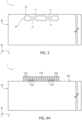
- Figure 3 illustrates, according to a further embodiment, the semiconductor body 30 including the membrane 10 and the cavity 20, wherein the cavity 20 accommodated therein a plurality of bumps 11 (at the top side 20a) and a plurality of bumps 12 (at the bottom side 20b).
- the bumps 11 and 12 are formed as described with reference to Figures 2A-2E .
- Figures 4A-4E illustrate a method for manufacturing the wafer 1 of Figure 1 , in particular for forming the bumps 11, 12, according to an alternative embodiment with respect to that of Figures 2A-2E .
- this may be diced to isolate a plurality of dies or chips manufactured simultaneously as described herein.
- the wafer 1 comprises the semiconductor body 30 (possibly previously processed, as needed, for example including a monocrystalline silicon epitaxial layer grown on a monocrystalline silicon substrate).
- the view of Figure 4A is along section line IV-IV of Figure 4B .
- a photoresist mask 52 is provided above the top surface 30a of the semiconductor body 30 by a photolithography step.
- the mask 52 is formed at regions of the semiconductor body 30 wherein it is desired to form the buried cavity 20 and, consequently, the membrane 10 suspended thereon.
- the mask 52 defines a honeycomb lattice, having mask regions 52a for example of hexagonal shape, close to each other and separated from each other by through openings 52c extending through the entire thickness of the mask 52.
- a second mask region 52b has no through openings 52c.
- first and the second mask regions 52a, 52b are regions wherein the photoresist material is physically present ("full” regions); the through openings 52c are regions wherein the photoresist material has been removed (“empty” regions) by the photolithographic process, having the top surface 30a of the semiconductor body 30 exposed therethrough.
- the first mask regions 52a have, in top view, a first value of base area; the second mask region 52b has, in top view, a second value of base area, greater than the first value of base area.
- the portion of the mask 52 wherein the first mask regions 52a are present has a full/empty ratio of the type already described for the portion 36 of the mask 52 of Figure 2A or 2B .
- the portion of the mask 52 wherein the second mask region 52b is present has no empty spaces.
- the first mask regions 52a have a hexagonal shape and diameter (both along the X and Y axis) in the range 1.8-2.1 ⁇ m, and are separated from each other by a gap 32c having extension (both along the X and Y axis) in the range 0.9-1.2 ⁇ m.
- the second mask region 52b has any shape (e.g. generically polygonal), chosen during the design step, for example of the type illustrated in Figures 5A-5C according to the respective embodiments.
- an etching of the semiconductor body 30 is performed, forming trenches 58 having depths, along the Z axis, of a few micrometers, for example depth comprised between 0.5 ⁇ m and 50 pm.
- the trenches 58 define columns 62a, 62b of silicon having a shape corresponding to the shape of the regions 52a, 52b defined by the mask 52.
- silicon columns 62a are formed which have shape, dimensions and mutual distance uniform to each other, as determined by the first mask region 52a; similarly, a single silicon column 62b is formed, contiguous to the silicon columns 62a (in particular, surrounded by the silicon columns 62a, at a distance determined by the trenches 58), which has a shape and dimensions defined by the second mask region 52b.
- Each column 62a has, for example, a hexagonal shape with a diameter equal to about 2 ⁇ m, and is separated from an adjacent column 62a, along X and along Y, by about 1 ⁇ m.
- diameter and spacing of the columns 62a are designed of such a value as to allow a top closure of the trenches 58 during the epitaxial growth step described with reference to Figure 4D .
- the mask 52 is removed.
- an epitaxial growth is performed in a deoxidizing environment (typically, in an atmosphere having a high concentration of hydrogen, preferably using trichlorosilane-SiHCl 3 ).
- the epitaxial growth is performed at least until the trenches 58 are closed upwardly (for example, for 45 seconds at a temperature close to 1200°C).
- an epitaxial layer 70 grows above the silicon columns 62a, 62b, closes the trenches 58 upwardly and traps therein the gas present (here, molecules of hydrogen H 2 ) .
- An annealing step is then performed, for example for about 30-40 minutes at a temperature of about 1190-1200°C.
- the annealing step causes, Figure 4E , a migration of the silicon atoms which tend to move to the lower energy position, in a per se known manner, as for example discussed in the article by T. Sato, N. Aoki, I. Mizushima and Y. Tsunashima, "A New Substrate Engineering for the Formation of Empty Space in Silicon (ESS) Induced by Silicon Surface Migration", IEDM 1999, pp. 517-520 .
- the silicon atoms migrate and form the cavity 20 closed upwardly by the epitaxial layer 70 (which, now, forms the membrane 10).
- the annealing is performed in an H 2 atmosphere so as to prevent the hydrogen present in the trenches 58 from escaping through the epitaxial layer towards the outside and to increase the concentration of hydrogen present in the cavity 20 if that trapped during the epitaxial growth step were not sufficient.
- the annealing may be carried out in a nitrogen environment.
- forming the buried cavity 20 comprises concurrently forming different types of cavities, or sub-cavities, joined to each other and in mutual connection.
- a first type of sub-cavity 74 is formed at the silicon column 62b, and a second type of sub-cavity 75 is formed at the silicon columns 62a.
- the sub-cavity 74 of the first type has a maximum extension, along the Z axis, lower than the maximum extension, along the Z axis, of the second type of sub-cavity 75.
- the typological division among the sub-cavities of different type is qualitative and not clear-cut.
- the bumps 11, 12 are formed at the sub-cavity 74 of the first type and tend to partially occlude, or locally narrow, the buried cavity 20.
- Figure 4E illustrates, for simplicity of representation, bumps 11, 12 having the same thickness along the Z axis
- the advantageous effect of the present invention would be obtained even if (by variation in the process parameters) one of the bumps 11, 12 protruded from the respective side for a maximum thickness, along Z, greater than the corresponding maximum thickness of the other bump 11, 12.
- one of the bumps 11 and 12 might be absent.
- Figure 5A illustrates, in XY plane view, a layout of the column, or pillar, 62b.
- the column 62b has the shape of a four-pointed "star” or of a "cross”, of maximum dimension (from tip to tip), along X and along Y equal to a few micrometers, for example 7 ⁇ m along the X axis and 5 ⁇ m along the Y axis.
- Figure 5B illustrates, in XY plane view, a further layout of the column, or pillar, 62b.
- the column 62b has the shape of a six-pointed "star", and for example maximum dimension (from tip to tip), along Y equal for example to 8 ⁇ m and minimum dimension, along X, equal for example to 6 ⁇ m.
- Figure 5C illustrates, in XY plane view, a further layout of the column, or pillar, 62b.
- the column 62b has the shape of a twelve-pointed "star” or “flower”, and the maximum dimension (from tip to tip), along X or along Y, comprised for example between 12 and 14 ⁇ m.
- Figures 6A-6G illustrate a manufacturing method of the wafer 1, in particular of the membrane 10 suspended on the buried cavity 20 which includes at least the bump 11, according to a further embodiment of the present invention.
- the wafer 1 may be diced to isolate a plurality of dies or chips manufactured simultaneously as described herein.
- the wafer 1 comprises the semiconductor body 30, here of monocrystalline silicon.
- a photoresist mask 83 is provided above the top surface 30a of the semiconductor body 30 by a photolithography step. The mask 83 is formed at regions of the semiconductor body 30 wherein it is desired to form the cavity 20.
- the mask 83 defines a honeycomb lattice, having mask regions, for example of a hexagonal shape, close to each other.
- each column 87 has a diameter equal to about 1 ⁇ m and is separated from an adjacent column, along X or along Y, by about 1 ⁇ m. In general, diameter and spacing of the columns 87 are chosen of such a value as to allow a top closure of the trenches 86 during the epitaxial growth step described hereinbelow.
- the mask 83 is removed and an epitaxial growth is performed in a deoxidizing environment (typically, in an atmosphere having a high concentration of hydrogen, preferably using trichlorosilane-SiHCls).
- the epitaxial growth is performed at least until the trenches 86 are closed upwardly (for example, for 45 seconds at a temperature close to 1200°C).
- a sealing layer 88 (hereinafter forming, at least in part, the membrane 10), is grown epitaxially above the silicon columns 87; the sealing layer 88 closes the trenches 86 upwardly and traps therein the gas present (here, molecules of hydrogen H 2 ) .
- An annealing step is then performed, for example for about 30-40 minutes at a temperature of about 1190-1200°C.
- the annealing step causes, Figure 6E , a migration of the silicon atoms which tend to move to the lower energy position, in a per se known manner, as for example discussed in the article by T. Sato, N. Aoki, I. Mizushima and Y. Tsunashima, "A New Substrate Engineering for the Formation of Empty Space in Silicon (ESS) Induced by Silicon Surface Migration", IEDM 1999, pp. 517-520 .
- the silicon atoms migrate completely and form the cavity 20, closed upwardly by the sealing layer 88, of Silicon.
- the annealing is performed in an H 2 atmosphere so as to prevent the hydrogen present in the trenches 86 from escaping through the epitaxial layer towards the outside and to increase the concentration of hydrogen present in the cavity 20 if that trapped during the epitaxial growth step were not sufficient.
- the annealing may be carried out in a nitrogen environment.
- the sealing layer 88 is selectively removed at a portion thereof wherein the bump 11 is intended to be formed.
- a chemical etching (arrows 90 in Figure 6F ) is performed using an etching mask 92 to form an opening 89 passing through the entire thickness of the sealing layer 88.
- the through opening 89 reaches the cavity 20, putting it in connection with the external environment.
- the through opening 89 has, for example, a circular or generically polygonal shape in XY plane view, for example with a diameter comprised between 0.1 and 5 ⁇ m, more particularly between 0.1 and 1 ⁇ m, even more particularly between 0.1 and 0.3 ⁇ m.
- the through opening 89 may also have irregular shapes, or for example one of the shapes and dimensions illustrated in Figures 5A-5C for the element 62b.
- an epitaxial growth step is performed at the sealing layer 88, such that it closes the through opening 89 thus isolating the cavity 20 from the external environment.
- the Silicon also grows epitaxially towards the inside of the cavity 20, at the through opening 89, forming a protuberance that extends towards the inside of the cavity 20.
- the through opening 89 closes and this protuberance forms the bump 11.
- the cavity 20, at the end of the method is buried in the semiconductor body 30 and its internal pressure is defined by the pressure present in the reaction chamber during the epitaxial growth leading to the formation of the bump 11.
- the membrane 10 may be thinned, if necessary, for example by CMP technique.
- Figures 7A-7C illustrate a further technical solution for manufacturing a buried cavity provided with one or more bumps.
- Figures 7A-7C are illustrated in a triaxial reference system of X, Y, Z axes orthogonal to each other. Reference will be made hereinafter to the processing of wafers; however, what has been described applies similarly to the processing of portions of a semiconductor wafer, for example dies. Similarly, at the end of the processing steps of the wafers, these may be diced ("dicing" operation) to isolate a plurality of dies or chips manufactured simultaneously as described herein.
- a first wafer 100 of semiconductor material for example of Silicon, is shaped so as to form, at one front side 100a thereof, a recess 102 having a bottom side 102a.
- the bottom side 102a has a protuberance, or bump, 104, for example having a circular, polygonal or irregular shape, which extends moving away from the bottom side 102a.
- the bump 104 may have one of the shapes described and illustrated with reference to Figures 5A-5C for the element 62b.
- the bump 104 extends, from the bottom side 102a, for a height, along the Z axis, comprised between 0.01 and 1 ⁇ m (in particular between 0.1 and 1 ⁇ m).
- a second wafer 110 of semiconductor material is arranged, having a front side 112a and a rear side 110b opposite to each other along the Z axis.
- the second wafer 110 is for example of Silicon.
- the second wafer 110 is shaped so as to form, at the front side 112a, a recess 112 having a bottom side 112a.
- the bottom side 112a has a protuberance, or bump, 114, for example having a circular, polygonal or irregular shape.
- the bump 114 may have one of the shapes described and illustrated with reference to Figures 5A-5C for the element 62b.
- the bump 114 extends, from the bottom side 112a, for a height, along the Z axis, comprised between 0.01 and 1 ⁇ m (in particular between 0.1 and 1 pm).
- the bumps 104 and 114 are formed in such a way that, when the first and the second wafers 100, 110 are coupled to each other as described with reference to Figure 7C , the bumps 104 and 114 are at least partially aligned with each other along the direction of the Z axis.
- the first wafer 100 and the second wafer 110 are coupled to each other at coupling regions 108 extending laterally to (i.e., surrounding) the recesses 102, 112.
- the coupling may be carried out by per se known wafer- to-wafer bonding techniques. For example, it is possible to use glue, double-sided adhesive layers, glass frit, etc.
- the coupling between the wafers 100, 110 is performed in such a way that the recesses 102, 112 form, together, a cavity 120 fluidically isolated from the external environment.
- the second wafer 110 thus forms, at its rear side 110b, a membrane 121 suspended on the cavity 120. It is possible to thin the second wafer 110 at the rear side 110b to obtain a desired thickness for the membrane 121.
- the membrane 121 is for bending when a suitable external force F is applied along the Z direction as identified by arrow 124. At rest, when no external force F acts on the membrane 121, the membrane 121 is substantially parallel to the XY plane. In the presence of a suitable force F, the membrane 121 bends, and, as the force F increases, the membrane 121 bends up to a maximum bending point wherein the bumps 104, 114 are in mutual contact.
- the bumps 104, 114 operate, in this context, as antistiction structures, minimizing the risk of irreversible stiction between the opposite sides 102a, 112a internal to the cavity 120 when, during use, the opposite sides 102a, 112a come close to each other.
- the contact occurs exclusively between the bumps 104, 114 which have a reduced contact surface and, therefore, also the stiction forces are consequently reduced.
- the second wafer 110 is shaped so as not to have the bump 114.
- the cavity 120 accommodates the sole bump 104.
- one of or both the first and the second wafers 100, 110 may be shaped so as to have a plurality of bumps 104 and/or a plurality of bumps 114, with shapes and dimensions equal to or different from each other.
- the present invention may find application as a pressure sensor (in particular of differential type), or as a fluidic micro-valve or fluidic micro-pump with an actuation that is, in particular, piezoelectric.
- the transduction of the signal applied on the membrane 10, 110 may occur according to any of the known techniques, for example by forming piezoresistors on the membrane 10, 110, or in proximity thereto, in a manner known per se and not an object of the present invention.
- the piezoresistive elements have P-type conductivity and the membrane has N-type conductivity (the electrical conductivities are obtained by implanting dopant species, in a per se known manner).
- the piezoresistors may be made of polysilicon above the membrane.
- FIG. 7A-7C , or 8A-8B is suitable for manufacturing a capacitive pressure sensor, using coupling regions 108 which electrically insulate the two wafers 100, 110 which form the two electrons, or plates, of a capacitor.
- a pressure on the membrane 121 it deflects, reducing its distance from the bottom electrode (wafer 100).
- the capacitance of the sensing capacitor increases.
- an indication of the applied pressure force F
- the present invention allows antistiction structures to be provided inside a buried cavity, maintaining a desired pressure (defined during the design step) of the cavity.
- the cavity has an internal pressure lower than the atmospheric pressure wherein the structure thus formed is designed to operate.
- the layout of the buried cavity 20, 120 may be freely designed according to parameters that are not an object of the present invention.
- the buried cavity 20, 120 may have, in XY plane plan view, a shape chosen from quadrangular, circular, quadrangular with rounded edges, polygonal, irregular.
- hexagonal or honeycomb shape of the base area 8 (in XY plane view) of the columnar structures 42a, 42b may be different, i.e. generically polygonal or circular.
- the shape of the columnar structures 42a, 42b may further vary; for example they may be replaced by septa of semiconductor material, or in general by other thin structures capable of allowing the migration of silicon during the annealing step, favoring or allowing the formation of the buried cavity.
Landscapes
- Engineering & Computer Science (AREA)
- Microelectronics & Electronic Packaging (AREA)
- Manufacturing & Machinery (AREA)
- Computer Hardware Design (AREA)
- Chemical & Material Sciences (AREA)
- Analytical Chemistry (AREA)
- Pressure Sensors (AREA)
Applications Claiming Priority (1)
| Application Number | Priority Date | Filing Date | Title |
|---|---|---|---|
| IT102022000008822A IT202200008822A1 (it) | 2022-05-02 | 2022-05-02 | Struttura mems includente una cavita' sepolta con protuberanze antiadesione, e relativi procedimenti di fabbricazione |
Publications (1)
| Publication Number | Publication Date |
|---|---|
| EP4273091A1 true EP4273091A1 (de) | 2023-11-08 |
Family
ID=82308260
Family Applications (1)
| Application Number | Title | Priority Date | Filing Date |
|---|---|---|---|
| EP23167983.8A Pending EP4273091A1 (de) | 2022-05-02 | 2023-04-14 | Mems-struktur mit einem vergrabenen hohlraum mit antihaftungsvorsprüngen und herstellungsverfahren dafür |
Country Status (4)
| Country | Link |
|---|---|
| US (1) | US20230348258A1 (de) |
| EP (1) | EP4273091A1 (de) |
| CN (2) | CN220766508U (de) |
| IT (1) | IT202200008822A1 (de) |
Citations (4)
| Publication number | Priority date | Publication date | Assignee | Title |
|---|---|---|---|---|
| US20050181529A1 (en) | 2003-12-16 | 2005-08-18 | Hubert Benzel | Method for manufacturing a semiconductor component, as well as a semiconductor component, in particular a membrane sensor |
| EP2075224A2 (de) | 2007-12-27 | 2009-07-01 | Commissariat a L'Energie Atomique | Verfahren zur Herstellung eines mikomechanischen oder nanomechanischen Elements mit Anti-Haft-Anschlägen |
| EP3845485A1 (de) | 2018-08-28 | 2021-07-07 | CSMC Technologies Fab2 Co., Ltd. | Temperatursensorherstellungsverfahren und temperatursensor |
| US20210285983A1 (en) | 2020-02-28 | 2021-09-16 | Seiko Epson Corporation | Physical quantity sensor, electronic apparatus, and vehicle |
-
2022
- 2022-05-02 IT IT102022000008822A patent/IT202200008822A1/it unknown
-
2023
- 2023-04-14 EP EP23167983.8A patent/EP4273091A1/de active Pending
- 2023-04-18 US US18/302,610 patent/US20230348258A1/en active Pending
- 2023-04-28 CN CN202321015454.7U patent/CN220766508U/zh active Active
- 2023-04-28 CN CN202310480979.6A patent/CN116986549A/zh active Pending
Patent Citations (4)
| Publication number | Priority date | Publication date | Assignee | Title |
|---|---|---|---|---|
| US20050181529A1 (en) | 2003-12-16 | 2005-08-18 | Hubert Benzel | Method for manufacturing a semiconductor component, as well as a semiconductor component, in particular a membrane sensor |
| EP2075224A2 (de) | 2007-12-27 | 2009-07-01 | Commissariat a L'Energie Atomique | Verfahren zur Herstellung eines mikomechanischen oder nanomechanischen Elements mit Anti-Haft-Anschlägen |
| EP3845485A1 (de) | 2018-08-28 | 2021-07-07 | CSMC Technologies Fab2 Co., Ltd. | Temperatursensorherstellungsverfahren und temperatursensor |
| US20210285983A1 (en) | 2020-02-28 | 2021-09-16 | Seiko Epson Corporation | Physical quantity sensor, electronic apparatus, and vehicle |
Non-Patent Citations (1)
| Title |
|---|
| T. SATON. AOKII. MIZUSHIMAY. TSUNASHIMA: "A New Substrate Engineering for the Formation of Empty Space in Silicon (ESS) Induced by Silicon Surface Migration", IEDM, 1999, pages 517 - 520 |
Also Published As
| Publication number | Publication date |
|---|---|
| US20230348258A1 (en) | 2023-11-02 |
| IT202200008822A1 (it) | 2023-11-02 |
| CN220766508U (zh) | 2024-04-12 |
| CN116986549A (zh) | 2023-11-03 |
Similar Documents
| Publication | Publication Date | Title |
|---|---|---|
| CN102401706B (zh) | Mems压力传感器件及其制造方法 | |
| US6816301B1 (en) | Micro-electromechanical devices and methods of manufacture | |
| US7502482B2 (en) | Membrane and method for the production of the same | |
| US6973835B2 (en) | Pressure sensor | |
| EP2014612B1 (de) | Verfahren zur Herstellung einer mikroelektromechanischen Systemvorrichtung unter Vermeidung einer Opferschicht | |
| US20150192487A1 (en) | Low pressure sensors and flow sensors | |
| EP3052901B1 (de) | Trägheits- und drucksensoren auf einem einzelnen chip | |
| US20150276533A1 (en) | Low Pressure Sensor and Flow Sensor | |
| US8426931B2 (en) | Semiconductor device and method of fabricating the semiconductor device | |
| US20110221014A1 (en) | Pressure sensor and method for manufacturing the pressure sensor | |
| US11573137B2 (en) | Surface stress sensor, hollow structural element, and method for manufacturing same | |
| US20230126952A1 (en) | Surface stress sensor, hollow structural element, and method for manufacturing same | |
| US10954120B2 (en) | Micromechanical sensor that includes a stress decoupling structure | |
| US10183862B2 (en) | Method of strain gauge fabrication using a transfer substrate | |
| WO2017148847A1 (en) | Mems device using a released device layer as membrane | |
| WO2016119417A1 (zh) | 一种加速度计的z轴结构及其生产方法 | |
| WO2020177339A1 (zh) | 压力传感器及其制造方法 | |
| EP4273091A1 (de) | Mems-struktur mit einem vergrabenen hohlraum mit antihaftungsvorsprüngen und herstellungsverfahren dafür | |
| JP6305647B2 (ja) | 電気機械デバイスを製造するための方法及び対応するデバイス | |
| US10585074B2 (en) | Method of fabricating a MEMS and/or NEMS structure comprising at least two elements suspended from a support at different distances from said support | |
| CN107764459B (zh) | 压力传感器以及其制造方法 | |
| US20020104379A1 (en) | Accelerometer with re-entrant grooves | |
| EP1196349A1 (de) | Mikroelektromechanische bauelemente und verfahren zu deren herstellung | |
| CN210559358U (zh) | 压力传感器 | |
| US10472227B2 (en) | Micro-device having a plurality of mobile elements arranged in a plurality of embedded cavities |
Legal Events
| Date | Code | Title | Description |
|---|---|---|---|
| PUAI | Public reference made under article 153(3) epc to a published international application that has entered the european phase |
Free format text: ORIGINAL CODE: 0009012 |
|
| STAA | Information on the status of an ep patent application or granted ep patent |
Free format text: STATUS: THE APPLICATION HAS BEEN PUBLISHED |
|
| AK | Designated contracting states |
Kind code of ref document: A1 Designated state(s): AL AT BE BG CH CY CZ DE DK EE ES FI FR GB GR HR HU IE IS IT LI LT LU LV MC ME MK MT NL NO PL PT RO RS SE SI SK SM TR |
|
| STAA | Information on the status of an ep patent application or granted ep patent |
Free format text: STATUS: REQUEST FOR EXAMINATION WAS MADE |
|
| 17P | Request for examination filed |
Effective date: 20240412 |
|
| RBV | Designated contracting states (corrected) |
Designated state(s): AL AT BE BG CH CY CZ DE DK EE ES FI FR GB GR HR HU IE IS IT LI LT LU LV MC ME MK MT NL NO PL PT RO RS SE SI SK SM TR |