EP4273091A1 - Mems structure including a buried cavity with antistiction protuberances, and manufacturing methods thereof - Google Patents
Mems structure including a buried cavity with antistiction protuberances, and manufacturing methods thereof Download PDFInfo
- Publication number
- EP4273091A1 EP4273091A1 EP23167983.8A EP23167983A EP4273091A1 EP 4273091 A1 EP4273091 A1 EP 4273091A1 EP 23167983 A EP23167983 A EP 23167983A EP 4273091 A1 EP4273091 A1 EP 4273091A1
- Authority
- EP
- European Patent Office
- Prior art keywords
- bump
- antistiction
- cavity
- along
- anyone
- Prior art date
- Legal status (The legal status is an assumption and is not a legal conclusion. Google has not performed a legal analysis and makes no representation as to the accuracy of the status listed.)
- Pending
Links
Images





Classifications
-
- B—PERFORMING OPERATIONS; TRANSPORTING
- B81—MICROSTRUCTURAL TECHNOLOGY
- B81B—MICROSTRUCTURAL DEVICES OR SYSTEMS, e.g. MICROMECHANICAL DEVICES
- B81B3/00—Devices comprising flexible or deformable elements, e.g. comprising elastic tongues or membranes
- B81B3/0002—Arrangements for avoiding sticking of the flexible or moving parts
- B81B3/001—Structures having a reduced contact area, e.g. with bumps or with a textured surface
-
- B—PERFORMING OPERATIONS; TRANSPORTING
- B81—MICROSTRUCTURAL TECHNOLOGY
- B81B—MICROSTRUCTURAL DEVICES OR SYSTEMS, e.g. MICROMECHANICAL DEVICES
- B81B7/00—Microstructural systems ; Auxiliary parts of microstructural devices or systems
- B81B7/02—Microstructural systems ; Auxiliary parts of microstructural devices or systems containing distinct electrical or optical devices of particular relevance for their function, e.g. microelectro-mechanical systems [MEMS]
-
- B—PERFORMING OPERATIONS; TRANSPORTING
- B81—MICROSTRUCTURAL TECHNOLOGY
- B81B—MICROSTRUCTURAL DEVICES OR SYSTEMS, e.g. MICROMECHANICAL DEVICES
- B81B7/00—Microstructural systems ; Auxiliary parts of microstructural devices or systems
- B81B7/0032—Packages or encapsulation
- B81B7/0035—Packages or encapsulation for maintaining a controlled atmosphere inside of the chamber containing the MEMS
-
- B—PERFORMING OPERATIONS; TRANSPORTING
- B81—MICROSTRUCTURAL TECHNOLOGY
- B81B—MICROSTRUCTURAL DEVICES OR SYSTEMS, e.g. MICROMECHANICAL DEVICES
- B81B7/00—Microstructural systems ; Auxiliary parts of microstructural devices or systems
- B81B7/0032—Packages or encapsulation
- B81B7/0045—Packages or encapsulation for reducing stress inside of the package structure
-
- B—PERFORMING OPERATIONS; TRANSPORTING
- B81—MICROSTRUCTURAL TECHNOLOGY
- B81C—PROCESSES OR APPARATUS SPECIALLY ADAPTED FOR THE MANUFACTURE OR TREATMENT OF MICROSTRUCTURAL DEVICES OR SYSTEMS
- B81C1/00—Manufacture or treatment of devices or systems in or on a substrate
- B81C1/00015—Manufacture or treatment of devices or systems in or on a substrate for manufacturing microsystems
- B81C1/00023—Manufacture or treatment of devices or systems in or on a substrate for manufacturing microsystems without movable or flexible elements
- B81C1/00047—Cavities
-
- B—PERFORMING OPERATIONS; TRANSPORTING
- B81—MICROSTRUCTURAL TECHNOLOGY
- B81C—PROCESSES OR APPARATUS SPECIALLY ADAPTED FOR THE MANUFACTURE OR TREATMENT OF MICROSTRUCTURAL DEVICES OR SYSTEMS
- B81C1/00—Manufacture or treatment of devices or systems in or on a substrate
- B81C1/00015—Manufacture or treatment of devices or systems in or on a substrate for manufacturing microsystems
- B81C1/00134—Manufacture or treatment of devices or systems in or on a substrate for manufacturing microsystems comprising flexible or deformable structures
- B81C1/00158—Diaphragms, membranes
-
- B—PERFORMING OPERATIONS; TRANSPORTING
- B81—MICROSTRUCTURAL TECHNOLOGY
- B81C—PROCESSES OR APPARATUS SPECIALLY ADAPTED FOR THE MANUFACTURE OR TREATMENT OF MICROSTRUCTURAL DEVICES OR SYSTEMS
- B81C1/00—Manufacture or treatment of devices or systems in or on a substrate
- B81C1/00015—Manufacture or treatment of devices or systems in or on a substrate for manufacturing microsystems
- B81C1/00261—Processes for packaging MEMS devices
- B81C1/00277—Processes for packaging MEMS devices for maintaining a controlled atmosphere inside of the cavity containing the MEMS
-
- B—PERFORMING OPERATIONS; TRANSPORTING
- B81—MICROSTRUCTURAL TECHNOLOGY
- B81C—PROCESSES OR APPARATUS SPECIALLY ADAPTED FOR THE MANUFACTURE OR TREATMENT OF MICROSTRUCTURAL DEVICES OR SYSTEMS
- B81C1/00—Manufacture or treatment of devices or systems in or on a substrate
- B81C1/00015—Manufacture or treatment of devices or systems in or on a substrate for manufacturing microsystems
- B81C1/00261—Processes for packaging MEMS devices
- B81C1/00301—Connecting electric signal lines from the MEMS device with external electrical signal lines, e.g. through vias
-
- B—PERFORMING OPERATIONS; TRANSPORTING
- B81—MICROSTRUCTURAL TECHNOLOGY
- B81B—MICROSTRUCTURAL DEVICES OR SYSTEMS, e.g. MICROMECHANICAL DEVICES
- B81B2201/00—Specific applications of microelectromechanical systems
- B81B2201/02—Sensors
- B81B2201/0264—Pressure sensors
-
- B—PERFORMING OPERATIONS; TRANSPORTING
- B81—MICROSTRUCTURAL TECHNOLOGY
- B81B—MICROSTRUCTURAL DEVICES OR SYSTEMS, e.g. MICROMECHANICAL DEVICES
- B81B2203/00—Basic microelectromechanical structures
- B81B2203/01—Suspended structures, i.e. structures allowing a movement
- B81B2203/0127—Diaphragms, i.e. structures separating two media that can control the passage from one medium to another; Membranes, i.e. diaphragms with filtering function
-
- B—PERFORMING OPERATIONS; TRANSPORTING
- B81—MICROSTRUCTURAL TECHNOLOGY
- B81B—MICROSTRUCTURAL DEVICES OR SYSTEMS, e.g. MICROMECHANICAL DEVICES
- B81B2203/00—Basic microelectromechanical structures
- B81B2203/03—Static structures
- B81B2203/0315—Cavities
-
- B—PERFORMING OPERATIONS; TRANSPORTING
- B81—MICROSTRUCTURAL TECHNOLOGY
- B81B—MICROSTRUCTURAL DEVICES OR SYSTEMS, e.g. MICROMECHANICAL DEVICES
- B81B2203/00—Basic microelectromechanical structures
- B81B2203/03—Static structures
- B81B2203/0323—Grooves
- B81B2203/033—Trenches
-
- B—PERFORMING OPERATIONS; TRANSPORTING
- B81—MICROSTRUCTURAL TECHNOLOGY
- B81B—MICROSTRUCTURAL DEVICES OR SYSTEMS, e.g. MICROMECHANICAL DEVICES
- B81B2203/00—Basic microelectromechanical structures
- B81B2203/03—Static structures
- B81B2203/0361—Tips, pillars
-
- B—PERFORMING OPERATIONS; TRANSPORTING
- B81—MICROSTRUCTURAL TECHNOLOGY
- B81B—MICROSTRUCTURAL DEVICES OR SYSTEMS, e.g. MICROMECHANICAL DEVICES
- B81B2207/00—Microstructural systems or auxiliary parts thereof
- B81B2207/09—Packages
- B81B2207/091—Arrangements for connecting external electrical signals to mechanical structures inside the package
-
- B—PERFORMING OPERATIONS; TRANSPORTING
- B81—MICROSTRUCTURAL TECHNOLOGY
- B81B—MICROSTRUCTURAL DEVICES OR SYSTEMS, e.g. MICROMECHANICAL DEVICES
- B81B2207/00—Microstructural systems or auxiliary parts thereof
- B81B2207/11—Structural features, others than packages, for protecting a device against environmental influences
-
- B—PERFORMING OPERATIONS; TRANSPORTING
- B81—MICROSTRUCTURAL TECHNOLOGY
- B81C—PROCESSES OR APPARATUS SPECIALLY ADAPTED FOR THE MANUFACTURE OR TREATMENT OF MICROSTRUCTURAL DEVICES OR SYSTEMS
- B81C2201/00—Manufacture or treatment of microstructural devices or systems
- B81C2201/01—Manufacture or treatment of microstructural devices or systems in or on a substrate
- B81C2201/0101—Shaping material; Structuring the bulk substrate or layers on the substrate; Film patterning
- B81C2201/0111—Bulk micromachining
- B81C2201/0116—Thermal treatment for structural rearrangement of substrate atoms, e.g. for making buried cavities
-
- B—PERFORMING OPERATIONS; TRANSPORTING
- B81—MICROSTRUCTURAL TECHNOLOGY
- B81C—PROCESSES OR APPARATUS SPECIALLY ADAPTED FOR THE MANUFACTURE OR TREATMENT OF MICROSTRUCTURAL DEVICES OR SYSTEMS
- B81C2201/00—Manufacture or treatment of microstructural devices or systems
- B81C2201/01—Manufacture or treatment of microstructural devices or systems in or on a substrate
- B81C2201/0101—Shaping material; Structuring the bulk substrate or layers on the substrate; Film patterning
- B81C2201/0128—Processes for removing material
- B81C2201/013—Etching
- B81C2201/0135—Controlling etch progression
- B81C2201/014—Controlling etch progression by depositing an etch stop layer, e.g. silicon nitride, silicon oxide, metal
-
- B—PERFORMING OPERATIONS; TRANSPORTING
- B81—MICROSTRUCTURAL TECHNOLOGY
- B81C—PROCESSES OR APPARATUS SPECIALLY ADAPTED FOR THE MANUFACTURE OR TREATMENT OF MICROSTRUCTURAL DEVICES OR SYSTEMS
- B81C2201/00—Manufacture or treatment of microstructural devices or systems
- B81C2201/01—Manufacture or treatment of microstructural devices or systems in or on a substrate
- B81C2201/0101—Shaping material; Structuring the bulk substrate or layers on the substrate; Film patterning
- B81C2201/0156—Lithographic techniques
-
- B—PERFORMING OPERATIONS; TRANSPORTING
- B81—MICROSTRUCTURAL TECHNOLOGY
- B81C—PROCESSES OR APPARATUS SPECIALLY ADAPTED FOR THE MANUFACTURE OR TREATMENT OF MICROSTRUCTURAL DEVICES OR SYSTEMS
- B81C2201/00—Manufacture or treatment of microstructural devices or systems
- B81C2201/01—Manufacture or treatment of microstructural devices or systems in or on a substrate
- B81C2201/0161—Controlling physical properties of the material
- B81C2201/0163—Controlling internal stress of deposited layers
- B81C2201/0169—Controlling internal stress of deposited layers by post-annealing
-
- B—PERFORMING OPERATIONS; TRANSPORTING
- B81—MICROSTRUCTURAL TECHNOLOGY
- B81C—PROCESSES OR APPARATUS SPECIALLY ADAPTED FOR THE MANUFACTURE OR TREATMENT OF MICROSTRUCTURAL DEVICES OR SYSTEMS
- B81C2201/00—Manufacture or treatment of microstructural devices or systems
- B81C2201/01—Manufacture or treatment of microstructural devices or systems in or on a substrate
- B81C2201/0174—Manufacture or treatment of microstructural devices or systems in or on a substrate for making multi-layered devices, film deposition or growing
- B81C2201/0176—Chemical vapour Deposition
- B81C2201/0177—Epitaxy, i.e. homo-epitaxy, hetero-epitaxy, GaAs-epitaxy
Definitions
- the present disclosure relates to a micromechanical or microelectromechanical structure, to manufacturing methods thereof, and to a MEMS transducer; in particular, this structure includes a buried cavity having one or more antistiction bumps extending therein.
- integrated pressure sensors may be provided with micromanufacturing techniques. These sensors typically comprise a thin membrane, or diaphragm, suspended above a cavity obtained in a semiconductor body. Piezoresistive elements connected to each other are formed within the membrane and connected in a Wheatstone bridge. When subject to a pressure, the membrane undergoes a deformation, causing a variation in the resistance of the piezoresistive elements, and therefore an imbalance of the Wheatstone bridge.
- capacitive sensors are available, wherein the membrane provides a first plate of a capacitor, while a second plate is provided by a fixed reference. In use, the deflection of the membrane generates a variation in the capacitance of the capacitor, which may be detected and associated with the pressure exerted on the membrane.
- the stiction phenomenon is typically generated by the surface forces that are exerted between the surfaces of two bodies coming into contact. Of course, the wider the contact zone, the greater the interaction force between the surfaces.
- further factors that are to be considered in assessing and preventing stiction are, inter alia, the roughness of the surfaces, their wear, the level of humidity and the temperature of the environment wherein the micromechanical structures operate. These parameters are particularly difficult to monitor in case of membranes suspended on buried cavities, due to the inherent difficulty of operating internally to these buried cavities to reduce the causes of stiction.
- the membrane is formed by an epitaxial growth.
- the increase in the epitaxial growth time, necessary to obtain a thicker membrane, has several drawbacks such as, for example, an increase in costs and an increase in the non-uniformity of the rear side of the semiconductor wafer, which cause difficulties in handling the wafer and incompatibility problems with subsequent steps of the manufacturing process.
- the known integrated semiconductor pressure sensors are typically designed and used to measure relatively low pressures (for example up to 0.1 MPa), and a stiffening of the membrane thereof might cause an operating difficulty at such pressures.
- EP2075224 relates to the field of micromechanical and/or nanomechanical devices comprising mobile elements, and more particularly that of microelectromechanical systems (MEMS) and/or nanoelectromechanical systems (NEMS) comprising mobile elements capable of coming into contact with other elements of the MEMS and/or NEMS during its operation.
- MEMS microelectromechanical systems
- NEMS nanoelectromechanical systems
- US 2021/285983 relates to a physical quantity sensor, an electronic apparatus, and a vehicle.
- US 2005/181529 relates to a method for manufacturing a semiconductor component.
- EP3845485 relates to the field of temperature sensor, and in particular to a manufacturing method for a temperature sensor, and a temperature sensor.
- the aim of the present invention is to provide a structure, manufacturing methods thereof, and a microelectromechanical transducer, for overcoming the drawbacks of the prior art.
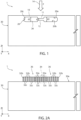
- Figure 1 illustrates, in a triaxial system of X, Y, Z axes orthogonal to each other, a portion of a semiconductor wafer 1 including a micromechanical or microelectromechanical (MEMS) structure according to an embodiment of the present invention.
- MEMS microelectromechanical
- the wafer 1, or die comprises a semiconductor body 30 which accommodates a membrane 10 suspended on a cavity 20 buried in the semiconductor body 30.
- the cavity 20 is delimited upwardly by a top side (or wall) 20a (which is part of the membrane 10) and downwardly by a bottom side (or wall) 20b (which is part of the semiconductor body 30), opposite to the top side 20a along the Z axis.
- Lateral sides (or walls) 20c physically connect the top side 20a with the bottom side 20b.
- the membrane 10 extends, at rest, substantially parallel to the XY plane. It is however possible to design the membrane 10 having internal stresses such that the membrane 10 extends, at rest, not perfectly parallel to the XY plane, but with a concave or convex shape. In the following of the present description and in the Figures it is assumed, for simplicity of description and representation, that the membrane 10 is parallel to the XY plane.
- the cavity 20 has one or more protrusions, or protuberances, or “bumps", 11 which extend from the top side 20a towards the bottom side 20b, and vice versa, one or more protrusions, or protuberances, or “bumps", 12 which extend from the bottom side 20b towards the top side 20a.
- Figure 1 illustrates a single bump 11 and a single bump 12.
- one of the bump 11 and the bump 12 may be omitted.
- the membrane 10 is therefore partially suspended on the cavity 20 and is for bending when a suitable external force F is applied along the direction Z as identified by the arrow 14. At rest, when no external force F acts on the membrane 10, the membrane 10 is substantially parallel to the XY plane. In the presence of a suitable force F, the membrane 10 bends, and, as the force F increases, the membrane 10 bends up to a maximum bending wherein the bumps 11, 12 are in mutual contact.
- the bumps 11, 12 operate, in this context, as antistiction structures, minimizing the risk of irreversible stiction between the opposite sides 20a, 20b internal to the cavity 20 when, during use, the sides 20a, 20b come close to each other.
- the contact occurs exclusively between the bumps 11, 12 which have a reduced contact surface and, therefore, also the stiction forces are consequently reduced.
- the wafer 1 is, in particular, of monocrystalline silicon; the wafer 1 may be N-type or P-type doped (the type of doping is not relevant for the present invention, and may be defined during the design step according to the specific application wherein the present technical solution is intended to operate).
- the wafer 1 comprises the semiconductor body 30 (possibly previously processed, as needed, for example including a monocrystalline silicon epitaxial layer grown on a monocrystalline silicon substrate).
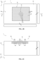
- the view of Figure 2A is along section line II-II of Figure 2B .
- a photoresist mask 32 is provided above a top surface 30a of the semiconductor body 30 by a photolithography step.
- the mask 32 is formed at regions of the semiconductor body 30 wherein it is desired to form the buried cavity 20 and, consequently, the membrane 10 suspended thereon.
- the mask 32 defines a honeycomb lattice, having first mask regions 32a and second mask regions 32b, for example of hexagonal shape in XY plane top view, close to each other and separated from each other by through openings 32c extending through the entire thickness of the mask 32.
- first and the second mask regions 32a, 32b are regions wherein the photoresist material is physically present ("full” regions); the through openings 32c are regions wherein the photoresist material has been removed (“empty” regions) by the photolithographic process, having the top surface 30a of the semiconductor body 30 exposed therethrough.
- the first mask regions 32a have, in top view, a first value of base area; the second mask regions 32b have, in top view, a second value of base area, lower than the first value of base area.
- the mask 32 has portions 34, 36 with full/empty ratio different from each other.
- the portion 34 comprises exclusively the first mask regions 32a and, in the portion 34, the full/empty ratio has a first value (e.g., of the order of 4). Therefore, inside the portion 34, all the first mask regions 32a have the same value of base area (unless there are variations depending on the tolerances of the same process).
- the portion 36 comprises exclusively the second mask regions 32b and, in the portion 36, the full/empty ratio has a second value (e.g., of the order of 2) which is lower than the first value.
- the second value e.g., of the order of 2
- all the second mask regions 32b have the same value of base area (unless there are variations depending on the tolerances of the same process).
- the first mask regions 32a have, as said, hexagonal shape in plan view and diameter (both along the X and Y axis) in the range 2.2-2.6 ⁇ m, and are separated from each other by a gap 32c having extension (both along the X and Y axis) in the range 0.4-0.8 ⁇ m.
- the second mask regions 32b have a hexagonal shape and diameter (both along the X and Y axis) in the range 1.8-2.1 ⁇ m, and are separated from each other by a gap 32c having extension (both along the X and Y axis) in the range 0.9-1.2 ⁇ m.
- an etching of the semiconductor body 30 is performed, forming trenches 38 having depths, along the Z axis, of a few micrometers, for example depth comprised between 0.5 ⁇ m and 50 ⁇ m.
- the trenches 38 define columns 42a, 42b of silicon, having a shape corresponding to the shape of the honeycomb regions defined by the mask 32.
- portions 44, 46 corresponding to the portions 34, 36 of the mask 32 are defined also in the semiconductor body 30; the portion 44 comprises the silicon columns 42a which have shape, dimensions and mutual distance uniform to each other; similarly the portion 46 comprises the silicon columns 42b which have shape, dimensions and mutual distance uniform to each other and different with respect to the portion 44.
- Each column 42a has, in the portion 44, shape and dimensions defined by the portion 34 of the mask 32, for example a hexagonal shape in XY plane plan view, and a diameter equal to about 2.4 ⁇ m, and is separated from an adjacent column, along X and along Y, by about 0.6 ⁇ m.
- Each column 42b has, in the portion 46, shape and dimensions defined by the portion 36 of the mask 32, for example a hexagonal shape in XY plane plan view, and a diameter equal to about 2 ⁇ m, and is separated from an adjacent column, along X and along Y, by about 1 ⁇ m.
- each column 42a has a base area (on the XY plane) which is different from the base area (on the XY plane) of each column 42b.
- the base area (on the XY plane) of the columns 42a is greater than the base area (on the XY plane) of the columns 42b.
- the mutual spacing of the columns 42a, 42b is designed of such a value as to allow a top closure of the trenches 38 during the epitaxial growth step described with reference to Figure 2D .
- the mask 32 is removed.
- an epitaxial growth is performed in a deoxidizing environment (typically, in an atmosphere having a high concentration of hydrogen, preferably using trichlorosilane-SiHCls).
- the epitaxial growth is performed at least until the trenches 38 are closed upwardly (for example, for 45 seconds at a temperature close to 1200°C).
- an epitaxial layer 48 grows above the silicon columns 42a, 42b, closes the trenches 38 upwardly and traps therein the gas present (here, molecules of hydrogen H 2 ) .
- An annealing step is then performed, for example for about 30-40 minutes at a temperature of about 1190-1200°C.
- the annealing step causes, Figure 2E , a migration of the silicon atoms which tend to move to the lower energy position, in a per se known manner, as for example discussed in the article by T. Sato, N. Aoki, I. Mizushima and Y. Tsunashima, "A New Substrate Engineering for the Formation of Empty Space in Silicon (ESS) Induced by Silicon Surface Migration", IEDM 1999, pp. 517-520 .
- the silicon atoms migrate and form the cavity 20 closed upwardly by the epitaxial layer 48 (which, now, forms the membrane 10).
- the annealing is performed in an H 2 atmosphere so as to prevent the hydrogen present in the trenches 38 from escaping through the epitaxial layer towards the outside and to increase the concentration of hydrogen present in the cavity 20 if that trapped during the epitaxial growth step were not sufficient.
- the annealing may be carried out in a nitrogen environment.
- the different shape and mutual distance between the silicon columns, in the portions 44 and 46 of the semiconductor body 30, entails that the migration of the atoms during the annealing step of Figure 2E causes the formation of the cavity 20 as described with reference to Figure 1 , i.e. it leads to the formation of the bumps 11 and 12.
- forming the buried cavity 20 comprises concurrently forming different types of cavities, or sub-cavities, joined to each other and in mutual connection.
- a first type of sub-cavity 24 is formed at the portion 44 and has a maximum extension, along the Z axis, lower than the maximum extension, again along the Z axis, of a second type of sub-cavity 26 which is formed at the portion 46.
- the sub-cavities 24 and 26 are in connection to each other and their typological division is qualitative and not clear-cut.
- the bumps 11, 12 are formed which tend to partially occlude, or locally narrow, the buried cavity 20.
- the Applicant has verified the formation of the first bump 11 at the side 20a that delimits the cavity 20 upwardly, and of the second bump 12 at the side 20b that delimits the cavity 20 downwardly as a direct consequence of the different mutual arrangement and dimension of the silicon columns 42a, 42b and corresponding trenches 38 separating them.
- the silicon columns have a greater base area and are closer to each other (i.e., at the silicon columns 42a) there is formed the sub-cavity 24, with dimension d 1 along the Z axis reduced due to the presence of the bumps 11, 12; where the silicon columns have a smaller base area and are more spaced from each other (i.e., at the silicon columns 42b), there is formed the sub-cavity 26, with dimension d 2 along the Z axis greater than the corresponding dimension d 1 of the sub-cavity 24, as it has no bumps 11, 12.
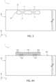
- Figure 3 illustrates, according to a further embodiment, the semiconductor body 30 including the membrane 10 and the cavity 20, wherein the cavity 20 accommodated therein a plurality of bumps 11 (at the top side 20a) and a plurality of bumps 12 (at the bottom side 20b).
- the bumps 11 and 12 are formed as described with reference to Figures 2A-2E .
- Figures 4A-4E illustrate a method for manufacturing the wafer 1 of Figure 1 , in particular for forming the bumps 11, 12, according to an alternative embodiment with respect to that of Figures 2A-2E .
- this may be diced to isolate a plurality of dies or chips manufactured simultaneously as described herein.
- the wafer 1 comprises the semiconductor body 30 (possibly previously processed, as needed, for example including a monocrystalline silicon epitaxial layer grown on a monocrystalline silicon substrate).
- the view of Figure 4A is along section line IV-IV of Figure 4B .
- a photoresist mask 52 is provided above the top surface 30a of the semiconductor body 30 by a photolithography step.
- the mask 52 is formed at regions of the semiconductor body 30 wherein it is desired to form the buried cavity 20 and, consequently, the membrane 10 suspended thereon.
- the mask 52 defines a honeycomb lattice, having mask regions 52a for example of hexagonal shape, close to each other and separated from each other by through openings 52c extending through the entire thickness of the mask 52.
- a second mask region 52b has no through openings 52c.
- first and the second mask regions 52a, 52b are regions wherein the photoresist material is physically present ("full” regions); the through openings 52c are regions wherein the photoresist material has been removed (“empty” regions) by the photolithographic process, having the top surface 30a of the semiconductor body 30 exposed therethrough.
- the first mask regions 52a have, in top view, a first value of base area; the second mask region 52b has, in top view, a second value of base area, greater than the first value of base area.
- the portion of the mask 52 wherein the first mask regions 52a are present has a full/empty ratio of the type already described for the portion 36 of the mask 52 of Figure 2A or 2B .
- the portion of the mask 52 wherein the second mask region 52b is present has no empty spaces.
- the first mask regions 52a have a hexagonal shape and diameter (both along the X and Y axis) in the range 1.8-2.1 ⁇ m, and are separated from each other by a gap 32c having extension (both along the X and Y axis) in the range 0.9-1.2 ⁇ m.
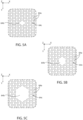
- the second mask region 52b has any shape (e.g. generically polygonal), chosen during the design step, for example of the type illustrated in Figures 5A-5C according to the respective embodiments.
- an etching of the semiconductor body 30 is performed, forming trenches 58 having depths, along the Z axis, of a few micrometers, for example depth comprised between 0.5 ⁇ m and 50 pm.
- the trenches 58 define columns 62a, 62b of silicon having a shape corresponding to the shape of the regions 52a, 52b defined by the mask 52.
- silicon columns 62a are formed which have shape, dimensions and mutual distance uniform to each other, as determined by the first mask region 52a; similarly, a single silicon column 62b is formed, contiguous to the silicon columns 62a (in particular, surrounded by the silicon columns 62a, at a distance determined by the trenches 58), which has a shape and dimensions defined by the second mask region 52b.
- Each column 62a has, for example, a hexagonal shape with a diameter equal to about 2 ⁇ m, and is separated from an adjacent column 62a, along X and along Y, by about 1 ⁇ m.
- diameter and spacing of the columns 62a are designed of such a value as to allow a top closure of the trenches 58 during the epitaxial growth step described with reference to Figure 4D .
- the mask 52 is removed.
- an epitaxial growth is performed in a deoxidizing environment (typically, in an atmosphere having a high concentration of hydrogen, preferably using trichlorosilane-SiHCl 3 ).
- the epitaxial growth is performed at least until the trenches 58 are closed upwardly (for example, for 45 seconds at a temperature close to 1200°C).
- an epitaxial layer 70 grows above the silicon columns 62a, 62b, closes the trenches 58 upwardly and traps therein the gas present (here, molecules of hydrogen H 2 ) .
- An annealing step is then performed, for example for about 30-40 minutes at a temperature of about 1190-1200°C.
- the annealing step causes, Figure 4E , a migration of the silicon atoms which tend to move to the lower energy position, in a per se known manner, as for example discussed in the article by T. Sato, N. Aoki, I. Mizushima and Y. Tsunashima, "A New Substrate Engineering for the Formation of Empty Space in Silicon (ESS) Induced by Silicon Surface Migration", IEDM 1999, pp. 517-520 .
- the silicon atoms migrate and form the cavity 20 closed upwardly by the epitaxial layer 70 (which, now, forms the membrane 10).
- the annealing is performed in an H 2 atmosphere so as to prevent the hydrogen present in the trenches 58 from escaping through the epitaxial layer towards the outside and to increase the concentration of hydrogen present in the cavity 20 if that trapped during the epitaxial growth step were not sufficient.
- the annealing may be carried out in a nitrogen environment.
- forming the buried cavity 20 comprises concurrently forming different types of cavities, or sub-cavities, joined to each other and in mutual connection.
- a first type of sub-cavity 74 is formed at the silicon column 62b, and a second type of sub-cavity 75 is formed at the silicon columns 62a.
- the sub-cavity 74 of the first type has a maximum extension, along the Z axis, lower than the maximum extension, along the Z axis, of the second type of sub-cavity 75.
- the typological division among the sub-cavities of different type is qualitative and not clear-cut.
- the bumps 11, 12 are formed at the sub-cavity 74 of the first type and tend to partially occlude, or locally narrow, the buried cavity 20.
- Figure 4E illustrates, for simplicity of representation, bumps 11, 12 having the same thickness along the Z axis
- the advantageous effect of the present invention would be obtained even if (by variation in the process parameters) one of the bumps 11, 12 protruded from the respective side for a maximum thickness, along Z, greater than the corresponding maximum thickness of the other bump 11, 12.
- one of the bumps 11 and 12 might be absent.
- Figure 5A illustrates, in XY plane view, a layout of the column, or pillar, 62b.
- the column 62b has the shape of a four-pointed "star” or of a "cross”, of maximum dimension (from tip to tip), along X and along Y equal to a few micrometers, for example 7 ⁇ m along the X axis and 5 ⁇ m along the Y axis.
- Figure 5B illustrates, in XY plane view, a further layout of the column, or pillar, 62b.
- the column 62b has the shape of a six-pointed "star", and for example maximum dimension (from tip to tip), along Y equal for example to 8 ⁇ m and minimum dimension, along X, equal for example to 6 ⁇ m.
- Figure 5C illustrates, in XY plane view, a further layout of the column, or pillar, 62b.
- the column 62b has the shape of a twelve-pointed "star” or “flower”, and the maximum dimension (from tip to tip), along X or along Y, comprised for example between 12 and 14 ⁇ m.
- Figures 6A-6G illustrate a manufacturing method of the wafer 1, in particular of the membrane 10 suspended on the buried cavity 20 which includes at least the bump 11, according to a further embodiment of the present invention.
- the wafer 1 may be diced to isolate a plurality of dies or chips manufactured simultaneously as described herein.
- the wafer 1 comprises the semiconductor body 30, here of monocrystalline silicon.
- a photoresist mask 83 is provided above the top surface 30a of the semiconductor body 30 by a photolithography step. The mask 83 is formed at regions of the semiconductor body 30 wherein it is desired to form the cavity 20.
- the mask 83 defines a honeycomb lattice, having mask regions, for example of a hexagonal shape, close to each other.
- each column 87 has a diameter equal to about 1 ⁇ m and is separated from an adjacent column, along X or along Y, by about 1 ⁇ m. In general, diameter and spacing of the columns 87 are chosen of such a value as to allow a top closure of the trenches 86 during the epitaxial growth step described hereinbelow.
- the mask 83 is removed and an epitaxial growth is performed in a deoxidizing environment (typically, in an atmosphere having a high concentration of hydrogen, preferably using trichlorosilane-SiHCls).
- the epitaxial growth is performed at least until the trenches 86 are closed upwardly (for example, for 45 seconds at a temperature close to 1200°C).
- a sealing layer 88 (hereinafter forming, at least in part, the membrane 10), is grown epitaxially above the silicon columns 87; the sealing layer 88 closes the trenches 86 upwardly and traps therein the gas present (here, molecules of hydrogen H 2 ) .
- An annealing step is then performed, for example for about 30-40 minutes at a temperature of about 1190-1200°C.
- the annealing step causes, Figure 6E , a migration of the silicon atoms which tend to move to the lower energy position, in a per se known manner, as for example discussed in the article by T. Sato, N. Aoki, I. Mizushima and Y. Tsunashima, "A New Substrate Engineering for the Formation of Empty Space in Silicon (ESS) Induced by Silicon Surface Migration", IEDM 1999, pp. 517-520 .
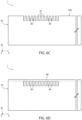
- the silicon atoms migrate completely and form the cavity 20, closed upwardly by the sealing layer 88, of Silicon.
- the annealing is performed in an H 2 atmosphere so as to prevent the hydrogen present in the trenches 86 from escaping through the epitaxial layer towards the outside and to increase the concentration of hydrogen present in the cavity 20 if that trapped during the epitaxial growth step were not sufficient.
- the annealing may be carried out in a nitrogen environment.
- the sealing layer 88 is selectively removed at a portion thereof wherein the bump 11 is intended to be formed.
- a chemical etching (arrows 90 in Figure 6F ) is performed using an etching mask 92 to form an opening 89 passing through the entire thickness of the sealing layer 88.
- the through opening 89 reaches the cavity 20, putting it in connection with the external environment.
- the through opening 89 has, for example, a circular or generically polygonal shape in XY plane view, for example with a diameter comprised between 0.1 and 5 ⁇ m, more particularly between 0.1 and 1 ⁇ m, even more particularly between 0.1 and 0.3 ⁇ m.
- the through opening 89 may also have irregular shapes, or for example one of the shapes and dimensions illustrated in Figures 5A-5C for the element 62b.
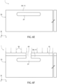
- an epitaxial growth step is performed at the sealing layer 88, such that it closes the through opening 89 thus isolating the cavity 20 from the external environment.
- the Silicon also grows epitaxially towards the inside of the cavity 20, at the through opening 89, forming a protuberance that extends towards the inside of the cavity 20.
- the through opening 89 closes and this protuberance forms the bump 11.
- the cavity 20, at the end of the method is buried in the semiconductor body 30 and its internal pressure is defined by the pressure present in the reaction chamber during the epitaxial growth leading to the formation of the bump 11.
- the membrane 10 may be thinned, if necessary, for example by CMP technique.
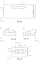
- Figures 7A-7C illustrate a further technical solution for manufacturing a buried cavity provided with one or more bumps.
- Figures 7A-7C are illustrated in a triaxial reference system of X, Y, Z axes orthogonal to each other. Reference will be made hereinafter to the processing of wafers; however, what has been described applies similarly to the processing of portions of a semiconductor wafer, for example dies. Similarly, at the end of the processing steps of the wafers, these may be diced ("dicing" operation) to isolate a plurality of dies or chips manufactured simultaneously as described herein.
- a first wafer 100 of semiconductor material for example of Silicon, is shaped so as to form, at one front side 100a thereof, a recess 102 having a bottom side 102a.
- the bottom side 102a has a protuberance, or bump, 104, for example having a circular, polygonal or irregular shape, which extends moving away from the bottom side 102a.
- the bump 104 may have one of the shapes described and illustrated with reference to Figures 5A-5C for the element 62b.
- the bump 104 extends, from the bottom side 102a, for a height, along the Z axis, comprised between 0.01 and 1 ⁇ m (in particular between 0.1 and 1 ⁇ m).
- a second wafer 110 of semiconductor material is arranged, having a front side 112a and a rear side 110b opposite to each other along the Z axis.
- the second wafer 110 is for example of Silicon.
- the second wafer 110 is shaped so as to form, at the front side 112a, a recess 112 having a bottom side 112a.
- the bottom side 112a has a protuberance, or bump, 114, for example having a circular, polygonal or irregular shape.
- the bump 114 may have one of the shapes described and illustrated with reference to Figures 5A-5C for the element 62b.
- the bump 114 extends, from the bottom side 112a, for a height, along the Z axis, comprised between 0.01 and 1 ⁇ m (in particular between 0.1 and 1 pm).
- the bumps 104 and 114 are formed in such a way that, when the first and the second wafers 100, 110 are coupled to each other as described with reference to Figure 7C , the bumps 104 and 114 are at least partially aligned with each other along the direction of the Z axis.
- the first wafer 100 and the second wafer 110 are coupled to each other at coupling regions 108 extending laterally to (i.e., surrounding) the recesses 102, 112.
- the coupling may be carried out by per se known wafer- to-wafer bonding techniques. For example, it is possible to use glue, double-sided adhesive layers, glass frit, etc.
- the coupling between the wafers 100, 110 is performed in such a way that the recesses 102, 112 form, together, a cavity 120 fluidically isolated from the external environment.
- the second wafer 110 thus forms, at its rear side 110b, a membrane 121 suspended on the cavity 120. It is possible to thin the second wafer 110 at the rear side 110b to obtain a desired thickness for the membrane 121.
- the membrane 121 is for bending when a suitable external force F is applied along the Z direction as identified by arrow 124. At rest, when no external force F acts on the membrane 121, the membrane 121 is substantially parallel to the XY plane. In the presence of a suitable force F, the membrane 121 bends, and, as the force F increases, the membrane 121 bends up to a maximum bending point wherein the bumps 104, 114 are in mutual contact.
- the bumps 104, 114 operate, in this context, as antistiction structures, minimizing the risk of irreversible stiction between the opposite sides 102a, 112a internal to the cavity 120 when, during use, the opposite sides 102a, 112a come close to each other.
- the contact occurs exclusively between the bumps 104, 114 which have a reduced contact surface and, therefore, also the stiction forces are consequently reduced.
- the second wafer 110 is shaped so as not to have the bump 114.
- the cavity 120 accommodates the sole bump 104.
- one of or both the first and the second wafers 100, 110 may be shaped so as to have a plurality of bumps 104 and/or a plurality of bumps 114, with shapes and dimensions equal to or different from each other.
- the present invention may find application as a pressure sensor (in particular of differential type), or as a fluidic micro-valve or fluidic micro-pump with an actuation that is, in particular, piezoelectric.
- the transduction of the signal applied on the membrane 10, 110 may occur according to any of the known techniques, for example by forming piezoresistors on the membrane 10, 110, or in proximity thereto, in a manner known per se and not an object of the present invention.
- the piezoresistive elements have P-type conductivity and the membrane has N-type conductivity (the electrical conductivities are obtained by implanting dopant species, in a per se known manner).
- the piezoresistors may be made of polysilicon above the membrane.
- FIG. 7A-7C , or 8A-8B is suitable for manufacturing a capacitive pressure sensor, using coupling regions 108 which electrically insulate the two wafers 100, 110 which form the two electrons, or plates, of a capacitor.
- a pressure on the membrane 121 it deflects, reducing its distance from the bottom electrode (wafer 100).
- the capacitance of the sensing capacitor increases.
- an indication of the applied pressure force F
- the present invention allows antistiction structures to be provided inside a buried cavity, maintaining a desired pressure (defined during the design step) of the cavity.
- the cavity has an internal pressure lower than the atmospheric pressure wherein the structure thus formed is designed to operate.
- the layout of the buried cavity 20, 120 may be freely designed according to parameters that are not an object of the present invention.
- the buried cavity 20, 120 may have, in XY plane plan view, a shape chosen from quadrangular, circular, quadrangular with rounded edges, polygonal, irregular.
- hexagonal or honeycomb shape of the base area 8 (in XY plane view) of the columnar structures 42a, 42b may be different, i.e. generically polygonal or circular.
- the shape of the columnar structures 42a, 42b may further vary; for example they may be replaced by septa of semiconductor material, or in general by other thin structures capable of allowing the migration of silicon during the annealing step, favoring or allowing the formation of the buried cavity.
Landscapes
- Engineering & Computer Science (AREA)
- Microelectronics & Electronic Packaging (AREA)
- Manufacturing & Machinery (AREA)
- Computer Hardware Design (AREA)
- Chemical & Material Sciences (AREA)
- Analytical Chemistry (AREA)
- Pressure Sensors (AREA)
Abstract

Description
- The present disclosure relates to a micromechanical or microelectromechanical structure, to manufacturing methods thereof, and to a MEMS transducer; in particular, this structure includes a buried cavity having one or more antistiction bumps extending therein.
- As known, integrated pressure sensors may be provided with micromanufacturing techniques. These sensors typically comprise a thin membrane, or diaphragm, suspended above a cavity obtained in a semiconductor body. Piezoresistive elements connected to each other are formed within the membrane and connected in a Wheatstone bridge. When subject to a pressure, the membrane undergoes a deformation, causing a variation in the resistance of the piezoresistive elements, and therefore an imbalance of the Wheatstone bridge. Alternatively, capacitive sensors are available, wherein the membrane provides a first plate of a capacitor, while a second plate is provided by a fixed reference. In use, the deflection of the membrane generates a variation in the capacitance of the capacitor, which may be detected and associated with the pressure exerted on the membrane.
- A significant defect, which occurs in particular conditions in micromechanical devices, is the irreversible stiction of the movable structures with a fixed element adjacent thereto, or to the substrate. It is apparent that this phenomenon may entail serious consequences, up to making the MEMS systems affected thereby inoperative, in an unpredictable way. In particular, in case of a membrane, the stiction of the membrane to the substrate on which the membrane is suspended makes it unusable.
- The stiction phenomenon is typically generated by the surface forces that are exerted between the surfaces of two bodies coming into contact. Of course, the wider the contact zone, the greater the interaction force between the surfaces. In addition, further factors that are to be considered in assessing and preventing stiction are, inter alia, the roughness of the surfaces, their wear, the level of humidity and the temperature of the environment wherein the micromechanical structures operate. These parameters are particularly difficult to monitor in case of membranes suspended on buried cavities, due to the inherent difficulty of operating internally to these buried cavities to reduce the causes of stiction.
- A possible solution lies in the stiffening of the membrane, so that it never reaches the full stroke during use and no direct contact occurs between the opposite surfaces delimiting the cavity having the membrane suspended thereon. For example, it is possible to increase the stiffness of the membrane by increasing the thickness of the membrane. In manufacturing processes of known semiconductor pressure sensors, the membrane is formed by an epitaxial growth. The increase in the epitaxial growth time, necessary to obtain a thicker membrane, has several drawbacks such as, for example, an increase in costs and an increase in the non-uniformity of the rear side of the semiconductor wafer, which cause difficulties in handling the wafer and incompatibility problems with subsequent steps of the manufacturing process. Furthermore, the known integrated semiconductor pressure sensors are typically designed and used to measure relatively low pressures (for example up to 0.1 MPa), and a stiffening of the membrane thereof might cause an operating difficulty at such pressures.
-
EP2075224 relates to the field of micromechanical and/or nanomechanical devices comprising mobile elements, and more particularly that of microelectromechanical systems (MEMS) and/or nanoelectromechanical systems (NEMS) comprising mobile elements capable of coming into contact with other elements of the MEMS and/or NEMS during its operation. -
US 2021/285983 relates to a physical quantity sensor, an electronic apparatus, and a vehicle. -
US 2005/181529 relates to a method for manufacturing a semiconductor component. -
EP3845485 relates to the field of temperature sensor, and in particular to a manufacturing method for a temperature sensor, and a temperature sensor. - However, the above-mentioned issues are not solved.
- The aim of the present invention is to provide a structure, manufacturing methods thereof, and a microelectromechanical transducer, for overcoming the drawbacks of the prior art.
- According to the present invention, a structure, manufacturing methods thereof, and a microelectromechanical transducer are provided, as defined in the appended claims.
- For a better understanding of the present invention, preferred embodiments thereof are now described, purely by way of non-limiting example, with reference to the attached drawings, wherein:
-
Figure 1 illustrates, in lateral sectional view, a micromechanical structure according to an embodiment of the present invention; -
Figures 2A-2E illustrate steps of a manufacturing process of the micromechanical structure ofFigure 1 ; -
Figure 3 illustrates, in lateral sectional view, a micromechanical structure according to a further embodiment of the present invention; -
Figures 4A-4E illustrate steps of a manufacturing process of the micromechanical structure ofFigure 3 ; -
Figures 5A-5C illustrate, in plan view, a layout of the micromechanical structure ofFigure 3 in an intermediate manufacturing step; -
Figures 6A-6G illustrate steps of a manufacturing process of the micromechanical structure ofFigure 1 orFigure 3 according to a further embodiment of the present invention; -
Figures 7A-7C illustrate a manufacturing method of the micromechanical structure ofFigure 1 orFigure 3 according to a further embodiment of the present invention; and -
Figures 8A and 8B illustrate a variant of the manufacturing method ofFigures 7A-7C . -
Figure 1 illustrates, in a triaxial system of X, Y, Z axes orthogonal to each other, a portion of asemiconductor wafer 1 including a micromechanical or microelectromechanical (MEMS) structure according to an embodiment of the present invention. However, it is apparent that what has been described applies similarly to a portion of a semiconductor wafer, for example to a die. Similarly, at the end of the processing steps of the wafer, this may be diced ("dicing" operation) to isolate a plurality of dies or chips. - The
wafer 1, or die, comprises asemiconductor body 30 which accommodates amembrane 10 suspended on acavity 20 buried in thesemiconductor body 30. Thecavity 20 is delimited upwardly by a top side (or wall) 20a (which is part of the membrane 10) and downwardly by a bottom side (or wall) 20b (which is part of the semiconductor body 30), opposite to thetop side 20a along the Z axis. Lateral sides (or walls) 20c physically connect thetop side 20a with thebottom side 20b. - In one embodiment, the
membrane 10 extends, at rest, substantially parallel to the XY plane. It is however possible to design themembrane 10 having internal stresses such that themembrane 10 extends, at rest, not perfectly parallel to the XY plane, but with a concave or convex shape. In the following of the present description and in the Figures it is assumed, for simplicity of description and representation, that themembrane 10 is parallel to the XY plane. - The
cavity 20 has one or more protrusions, or protuberances, or "bumps", 11 which extend from thetop side 20a towards thebottom side 20b, and vice versa, one or more protrusions, or protuberances, or "bumps", 12 which extend from thebottom side 20b towards thetop side 20a. For sake of simplicity,Figure 1 illustrates asingle bump 11 and asingle bump 12. - In a further embodiment, not illustrated, one of the
bump 11 and thebump 12 may be omitted. - The
membrane 10 is therefore partially suspended on thecavity 20 and is for bending when a suitable external force F is applied along the direction Z as identified by thearrow 14. At rest, when no external force F acts on themembrane 10, themembrane 10 is substantially parallel to the XY plane. In the presence of a suitable force F, themembrane 10 bends, and, as the force F increases, themembrane 10 bends up to a maximum bending wherein thebumps - The
bumps opposite sides cavity 20 when, during use, thesides bumps - With reference to
Figures 2A-2E , a manufacturing method of themembrane 10 on the buriedcavity 20 in thesemiconductor body 30 is described. - The
wafer 1 is, in particular, of monocrystalline silicon; thewafer 1 may be N-type or P-type doped (the type of doping is not relevant for the present invention, and may be defined during the design step according to the specific application wherein the present technical solution is intended to operate). - As previously noted, reference will be made hereinafter to the processing of a wafer; however, what has been described applies similarly to the processing of portions of a semiconductor wafer, for example a die. Similarly, at the end of the processing steps of the
wafer 1, this may be diced ("dicing" operation) to isolate a plurality of dies or chips manufactured simultaneously as described herein. - With joint reference to
Figure 2A (in lateral sectional view) and toFigure 2B (in XY plane top view), thewafer 1 comprises the semiconductor body 30 (possibly previously processed, as needed, for example including a monocrystalline silicon epitaxial layer grown on a monocrystalline silicon substrate). The view ofFigure 2A is along section line II-II ofFigure 2B . - A
photoresist mask 32 is provided above atop surface 30a of thesemiconductor body 30 by a photolithography step. Themask 32 is formed at regions of thesemiconductor body 30 wherein it is desired to form the buriedcavity 20 and, consequently, themembrane 10 suspended thereon. - The
mask 32 defines a honeycomb lattice, havingfirst mask regions 32a andsecond mask regions 32b, for example of hexagonal shape in XY plane top view, close to each other and separated from each other by throughopenings 32c extending through the entire thickness of themask 32. - In particular, the first and the
second mask regions openings 32c are regions wherein the photoresist material has been removed ("empty" regions) by the photolithographic process, having thetop surface 30a of thesemiconductor body 30 exposed therethrough. - The
first mask regions 32a have, in top view, a first value of base area; thesecond mask regions 32b have, in top view, a second value of base area, lower than the first value of base area. - In other words, according to an aspect of the present invention, the
mask 32 hasportions portion 34 comprises exclusively thefirst mask regions 32a and, in theportion 34, the full/empty ratio has a first value (e.g., of the order of 4). Therefore, inside theportion 34, all thefirst mask regions 32a have the same value of base area (unless there are variations depending on the tolerances of the same process). - Similarly, the
portion 36 comprises exclusively thesecond mask regions 32b and, in theportion 36, the full/empty ratio has a second value (e.g., of the order of 2) which is lower than the first value. Within theportion 36, all thesecond mask regions 32b have the same value of base area (unless there are variations depending on the tolerances of the same process). - By way of example, in the
portion 34, thefirst mask regions 32a have, as said, hexagonal shape in plan view and diameter (both along the X and Y axis) in the range 2.2-2.6 µm, and are separated from each other by agap 32c having extension (both along the X and Y axis) in the range 0.4-0.8 µm. In theportion 36, thesecond mask regions 32b have a hexagonal shape and diameter (both along the X and Y axis) in the range 1.8-2.1 µm, and are separated from each other by agap 32c having extension (both along the X and Y axis) in the range 0.9-1.2 µm. - By using the
mask 32,Figure 2C , an etching of thesemiconductor body 30 is performed, formingtrenches 38 having depths, along the Z axis, of a few micrometers, for example depth comprised between 0.5 µm and 50 µm. Thetrenches 38 definecolumns mask 32. - Therefore,
portions portions mask 32 are defined also in thesemiconductor body 30; theportion 44 comprises thesilicon columns 42a which have shape, dimensions and mutual distance uniform to each other; similarly theportion 46 comprises thesilicon columns 42b which have shape, dimensions and mutual distance uniform to each other and different with respect to theportion 44. - Each
column 42a has, in theportion 44, shape and dimensions defined by theportion 34 of themask 32, for example a hexagonal shape in XY plane plan view, and a diameter equal to about 2.4 µm, and is separated from an adjacent column, along X and along Y, by about 0.6 µm. - Each
column 42b has, in theportion 46, shape and dimensions defined by theportion 36 of themask 32, for example a hexagonal shape in XY plane plan view, and a diameter equal to about 2 µm, and is separated from an adjacent column, along X and along Y, by about 1 µm. - In other words, each
column 42a has a base area (on the XY plane) which is different from the base area (on the XY plane) of eachcolumn 42b. The base area (on the XY plane) of thecolumns 42a is greater than the base area (on the XY plane) of thecolumns 42b. - In general, the mutual spacing of the
columns trenches 38 during the epitaxial growth step described with reference toFigure 2D . - After the formation of the
columns mask 32 is removed. - With reference to
Figure 2D , an epitaxial growth is performed in a deoxidizing environment (typically, in an atmosphere having a high concentration of hydrogen, preferably using trichlorosilane-SiHCls). The epitaxial growth is performed at least until thetrenches 38 are closed upwardly (for example, for 45 seconds at a temperature close to 1200°C). - Consequently, an
epitaxial layer 48 grows above thesilicon columns trenches 38 upwardly and traps therein the gas present (here, molecules of hydrogen H2) . - An annealing step is then performed, for example for about 30-40 minutes at a temperature of about 1190-1200°C. The annealing step causes,
Figure 2E , a migration of the silicon atoms which tend to move to the lower energy position, in a per se known manner, as for example discussed in the article by T. Sato, N. Aoki, I. Mizushima and Y. Tsunashima, "A New Substrate Engineering for the Formation of Empty Space in Silicon (ESS) Induced by Silicon Surface Migration", IEDM 1999, pp. 517-520. - At the
trenches 38, where the silicon columns are close to each other, the silicon atoms migrate and form thecavity 20 closed upwardly by the epitaxial layer 48 (which, now, forms the membrane 10). - Preferably, the annealing is performed in an H2 atmosphere so as to prevent the hydrogen present in the
trenches 38 from escaping through the epitaxial layer towards the outside and to increase the concentration of hydrogen present in thecavity 20 if that trapped during the epitaxial growth step were not sufficient. Alternatively, the annealing may be carried out in a nitrogen environment. - The different shape and mutual distance between the silicon columns, in the
portions semiconductor body 30, entails that the migration of the atoms during the annealing step ofFigure 2E causes the formation of thecavity 20 as described with reference toFigure 1 , i.e. it leads to the formation of thebumps - In practice, forming the buried
cavity 20 comprises concurrently forming different types of cavities, or sub-cavities, joined to each other and in mutual connection. A first type ofsub-cavity 24 is formed at theportion 44 and has a maximum extension, along the Z axis, lower than the maximum extension, again along the Z axis, of a second type ofsub-cavity 26 which is formed at theportion 46. The sub-cavities 24 and 26 are in connection to each other and their typological division is qualitative and not clear-cut. According to the present invention, at the sub-cavity 24, thebumps cavity 20. - The Applicant has verified the formation of the
first bump 11 at theside 20a that delimits thecavity 20 upwardly, and of thesecond bump 12 at theside 20b that delimits thecavity 20 downwardly as a direct consequence of the different mutual arrangement and dimension of thesilicon columns corresponding trenches 38 separating them. Where the silicon columns have a greater base area and are closer to each other (i.e., at thesilicon columns 42a) there is formed the sub-cavity 24, with dimension d1 along the Z axis reduced due to the presence of thebumps silicon columns 42b), there is formed the sub-cavity 26, with dimension d2 along the Z axis greater than the corresponding dimension d1 of the sub-cavity 24, as it has nobumps - For example, it is d1=1.5-2 µm and d2=2.1-2.5 µm.
- Although the Figures illustrate, for sake of simplicity, bumps 11, 12 having the same thickness along the Z axis, the advantageous effect of the present invention would be obtained even if (by variation in the process parameters) a bump protruded from the respective side for a maximum thickness, along Z, greater than the corresponding maximum thickness of the other bump. Similarly, one of the
bumps -
Figure 3 illustrates, according to a further embodiment, thesemiconductor body 30 including themembrane 10 and thecavity 20, wherein thecavity 20 accommodated therein a plurality of bumps 11 (at thetop side 20a) and a plurality of bumps 12 (at thebottom side 20b). In this embodiment, thebumps Figures 2A-2E . -
Figures 4A-4E illustrate a method for manufacturing thewafer 1 ofFigure 1 , in particular for forming thebumps Figures 2A-2E . As previously noted, what has been described applies similarly to the processing of a die. At the end of the processing steps of thewafer 1, this may be diced to isolate a plurality of dies or chips manufactured simultaneously as described herein. - With joint reference to
Figure 4A (in lateral sectional view) and toFigure 4B (in XY plane top view), thewafer 1 comprises the semiconductor body 30 (possibly previously processed, as needed, for example including a monocrystalline silicon epitaxial layer grown on a monocrystalline silicon substrate). The view ofFigure 4A is along section line IV-IV ofFigure 4B . - A
photoresist mask 52 is provided above thetop surface 30a of thesemiconductor body 30 by a photolithography step. Themask 52 is formed at regions of thesemiconductor body 30 wherein it is desired to form the buriedcavity 20 and, consequently, themembrane 10 suspended thereon. - The
mask 52 defines a honeycomb lattice, havingmask regions 52a for example of hexagonal shape, close to each other and separated from each other by throughopenings 52c extending through the entire thickness of themask 52. Asecond mask region 52b has no throughopenings 52c. - In particular, the first and the
second mask regions openings 52c are regions wherein the photoresist material has been removed ("empty" regions) by the photolithographic process, having thetop surface 30a of thesemiconductor body 30 exposed therethrough. - The
first mask regions 52a have, in top view, a first value of base area; thesecond mask region 52b has, in top view, a second value of base area, greater than the first value of base area. - In other words, according to an aspect of the present invention, the portion of the
mask 52 wherein thefirst mask regions 52a are present has a full/empty ratio of the type already described for theportion 36 of themask 52 ofFigure 2A or2B . The portion of themask 52 wherein thesecond mask region 52b is present has no empty spaces. - By way of example, the
first mask regions 52a have a hexagonal shape and diameter (both along the X and Y axis) in the range 1.8-2.1 µm, and are separated from each other by agap 32c having extension (both along the X and Y axis) in the range 0.9-1.2 µm. - The
second mask region 52b has any shape (e.g. generically polygonal), chosen during the design step, for example of the type illustrated inFigures 5A-5C according to the respective embodiments. - By using the
mask 52,Figure 4C , an etching of thesemiconductor body 30 is performed, formingtrenches 58 having depths, along the Z axis, of a few micrometers, for example depth comprised between 0.5 µm and 50 pm. Thetrenches 58 definecolumns regions mask 52. Therefore, also in thesemiconductor body 30silicon columns 62a are formed which have shape, dimensions and mutual distance uniform to each other, as determined by thefirst mask region 52a; similarly, asingle silicon column 62b is formed, contiguous to thesilicon columns 62a (in particular, surrounded by thesilicon columns 62a, at a distance determined by the trenches 58), which has a shape and dimensions defined by thesecond mask region 52b. - Each
column 62a has, for example, a hexagonal shape with a diameter equal to about 2 µm, and is separated from anadjacent column 62a, along X and along Y, by about 1 µm. In general, diameter and spacing of thecolumns 62a are designed of such a value as to allow a top closure of thetrenches 58 during the epitaxial growth step described with reference toFigure 4D . - After the formation of the
columns mask 52 is removed. - With reference to
Figure 4D , an epitaxial growth is performed in a deoxidizing environment (typically, in an atmosphere having a high concentration of hydrogen, preferably using trichlorosilane-SiHCl3). The epitaxial growth is performed at least until thetrenches 58 are closed upwardly (for example, for 45 seconds at a temperature close to 1200°C). - Consequently, an
epitaxial layer 70 grows above thesilicon columns trenches 58 upwardly and traps therein the gas present (here, molecules of hydrogen H2) . - An annealing step is then performed, for example for about 30-40 minutes at a temperature of about 1190-1200°C. The annealing step causes,
Figure 4E , a migration of the silicon atoms which tend to move to the lower energy position, in a per se known manner, as for example discussed in the article by T. Sato, N. Aoki, I. Mizushima and Y. Tsunashima, "A New Substrate Engineering for the Formation of Empty Space in Silicon (ESS) Induced by Silicon Surface Migration", IEDM 1999, pp. 517-520. - At the
trenches 58, where the silicon columns are close to each other, the silicon atoms migrate and form thecavity 20 closed upwardly by the epitaxial layer 70 (which, now, forms the membrane 10). - Preferably, the annealing is performed in an H2 atmosphere so as to prevent the hydrogen present in the
trenches 58 from escaping through the epitaxial layer towards the outside and to increase the concentration of hydrogen present in thecavity 20 if that trapped during the epitaxial growth step were not sufficient. Alternatively, the annealing may be carried out in a nitrogen environment. - The mutual distance between the
silicon columns 62a, and the distance between thesilicon columns 62a and thesilicon column 62b, entails that the migration of the atoms during the annealing step ofFigure 4E shapes thecavity 20 in analogy to what has been described with reference toFigure 1 , i.e. leads to the formation of thebumps - Similarly to what has been previously observed, forming the buried
cavity 20 comprises concurrently forming different types of cavities, or sub-cavities, joined to each other and in mutual connection. A first type ofsub-cavity 74 is formed at thesilicon column 62b, and a second type ofsub-cavity 75 is formed at thesilicon columns 62a. Thesub-cavity 74 of the first type has a maximum extension, along the Z axis, lower than the maximum extension, along the Z axis, of the second type ofsub-cavity 75. The typological division among the sub-cavities of different type is qualitative and not clear-cut. According to the present invention, thebumps sub-cavity 74 of the first type and tend to partially occlude, or locally narrow, the buriedcavity 20. - Although
Figure 4E illustrates, for simplicity of representation, bumps 11, 12 having the same thickness along the Z axis, the advantageous effect of the present invention would be obtained even if (by variation in the process parameters) one of thebumps other bump bumps -
Figure 5A illustrates, in XY plane view, a layout of the column, or pillar, 62b. In this embodiment, thecolumn 62b has the shape of a four-pointed "star" or of a "cross", of maximum dimension (from tip to tip), along X and along Y equal to a few micrometers, for example 7 µm along the X axis and 5 µm along the Y axis. -
Figure 5B illustrates, in XY plane view, a further layout of the column, or pillar, 62b. In this embodiment, thecolumn 62b has the shape of a six-pointed "star", and for example maximum dimension (from tip to tip), along Y equal for example to 8 µm and minimum dimension, along X, equal for example to 6 µm. -
Figure 5C illustrates, in XY plane view, a further layout of the column, or pillar, 62b. In this embodiment, thecolumn 62b has the shape of a twelve-pointed "star" or "flower", and the maximum dimension (from tip to tip), along X or along Y, comprised for example between 12 and 14 µm. -
Figures 6A-6G illustrate a manufacturing method of thewafer 1, in particular of themembrane 10 suspended on the buriedcavity 20 which includes at least thebump 11, according to a further embodiment of the present invention. As previously noted, what has been described applies similarly to the processing of a die. At the end of the processing steps of thewafer 1, this may be diced to isolate a plurality of dies or chips manufactured simultaneously as described herein. - With joint reference to
Figure 6A (in lateral sectional view) and toFigure 6B (in top view), thewafer 1 comprises thesemiconductor body 30, here of monocrystalline silicon. Aphotoresist mask 83 is provided above thetop surface 30a of thesemiconductor body 30 by a photolithography step. Themask 83 is formed at regions of thesemiconductor body 30 wherein it is desired to form thecavity 20. - The
mask 83 defines a honeycomb lattice, having mask regions, for example of a hexagonal shape, close to each other. - By using the
mask 83,Figure 6C , an etching of thesemiconductor body 30 is performed, formingtrenches 86 having depths of a few micrometers, for example comprised between 5 µm and 25 µm. Thetrenches 86 definesilicon columns 87 substantially equal to each other and of a shape corresponding to the shape of the honeycomb regions defined by themask 83. Exemplarily, eachcolumn 87 has a diameter equal to about 1 µm and is separated from an adjacent column, along X or along Y, by about 1 µm. In general, diameter and spacing of thecolumns 87 are chosen of such a value as to allow a top closure of thetrenches 86 during the epitaxial growth step described hereinbelow. - Subsequently,
Figure 6D , themask 83 is removed and an epitaxial growth is performed in a deoxidizing environment (typically, in an atmosphere having a high concentration of hydrogen, preferably using trichlorosilane-SiHCls). The epitaxial growth is performed at least until thetrenches 86 are closed upwardly (for example, for 45 seconds at a temperature close to 1200°C). - Consequently, a sealing layer 88 (hereinafter forming, at least in part, the membrane 10), is grown epitaxially above the
silicon columns 87; thesealing layer 88 closes thetrenches 86 upwardly and traps therein the gas present (here, molecules of hydrogen H2) . - An annealing step is then performed, for example for about 30-40 minutes at a temperature of about 1190-1200°C. The annealing step causes,
Figure 6E , a migration of the silicon atoms which tend to move to the lower energy position, in a per se known manner, as for example discussed in the article by T. Sato, N. Aoki, I. Mizushima and Y. Tsunashima, "A New Substrate Engineering for the Formation of Empty Space in Silicon (ESS) Induced by Silicon Surface Migration", IEDM 1999, pp. 517-520. - At the
trenches 86, where the silicon columns are close to each other, the silicon atoms migrate completely and form thecavity 20, closed upwardly by thesealing layer 88, of Silicon. - Preferably, the annealing is performed in an H2 atmosphere so as to prevent the hydrogen present in the
trenches 86 from escaping through the epitaxial layer towards the outside and to increase the concentration of hydrogen present in thecavity 20 if that trapped during the epitaxial growth step were not sufficient. Alternatively, the annealing may be carried out in a nitrogen environment. - Then,
Figure 6F , thesealing layer 88 is selectively removed at a portion thereof wherein thebump 11 is intended to be formed. To this end, a chemical etching (arrows 90 inFigure 6F ) is performed using anetching mask 92 to form anopening 89 passing through the entire thickness of thesealing layer 88. The throughopening 89 reaches thecavity 20, putting it in connection with the external environment. - The through
opening 89 has, for example, a circular or generically polygonal shape in XY plane view, for example with a diameter comprised between 0.1 and 5 µm, more particularly between 0.1 and 1 µm, even more particularly between 0.1 and 0.3 µm. The throughopening 89 may also have irregular shapes, or for example one of the shapes and dimensions illustrated inFigures 5A-5C for theelement 62b. - Then,
Figure 6G , an epitaxial growth step is performed at thesealing layer 88, such that it closes the throughopening 89 thus isolating thecavity 20 from the external environment. In an initial step of the epitaxial growth, the Silicon also grows epitaxially towards the inside of thecavity 20, at the throughopening 89, forming a protuberance that extends towards the inside of thecavity 20. By continuing the epitaxial growth, the throughopening 89 closes and this protuberance forms thebump 11. Thecavity 20, at the end of the method, is buried in thesemiconductor body 30 and its internal pressure is defined by the pressure present in the reaction chamber during the epitaxial growth leading to the formation of thebump 11. - By forming a plurality of through openings similar to the through
opening 89 it is possible to form a respective plurality of bumps. - The
membrane 10 may be thinned, if necessary, for example by CMP technique. -
Figures 7A-7C illustrate a further technical solution for manufacturing a buried cavity provided with one or more bumps.Figures 7A-7C are illustrated in a triaxial reference system of X, Y, Z axes orthogonal to each other. Reference will be made hereinafter to the processing of wafers; however, what has been described applies similarly to the processing of portions of a semiconductor wafer, for example dies. Similarly, at the end of the processing steps of the wafers, these may be diced ("dicing" operation) to isolate a plurality of dies or chips manufactured simultaneously as described herein. - With reference to
Figure 7A , afirst wafer 100 of semiconductor material, for example of Silicon, is shaped so as to form, at onefront side 100a thereof, arecess 102 having abottom side 102a. Thebottom side 102a has a protuberance, or bump, 104, for example having a circular, polygonal or irregular shape, which extends moving away from thebottom side 102a. Thebump 104 may have one of the shapes described and illustrated with reference toFigures 5A-5C for theelement 62b. Thebump 104 extends, from thebottom side 102a, for a height, along the Z axis, comprised between 0.01 and 1 µm (in particular between 0.1 and 1 µm). - With reference to
Figure 7B , asecond wafer 110 of semiconductor material is arranged, having afront side 112a and arear side 110b opposite to each other along the Z axis. Thesecond wafer 110 is for example of Silicon. Thesecond wafer 110 is shaped so as to form, at thefront side 112a, arecess 112 having abottom side 112a. Thebottom side 112a has a protuberance, or bump, 114, for example having a circular, polygonal or irregular shape. Thebump 114 may have one of the shapes described and illustrated with reference toFigures 5A-5C for theelement 62b. Thebump 114 extends, from thebottom side 112a, for a height, along the Z axis, comprised between 0.01 and 1 µm (in particular between 0.1 and 1 pm). - The
bumps second wafers Figure 7C , thebumps - Then,
Figure 7C , thefirst wafer 100 and thesecond wafer 110 are coupled to each other atcoupling regions 108 extending laterally to (i.e., surrounding) therecesses wafers recesses cavity 120 fluidically isolated from the external environment. - The
second wafer 110 thus forms, at itsrear side 110b, amembrane 121 suspended on thecavity 120. It is possible to thin thesecond wafer 110 at therear side 110b to obtain a desired thickness for themembrane 121. - The
membrane 121 is for bending when a suitable external force F is applied along the Z direction as identified byarrow 124. At rest, when no external force F acts on themembrane 121, themembrane 121 is substantially parallel to the XY plane. In the presence of a suitable force F, themembrane 121 bends, and, as the force F increases, themembrane 121 bends up to a maximum bending point wherein thebumps - The
bumps opposite sides cavity 120 when, during use, theopposite sides bumps - In a further embodiment illustrated in
Figures 8A and 8B (where elements common toFigures 7A-7C are illustrated with the same reference numbers and are not further described), thesecond wafer 110 is shaped so as not to have thebump 114. In this case, when the first and thesecond wafers Figure 8B ), for example according to the previously described techniques, thecavity 120 accommodates thesole bump 104. - It is apparent that, according to further embodiments, not illustrated, one of or both the first and the
second wafers bumps 104 and/or a plurality ofbumps 114, with shapes and dimensions equal to or different from each other. - The present invention, regardless of the embodiment, may find application as a pressure sensor (in particular of differential type), or as a fluidic micro-valve or fluidic micro-pump with an actuation that is, in particular, piezoelectric.
- The transduction of the signal applied on the
membrane 10, 110 (force F) may occur according to any of the known techniques, for example by forming piezoresistors on themembrane same membrane - The embodiment of
Figures 7A-7C , or8A-8B , is suitable for manufacturing a capacitive pressure sensor, usingcoupling regions 108 which electrically insulate the twowafers membrane 121, it deflects, reducing its distance from the bottom electrode (wafer 100). As a result, the capacitance of the sensing capacitor increases. By measuring this capacitance variation, an indication of the applied pressure (force F) is obtained. - From an examination of the characteristics of the invention described and illustrated herein, the advantages that it affords are evident.
- In particular, the present invention allows antistiction structures to be provided inside a buried cavity, maintaining a desired pressure (defined during the design step) of the cavity. In particular, the cavity has an internal pressure lower than the atmospheric pressure wherein the structure thus formed is designed to operate.
- Finally, it is clear that modifications and variations may be made to the invention described and illustrated herein without thereby departing from the scope of the present invention, as defined in the attached claims.
- For example, the layout of the buried
cavity cavity - Furthermore, the hexagonal or honeycomb shape of the base area 8 (in XY plane view) of the
columnar structures - Furthermore, the shape of the
columnar structures
Claims (21)
- A structure (1), comprising:a semiconductor body (30);a cavity (20; 120) buried in the semiconductor body (30), internally delimited by a top wall (20a; 112a), a bottom wall (20b; 102b) which is opposite to the top wall along a direction (Z), and lateral walls (20c) which couple the top wall with the bottom wall;a membrane (10; 121) extending including the top wall (20a; 112a) of the cavity (20; 120),characterized by the fact that it further comprises:at least one first antistiction bump (11; 104) completely contained in the cavity (20) and which protrudes from the top wall (20a; 112a) along said direction (Z); andat least one second antistiction bump (12; 114) completely contained in the cavity (20) and which protrudes from the bottom wall (20b; 102b) along said direction (Z).
- The structure according to claim 1, wherein the first antistiction bump (11; 104) and the second antistiction bump (12; 114) are at least partially aligned with each other along said direction (Z).
- The structure according to claim 1 or 2, wherein the first antistiction bump (11; 104) and the second antistiction bump (12; 114) protrude along said direction (Z) one towards the other.
- The structure according to claim 2 or 3, wherein the direction (Z) is orthogonal to at least one of the top wall (20a; 112a) and the bottom wall (20b; 102b) which delimits the cavity (20; 121) .
- The structure according to anyone of the preceding claims, wherein the semiconductor body (30), the membrane (10; 121), the first antistiction bump (11; 104) and the second antistiction bump (12; 114) are of monocrystalline Silicon.
- The structure according to anyone of the preceding claims, wherein the first antistiction bump (11; 104) and the second antistiction bump (12; 114) have a respective thickness, along the direction (Z), comprised between 0.01 and 1 µm.
- The structure according to anyone of the preceding claims, wherein the semiconductor body (30) comprises:a first die (100) having a first recess (102) which accommodates the first antistiction bump (104);a second die (110) having a second recess (112),wherein the first die (100) and the second die (110) are coupled to each other by coupling regions (108) and are mutually arranged in such a way that the first and the second recesses form, together, said cavity (20) which contains the first antistiction bump (104) and the second antistiction bump (114).
- The structure according to anyone of the preceding claims, being of micro-mechanical or micro-electro-mechanical type.
- A method for manufacturing a structure, comprising the steps of:forming, at a first surface region of a semiconductor body, first columnar portions (42a; 62a) having a first value of base area and separated from each other by first trenches (38; 58);forming, at a second surface region of the semiconductor body, contiguous to said first surface region, at least one second columnar portion (42b; 62b) having a second value of base area different from the first value of base area;epitaxially growing, above said first and second columnar portions (42a, 42b; 62a, 62b) and said first trenches (38), a membrane layer (48; 10) of semiconductor material;performing an annealing such that it causes the migration of the semiconductor material of said first and second columnar portions (42a, 42b; 62a, 62b) concurrently forming:a buried cavity (20) in the semiconductor body (30) below the membrane layer (48; 10), internally delimited by a top wall (20a; 112a), a bottom wall (20b; 102b) which is opposite to the top wall along a direction (Z), and lateral walls (20c) which connect the top wall with the bottom wall; andat least one first antistiction bump (11; 104) completely contained in the cavity (20) and which protrudes from one of the top wall (20a; 112a) and the bottom wall (20b; 102b) along said direction (Z).
- The method according to claim 9, further comprising forming, at the second surface region of the semiconductor body, further second columnar portions (42b) having the second dimension of base area, mutually separated by second trenches (38),
wherein the step of epitaxially growing the membrane layer (48; 10) includes sealing said first and second trenches (38) upwardly. - The method according to claim 10, wherein the first columnar portions and the first trenches define, at the first surface region, a first full/empty ratio of said semiconductor material,and wherein the second columnar portions and the second trenches define, at the second surface region, a second full/empty ratio of said semiconductor material,the value of the first full/empty ratio being lower than the value of the second full/empty ratio.
- The method according to anyone of claims 9-11, wherein the second value of base area is greater than the first value of base area.
- The method according to anyone of claims 10-12, wherein, along a cross-section of said semiconductor body (30), the first trenches (38) have a greater dimension than the second trenches (38) and the second columnar portions (42b) have a greater dimension than the first columnar portions (42a).
- The method according to anyone of claims 9-12, wherein, along a cross-section of said semiconductor body (30), said at least one second columnar portion (42b; 62b) has a greater dimension than each of the first columnar portions (42a; 62a).
- The method according to anyone of claims 9-14, wherein said first columnar portions (42a; 62a) and said at least one second columnar portion (42b; 62b) have a polygonal section on a plane orthogonal to said direction (Z).
- The method according to anyone of claims 9-15, wherein performing the annealing further forms concurrently at least one second antistiction bump (12; 114) completely contained in the cavity (20) and which protrudes along said direction (Z) from the other of the top wall (20a; 112a) and the bottom wall (20b; 102b) which accommodates the first antistiction bump (11; 104).
- The method according to anyone of claims 9-16, wherein the semiconductor body (30), the membrane layer and the first antistiction bump (11; 104) and the second antistiction bump (12; 114) are of monocrystalline Silicon.
- The method according to anyone of claims 9-17, wherein the first antistiction bump (11; 104) and the second antistiction bump (12; 114) have a respective thickness, along the direction (Z), comprised between 0.01 and 1 µm.
- The method according to anyone of claims 9-18, wherein said step of performing an annealing is performed in a deoxidizing environment.
- A method for manufacturing a micromechanical or microelectromechanical structure, comprising the steps of:forming, in a first die (100), a first recess (102);forming, in the first recess (102), a first antistiction bump (104);forming, in a second die (110), a second recess (112);coupling the first die (100) to the second die (110) by coupling regions (108) and in such a way that the first and the second recesses form, together, a cavity (20) which contains the first antistiction bump (104) and a second antistiction bump (114).
- A microelectromechanical transducer, including a structure according to anyone of claims 1-8.
Applications Claiming Priority (1)
| Application Number | Priority Date | Filing Date | Title |
|---|---|---|---|
| IT102022000008822A IT202200008822A1 (en) | 2022-05-02 | 2022-05-02 | MEMS STRUCTURE INCLUDING A BURIED CAVITY WITH ANTI-ADHESION PROTUBERCES, AND RELATED MANUFACTURING PROCEDURES |
Publications (1)
| Publication Number | Publication Date |
|---|---|
| EP4273091A1 true EP4273091A1 (en) | 2023-11-08 |
Family
ID=82308260
Family Applications (1)
| Application Number | Title | Priority Date | Filing Date |
|---|---|---|---|
| EP23167983.8A Pending EP4273091A1 (en) | 2022-05-02 | 2023-04-14 | Mems structure including a buried cavity with antistiction protuberances, and manufacturing methods thereof |
Country Status (4)
| Country | Link |
|---|---|
| US (1) | US20230348258A1 (en) |
| EP (1) | EP4273091A1 (en) |
| CN (2) | CN220766508U (en) |
| IT (1) | IT202200008822A1 (en) |
Families Citing this family (1)
| Publication number | Priority date | Publication date | Assignee | Title |
|---|---|---|---|---|
| IT202200008822A1 (en) * | 2022-05-02 | 2023-11-02 | St Microelectronics Srl | MEMS STRUCTURE INCLUDING A BURIED CAVITY WITH ANTI-ADHESION PROTUBERCES, AND RELATED MANUFACTURING PROCEDURES |
Citations (4)
| Publication number | Priority date | Publication date | Assignee | Title |
|---|---|---|---|---|
| US20050181529A1 (en) | 2003-12-16 | 2005-08-18 | Hubert Benzel | Method for manufacturing a semiconductor component, as well as a semiconductor component, in particular a membrane sensor |
| EP2075224A2 (en) | 2007-12-27 | 2009-07-01 | Commissariat a L'Energie Atomique | Method for manufacturing a micromechanical or nanomechanical device with anti-stiction bumps |
| EP3845485A1 (en) | 2018-08-28 | 2021-07-07 | CSMC Technologies Fab2 Co., Ltd. | Temperature sensor preparation method and temperature sensor |
| US20210285983A1 (en) | 2020-02-28 | 2021-09-16 | Seiko Epson Corporation | Physical quantity sensor, electronic apparatus, and vehicle |
Family Cites Families (5)
| Publication number | Priority date | Publication date | Assignee | Title |
|---|---|---|---|---|
| US9736590B2 (en) * | 2014-06-06 | 2017-08-15 | Infineon Technologies Ag | System and method for a microphone |
| CN205262665U (en) * | 2015-06-22 | 2016-05-25 | 意法半导体股份有限公司 | Pressure sensor |
| DE102016107059B4 (en) * | 2015-07-17 | 2022-12-22 | Infineon Technologies Dresden Gmbh | Integrated semiconductor device and manufacturing process |
| CN113460952A (en) * | 2021-07-14 | 2021-10-01 | 苏州敏芯微电子技术股份有限公司 | MEMS device and method of manufacturing the same |
| IT202200008822A1 (en) * | 2022-05-02 | 2023-11-02 | St Microelectronics Srl | MEMS STRUCTURE INCLUDING A BURIED CAVITY WITH ANTI-ADHESION PROTUBERCES, AND RELATED MANUFACTURING PROCEDURES |
-
2022
- 2022-05-02 IT IT102022000008822A patent/IT202200008822A1/en unknown
-
2023
- 2023-04-14 EP EP23167983.8A patent/EP4273091A1/en active Pending
- 2023-04-18 US US18/302,610 patent/US20230348258A1/en active Pending
- 2023-04-28 CN CN202321015454.7U patent/CN220766508U/en active Active
- 2023-04-28 CN CN202310480979.6A patent/CN116986549A/en active Pending
Patent Citations (4)
| Publication number | Priority date | Publication date | Assignee | Title |
|---|---|---|---|---|
| US20050181529A1 (en) | 2003-12-16 | 2005-08-18 | Hubert Benzel | Method for manufacturing a semiconductor component, as well as a semiconductor component, in particular a membrane sensor |
| EP2075224A2 (en) | 2007-12-27 | 2009-07-01 | Commissariat a L'Energie Atomique | Method for manufacturing a micromechanical or nanomechanical device with anti-stiction bumps |
| EP3845485A1 (en) | 2018-08-28 | 2021-07-07 | CSMC Technologies Fab2 Co., Ltd. | Temperature sensor preparation method and temperature sensor |
| US20210285983A1 (en) | 2020-02-28 | 2021-09-16 | Seiko Epson Corporation | Physical quantity sensor, electronic apparatus, and vehicle |
Non-Patent Citations (1)
| Title |
|---|
| T. SATON. AOKII. MIZUSHIMAY. TSUNASHIMA: "A New Substrate Engineering for the Formation of Empty Space in Silicon (ESS) Induced by Silicon Surface Migration", IEDM, 1999, pages 517 - 520 |
Also Published As
| Publication number | Publication date |
|---|---|
| IT202200008822A1 (en) | 2023-11-02 |
| CN116986549A (en) | 2023-11-03 |
| US20230348258A1 (en) | 2023-11-02 |
| CN220766508U (en) | 2024-04-12 |
Similar Documents
| Publication | Publication Date | Title |
|---|---|---|
| US6816301B1 (en) | Micro-electromechanical devices and methods of manufacture | |
| US20150192487A1 (en) | Low pressure sensors and flow sensors | |
| US7502482B2 (en) | Membrane and method for the production of the same | |
| US7207227B2 (en) | Pressure sensor | |
| EP2014612B1 (en) | Method of manufacturing micro electro mechanical systems device avoiding a sacrificial layer | |
| EP3052901B1 (en) | Inertial and pressure sensors on single chip | |
| US11573137B2 (en) | Surface stress sensor, hollow structural element, and method for manufacturing same | |
| US20150276533A1 (en) | Low Pressure Sensor and Flow Sensor | |
| US8426931B2 (en) | Semiconductor device and method of fabricating the semiconductor device | |
| GB2274945A (en) | Capacitive micromachined differential pressure sensor | |
| JP2011137818A (en) | Method for fabricating sensor | |
| US10954120B2 (en) | Micromechanical sensor that includes a stress decoupling structure | |
| US20230126952A1 (en) | Surface stress sensor, hollow structural element, and method for manufacturing same | |
| EP3095754B1 (en) | Low pressure sensor and flow sensor | |
| WO2017148847A1 (en) | Mems device using a released device layer as membrane | |
| CN110092345B (en) | MEMS device and preparation method thereof | |
| US20230348258A1 (en) | Mems structure including a buried cavity with antistiction protuberances, and manufacturing methods thereof | |
| CN109809355B (en) | Pressure sensor and method for manufacturing the same | |
| US20110298063A1 (en) | Micromechanical Component | |
| JP6305647B2 (en) | Method for manufacturing electromechanical devices and corresponding devices | |
| EP2873095B1 (en) | Semiconductor secured to substrate via hole in substrate | |
| EP1196349A1 (en) | Micro-electromechanical devices and methods of manufacture | |
| US20020104379A1 (en) | Accelerometer with re-entrant grooves | |
| US10585074B2 (en) | Method of fabricating a MEMS and/or NEMS structure comprising at least two elements suspended from a support at different distances from said support | |
| US10472227B2 (en) | Micro-device having a plurality of mobile elements arranged in a plurality of embedded cavities |
Legal Events
| Date | Code | Title | Description |
|---|---|---|---|
| PUAI | Public reference made under article 153(3) epc to a published international application that has entered the european phase |
Free format text: ORIGINAL CODE: 0009012 |
|
| STAA | Information on the status of an ep patent application or granted ep patent |
Free format text: STATUS: THE APPLICATION HAS BEEN PUBLISHED |
|
| AK | Designated contracting states |
Kind code of ref document: A1 Designated state(s): AL AT BE BG CH CY CZ DE DK EE ES FI FR GB GR HR HU IE IS IT LI LT LU LV MC ME MK MT NL NO PL PT RO RS SE SI SK SM TR |
|
| STAA | Information on the status of an ep patent application or granted ep patent |
Free format text: STATUS: REQUEST FOR EXAMINATION WAS MADE |
|
| 17P | Request for examination filed |
Effective date: 20240412 |
|
| RBV | Designated contracting states (corrected) |
Designated state(s): AL AT BE BG CH CY CZ DE DK EE ES FI FR GB GR HR HU IE IS IT LI LT LU LV MC ME MK MT NL NO PL PT RO RS SE SI SK SM TR |
|
| GRAP | Despatch of communication of intention to grant a patent |
Free format text: ORIGINAL CODE: EPIDOSNIGR1 |
|
| STAA | Information on the status of an ep patent application or granted ep patent |
Free format text: STATUS: GRANT OF PATENT IS INTENDED |
|
| INTG | Intention to grant announced |
Effective date: 20251110 |
|
| GRAS | Grant fee paid |
Free format text: ORIGINAL CODE: EPIDOSNIGR3 |
|
| GRAA | (expected) grant |
Free format text: ORIGINAL CODE: 0009210 |
|
| STAA | Information on the status of an ep patent application or granted ep patent |
Free format text: STATUS: THE PATENT HAS BEEN GRANTED |