EP4270492A1 - Solar cell and production method thereof, photovoltaic module - Google Patents
Solar cell and production method thereof, photovoltaic module Download PDFInfo
- Publication number
- EP4270492A1 EP4270492A1 EP22184429.3A EP22184429A EP4270492A1 EP 4270492 A1 EP4270492 A1 EP 4270492A1 EP 22184429 A EP22184429 A EP 22184429A EP 4270492 A1 EP4270492 A1 EP 4270492A1
- Authority
- EP
- European Patent Office
- Prior art keywords
- areas
- heavily doped
- doped
- conductive layer
- arrays
- Prior art date
- Legal status (The legal status is an assumption and is not a legal conclusion. Google has not performed a legal analysis and makes no representation as to the accuracy of the status listed.)
- Pending
Links
Images





Classifications
-
- H—ELECTRICITY
- H10—SEMICONDUCTOR DEVICES; ELECTRIC SOLID-STATE DEVICES NOT OTHERWISE PROVIDED FOR
- H10F—INORGANIC SEMICONDUCTOR DEVICES SENSITIVE TO INFRARED RADIATION, LIGHT, ELECTROMAGNETIC RADIATION OF SHORTER WAVELENGTH OR CORPUSCULAR RADIATION
- H10F77/00—Constructional details of devices covered by this subclass
- H10F77/30—Coatings
- H10F77/306—Coatings for devices having potential barriers
- H10F77/311—Coatings for devices having potential barriers for photovoltaic cells
-
- H—ELECTRICITY
- H10—SEMICONDUCTOR DEVICES; ELECTRIC SOLID-STATE DEVICES NOT OTHERWISE PROVIDED FOR
- H10F—INORGANIC SEMICONDUCTOR DEVICES SENSITIVE TO INFRARED RADIATION, LIGHT, ELECTROMAGNETIC RADIATION OF SHORTER WAVELENGTH OR CORPUSCULAR RADIATION
- H10F10/00—Individual photovoltaic cells, e.g. solar cells
- H10F10/10—Individual photovoltaic cells, e.g. solar cells having potential barriers
- H10F10/14—Photovoltaic cells having only PN homojunction potential barriers
-
- H—ELECTRICITY
- H10—SEMICONDUCTOR DEVICES; ELECTRIC SOLID-STATE DEVICES NOT OTHERWISE PROVIDED FOR
- H10F—INORGANIC SEMICONDUCTOR DEVICES SENSITIVE TO INFRARED RADIATION, LIGHT, ELECTROMAGNETIC RADIATION OF SHORTER WAVELENGTH OR CORPUSCULAR RADIATION
- H10F19/00—Integrated devices, or assemblies of multiple devices, comprising at least one photovoltaic cell covered by group H10F10/00, e.g. photovoltaic modules
- H10F19/80—Encapsulations or containers for integrated devices, or assemblies of multiple devices, having photovoltaic cells
-
- H—ELECTRICITY
- H10—SEMICONDUCTOR DEVICES; ELECTRIC SOLID-STATE DEVICES NOT OTHERWISE PROVIDED FOR
- H10F—INORGANIC SEMICONDUCTOR DEVICES SENSITIVE TO INFRARED RADIATION, LIGHT, ELECTROMAGNETIC RADIATION OF SHORTER WAVELENGTH OR CORPUSCULAR RADIATION
- H10F71/00—Manufacture or treatment of devices covered by this subclass
- H10F71/121—The active layers comprising only Group IV materials
-
- H—ELECTRICITY
- H10—SEMICONDUCTOR DEVICES; ELECTRIC SOLID-STATE DEVICES NOT OTHERWISE PROVIDED FOR
- H10F—INORGANIC SEMICONDUCTOR DEVICES SENSITIVE TO INFRARED RADIATION, LIGHT, ELECTROMAGNETIC RADIATION OF SHORTER WAVELENGTH OR CORPUSCULAR RADIATION
- H10F71/00—Manufacture or treatment of devices covered by this subclass
- H10F71/129—Passivating
-
- H—ELECTRICITY
- H10—SEMICONDUCTOR DEVICES; ELECTRIC SOLID-STATE DEVICES NOT OTHERWISE PROVIDED FOR
- H10F—INORGANIC SEMICONDUCTOR DEVICES SENSITIVE TO INFRARED RADIATION, LIGHT, ELECTROMAGNETIC RADIATION OF SHORTER WAVELENGTH OR CORPUSCULAR RADIATION
- H10F77/00—Constructional details of devices covered by this subclass
- H10F77/20—Electrodes
- H10F77/206—Electrodes for devices having potential barriers
- H10F77/211—Electrodes for devices having potential barriers for photovoltaic cells
-
- H—ELECTRICITY
- H10—SEMICONDUCTOR DEVICES; ELECTRIC SOLID-STATE DEVICES NOT OTHERWISE PROVIDED FOR
- H10F—INORGANIC SEMICONDUCTOR DEVICES SENSITIVE TO INFRARED RADIATION, LIGHT, ELECTROMAGNETIC RADIATION OF SHORTER WAVELENGTH OR CORPUSCULAR RADIATION
- H10F77/00—Constructional details of devices covered by this subclass
- H10F77/70—Surface textures, e.g. pyramid structures
- H10F77/703—Surface textures, e.g. pyramid structures of the semiconductor bodies, e.g. textured active layers
-
- H—ELECTRICITY
- H10—SEMICONDUCTOR DEVICES; ELECTRIC SOLID-STATE DEVICES NOT OTHERWISE PROVIDED FOR
- H10F—INORGANIC SEMICONDUCTOR DEVICES SENSITIVE TO INFRARED RADIATION, LIGHT, ELECTROMAGNETIC RADIATION OF SHORTER WAVELENGTH OR CORPUSCULAR RADIATION
- H10F77/00—Constructional details of devices covered by this subclass
- H10F77/93—Interconnections
- H10F77/933—Interconnections for devices having potential barriers
- H10F77/935—Interconnections for devices having potential barriers for photovoltaic devices or modules
-
- Y—GENERAL TAGGING OF NEW TECHNOLOGICAL DEVELOPMENTS; GENERAL TAGGING OF CROSS-SECTIONAL TECHNOLOGIES SPANNING OVER SEVERAL SECTIONS OF THE IPC; TECHNICAL SUBJECTS COVERED BY FORMER USPC CROSS-REFERENCE ART COLLECTIONS [XRACs] AND DIGESTS
- Y02—TECHNOLOGIES OR APPLICATIONS FOR MITIGATION OR ADAPTATION AGAINST CLIMATE CHANGE
- Y02P—CLIMATE CHANGE MITIGATION TECHNOLOGIES IN THE PRODUCTION OR PROCESSING OF GOODS
- Y02P70/00—Climate change mitigation technologies in the production process for final industrial or consumer products
- Y02P70/50—Manufacturing or production processes characterised by the final manufactured product
Definitions
- Embodiments of the present disclosure relates to the field of photovoltaics, and in particular to a solar cell and a production method for the solar cell, and a photovoltaic module.
- optical losses include reflection loss on front surface of the cells, shadow loss due to contact with grid lines, and non-absorption loss in long-wavelength bands.
- electrical losses include losses due to photo-generated carrier recombination on surface and in interior of semiconductor, contact resistance between semiconductor and metal grid ode and semiconductor and the like.
- a tunnel oxide passivated structure for metal contact is formed on the surface of the cells.
- the tunnel oxide passivated structure for metal contact includes an ultra-thin tunnel dielectric layer and a doped conductive layer. This structure can provide good surface passivation, thereby reducing recombination current at metal contact and improving open-circuit voltage and short-circuit current of the cells.
- the tunnel oxide passivated structure for metal contact can optimize performance of the solar cells, but there are still many factors that affect the performance of the solar cells of this type. It is of great significance to develop passivated contact solar cells with high efficiency.
- Embodiments of the present disclosure provide a solar cell and a production method thereof, and a photovoltaic module, which is at least beneficial to improve photoelectric conversion efficiency of a passivated contact solar cell.
- a solar cell including: a substrate including a doping element, where the doping element is of N type or P type; a tunnel dielectric layer located on a surface of the substrate; a doped conductive layer located on a surface of the tunnel dielectric layer away from the substrate, the doped conductive layer includes a doping element of a type same as a type of the doping element of the substrate, and the doped conductive layer includes a plurality of arrays of heavily doped areas extending in a first direction, the plurality of arrays of heavily doped areas includes first heavily doped sub-areas arranged at intervals in a second direction and second heavily doped sub-areas arranged at intervals in the second direction; and a plurality of electrodes arranged at intervals, where the plurality of electrodes extend in the second direction and correspond to the plurality of arrays of heavily doped areas, and the plurality of electrodes contact with at least part of the plurality of arrays of heavily doped areas of the doped conductive layer
- Some embodiments of the present disclosure provide a photovoltaic module, including: at least one cell string formed by a plurality of solar cells according to any one of above-mentioned embodiments; an encapsulation adhesive film used for covering a surface of the at least one cell string; and a cover plate used for covering a surface of the encapsulation adhesive film facing away from the at least one cell string.
- Some embodiments of the present disclosure provide a production method for a solar cell, including: providing a substrate including a doping element; forming a tunnel dielectric layer located on a surface of the substrate; forming a doped conductive layer located on a surface of the tunnel dielectric layer away from the substrate, where the doped conductive layer includes a doping element of a type same as a type of the doping element of the substrate, and the doped conductive layer includes a plurality of arrays of heavily doped areas extending in a first direction, where the plurality of arrays of heavily doped areas includes first heavily doped sub-areas arranged at intervals in a second direction and second heavily doped sub-areas arranged at intervals in the second direction; and forming a plurality of electrodes arranged at intervals, where the plurality of electrodes extend in the second direction and correspond to the plurality of arrays of heavily doped areas, and where the plurality of electrodes contact with at least part of the plurality of arrays of heavily doped areas of the doped
- Embodiments of the present disclosure provide a solar cell and a production method thereof, and a photovoltaic module.
- Each of the arrays of heavily doped areas in the doped conductive layer is divided into a plurality of first heavily doped sub-areas and a plurality of second heavily doped sub-areas, where the plurality of second heavily doped sub-areas are located at the peripheries of the plurality of first heavily doped sub-areas, and the plurality of second heavily doped sub-areas are formed by diffusion of the plurality of first heavily doped sub-areas.
- doping treatment can be performed only on the areas where the plurality of first heavily doped sub-areas are located, and there can be no overlapping area between adjacent second heavily doped sub-areas.
- the doping concentration can be relatively homogeneous, and the doping homogeneity and the photoelectric conversion efficiency of the solar cells can be improved.
- the doping treated areas are relatively small, for example, in a same solar cell, a number of laser spots in the laser doping is reduced, thereby improving the doping productivity and reducing the damage contact area of the doped conductive layer.
- the doped conductive layer is provided with arrays of heavily doped areas, thus the arrays of heavily doped areas are in contact with electrodes and a good ohmic contact can be formed. In this way, an effective transport of majority carriers can be ensured, and the photoelectric conversion efficiency of the solar cells can be improved.
- FIG. 1 is a structural schematic diagram of a solar cell according to an embodiment of the present disclosure.
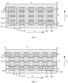
- FIG. 2 is a schematic top view of a structure of the solar cell according to an embodiment of the present disclosure.
- FIG. 3 is another schematic top view of a structure of the solar cell according to an embodiment of the present disclosure.
- FIG. 4 is yet another schematic top view of a structure of the solar cell according to an embodiment of the present disclosure.
- the electrodes and the passivation layers in FIGS. 2 to 4 are in a see-through state, that is, the surface of the doped conductive layer can be seen through the electrodes and the passivation layers.
- the solar cell includes: a substrate 100 including a doping element, the doping element is of N type or P type; a tunnel dielectric layer 120 located on a surface of the substrate 100; a doped conductive layer 121 located on a surface of the tunnel dielectric layer 120 away from the substrate 100, the doped conductive layer 121 includes a doping element of a type same as a type of the doping element of the substrate, and the doped conductive layer 121 includes a plurality of arrays 130 of heavily doped areas extending in a first direction X, the plurality of arrays 130 of heavily doped areas includes first heavily doped sub-areas 141 arranged at intervals in a second direction Y and second heavily doped sub-areas 142 arranged at intervals in the second direction; and a plurality of electrodes 151 arranged at intervals, where the plurality of electrodes 151 extend in the second direction Y
- the solar cell is a tunnel oxide passivated contact (TOPCon) cell, which may include a double-sided tunnel oxide passivated contact cell or a single-sided tunnel oxide passivated contact cell. As shown in Figure 1 , the solar cell is a single-sided tunnel oxide passivated contact cell.
- TOPCon tunnel oxide passivated contact
- the substrate 100 is a region that absorbs incident photons to generate photo-generated carriers.
- the substrate 100 is a silicon substrate 100, which may include one or more of monocrystalline silicon, polycrystalline silicon, amorphous silicon or microcrystalline silicon.
- the material of the substrate 100 may also be Silicon carbide, organic materials or multicomponent compounds.
- the multicomponent compound may include, but is not limited to, materials such as perovskite, gallium arsenide, cadmium telluride, copper indium selenide and the like.
- the substrate 100 in the present disclosure is a substrate of monocrystalline silicon.
- the substrate 100 has a first surface 101 and a second surface 102 opposite to each other, the first surface 101 of the substrate 100 is referred to as a front surface, and the second surface 102 of the substrate 100 is referred to as a rear surface. Further, for a single-sided cell, the first surface 101 of the substrate 100 is a light-receiving surface, and the second surface 102 of the substrate 100 is a backlight surface; for a double-sided cell, both the first surface 101 and the second surface 102 can function as a light-receiving surface to absorb incident light. As shown in FIG.
- the first surface 101 of the solar cell is provided with an emitter 110, and the first surface 101 has a textured structure, and the second surface 102 of the solar cell is provided with a tunnel dielectric layer 120 and a doped conductive layer 121, namely the solar cell is a positive junction cell.
- the substrate 100 includes a doping element, the doping element is of N type or P type, where the element of N type may be a pentavalent element such as phosphorus (P), bismuth (Bi), antimony (Sb) or arsenic (As) or the like, and the element of P type may be a trivalent element such as boron (B), aluminum (Al), gallium (Ga) or indium (In) or the like.
- the doping element in the substrate is of P type.
- the doping element in the substrate is of N type.
- a conductivity type of the doping element in the substrate 100 is the same as the type of the doping element in the doped conductive layer 121, for example, the doping element in the substrate 100 is of N type, and the doping element in the doped conductive layer 121 is of N type.
- the solar cell includes: an emitter 110 located on a side on which the first surface 101 of the substrate 100 is located.
- the substrate 100 and the emitter 110 form a PN junction.
- the substrate 100 includes a N-type doping element
- the emitter 110 includes a P-type doping element.
- the emitter 110 may be regarded as a part of the substrate 100, or, in other words, as an extension of the substrate 100.
- the emitter 110 can be arranged to have a pyramidal and textured surface, so as to reduce reflection of light on the surface of the emitter 110, thereby increasing the absorption and utilization rate of light, and improving the conversion efficiency of the solar cell.
- the tunnel dielectric layer 120 and the doped conductive layer 121 are located on a side where the second surface 102 of the substrate 100 is located.
- the tunnel dielectric layer 120 reduces the interface state density between the substrate 100 and the doped conductive layer 121 through chemical passivation, thereby reducing the recombination of minority carriers and holes, and being beneficial to reduce the Jo load current.
- the tunnel dielectric layer 120 allows majority carriers to tunnel into the doped conductive layer 121, and then the majority carriers are transported laterally in the doped conductive layer 121 and collected by the electrode 151, thereby greatly reducing the contact recombination current between the electrode 151 and the doped conductive layer 121, and improving open circuit voltage and short circuit current of the solar cell.
- material of the tunnel dielectric layer 120 may include, but is not limited to, dielectric materials with tunneling effect such as silicon oxide, silicon nitride, silicon oxynitride, intrinsic amorphous silicon, or intrinsic polysilicon or the like.
- a thickness of the tunnel dielectric layer 120 may be 0.5 nm to 3 nm, optionally, the thickness of the tunnel dielectric layer 120 is 0.5 nm to 2 nm, and further, the thickness of the tunnel dielectric layer 120 is 0.5 nm to 1.5 nm.
- Material of the doped conductive layer 121 can be at least one of polycrystalline semiconductor, amorphous semiconductor, microcrystalline semiconductor and single crystal semiconductor.
- the material of the doped conductive layer includes at least one of polycrystalline silicon, amorphous silicon and microcrystalline silicon.
- the thickness of the doped conductive layer 121 ranges from 20 nm to 150 nm.
- the thickness of the doped conductive layer 121 ranges from 60 nm to 90 nm.
- the above-mentioned ranges of thickness of the doped conductive layer 121 can ensure a low optical loss of the doped conductive layer 121 and a good interface passivation effect of the tunnel dielectric layer, thereby improving the efficiency of the cell.
- the material of the doped conductive layer 121 in the present disclosure is polysilicon, and the thickness of the doped conductive layer 121 is 80 nm.
- the plurality of arrays 130 of heavily doped areas can be regarded as locally heavily doped areas formed in the doped conductive layer 121, the plurality of arrays 130 of heavily doped areas are arranged at intervals in the second direction Y.
- the plurality of arrays 130 of heavily doped areas corresponds to positions of the orthographic projection of the electrodes 151 on the doped conductive layer 121, and the electrodes 151 contact with at least part of the plurality of arrays 130 of heavily doped areas of the doped conductive layer 121 to form an electrical connection.
- the formed plurality of arrays 130 of heavily doped areas are used to increase a number of majority carriers, and reduce the contact recombination current between the electrodes 151 and the doped conductive layer 121, thereby improving the photoelectric conversion efficiency of the solar cell.
- the arrays 130 of heavily doped areas located under a same electrode 151 are arranged at equal intervals, in this way, the current collection of each of the plurality of arrays 130 of heavily doped areas can be more uniform.
- a range of a width M of an array 130 of heavily doped areas in the first direction is N ⁇ M ⁇ 2N, where N represents a width of an electrode 151.
- the width of an array 130 of heavily doped areas is greater than the width of an electrode 151, to ensure that the areas being in contact with the electrodes 151 all belong to the plurality of arrays 130 of heavily doped areas, thereby reducing the contact resistance between the electrodes 151 and the doped conductive layer 121.
- the width of an array 130 of heavily doped areas is less than twice the width of an electrode 151, to ensure the field passivation effect of the doped conductive layer 121 not being in contact with the electrodes 151, and to prevent the areas occupied by the plurality of arrays 130 of heavily doped areas from being too large to cause recombination of majority carriers on surface of the substrate 100.
- the range of the width M of an array 130 of heavily doped areas is N ⁇ M ⁇ S1.2N.
- the electrodes 151 are, in a direction perpendicular to the surface of the substrate 100, in a form of a trapezoid with a narrow top and a wide bottom.
- a width of a top end of an electrode 151 is generally defined as the width of the electrode, so an actual width of a contact surface between an electrode 151 and the doped conductive layer 121 is greater than the width of the electrode.
- the width of an electrode 151 is an actual width of the contact surface between the electrode 151 and the doped conductive layer 121.
- the width of the contact surface between an electrode 151 and the doped conductive layer 121 ranges from 60 ⁇ m to 80 ⁇ m, that is, the width N of the electrode 151 is 60 ⁇ m to 80 ⁇ m, and the width M of an array 130 of heavily doped areas ranges from 60 ⁇ m to 110 ⁇ m, where the width M may be 60 ⁇ m, 80 ⁇ m, 90 ⁇ m or 103 ⁇ m.
- the first heavily doped sub-areas 141 are areas on which the doping treatment is performed, and the second heavily doped sub-areas 142 are areas formed by diffusion of the first heavily doped sub-areas 141.
- the doping concentration of the first heavily doped sub-areas 141 is greater than or equal to the doping concentration of the second heavily doped sub-areas 142, and as shown in FIG. 2 , the second heavily doped sub-areas 142 surround the first heavily doped sub-areas 141.
- the process parameters of the doping treatment can be controlled to make a spacing between the adjacent second heavily doped sub-areas 142 to be small or make a width of a formed overlapping area to be small. In this way, the contact area between an electrode 151 and an array 130 of heavily doped areas can be large, and the damage to the surface of the doped conductive layer 121 caused by the doping treatment can be small.
- the doping treatment is for example a laser doping treatment
- the number of light spots formed by the laser doping treatment per unit area is reduced, a larger number of solar cells can be subjected to the laser doping treatment per unit time, which is beneficial to improve the productivity of the solar cells.
- a range of a spacing P between adjacent first heavily doped sub-areas 141 in the second direction Y is 0.2O ⁇ P ⁇ 0.05O, where O represents a length of a first heavily doped sub-area 141.
- the spacing P between the first heavily doped sub-areas 141 is used to ensure sizes of the formed second heavily doped sub-areas 142, so that the spacing or the overlapping areas between the second heavily doped sub-areas 142 in adjacent arrays 130 of heavily doped areas are small, and the lengths of the first heavily doped sub-areas 141 are long.
- the length O of a first heavily doped sub-area 141 may range from 1 ⁇ m to 20 ⁇ m, and as an example, the length O of the first heavily doped sub-area 141 may be 1 ⁇ m, 6 ⁇ m, 13 ⁇ m or 18 ⁇ m.
- the spacing P between adjacent first heavily doped sub-areas 141 ranges from 2 ⁇ m to 10 ⁇ m. As an example, the spacing P between adjacent first heavily doped sub-areas 141 may be 3 ⁇ m, 5 ⁇ m, 8 ⁇ m or 9.3 ⁇ m.
- a range of the spacing P between adjacent first heavily doped sub-areas 141 in the second direction Y is 0.00006L ⁇ P ⁇ 0.00001L, where L represents a length of an electrode.
- each of the plurality of arrays 130 of heavily doped areas includes a plurality of sub-arrays 133 of doped areas arranged in the first direction X, and each of the plurality of sub-arrays 133 of doped areas includes a first heavily doped sub-area 141 and a second heavily doped sub-area 142. Since the diffusion is isotropic, each of the plurality of arrays 130 of heavily doped areas is divided into the plurality of sub-arrays 133 of doped areas, thereby further reducing the area on which the doping treatment is performed, which is beneficial to improve the productivity and reduce the damage area of the surface of the doped conductive layer 121. In this way, a high contact resistance generated when the electrodes are in contact with the damaged layer on the surface of the doped conductive layer 121 can be avoided, which is beneficial to improve the photoelectric conversion efficiency of the solar cells.
- a width W of a sub-array 133 of doped areas may be the width of a first heavily doped sub-area 141, and a range of the width W of the first heavily doped sub-area 141 of the sub-array 133 of doped areas in the first direction X is 0.1N ⁇ W ⁇ 1.2N, to ensure that in the first direction X, a distance between adjacent second heavily doped sub-areas 142 is small or an overlapping area between adjacent second heavily doped sub-areas 142 is small. In this way, the doping uniformity and the doping productivity of the plurality of arrays 130 of heavily doped areas can be improved.
- a range of the width W of a first heavily doped sub-area 141 of a sub-array 133 of doped areas is 10 ⁇ m ⁇ W ⁇ 110 ⁇ m, and as an example, the width W may be 10 ⁇ m, 39 ⁇ m, 63 ⁇ m or 101 ⁇ m.
- the width W of a first heavily doped sub-area 141 of a sub-array 133 of doped areas ranges from 15 ⁇ m to 40 ⁇ m, and the width W for example may be 15 ⁇ m, 25 ⁇ m, 31 ⁇ m or 40 ⁇ m.
- a range of a spacing U between adjacent sub-arrays 133 of doped areas is 2 ⁇ m ⁇ U ⁇ 10 ⁇ m, and as an example, the spacing U between adjacent sub-arrays 133 of doped areas may be 2.5 ⁇ m, 4.8 ⁇ m, 7.3 ⁇ m or 9.7 ⁇ m.
- At least two sub-arrays 133 of doped areas are arranged to be misaligned in the first direction X.
- the first heavily doped sub-areas 141 located in different sub-arrays 133 of doped areas are arranged to be misaligned, and the spacing between adjacent first heavily doped sub-areas 141 can be surrounded by the second heavily doped sub-areas 142 formed by diffusion in four directions, thereby reducing area of the blank areas (i.e. areas without heavy doping).
- the proportion of heavily doped areas in the surface where the electrodes and the doped conductive layer are in contact can be increased as much as possible.
- the contact resistance can be reduced, which is beneficial to improve the photoelectric conversion efficiency of the solar cells.
- a doping depth of the plurality of arrays 130 of heavily doped areas is less than or equal to a thickness of the doped conductive layer, which is beneficial to avoid damaging the surface of the tunnel dielectric layer 120 when forming the plurality of arrays 130 of heavily doped areas, and to avoid affecting the film uniformity of the tunnel dielectric layer 120, thereby affecting the effect of field passivation.
- each of the plurality of arrays 130 of heavily doped areas includes a first area 131 and a second area 132 arranged in the direction perpendicular to the substrate 100, a doping concentration of the second area 132 is smaller than a doping concentration of the first area 131, and each of the plurality of electrodes 151 is in contact with the first area 131 of the doped conductive layer 121.
- the first area 131 may include the first heavily doped sub-area 141 and the second heavily doped sub-area 142. In some other embodiments, the first area may include the first heavily doped sub-area.
- the cross-sectional shape of the second area 132 in the first direction X is a circular arc shape, a semicircular shape, an approximate circular arcs shape or an approximate semicircular shape.
- the cross-sectional shape of the second region 132 in the second direction Y is a circular arc shape, a semicircular shape, a concentric circular arc shape or an approximate semicircular shape.
- the doping concentration of the second area 132 is greater than or equal to the doping concentration of the doped conductive layer 121.
- the doping concentration of the second area 132 decreases in a gradient in a direction from the first area 131 to the second area 132, that is, the doping concentration of the second area 132 may be distributed in steps or a gradient in the direction from the first area 131 towards the second area 132, and the closer to the tunnel dielectric layer 120, the smaller the doping concentration.
- the solar cell further includes a passivation layer (not shown), the passivation layer is located on the surface of the doped conductive layer 121, and the plurality of electrodes 151 penetrate the passivation layer and contact with the surface the doped conductive layer 121.
- the passivation layer can reduce the recombination on the metal areas resulted from the contact of the electrodes 151 with the doped conductive layer 121, thereby improving efficiency of the cell.
- the passivation layer can be a single-layer structure or a laminated structure, and material of the passivation layer can be one or more of the materials such as silicon oxide, silicon nitride, silicon oxynitride, silicon oxycarbonitride, titanium oxide, hafnium oxide and aluminum oxide and the like.
- the passivation layer also has the function of an anti-reflection layer to increase light utilization.
- Each of the plurality of electrodes 151 functions as a grid line of the solar cell for collecting and converging the currents of the solar cell.
- the electrodes 151 may be sintered from a firing-through paste.
- the contact between the electrodes 151 and the doped conductive layer 121 may be a local contact or a complete contact.
- the material of the electrodes 151 may be one or more of aluminum, silver, gold, nickel, molybdenum and copper.
- the electrodes 151 are lower electrodes or back electrodes.
- the electrodes 151 refer to thin grid lines or finger-shaped grid lines to distinguish them from main grid lines or bus bars.
- the solar cell further includes: a first passivation layer 111, the first passivation layer 111 is located on the surface of the emitter 110 away from the substrate 100, and the first passivation layer 111 is regarded as a front passivation layer; and a plurality of first electrodes 152 arranged at intervals, the plurality of first electrodes 152 extend in the second direction Y, and the plurality of first electrodes 152 penetrate through the first passivation layer 111 and are in contact with the emitter 110.
- the first passivation layer 111 is a single-layer structure or a laminated structure, and the material of the first passivation layer 111 can be one or more of the materials such as silicon oxide, silicon nitride, silicon oxynitride, silicon oxycarbonitride, titanium oxide, hafnium oxide and aluminum oxide and the like.
- the plurality of first electrodes 152 may be sintered from a firing-through paste.
- the contact between the plurality of first electrodes 152 and the emitter 110 may be a local contact or a complete contact.
- the material of the plurality of first electrodes 152 may be one or more of aluminum, silver, gold, nickel, molybdenum and copper.
- the plurality of first electrodes 152 are upper electrodes or front electrodes. In some cases, the plurality of first electrodes 152 refer to thin grid lines or finger-shaped grid lines to distinguish them from main grid lines or bus bars.
- the doped conductive layer 121 includes the plurality of arrays 130 of locally and heavily doped areas extending in the first direction X, the doped conductive layer 121 can form obvious energy band bending on the surface of the substrate 100, thereby realizing a field passivation for minority carriers and a selective transport for majority carriers, and a good ohmic contact can be formed between the doped conductive layer and the electrodes 151 to ensure an effective transport of majority carriers.
- the plurality of electrodes 151 correspond to the plurality of arrays 130 of heavily doped areas, that is, a local doping treatment is performed on the regions where the plurality of arrays 130 of heavily doped areas are formed to reduce the damage contact area of the doped conductive layer 121, so that a good field passivation is formed by the tunnel dielectric layer 120 and the doped conductive layer 121. In this way, a carrier recombination rate on the surface can be reduced, and the photoelectric conversion efficiency of the cell can be improved.
- the entire area for the plurality of arrays 130 of heavily doped areas is divided into a plurality of first heavily doped sub-areas 141, that is, the areas on which the heavy doping treatment is performed are reduced, in this way, doping productivity can be improved.
- the entire heavily doped area is divided into a plurality of first heavily doped sub-areas 141 to avoid overlapping areas within the plurality of arrays 130 of heavily doped areas, in this way, a doping homogeneity and therefore the photoelectric conversion efficiency of the solar cell can be improved.
- FIG. 5 is a structural schematic diagram of a solar cell according to another embodiment of the present disclosure.
- a part of the solar cell as shown in FIG. 5 has the same structure as the solar cell as shown in FIGS. 1 to 4 , the main difference is that the tunnel dielectric layer and the doped conductive layer are located on the first surface (also called the front surface) of the substrate.
- the identical or similar contents or details of elements to those provided in the descriptions of the embodiments shown in FIGS. 1 to FIG. 4 will not be repeated, and only descriptions that are different from the above descriptions will be detailed.
- the solar cell provided by another embodiment of the present disclosure will be described in detail below with reference to FIG. 5 .
- the solar cell includes: a substrate 200 including a first surface 201 (also referred to as a front surface 201) and a second surface 202 (also referred to as a rear surface 202) opposite to the first surface; a tunnel dielectric layer 220 and a doped conductive layer 221 located on a side on which the first surface 201 of the substrate 200 is located, and the tunnel dielectric layer 220 is located between the doped conductive layer 221 and the substrate 200; a passivation layer 222, the passivation layer 222 is located on a surface of the doped conductive layer 221 away from the substrate 200, and the passivation layer 222 is regarded as a front passivation layer; a plurality of electrodes 251 (also referred to as first electrodes 251) arranged at intervals, the plurality of electrodes 251 extend in the second direction Y, and each of the plurality of electrodes 251 penetrates the passivation layer 222 and is in contact with at least part of the surface structures of
- the solar cell as shown in FIG. 5 may be a back junction solar cell, that is, the PN junction of the cell forms the back side of the cell.
- the doping element in the doped conductive layer 221 is of a type same as a type of the doping element of the substrate 200, for example, the substrate 200 is a N-type substrate, and the doped conductive layer 221 is doped with an N-type element; for another example, the substrate 200 is a P-type substrate, and the doped conductive layer 221 is doped with a P-type element.
- An emitter area is formed close to the second surface 202 and inside the substrate 200, the emitter area includes a doping element of a type opposite to that of the doping element of the substrate 200.
- the doped conductive layer 221 and the above-mentioned doped conductive layer 121 are the same or similar elements, that is, in some other embodiments of the present disclosure, the doped conductive layer 221 may include a plurality of arrays 230 of heavily doped areas extending in the first direction, each of the plurality of arrays 230 of heavily doped areas includes a first heavily doped sub-area 241 and a second heavily doped sub-area 242. Similarly, each of the plurality of arrays 230 of heavily doped areas may include a plurality of sub-arrays of doped areas arranged in the first direction.
- the second passivation layer is a single-layer structure or a laminated structure, and the material of the second passivation layer can be one or more of the materials such as silicon oxide, silicon nitride, silicon oxynitride, silicon oxycarbonitride, titanium oxide, hafnium oxide and aluminum oxide and the like.
- the electrode 252 may be sintered from a firing-through paste. The contact between the electrode 252 and the substrate 200 may be a local contact or a complete contact.
- the material of the electrode 252 may be one or more of aluminum, silver, gold, nickel, molybdenum and copper.
- the electrodes 251 are upper electrodes or front electrodes, and the electrode 252 are lower electrodes or back electrodes.
- the solar cell as shown in FIG. 1 or FIG. 5 is an example of providing a tunnel dielectric layer and a doped conductive layer with heavily doped areas on a single surface (the first surface or the second surface) of the substrate.
- Some other embodiments of the present disclosure further propose that both surfaces (the first surface and the second surface) of the substrate are respectively provided with a tunnel dielectric layer and a doped conductive layer, that is, the solar cell is a double-sided tunnel oxide passivated contact cell.
- FIG. 6 is a structural schematic diagram of a solar cell according to yet another embodiment of the present disclosure.
- the solar cell includes: a substrate 300 including a first surface 301 and a second surface 302 opposite to the first surface; a first tunnel dielectric layer 323, a first doped conductive layer 324, a third passivation layer 325 and an electrode 352 that are stacked in sequence and located on a side on which the first surface 301 of the substrate 300 is located, the electrode 352 penetrates the third passivation layer 325 and is in contact with the first doped conductive layer 324, the third passivation layer 325 is regarded as a front passivation layer, and the electrode 352 is an upper electrode or a front electrode; a tunnel dielectric layer 320 (also referred to as a second tunnel layer 320) and a doped conductive layer 321 (also referred to as a second conductive layer 321) located on a side on which the second surface 302 of the substrate 300 is located, and the tunnel dielectric
- the doping element of the first doped conductive layer 324 is of a type opposite to a type of the doping element in the substrate 300, and the doping element of the doped conductive layer 321 is of a type same as a type of the doping element in the substrate 300.
- the substrate 300 includes aN-type doping element
- the doped conductive layer 321 includes a N-type doping element
- the first doped conductive layer 324 includes a P-type doping element.
- the substrate 300 includes a P-type doping element
- the doped conductive layer 321 includes a P-type doping element
- the first doped conductive layer 324 includes a N-type doping element.
- the solar cell as shown in FIG. 6 may be a positive junction solar cell.
- the doped conductive layer 321 and the doped conductive layer 121 are the same or similar elements, that is, in some other embodiments of the present disclosure, the doped conductive layer 321 may include a plurality of arrays 330 of heavily doped areas extending in the first direction, each of the plurality of arrays 330 of heavily doped areas includes a first heavily doped sub-area 341 and a second heavily doped sub-area 342. Similarly, each of the plurality of arrays 330 of heavily doped areas may include a plurality of sub-arrays of doped areas arranged in the first direction.
- material of the first tunnel dielectric layer 323 may be any one of silicon oxide, silicon nitride, silicon oxynitride, intrinsic amorphous silicon and intrinsic polysilicon.
- the thickness of the first tunnel dielectric layer 323 may range from 0.5 nm to 3 nm. As an example, the thickness of the first tunnel dielectric layer 323 ranges from 0.5 nm to 2 nm, and further, the thickness of the first tunnel dielectric layer 323 ranges from 0.5 nm to 1.5 nm.
- the material of the first doped conductive layer 324 includes at least one of polysilicon, amorphous silicon and microcrystalline silicon. The thickness of the first doped conductive layer 324 ranges from 20 nm to 150 nm. As an example, the thickness of the first doped conductive layer 324 ranges from 60 nm to 90 nm.
- the third passivation layer 325 is a single-layer structure or a laminated structure, and the material of the third passivation layer 325 can be one or more of the materials such as silicon nitride, silicon oxynitride, silicon oxycarbonitride, titanium oxide, hafnium oxide and aluminum oxide and the like.
- the electrode 352 may be sintered from a firing-through paste.
- the contact between the electrode 352 and the first doped conductive layer 324 may be a local contact or a complete contact.
- the material of the electrode 352 may be one or more of aluminum, silver, gold, nickel, molybdenum and copper.
- FIG. 7 is a structural schematic diagram of a solar cell according to still another embodiment of the present disclosure.
- a part of the solar cell as shown in FIG. 7 has the same structure as the solar cell provided by the aforementioned embodiment ( FIG. 6 ).
- the identical or similar contents or details of elements to those provided in the descriptions of the above-mentioned embodiments will not be repeated, and only descriptions that are different from the above descriptions will be detailed.
- the solar cell includes: a substrate 400 including a first surface 401 and a second surface 402 opposite to the first surface; a tunnel dielectric layer 420 and a doped conductive layer 421 located on a side on which the first surface 401 of the substrate 400 is located, and the tunnel dielectric layer 420 is located between the doped conductive layer 421 and the substrate 400; a passivation layer 422, the passivation layer 422 is located on a surface of the doped conductive layer 421 away from the substrate 400, and the passivation layer 422 is regarded as a front passivation layer; a plurality of electrodes 451 arranged at intervals, the plurality of electrodes 451 extend in the second direction Y, and each of the plurality of electrodes 451 penetrates the passivation layer and is in contact with the doped conductive layer 421, the plurality of electrodes 451 are upper electrodes or front electrodes; a first tunnel dielectric layer 423 (also referred to as a first tunnel layer 423)
- the doped conductive layer 421 and the doped conductive layer 121 as shown in FIG. 1 to FIG. 4 are the same or similar elements, the doped conductive layer 421 may include a plurality of arrays 430 of heavily doped areas extending in the first direction, each of the plurality of arrays 430 of heavily doped areas includes a first heavily doped sub-area 441 and a second heavily doped sub-area 442. Similarly, each of the plurality of arrays 430 of heavily doped areas may include a plurality of sub-arrays of doped areas arranged in the first direction.
- the doping element of the doped conductive layer 421 is of a type same as a type of the doping element in the substrate 400, and the doping element of the first doped conductive layer 424 is of a type opposite to a type of the doping element in the substrate 400.
- the substrate 400 includes a N-type doping element
- the doped conductive layer 421 includes a N-type doping element
- the first doped conductive layer 424 includes a P-type doping element.
- the substrate 400 includes a P-type doping element
- the doped conductive layer 421 includes a P-type doping element
- the first doped conductive layer 424 includes a N-type doping element.
- the solar cell as shown in FIG. 7 may be a back junction solar cell.
- FIG. 8 is a structural schematic diagram of the photovoltaic module according to an embodiment of the present disclosure.
- the photovoltaic module includes: at least one cell string 10 formed by a plurality of solar cells provided by any one of the above embodiments ( FIGS. 1 to 7 ); an encapsulation adhesive film 21 used for covering a surface of the at least one cell string 10; and a cover plate 22 used for covering a surface of the encapsulation adhesive film 21 facing away from the at least one cell string 10.
- the encapsulation adhesive film 21 may be an organic encapsulation adhesive film such as EVA or POE and the like.
- the encapsulation adhesive film 21 covers the surfaces of the cell string 10 to seal and protect the cell string.
- the encapsulation adhesive film 21 may include an upper encapsulation adhesive film and a lower encapsulation adhesive film for encapsulating the upper and lower surfaces of the cell strings 10, respectively.
- the cover plate 22 can be a cover plate for protecting the cell string 10 such as a glass cover plate or a plastic cover plate.
- the cover plate 22 covers a surface of the encapsulation adhesive film 21 away from the cell string 10, and the cover plate 22 includes an upper cover plate located on a surface of the upper encapsulation adhesive film and a lower cover plate located on a surface of the lower encapsulation adhesive film.
- a light trapping structure is provided on the cover plate 22 to increase the utilization rate of incident light.
- the photovoltaic module has a high current collection capability and a low carrier recombination rate, which can achieve high photoelectric conversion efficiency.
- embodiments of the present disclosure further provide a production method for a solar cell, the method is used to produce the solar cell provided by the above embodiments (shown in FIGS. 1 to 4 ).
- the identical or similar contents or details of elements to those provided in the descriptions of the above embodiments will not be repeated, and only descriptions that are different from the above descriptions will be detailed.
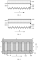
- FIGS. 9 to 21 are structural schematic diagrams corresponding to the operations of the production method for a solar cell according to an embodiment of the present disclosure.
- FIG. 13 , FIG. 14 , FIG. 15 and FIG. 18 are schematic top view of structures of the solar cell.
- a substrate 100 including a doping element is provided.
- the substrate 100 has a first surface 101 and a second surface 102 opposite to each other.
- the first surface 101 of the substrate 100 is a light-receiving surface
- the second surface 102 of the substrate 100 is a backlight surface.
- the first surface 101 of the substrate 100 has a textured structure
- the second surface 102 of the substrate 100 has a polished structure.
- an emitter 110 is formed, the emitter 110 is the first surface 101 of the substrate 100.
- a tunnel dielectric layer 120 is formed, the tunnel dielectric layer 120 is located on a surface of the substrate 100. As an example, the tunnel dielectric layer 120 is located on the second surface 102 of the substrate 100.
- a doped conductive layer 121 is formed, the doped conductive layer 121 is located on a surface of the tunnel dielectric layer 120 away from the substrate 100, the doped conductive layer 121 includes a doping element of a type same as a type of the doping element of the substrate 100, and the doped conductive layer 121 includes a plurality of arrays 130 of heavily doped areas extending in a first direction, the plurality of arrays 130 of heavily doped areas include first heavily doped sub-areas 141 arranged at intervals in a second direction Y and second heavily doped sub-areas 142 arranged at intervals in the second direction.
- a doped conductive film 103 is formed, the doped conductive film 103 is located on the surface of the tunnel dielectric layer 120 away from the substrate 100.
- an intrinsic doped conductive layer may be formed by low pressure chemical vapor deposition (LPCVD) and then a diffusion or an ion implantation doping is performed to form the doped conductive film 103, and the intrinsic doped conductive layer may be an intrinsic polysilicon layer.
- an initial conductive film is doped and deposited by plasma enhanced chemical vapor deposition (PECVD), and then is annealed to form the doped conductive film 103.
- the material of the initial conductive film may be amorphous silicon or microcrystalline silicon.
- the material of the doped conductive film 103 may be polycrystalline silicon, amorphous silicon, microcrystalline silicon or single crystal silicon. Exemplarily, the material of the doped conductive film 103 in the embodiments of the present disclosure is polysilicon.
- a first doping treatment is performed on the doped conductive film 103, the first doping treatment is used to perform doping treatment on the entire surface of the doped conductive film 103 to form areas of the doped conductive layer excluding the arrays of heavily doped areas.
- a dopant source layer 104 is formed on the surface of the doped conductive film 103, and a second doping treatment is performed on the doped conductive film 103 to form the doped conductive layer 121.
- the second doping treatment is used to form the arrays 130 of heavily doped areas, and after forming the doped conductive layer 121, the remaining dopant source layer 104 is removed.
- the dopant source layer 104 is located on the entire surface of the doped conductive film 103.
- the material of the dopant source layer 104 may include, but is not limited to, phosphosilicate glass (PSG) or borophosphosilicate glass (BPSG). In some other embodiments, the material of the dopant source layer may be borosilicate glass (BSG).
- the second doping treatment is laser doping.
- a light spot pattern 105 is formed by laser doping on a surface of the dopant source layer 104.
- a width A of the light spot pattern 105 is smaller than a width of an array of heavily doped areas which is subsequently formed, a length B of the light spot pattern 105 is equal to a length of a first heavily doped sub-area which is subsequently formed, and an interval C between adjacent light spot patterns 105 is equal to a length of the first heavily doped sub-area.
- the areas where the light spot patterns 105 are located are the areas for the first heavily doped sub-areas formed subsequently, so the specification parameters (width, length and interval, etc.) of the light spot pattern 105 are used to ensure that the effect achieved by the first heavily doped sub-areas formed subsequently, that is, the effect of the specification parameter ranges of the light spot pattern 105 is the same as the effect of the specification parameter ranges of the first heavily doped sub-areas, which will not be repeated here.
- the arrangement of the light spot patterns 105 in FIG. 14 can form the arrays of heavily doped areas as shown in FIG. 3 .
- a width E of a light spot pattern 105 in the first direction X is equal to the width W of a first heavily doped sub-area 141, and a spacing F between adjacent light spot patterns 105 in the first direction is equal to the spacing U between adj acent first heavily doped sub-areas 141;
- a length B of a light spot pattern 105 in the second direction Y is equal to a length O of a first heavily doped sub-area, and a spacing C between adjacent light spot patterns 105 in the second direction is equal to the spacing P between adjacent first heavily doped sub-areas 141.
- the arrangement of the light spot patterns 105 as shown in FIG. 15 is used to form the arrays of heavily doped areas as shown in FIG. 4 , and at least two columns of the light spot patterns 105 are arranged to be misaligned in the first direction X.
- a diffusion treatment is performed to diffuse the doping ions in part of the areas of the dopant source layer 104 (referring to FIG. 12 ) into the doped conductive film 103 (referring to FIG. 12 ) to form the arrays 130 of heavily doped areas. Then the dopant source layer 104 is removed.
- wet etching is used to completely remove the dopant source layer 104, so as to avoid the existence of residual phosphosilicate glass, which may cause surfaces of the silicon wafer to be wet in the air, resulting in the reduction of current and the attenuation of power.
- Complete removal of the dopant source layer also can prevent the passivation layer formed on the doped conductive layer 121 from peeling off, which is beneficial to improve the photoelectric conversion efficiency of the solar cell.
- the solution for the wet etching is a mixed liquid of HNO3 and HF.
- a thermal diffusion process or an ion implantation process may be used for the diffusion treatment.
- FIGS. 12-16 takes the example that the dopant source layer 104 is located on the entire surface of the doped conductive film 103, and a plurality of dopant source sub-layers distributed at intervals can also be formed in the embodiments of the present disclosure. The following will be described in detail with reference to FIG. 17 to FIG. 19 .
- a dopant source is formed on the surface of the doped conductive film 103.
- the dopant source includes a plurality of dopant source sub-layers 106, and the positions of the plurality of dopant source sub-layers 106 correspond to the positions of the first heavily doped sub-areas of the arrays of heavily doped areas.
- a width H of a dopant source sub-layer 106 is smaller than a width of a subsequently formed array of heavily doped area
- a length I of the dopant source sub-layer 106 is equal to a length of a subsequently formed first heavily doped sub-area
- a spacing G between adjacent dopant source sub-layers 106 is equal to the length of the first heavily doped sub-area.
- the areas where the dopant source sub-layers 106 are located are the areas for the first heavily doped sub-areas formed subsequently, so the specification parameters (width, length and spacing, etc.) of the dopant source sub-layers 106 are used to ensure that the effect achieved by the first heavily doped sub-areas formed subsequently, that is, the effect of the specification parameter ranges of the dopant source sub-layers 106 is the same as the effect of the specification parameter ranges of the first heavily doped sub-areas, which will not be repeated here.
- the arrangement of the dopant source sub-layers can form the arrays of heavily doped areas as shown in FIG. 3 .
- a width of a dopant source sub-layer in the first direction is equal to the width W of a first heavily doped sub-area 141, and a spacing between adjacent dopant source sub-layers in the first direction is equal to the spacing U between adjacent first heavily doped sub-areas 141;
- a length B of a dopant source sub-layer in the second direction Y is equal to a length O of a first heavily doped sub-area, and a spacing between adjacent dopant source sub-layers in the second direction is equal to the spacing P between adjacent first heavily doped sub-areas 141.
- the arrangement of the dopant source sub-layers can form the arrays of heavily doped areas as shown in FIG. 4 , and at least two columns of the dopant source sub-layers are arranged to be misaligned in the first direction X.
- the material of the dopant source sub-layers 106 may include, but is not limited to, phosphosilicate glass or borophosphosilicate glass.
- a diffusion treatment is performed to diffuse the doping element in the dopant source sub-layers 106 (referring to FIG. 17 ) into the doped conductive film 103 to form the arrays 130 of heavily doped areas. Then the dopant source sub-layers 106 are removed.
- the solar cell as shown in FIG. 16 and FIG. 19 can be formed by using a nanosecond laser with a laser wavelength of 532 nm or other lasers that can realize doping.
- the process parameters of the laser include: the laser frequency is 220kHz to 380kHz; the laser energy density is 0.1J/cm2 to 0.2J/cm2; the laser line scan speed is 20m/s to 35m/s.
- the process parameters of the diffusion treatment used for forming the solar cells as shown in FIGS. 16 and 19 may be different.
- the laser frequency is 220kHz to 350kHz
- the laser energy density is 0.15J/cm2 to 0.2J/cm2
- the laser line scan speed is 26m/s to 35m/s
- the width of the laser light spot is 80 ⁇ m to 110 ⁇ m.
- the process parameters for forming the solar cell as shown in FIG. 19 include: the laser frequency is 280kHz to 380kHz, the laser energy density is 0.1J/cm2 to 0.15J/cm2, the laser line scan speed is 20m/s to 28m/s, and the width of the laser light spot is 20 ⁇ m to 60 ⁇ m.
- a passivation layer 123 and a first passivation layer 111 are formed, the passivation layer 123 is located on the surface of the doped conductive layer 121 away from the substrate 100, and the first passivation layer 111 is located on the surface of the emitter 110.
- the passivation layer 123 is regarded as a rear passivation layer, and the first passivation layer 111 is regarded as a front passivation layer.
- the passivation layer 123 and the first passivation layer 111 also function as anti-reflection layers to increase light utilization.
- a plurality of electrodes 151 arranged at intervals are formed, the plurality of electrodes 151 extend in the second direction Y, and each of the plurality of electrodes 151 corresponds to an array 130 of heavily doped areas and is in contact with at least part of the surface structures of the plurality of arrays 130 of heavily doped areas of the doped conductive layer 121.
- the plurality of electrodes 151 are regarded as lower electrodes or back electrodes.
- a plurality of first electrodes 152 arranged at intervals are formed, the plurality of first electrodes 152 extend in the second direction Y, and each of the plurality of first electrodes 152 penetrates the first passivation layer 111 and is in contact with the emitter 110.
- the plurality of first electrodes 152 are regarded as upper electrodes or front electrodes.
- the production method for a solar cell can be used to form the solar cell as shown in FIG. 5 , the method includes: providing the substrate 200 including a first surface 201 and a second surface 202 opposite to the first surface; forming, in sequence, the tunnel dielectric layer 220, the doped conductive layer 221, the passivation layer 222 and the plurality of electrodes 251 arranged at intervals, where the tunnel dielectric layer 220, the doped conductive layer 221, the passivation layer 222 and the plurality of electrodes 251 are stacked and located on a side on which the first surface 201 is located, and the plurality of electrodes 251 penetrate the passivation layer 222 and are in contact with the doped conductive layer 221; and forming, in sequence, the second passivation layer and the electrodes 252 located on a side on which the second surface 202 is located, the electrodes 252 penetrates the second passivation layer and is in contact with the substrate 200.
- the process steps for forming the second passivation layer are the same as or similar to the process steps for forming the first passivation layer 111 (referring to FIG. 20 ) in the above-mentioned embodiments, and will not be repeated here.
- the process steps for forming the electrode 252 are the same as or similar to the process steps for forming the electrode 151 (referring to FIG. 21 ) in the above-mentioned embodiments.
- the production method for a solar cell can be used to form the solar cell as shown in FIG. 6 , the method includes: providing the substrate 300 including a first surface 301 and a second surface 302 opposite to the first surface; forming, in sequence, the first tunnel dielectric layer 323, the first doped conductive layer 324, the third passivation layer 325 and the electrode 352 that are stacked and located on a side on which the first surface 301 is located, where the electrode 352 penetrates the third passivation layer 325 and is in contact with the first doped conductive layer 324; and forming, in sequence, the tunnel dielectric layer 320, the doped conductive layer 321, the passivation layer and the plurality of electrodes 351 arranged at intervals, where the tunnel dielectric layer 320, the doped conductive layer 321, the passivation layer and the plurality of electrodes 351 are stacked and located on a side on which the second surface 302 is located, and the plurality of electrodes 351 penetrate the passivation layer and are
- the process steps for forming the first tunnel dielectric layer 323 are the same as or similar to the process steps for forming the tunnel dielectric layer 120 (referring to FIG. 11 ) in the above-mentioned embodiments, and will not be repeated here.
- the process steps for forming the first doped conductive layer 324 are the same as or similar to the process steps for forming the doped conductive film 103 (referring to FIG. 11 ) in the above-mentioned embodiments.
- the process steps for forming the third passivation layer 325 are the same as or similar to the process steps for forming the passivation layer (referring to FIG. 20 ) in the above-mentioned embodiments.
- the process steps for forming the electrode 352 are the same as or similar to the process steps for forming the electrode 151 (referring to FIG. 21 ) in the above-mentioned embodiments.
- the production method for a solar cell can be used to form the solar cell as shown in FIG. 7 , the method includes: providing the substrate 400 including the first surface 401 and the second surface 402 opposite to the first surface; forming, in sequence, the tunnel dielectric layer 420, the doped conductive layer 421, the passivation layer 422 and the plurality of electrodes 451 arranged at intervals, where the tunnel dielectric layer 420, the doped conductive layer 421, the passivation layer 422 and the plurality of electrodes 451 are stacked and located on a side on which the first surface 401 is located, and the plurality of electrodes 451 penetrate the passivation layer 422 and are in contact with the doped conductive layer 421; and forming, in sequence, the first tunnel dielectric layer 423, the first doped conductive layer 424, the third passivation layer and the electrode 452 that are stacked and located on a side on which the second surface 402 is located, the electrode 452 penetrates the third passivation layer and is in
Landscapes
- Photovoltaic Devices (AREA)
- Life Sciences & Earth Sciences (AREA)
- Engineering & Computer Science (AREA)
- Sustainable Development (AREA)
- Sustainable Energy (AREA)
Abstract
Embodiments of the present disclosure provide a solar cell and a production method thereof, and a photovoltaic module. The solar cell includes: a substrate; a tunnel dielectric layer, located on a surface of the substrate; a doped conductive layer, located on a surface of the tunnel dielectric layer away from the substrate, the doped conductive layer includes a doping element of a same type as a doping element of the substrate, and a plurality of arrays of heavily doped areas extending in a first direction, the arrays includes first heavily doped sub-areas and second heavily doped sub-areas arranged at intervals in a second direction; and a plurality of electrodes arranged at intervals, the electrodes extend in the second direction and correspond to the arrays, and the electrodes contact with at least part of the arrays. The present disclosure can improve photoelectric conversion efficiency of the solar cell.
Description
- Embodiments of the present disclosure relates to the field of photovoltaics, and in particular to a solar cell and a production method for the solar cell, and a photovoltaic module.
- The reasons that affect performance of solar cells (such as photoelectric conversion efficiency) include optical losses and electrical losses. The optical losses include reflection loss on front surface of the cells, shadow loss due to contact with grid lines, and non-absorption loss in long-wavelength bands. The electrical losses include losses due to photo-generated carrier recombination on surface and in interior of semiconductor, contact resistance between semiconductor and metal grid ode and semiconductor and the like.
- For the purpose of reducing the electrical losses of the solar cells, a tunnel oxide passivated structure for metal contact is formed on the surface of the cells. The tunnel oxide passivated structure for metal contact includes an ultra-thin tunnel dielectric layer and a doped conductive layer. This structure can provide good surface passivation, thereby reducing recombination current at metal contact and improving open-circuit voltage and short-circuit current of the cells. The tunnel oxide passivated structure for metal contact can optimize performance of the solar cells, but there are still many factors that affect the performance of the solar cells of this type. It is of great significance to develop passivated contact solar cells with high efficiency.
- Embodiments of the present disclosure provide a solar cell and a production method thereof, and a photovoltaic module, which is at least beneficial to improve photoelectric conversion efficiency of a passivated contact solar cell.
- Some embodiments of the present disclosure provide a solar cell, including: a substrate including a doping element, where the doping element is of N type or P type; a tunnel dielectric layer located on a surface of the substrate; a doped conductive layer located on a surface of the tunnel dielectric layer away from the substrate, the doped conductive layer includes a doping element of a type same as a type of the doping element of the substrate, and the doped conductive layer includes a plurality of arrays of heavily doped areas extending in a first direction, the plurality of arrays of heavily doped areas includes first heavily doped sub-areas arranged at intervals in a second direction and second heavily doped sub-areas arranged at intervals in the second direction; and a plurality of electrodes arranged at intervals, where the plurality of electrodes extend in the second direction and correspond to the plurality of arrays of heavily doped areas, and the plurality of electrodes contact with at least part of the plurality of arrays of heavily doped areas of the doped conductive layer.
- Some embodiments of the present disclosure provide a photovoltaic module, including: at least one cell string formed by a plurality of solar cells according to any one of above-mentioned embodiments; an encapsulation adhesive film used for covering a surface of the at least one cell string; and a cover plate used for covering a surface of the encapsulation adhesive film facing away from the at least one cell string.
- Some embodiments of the present disclosure provide a production method for a solar cell, including: providing a substrate including a doping element; forming a tunnel dielectric layer located on a surface of the substrate; forming a doped conductive layer located on a surface of the tunnel dielectric layer away from the substrate, where the doped conductive layer includes a doping element of a type same as a type of the doping element of the substrate, and the doped conductive layer includes a plurality of arrays of heavily doped areas extending in a first direction, where the plurality of arrays of heavily doped areas includes first heavily doped sub-areas arranged at intervals in a second direction and second heavily doped sub-areas arranged at intervals in the second direction; and forming a plurality of electrodes arranged at intervals, where the plurality of electrodes extend in the second direction and correspond to the plurality of arrays of heavily doped areas, and where the plurality of electrodes contact with at least part of the plurality of arrays of heavily doped areas of the doped conductive layer.
- One or more embodiments are exemplarily illustrated in reference to corresponding accompanying drawing(s), and these exemplary illustrations do not constitute limitations on the embodiments. Unless otherwise stated, the accompanying drawings do not constitute scale limitations. In order to more clearly illustrate the embodiments of the present disclosure or the technical solutions in the prior art, the accompanying drawings used in the embodiments will be briefly described below. Obviously, the drawings in the following description are only some embodiments of the present disclosure. For those skilled in the art, other drawings can be obtained based on these drawings without any inventive works.
-
FIG. 1 is a structural schematic diagram of a solar cell according to an embodiment of the present disclosure. -
FIG. 2 is a schematic top view of a structure of the solar cell according to an embodiment of the present disclosure. -
FIG. 3 is another schematic top view of a structure of the solar cell according to an embodiment of the present disclosure. -
FIG. 4 is yet another schematic top view of a structure of the solar cell according to an embodiment of the present disclosure. -
FIG. 5 is a structural schematic diagram of a solar cell according to another embodiment of the present disclosure. -
FIG. 6 is a structural schematic diagram of a solar cell according to yet another embodiment of the present disclosure. -
FIG. 7 is a structural schematic diagram of a solar cell according to still another embodiment of the present disclosure. -
FIG. 8 is a structural schematic diagram of a photovoltaic module according to an embodiment of the present disclosure. -
FIGS. 9 to 21 are structural schematic diagrams corresponding to the operations of a production method for a solar cell according to an embodiment of the present disclosure. - It can be known from the background art that the existing passivated contact solar cells have a problem of low photoelectric conversion efficiency.
- By analysis, it is found that one of the reasons for the low photoelectric conversion efficiency of passivated contact solar cells is that in order to improve the photoelectric conversion efficiency of solar cells, local heavy doping treatment is performed on the doped conductive layer, and the formed heavily doped areas correspond to the positions of electrodes, thereby forming an entire heavily doped area. However, during for example laser doping, in order to form a continuous heavily doped area, consecutive laser spots are formed, that is, laser spots without gap therebetween are formed. Due to diffusion, multiple overlapping areas are formed in the heavily doped areas, leading to inhomogeneous doping concentration of the heavily doped areas (where the doping concentration of the overlapping areas is relatively high), thereby affecting the photoelectric conversion efficiency of the solar cells.
- Embodiments of the present disclosure provide a solar cell and a production method thereof, and a photovoltaic module. Each of the arrays of heavily doped areas in the doped conductive layer is divided into a plurality of first heavily doped sub-areas and a plurality of second heavily doped sub-areas, where the plurality of second heavily doped sub-areas are located at the peripheries of the plurality of first heavily doped sub-areas, and the plurality of second heavily doped sub-areas are formed by diffusion of the plurality of first heavily doped sub-areas. Thus, doping treatment can be performed only on the areas where the plurality of first heavily doped sub-areas are located, and there can be no overlapping area between adjacent second heavily doped sub-areas. In this way, the doping concentration can be relatively homogeneous, and the doping homogeneity and the photoelectric conversion efficiency of the solar cells can be improved. Moreover, the doping treated areas are relatively small, for example, in a same solar cell, a number of laser spots in the laser doping is reduced, thereby improving the doping productivity and reducing the damage contact area of the doped conductive layer. Furthermore, the doped conductive layer is provided with arrays of heavily doped areas, thus the arrays of heavily doped areas are in contact with electrodes and a good ohmic contact can be formed. In this way, an effective transport of majority carriers can be ensured, and the photoelectric conversion efficiency of the solar cells can be improved.
- Embodiments of the present disclosure will be described in detail below with reference to the accompanying drawings. Those skilled in the art should understand that, in the embodiments of the present disclosure, many technical details are provided for the reader to better understand the present disclosure. However, even without these technical details and various modifications and variants based on the following embodiments, the technical solutions claimed in the present disclosure can be realized.
-
FIG. 1 is a structural schematic diagram of a solar cell according to an embodiment of the present disclosure.FIG. 2 is a schematic top view of a structure of the solar cell according to an embodiment of the present disclosure.FIG. 3 is another schematic top view of a structure of the solar cell according to an embodiment of the present disclosure.FIG. 4 is yet another schematic top view of a structure of the solar cell according to an embodiment of the present disclosure. The electrodes and the passivation layers inFIGS. 2 to 4 are in a see-through state, that is, the surface of the doped conductive layer can be seen through the electrodes and the passivation layers. - Embodiments of the present disclosure provide, on one hand, a solar cell. As shown in
FIGS. 1 to 4 , the solar cell includes: asubstrate 100 including a doping element, the doping element is of N type or P type; a tunneldielectric layer 120 located on a surface of thesubstrate 100; a dopedconductive layer 121 located on a surface of the tunneldielectric layer 120 away from thesubstrate 100, the dopedconductive layer 121 includes a doping element of a type same as a type of the doping element of the substrate, and the dopedconductive layer 121 includes a plurality ofarrays 130 of heavily doped areas extending in a first direction X, the plurality ofarrays 130 of heavily doped areas includes first heavily dopedsub-areas 141 arranged at intervals in a second direction Y and second heavily dopedsub-areas 142 arranged at intervals in the second direction; and a plurality ofelectrodes 151 arranged at intervals, where the plurality ofelectrodes 151 extend in the second direction Y and correspond to the plurality ofarrays 130 of heavily doped areas, and the plurality ofelectrodes 151 contact with at least part of the plurality ofarrays 130 of heavily doped areas of the dopedconductive layer 121. - In some embodiments, the solar cell is a tunnel oxide passivated contact (TOPCon) cell, which may include a double-sided tunnel oxide passivated contact cell or a single-sided tunnel oxide passivated contact cell. As shown in
Figure 1 , the solar cell is a single-sided tunnel oxide passivated contact cell. - The
substrate 100 is a region that absorbs incident photons to generate photo-generated carriers. In some embodiments, thesubstrate 100 is asilicon substrate 100, which may include one or more of monocrystalline silicon, polycrystalline silicon, amorphous silicon or microcrystalline silicon. In some other embodiments, the material of thesubstrate 100 may also be Silicon carbide, organic materials or multicomponent compounds. The multicomponent compound may include, but is not limited to, materials such as perovskite, gallium arsenide, cadmium telluride, copper indium selenide and the like. As an example, thesubstrate 100 in the present disclosure is a substrate of monocrystalline silicon. - In some embodiments, the
substrate 100 has afirst surface 101 and asecond surface 102 opposite to each other, thefirst surface 101 of thesubstrate 100 is referred to as a front surface, and thesecond surface 102 of thesubstrate 100 is referred to as a rear surface. Further, for a single-sided cell, thefirst surface 101 of thesubstrate 100 is a light-receiving surface, and thesecond surface 102 of thesubstrate 100 is a backlight surface; for a double-sided cell, both thefirst surface 101 and thesecond surface 102 can function as a light-receiving surface to absorb incident light. As shown inFIG. 1 , thefirst surface 101 of the solar cell is provided with anemitter 110, and thefirst surface 101 has a textured structure, and thesecond surface 102 of the solar cell is provided with a tunneldielectric layer 120 and a dopedconductive layer 121, namely the solar cell is a positive junction cell. - In some embodiments, the
substrate 100 includes a doping element, the doping element is of N type or P type, where the element of N type may be a pentavalent element such as phosphorus (P), bismuth (Bi), antimony (Sb) or arsenic (As) or the like, and the element of P type may be a trivalent element such as boron (B), aluminum (Al), gallium (Ga) or indium (In) or the like. For example, when thesubstrate 100 is a substrate of P type, the doping element in the substrate is of P type. For another example, when thesubstrate 100 is a substrate of N type, the doping element in the substrate is of N type. - In some embodiments, a conductivity type of the doping element in the
substrate 100 is the same as the type of the doping element in the dopedconductive layer 121, for example, the doping element in thesubstrate 100 is of N type, and the doping element in the dopedconductive layer 121 is of N type. - In some embodiments, the solar cell includes: an
emitter 110 located on a side on which thefirst surface 101 of thesubstrate 100 is located. Thesubstrate 100 and theemitter 110 form a PN junction. For example, thesubstrate 100 includes a N-type doping element, and theemitter 110 includes a P-type doping element. In some other embodiments, theemitter 110 may be regarded as a part of thesubstrate 100, or, in other words, as an extension of thesubstrate 100. In addition, theemitter 110 can be arranged to have a pyramidal and textured surface, so as to reduce reflection of light on the surface of theemitter 110, thereby increasing the absorption and utilization rate of light, and improving the conversion efficiency of the solar cell. - In some embodiments, the
tunnel dielectric layer 120 and the dopedconductive layer 121 are located on a side where thesecond surface 102 of thesubstrate 100 is located. Thetunnel dielectric layer 120 reduces the interface state density between thesubstrate 100 and the dopedconductive layer 121 through chemical passivation, thereby reducing the recombination of minority carriers and holes, and being beneficial to reduce the Jo load current. Thetunnel dielectric layer 120 allows majority carriers to tunnel into the dopedconductive layer 121, and then the majority carriers are transported laterally in the dopedconductive layer 121 and collected by theelectrode 151, thereby greatly reducing the contact recombination current between theelectrode 151 and the dopedconductive layer 121, and improving open circuit voltage and short circuit current of the solar cell. - In some embodiments, material of the
tunnel dielectric layer 120 may include, but is not limited to, dielectric materials with tunneling effect such as silicon oxide, silicon nitride, silicon oxynitride, intrinsic amorphous silicon, or intrinsic polysilicon or the like. A thickness of thetunnel dielectric layer 120 may be 0.5 nm to 3 nm, optionally, the thickness of thetunnel dielectric layer 120 is 0.5 nm to 2 nm, and further, the thickness of thetunnel dielectric layer 120 is 0.5 nm to 1.5 nm. - Material of the doped
conductive layer 121 can be at least one of polycrystalline semiconductor, amorphous semiconductor, microcrystalline semiconductor and single crystal semiconductor. As an example, the material of the doped conductive layer includes at least one of polycrystalline silicon, amorphous silicon and microcrystalline silicon. The thickness of the dopedconductive layer 121 ranges from 20 nm to 150 nm. As an example, the thickness of the dopedconductive layer 121 ranges from 60 nm to 90 nm. The above-mentioned ranges of thickness of the dopedconductive layer 121 can ensure a low optical loss of the dopedconductive layer 121 and a good interface passivation effect of the tunnel dielectric layer, thereby improving the efficiency of the cell. As an example, the material of the dopedconductive layer 121 in the present disclosure is polysilicon, and the thickness of the dopedconductive layer 121 is 80 nm. - In some embodiments, the plurality of
arrays 130 of heavily doped areas can be regarded as locally heavily doped areas formed in the dopedconductive layer 121, the plurality ofarrays 130 of heavily doped areas are arranged at intervals in the second direction Y. The plurality ofarrays 130 of heavily doped areas corresponds to positions of the orthographic projection of theelectrodes 151 on the dopedconductive layer 121, and theelectrodes 151 contact with at least part of the plurality ofarrays 130 of heavily doped areas of the dopedconductive layer 121 to form an electrical connection. The formed plurality ofarrays 130 of heavily doped areas are used to increase a number of majority carriers, and reduce the contact recombination current between theelectrodes 151 and the dopedconductive layer 121, thereby improving the photoelectric conversion efficiency of the solar cell. Thearrays 130 of heavily doped areas located under asame electrode 151 are arranged at equal intervals, in this way, the current collection of each of the plurality ofarrays 130 of heavily doped areas can be more uniform. - In some embodiments, as shown in
FIG. 2 , a range of a width M of anarray 130 of heavily doped areas in the first direction is N≤M≤2N, where N represents a width of anelectrode 151. The width of anarray 130 of heavily doped areas is greater than the width of anelectrode 151, to ensure that the areas being in contact with theelectrodes 151 all belong to the plurality ofarrays 130 of heavily doped areas, thereby reducing the contact resistance between theelectrodes 151 and the dopedconductive layer 121. The width of anarray 130 of heavily doped areas is less than twice the width of anelectrode 151, to ensure the field passivation effect of the dopedconductive layer 121 not being in contact with theelectrodes 151, and to prevent the areas occupied by the plurality ofarrays 130 of heavily doped areas from being too large to cause recombination of majority carriers on surface of thesubstrate 100. As an example, the range of the width M of anarray 130 of heavily doped areas is N≤ M≤S1.2N. - It should be understood that the
electrodes 151 are, in a direction perpendicular to the surface of thesubstrate 100, in a form of a trapezoid with a narrow top and a wide bottom. In the art, a width of a top end of anelectrode 151 is generally defined as the width of the electrode, so an actual width of a contact surface between anelectrode 151 and the dopedconductive layer 121 is greater than the width of the electrode. In the embodiments of the present disclosure, the width of anelectrode 151 is an actual width of the contact surface between theelectrode 151 and the dopedconductive layer 121. As an example, the width of the contact surface between anelectrode 151 and the dopedconductive layer 121 ranges from 60 µm to 80 µm, that is, the width N of theelectrode 151 is 60 µm to 80 µm, and the width M of anarray 130 of heavily doped areas ranges from 60 µm to 110 µm, where the width M may be 60 µm, 80 µm, 90 µm or 103 µm. - In some embodiments, referring to
FIG. 1 , the first heavily doped sub-areas 141 are areas on which the doping treatment is performed, and the second heavily doped sub-areas 142 are areas formed by diffusion of the first heavily dopedsub-areas 141. The doping concentration of the first heavily doped sub-areas 141 is greater than or equal to the doping concentration of the second heavily doped sub-areas 142, and as shown inFIG. 2 , the second heavily doped sub-areas 142 surround the first heavily dopedsub-areas 141. - It should be understood that there is a blank heavily doped area (i.e. an area without heavy doping) between the adjacent second heavily doped sub-areas 142, as shown in
FIG. 1 , and the blank heavily doped area is schematically shown as an interval between the adjacent second heavily dopedsub-areas 142. In the actual process of producing the solar cell, the process parameters of the doping treatment can be controlled to make a spacing between the adjacent second heavily doped sub-areas 142 to be small or make a width of a formed overlapping area to be small. In this way, the contact area between anelectrode 151 and anarray 130 of heavily doped areas can be large, and the damage to the surface of the dopedconductive layer 121 caused by the doping treatment can be small. When the doping treatment is for example a laser doping treatment, since the number of light spots formed by the laser doping treatment per unit area is reduced, a larger number of solar cells can be subjected to the laser doping treatment per unit time, which is beneficial to improve the productivity of the solar cells. - In some embodiments, referring to
FIG. 2 , a range of a spacing P between adjacent first heavily doped sub-areas 141 in the second direction Y is 0.2O≥P≥0.05O, where O represents a length of a first heavily dopedsub-area 141. The spacing P between the first heavily doped sub-areas 141 is used to ensure sizes of the formed second heavily doped sub-areas 142, so that the spacing or the overlapping areas between the second heavily doped sub-areas 142 inadjacent arrays 130 of heavily doped areas are small, and the lengths of the first heavily doped sub-areas 141 are long. In this way, the contact area between the plurality of electrodes and the plurality ofarrays 130 of heavily doped areas can be large, which is beneficial to improve the photoelectric conversion efficiency of the solar cells. The length O of a first heavily dopedsub-area 141 may range from 1 µm to 20 µm, and as an example, the length O of the first heavily dopedsub-area 141 may be 1 µm, 6 µm, 13 µm or 18 µm. The spacing P between adjacent first heavily doped sub-areas 141 ranges from 2 µm to 10 µm. As an example, the spacing P between adjacent first heavily doped sub-areas 141 may be 3 µm, 5 µm, 8 µm or 9.3 µm. - In some embodiments, a range of the spacing P between adjacent first heavily doped sub-areas 141 in the second direction Y is 0.00006L≥P≥0.00001L, where L represents a length of an electrode.
- In some embodiments, as shown in
FIG. 3 , each of the plurality ofarrays 130 of heavily doped areas includes a plurality ofsub-arrays 133 of doped areas arranged in the first direction X, and each of the plurality ofsub-arrays 133 of doped areas includes a first heavily dopedsub-area 141 and a second heavily dopedsub-area 142. Since the diffusion is isotropic, each of the plurality ofarrays 130 of heavily doped areas is divided into the plurality ofsub-arrays 133 of doped areas, thereby further reducing the area on which the doping treatment is performed, which is beneficial to improve the productivity and reduce the damage area of the surface of the dopedconductive layer 121. In this way, a high contact resistance generated when the electrodes are in contact with the damaged layer on the surface of the dopedconductive layer 121 can be avoided, which is beneficial to improve the photoelectric conversion efficiency of the solar cells. - In some embodiments, a width W of a sub-array 133 of doped areas may be the width of a first heavily doped
sub-area 141, and a range of the width W of the first heavily dopedsub-area 141 of the sub-array 133 of doped areas in the first direction X is 0.1N≤W≤1.2N, to ensure that in the first direction X, a distance between adjacent second heavily doped sub-areas 142 is small or an overlapping area between adjacent second heavily doped sub-areas 142 is small. In this way, the doping uniformity and the doping productivity of the plurality ofarrays 130 of heavily doped areas can be improved. A range of the width W of a first heavily dopedsub-area 141 of a sub-array 133 of doped areas is 10 µm≤W≤110 µm, and as an example, the width W may be 10 µm, 39 µm, 63 µm or 101 µm. As an example, the width W of a first heavily dopedsub-area 141 of a sub-array 133 of doped areas ranges from 15 µm to 40 µm, and the width W for example may be 15 µm, 25 µm, 31 µm or 40 µm. A range of a spacing U betweenadjacent sub-arrays 133 of doped areas is 2 µm≤U≤10 µm, and as an example, the spacing U betweenadjacent sub-arrays 133 of doped areas may be 2.5 µm, 4.8 µm, 7.3 µm or 9.7 µm. - In some embodiments, as shown in
FIG. 4 , at least twosub-arrays 133 of doped areas are arranged to be misaligned in the first direction X. In the first direction X, the first heavily doped sub-areas 141 located indifferent sub-arrays 133 of doped areas are arranged to be misaligned, and the spacing between adjacent first heavily doped sub-areas 141 can be surrounded by the second heavily doped sub-areas 142 formed by diffusion in four directions, thereby reducing area of the blank areas (i.e. areas without heavy doping). In this way, the proportion of heavily doped areas in the surface where the electrodes and the doped conductive layer are in contact can be increased as much as possible. Thus, the contact resistance can be reduced, which is beneficial to improve the photoelectric conversion efficiency of the solar cells. - Referring to
FIG. 1 , in some embodiments, in a direction perpendicular to thesubstrate 100, a doping depth of the plurality ofarrays 130 of heavily doped areas is less than or equal to a thickness of the doped conductive layer, which is beneficial to avoid damaging the surface of thetunnel dielectric layer 120 when forming the plurality ofarrays 130 of heavily doped areas, and to avoid affecting the film uniformity of thetunnel dielectric layer 120, thereby affecting the effect of field passivation. - In some embodiments, each of the plurality of
arrays 130 of heavily doped areas includes afirst area 131 and asecond area 132 arranged in the direction perpendicular to thesubstrate 100, a doping concentration of thesecond area 132 is smaller than a doping concentration of thefirst area 131, and each of the plurality ofelectrodes 151 is in contact with thefirst area 131 of the dopedconductive layer 121. Thefirst area 131 may include the first heavily dopedsub-area 141 and the second heavily dopedsub-area 142. In some other embodiments, the first area may include the first heavily doped sub-area. - In some embodiments, due to the principle of diffusion, the cross-sectional shape of the
second area 132 in the first direction X is a circular arc shape, a semicircular shape, an approximate circular arcs shape or an approximate semicircular shape. Similarly, the cross-sectional shape of thesecond region 132 in the second direction Y is a circular arc shape, a semicircular shape, a concentric circular arc shape or an approximate semicircular shape. The doping concentration of thesecond area 132 is greater than or equal to the doping concentration of the dopedconductive layer 121. The doping concentration of thesecond area 132 decreases in a gradient in a direction from thefirst area 131 to thesecond area 132, that is, the doping concentration of thesecond area 132 may be distributed in steps or a gradient in the direction from thefirst area 131 towards thesecond area 132, and the closer to thetunnel dielectric layer 120, the smaller the doping concentration. - In some embodiments, referring to
FIG. 1 , the solar cell further includes a passivation layer (not shown), the passivation layer is located on the surface of the dopedconductive layer 121, and the plurality ofelectrodes 151 penetrate the passivation layer and contact with the surface the dopedconductive layer 121. The passivation layer can reduce the recombination on the metal areas resulted from the contact of theelectrodes 151 with the dopedconductive layer 121, thereby improving efficiency of the cell. The passivation layer can be a single-layer structure or a laminated structure, and material of the passivation layer can be one or more of the materials such as silicon oxide, silicon nitride, silicon oxynitride, silicon oxycarbonitride, titanium oxide, hafnium oxide and aluminum oxide and the like. For those skilled in the art, the passivation layer also has the function of an anti-reflection layer to increase light utilization. - Each of the plurality of
electrodes 151 functions as a grid line of the solar cell for collecting and converging the currents of the solar cell. Theelectrodes 151 may be sintered from a firing-through paste. The contact between theelectrodes 151 and the dopedconductive layer 121 may be a local contact or a complete contact. The material of theelectrodes 151 may be one or more of aluminum, silver, gold, nickel, molybdenum and copper. In some embodiments, as shown inFIG. 1 , when the dopedconductive layer 121 is located on the back surface of thesubstrate 100, theelectrodes 151 are lower electrodes or back electrodes. In some cases, theelectrodes 151 refer to thin grid lines or finger-shaped grid lines to distinguish them from main grid lines or bus bars. - In some embodiments, the solar cell further includes: a
first passivation layer 111, thefirst passivation layer 111 is located on the surface of theemitter 110 away from thesubstrate 100, and thefirst passivation layer 111 is regarded as a front passivation layer; and a plurality offirst electrodes 152 arranged at intervals, the plurality offirst electrodes 152 extend in the second direction Y, and the plurality offirst electrodes 152 penetrate through thefirst passivation layer 111 and are in contact with theemitter 110. - In some embodiments, the
first passivation layer 111 is a single-layer structure or a laminated structure, and the material of thefirst passivation layer 111 can be one or more of the materials such as silicon oxide, silicon nitride, silicon oxynitride, silicon oxycarbonitride, titanium oxide, hafnium oxide and aluminum oxide and the like. The plurality offirst electrodes 152 may be sintered from a firing-through paste. The contact between the plurality offirst electrodes 152 and theemitter 110 may be a local contact or a complete contact. The material of the plurality offirst electrodes 152 may be one or more of aluminum, silver, gold, nickel, molybdenum and copper. The plurality offirst electrodes 152 are upper electrodes or front electrodes. In some cases, the plurality offirst electrodes 152 refer to thin grid lines or finger-shaped grid lines to distinguish them from main grid lines or bus bars. - In the solar cell as shown in
FIGS. 1 and4 , the dopedconductive layer 121 includes the plurality ofarrays 130 of locally and heavily doped areas extending in the first direction X, the dopedconductive layer 121 can form obvious energy band bending on the surface of thesubstrate 100, thereby realizing a field passivation for minority carriers and a selective transport for majority carriers, and a good ohmic contact can be formed between the doped conductive layer and theelectrodes 151 to ensure an effective transport of majority carriers. Moreover, the plurality ofelectrodes 151 correspond to the plurality ofarrays 130 of heavily doped areas, that is, a local doping treatment is performed on the regions where the plurality ofarrays 130 of heavily doped areas are formed to reduce the damage contact area of the dopedconductive layer 121, so that a good field passivation is formed by thetunnel dielectric layer 120 and the dopedconductive layer 121. In this way, a carrier recombination rate on the surface can be reduced, and the photoelectric conversion efficiency of the cell can be improved. Furthermore, the entire area for the plurality ofarrays 130 of heavily doped areas is divided into a plurality of first heavily doped sub-areas 141, that is, the areas on which the heavy doping treatment is performed are reduced, in this way, doping productivity can be improved. The entire heavily doped area is divided into a plurality of first heavily doped sub-areas 141 to avoid overlapping areas within the plurality ofarrays 130 of heavily doped areas, in this way, a doping homogeneity and therefore the photoelectric conversion efficiency of the solar cell can be improved. -
FIG. 5 is a structural schematic diagram of a solar cell according to another embodiment of the present disclosure. A part of the solar cell as shown inFIG. 5 has the same structure as the solar cell as shown inFIGS. 1 to 4 , the main difference is that the tunnel dielectric layer and the doped conductive layer are located on the first surface (also called the front surface) of the substrate. The identical or similar contents or details of elements to those provided in the descriptions of the embodiments shown inFIGS. 1 to FIG. 4 will not be repeated, and only descriptions that are different from the above descriptions will be detailed. The solar cell provided by another embodiment of the present disclosure will be described in detail below with reference toFIG. 5 . - Referring to
FIG. 5 , the solar cell includes: a substrate 200 including a first surface 201 (also referred to as a front surface 201) and a second surface 202 (also referred to as a rear surface 202) opposite to the first surface; a tunnel dielectric layer 220 and a doped conductive layer 221 located on a side on which the first surface 201 of the substrate 200 is located, and the tunnel dielectric layer 220 is located between the doped conductive layer 221 and the substrate 200; a passivation layer 222, the passivation layer 222 is located on a surface of the doped conductive layer 221 away from the substrate 200, and the passivation layer 222 is regarded as a front passivation layer; a plurality of electrodes 251 (also referred to as first electrodes 251) arranged at intervals, the plurality of electrodes 251 extend in the second direction Y, and each of the plurality of electrodes 251 penetrates the passivation layer 222 and is in contact with at least part of the surface structures of a plurality of arrays 230 of heavily doped areas of the doped conductive layer 221; and a second passivation layer and an electrode 252 (also referred to as the second electrode 252) located on a side on which the second surface 202 of the substrate 200 is located, the electrode 252 penetrates through the second passivation layer and are in contact with the substrate 200, and the second passivation layer is regarded as a rear passivation layer. - It should be understood that the solar cell as shown in
FIG. 5 may be a back junction solar cell, that is, the PN junction of the cell forms the back side of the cell. The doping element in the dopedconductive layer 221 is of a type same as a type of the doping element of thesubstrate 200, for example, thesubstrate 200 is a N-type substrate, and the dopedconductive layer 221 is doped with an N-type element; for another example, thesubstrate 200 is a P-type substrate, and the dopedconductive layer 221 is doped with a P-type element. An emitter area is formed close to thesecond surface 202 and inside thesubstrate 200, the emitter area includes a doping element of a type opposite to that of the doping element of thesubstrate 200. - It should be understood that the doped
conductive layer 221 and the above-mentioned doped conductive layer 121 (refer toFIG. 1 to FIG. 4 ) are the same or similar elements, that is, in some other embodiments of the present disclosure, the dopedconductive layer 221 may include a plurality ofarrays 230 of heavily doped areas extending in the first direction, each of the plurality ofarrays 230 of heavily doped areas includes a first heavily doped sub-area 241 and a second heavily doped sub-area 242. Similarly, each of the plurality ofarrays 230 of heavily doped areas may include a plurality of sub-arrays of doped areas arranged in the first direction. - In some embodiments, the second passivation layer is a single-layer structure or a laminated structure, and the material of the second passivation layer can be one or more of the materials such as silicon oxide, silicon nitride, silicon oxynitride, silicon oxycarbonitride, titanium oxide, hafnium oxide and aluminum oxide and the like. The
electrode 252 may be sintered from a firing-through paste. The contact between theelectrode 252 and thesubstrate 200 may be a local contact or a complete contact. The material of theelectrode 252 may be one or more of aluminum, silver, gold, nickel, molybdenum and copper. The electrodes 251 are upper electrodes or front electrodes, and theelectrode 252 are lower electrodes or back electrodes. - The foregoing (the solar cell as shown in
FIG. 1 orFIG. 5 ) is an example of providing a tunnel dielectric layer and a doped conductive layer with heavily doped areas on a single surface (the first surface or the second surface) of the substrate. Some other embodiments of the present disclosure further propose that both surfaces (the first surface and the second surface) of the substrate are respectively provided with a tunnel dielectric layer and a doped conductive layer, that is, the solar cell is a double-sided tunnel oxide passivated contact cell. The identical or similar contents or details of elements to those provided in the descriptions of the embodiments shown inFIGS. 1 to FIG. 5 will not be repeated, and only descriptions that are different from the above descriptions will be detailed. The following detailed description refer toFIG. 6 and FIG. 7 . -
FIG. 6 is a structural schematic diagram of a solar cell according to yet another embodiment of the present disclosure. Referring toFIG. 6 , the solar cell includes: a substrate 300 including a first surface 301 and a second surface 302 opposite to the first surface; a first tunnel dielectric layer 323, a first doped conductive layer 324, a third passivation layer 325 and an electrode 352 that are stacked in sequence and located on a side on which the first surface 301 of the substrate 300 is located, the electrode 352 penetrates the third passivation layer 325 and is in contact with the first doped conductive layer 324, the third passivation layer 325 is regarded as a front passivation layer, and the electrode 352 is an upper electrode or a front electrode; a tunnel dielectric layer 320 (also referred to as a second tunnel layer 320) and a doped conductive layer 321 (also referred to as a second conductive layer 321) located on a side on which the second surface 302 of the substrate 300 is located, and the tunnel dielectric layer 320 is located between the doped conductive layer 321 and the substrate 300; a passivation layer located on a surface of the doped conductive layer 321 away from the substrate 300, and the passivation layer is regarded as a rear passivation layer; and a plurality of electrodes 351 arranged at intervals, the plurality of electrodes 351 extend in the second direction Y, and each of the plurality of electrodes 351 penetrates the passivation layer and is in contact with the doped conductive layer 321, the plurality of electrodes 351 are lower electrodes or back electrodes. - In some embodiments, the doping element of the first doped
conductive layer 324 is of a type opposite to a type of the doping element in thesubstrate 300, and the doping element of the dopedconductive layer 321 is of a type same as a type of the doping element in thesubstrate 300. In one example, thesubstrate 300 includes aN-type doping element, the dopedconductive layer 321 includes a N-type doping element, and the first dopedconductive layer 324 includes a P-type doping element. In another example, thesubstrate 300 includes a P-type doping element, the dopedconductive layer 321 includes a P-type doping element, and the first dopedconductive layer 324 includes a N-type doping element. The solar cell as shown inFIG. 6 may be a positive junction solar cell. - The doped
conductive layer 321 and the doped conductive layer 121 (refer toFIG. 1 to FIG. 4 ) are the same or similar elements, that is, in some other embodiments of the present disclosure, the dopedconductive layer 321 may include a plurality ofarrays 330 of heavily doped areas extending in the first direction, each of the plurality ofarrays 330 of heavily doped areas includes a first heavily dopedsub-area 341 and a second heavily dopedsub-area 342. Similarly, each of the plurality ofarrays 330 of heavily doped areas may include a plurality of sub-arrays of doped areas arranged in the first direction. - In some embodiments, material of the first
tunnel dielectric layer 323 may be any one of silicon oxide, silicon nitride, silicon oxynitride, intrinsic amorphous silicon and intrinsic polysilicon. The thickness of the firsttunnel dielectric layer 323 may range from 0.5 nm to 3 nm. As an example, the thickness of the firsttunnel dielectric layer 323 ranges from 0.5 nm to 2 nm, and further, the thickness of the firsttunnel dielectric layer 323 ranges from 0.5 nm to 1.5 nm. The material of the first dopedconductive layer 324 includes at least one of polysilicon, amorphous silicon and microcrystalline silicon. The thickness of the first dopedconductive layer 324 ranges from 20 nm to 150 nm. As an example, the thickness of the first dopedconductive layer 324 ranges from 60 nm to 90 nm. - In some embodiments, the
third passivation layer 325 is a single-layer structure or a laminated structure, and the material of thethird passivation layer 325 can be one or more of the materials such as silicon nitride, silicon oxynitride, silicon oxycarbonitride, titanium oxide, hafnium oxide and aluminum oxide and the like. - The
electrode 352 may be sintered from a firing-through paste. The contact between theelectrode 352 and the first dopedconductive layer 324 may be a local contact or a complete contact. The material of theelectrode 352 may be one or more of aluminum, silver, gold, nickel, molybdenum and copper. -
FIG. 7 is a structural schematic diagram of a solar cell according to still another embodiment of the present disclosure. A part of the solar cell as shown inFIG. 7 has the same structure as the solar cell provided by the aforementioned embodiment (FIG. 6 ). The identical or similar contents or details of elements to those provided in the descriptions of the above-mentioned embodiments will not be repeated, and only descriptions that are different from the above descriptions will be detailed. - Referring to
FIG. 7 , the solar cell includes: a substrate 400 including a first surface 401 and a second surface 402 opposite to the first surface; a tunnel dielectric layer 420 and a doped conductive layer 421 located on a side on which the first surface 401 of the substrate 400 is located, and the tunnel dielectric layer 420 is located between the doped conductive layer 421 and the substrate 400; a passivation layer 422, the passivation layer 422 is located on a surface of the doped conductive layer 421 away from the substrate 400, and the passivation layer 422 is regarded as a front passivation layer; a plurality of electrodes 451 arranged at intervals, the plurality of electrodes 451 extend in the second direction Y, and each of the plurality of electrodes 451 penetrates the passivation layer and is in contact with the doped conductive layer 421, the plurality of electrodes 451 are upper electrodes or front electrodes; a first tunnel dielectric layer 423 (also referred to as a first tunnel layer 423), a first doped conductive layer 424 (also referred to as a first conductive layer 424), a third passivation layer and an electrode 452 that are stacked in sequence and located on a side on which the second surface 402 of the substrate 400 is located, the electrode 452 penetrates the third passivation layer and is in contact with the first doped conductive layer 424, the third passivation layer is regarded as a rear passivation layer, and the electrode 452 is a lower electrode or a back electrode. - The doped
conductive layer 421 and the dopedconductive layer 121 as shown inFIG. 1 to FIG. 4 are the same or similar elements, the dopedconductive layer 421 may include a plurality ofarrays 430 of heavily doped areas extending in the first direction, each of the plurality ofarrays 430 of heavily doped areas includes a first heavily doped sub-area 441 and a second heavily dopedsub-area 442. Similarly, each of the plurality ofarrays 430 of heavily doped areas may include a plurality of sub-arrays of doped areas arranged in the first direction. - In some embodiments, the doping element of the doped
conductive layer 421 is of a type same as a type of the doping element in thesubstrate 400, and the doping element of the first dopedconductive layer 424 is of a type opposite to a type of the doping element in thesubstrate 400. In one example, thesubstrate 400 includes a N-type doping element, the dopedconductive layer 421 includes a N-type doping element, and the first dopedconductive layer 424 includes a P-type doping element. In another example, thesubstrate 400 includes a P-type doping element, the dopedconductive layer 421 includes a P-type doping element, and the first dopedconductive layer 424 includes a N-type doping element. The solar cell as shown inFIG. 7 may be a back junction solar cell. - In another aspect of the present disclosure, embodiments of the present disclosure further provide a photovoltaic module, which is used for converting received light energy into electrical energy.
FIG. 8 is a structural schematic diagram of the photovoltaic module according to an embodiment of the present disclosure. Referring toFIG. 8 , the photovoltaic module includes: at least onecell string 10 formed by a plurality of solar cells provided by any one of the above embodiments (FIGS. 1 to 7 ); anencapsulation adhesive film 21 used for covering a surface of the at least onecell string 10; and acover plate 22 used for covering a surface of theencapsulation adhesive film 21 facing away from the at least onecell string 10. - The
encapsulation adhesive film 21 may be an organic encapsulation adhesive film such as EVA or POE and the like. Theencapsulation adhesive film 21 covers the surfaces of thecell string 10 to seal and protect the cell string. In some embodiments, theencapsulation adhesive film 21 may include an upper encapsulation adhesive film and a lower encapsulation adhesive film for encapsulating the upper and lower surfaces of the cell strings 10, respectively. Thecover plate 22 can be a cover plate for protecting thecell string 10 such as a glass cover plate or a plastic cover plate. Thecover plate 22 covers a surface of theencapsulation adhesive film 21 away from thecell string 10, and thecover plate 22 includes an upper cover plate located on a surface of the upper encapsulation adhesive film and a lower cover plate located on a surface of the lower encapsulation adhesive film. In some embodiments, a light trapping structure is provided on thecover plate 22 to increase the utilization rate of incident light. The photovoltaic module has a high current collection capability and a low carrier recombination rate, which can achieve high photoelectric conversion efficiency. - In another aspect of the present disclosure, embodiments of the present disclosure further provide a production method for a solar cell, the method is used to produce the solar cell provided by the above embodiments (shown in
FIGS. 1 to 4 ). The identical or similar contents or details of elements to those provided in the descriptions of the above embodiments will not be repeated, and only descriptions that are different from the above descriptions will be detailed. -
FIGS. 9 to 21 are structural schematic diagrams corresponding to the operations of the production method for a solar cell according to an embodiment of the present disclosure.FIG. 13 ,FIG. 14 ,FIG. 15 andFIG. 18 are schematic top view of structures of the solar cell. - Referring to
FIG. 9 , asubstrate 100 including a doping element is provided. - The
substrate 100 has afirst surface 101 and asecond surface 102 opposite to each other. In some embodiments, thefirst surface 101 of thesubstrate 100 is a light-receiving surface, and thesecond surface 102 of thesubstrate 100 is a backlight surface. Thefirst surface 101 of thesubstrate 100 has a textured structure, and thesecond surface 102 of thesubstrate 100 has a polished structure. - Referring to
FIG. 10 , anemitter 110 is formed, theemitter 110 is thefirst surface 101 of thesubstrate 100. - Referring to
FIG. 11 , atunnel dielectric layer 120 is formed, thetunnel dielectric layer 120 is located on a surface of thesubstrate 100. As an example, thetunnel dielectric layer 120 is located on thesecond surface 102 of thesubstrate 100. - Referring to
FIGS. 11 to 19 , a dopedconductive layer 121 is formed, the dopedconductive layer 121 is located on a surface of thetunnel dielectric layer 120 away from thesubstrate 100, the dopedconductive layer 121 includes a doping element of a type same as a type of the doping element of thesubstrate 100, and the dopedconductive layer 121 includes a plurality ofarrays 130 of heavily doped areas extending in a first direction, the plurality ofarrays 130 of heavily doped areas include first heavily doped sub-areas 141 arranged at intervals in a second direction Y and second heavily doped sub-areas 142 arranged at intervals in the second direction. - In an example, referring to
FIG. 11 , a dopedconductive film 103 is formed, the dopedconductive film 103 is located on the surface of thetunnel dielectric layer 120 away from thesubstrate 100. - In some embodiments, an intrinsic doped conductive layer may be formed by low pressure chemical vapor deposition (LPCVD) and then a diffusion or an ion implantation doping is performed to form the doped
conductive film 103, and the intrinsic doped conductive layer may be an intrinsic polysilicon layer. In some other embodiments, an initial conductive film is doped and deposited by plasma enhanced chemical vapor deposition (PECVD), and then is annealed to form the dopedconductive film 103. The material of the initial conductive film may be amorphous silicon or microcrystalline silicon. The material of the dopedconductive film 103 may be polycrystalline silicon, amorphous silicon, microcrystalline silicon or single crystal silicon. Exemplarily, the material of the dopedconductive film 103 in the embodiments of the present disclosure is polysilicon. - A first doping treatment is performed on the doped
conductive film 103, the first doping treatment is used to perform doping treatment on the entire surface of the dopedconductive film 103 to form areas of the doped conductive layer excluding the arrays of heavily doped areas. - Referring to
FIGS. 12 to 16 , adopant source layer 104 is formed on the surface of the dopedconductive film 103, and a second doping treatment is performed on the dopedconductive film 103 to form the dopedconductive layer 121. - In some embodiments, the second doping treatment is used to form the
arrays 130 of heavily doped areas, and after forming the dopedconductive layer 121, the remainingdopant source layer 104 is removed. - In some embodiments, as shown in
FIG. 12 , thedopant source layer 104 is located on the entire surface of the dopedconductive film 103. The material of thedopant source layer 104 may include, but is not limited to, phosphosilicate glass (PSG) or borophosphosilicate glass (BPSG). In some other embodiments, the material of the dopant source layer may be borosilicate glass (BSG). - Referring to
FIG. 13 , the second doping treatment is laser doping. Alight spot pattern 105 is formed by laser doping on a surface of thedopant source layer 104. A width A of thelight spot pattern 105 is smaller than a width of an array of heavily doped areas which is subsequently formed, a length B of thelight spot pattern 105 is equal to a length of a first heavily doped sub-area which is subsequently formed, and an interval C between adjacentlight spot patterns 105 is equal to a length of the first heavily doped sub-area. It should be understood that the areas where thelight spot patterns 105 are located are the areas for the first heavily doped sub-areas formed subsequently, so the specification parameters (width, length and interval, etc.) of thelight spot pattern 105 are used to ensure that the effect achieved by the first heavily doped sub-areas formed subsequently, that is, the effect of the specification parameter ranges of thelight spot pattern 105 is the same as the effect of the specification parameter ranges of the first heavily doped sub-areas, which will not be repeated here. - Similarly, referring to
FIG. 14 andFIG. 3 , the arrangement of thelight spot patterns 105 inFIG. 14 can form the arrays of heavily doped areas as shown inFIG. 3 . A width E of alight spot pattern 105 in the first direction X is equal to the width W of a first heavily dopedsub-area 141, and a spacing F between adjacentlight spot patterns 105 in the first direction is equal to the spacing U between adj acent first heavily doped sub-areas 141; a length B of alight spot pattern 105 in the second direction Y is equal to a length O of a first heavily doped sub-area, and a spacing C between adjacentlight spot patterns 105 in the second direction is equal to the spacing P between adjacent first heavily dopedsub-areas 141. The arrangement of thelight spot patterns 105 as shown inFIG. 15 is used to form the arrays of heavily doped areas as shown inFIG. 4 , and at least two columns of thelight spot patterns 105 are arranged to be misaligned in the first direction X. - Referring to
FIG. 16 , a diffusion treatment is performed to diffuse the doping ions in part of the areas of the dopant source layer 104 (referring toFIG. 12 ) into the doped conductive film 103 (referring toFIG. 12 ) to form thearrays 130 of heavily doped areas. Then thedopant source layer 104 is removed. - In some embodiments, wet etching is used to completely remove the
dopant source layer 104, so as to avoid the existence of residual phosphosilicate glass, which may cause surfaces of the silicon wafer to be wet in the air, resulting in the reduction of current and the attenuation of power. Complete removal of the dopant source layer also can prevent the passivation layer formed on the dopedconductive layer 121 from peeling off, which is beneficial to improve the photoelectric conversion efficiency of the solar cell. The solution for the wet etching is a mixed liquid of HNO3 and HF. In some other embodiments, a thermal diffusion process or an ion implantation process may be used for the diffusion treatment. - It should be noted that the foregoing (
FIGS. 12-16 ) takes the example that thedopant source layer 104 is located on the entire surface of the dopedconductive film 103, and a plurality of dopant source sub-layers distributed at intervals can also be formed in the embodiments of the present disclosure. The following will be described in detail with reference toFIG. 17 to FIG. 19 . - Referring to
FIG. 17 , a dopant source is formed on the surface of the dopedconductive film 103. The dopant source includes a plurality of dopant source sub-layers 106, and the positions of the plurality of dopant source sub-layers 106 correspond to the positions of the first heavily doped sub-areas of the arrays of heavily doped areas. - It should be understood that, referring to
FIG. 18 , a width H of a dopant source sub-layer 106 is smaller than a width of a subsequently formed array of heavily doped area, a length I of the dopant source sub-layer 106 is equal to a length of a subsequently formed first heavily doped sub-area, and a spacing G between adjacent dopant source sub-layers 106 is equal to the length of the first heavily doped sub-area. The areas where the dopant source sub-layers 106 are located are the areas for the first heavily doped sub-areas formed subsequently, so the specification parameters (width, length and spacing, etc.) of the dopant source sub-layers 106 are used to ensure that the effect achieved by the first heavily doped sub-areas formed subsequently, that is, the effect of the specification parameter ranges of the dopant source sub-layers 106 is the same as the effect of the specification parameter ranges of the first heavily doped sub-areas, which will not be repeated here. - Similarly, in some other embodiments, the arrangement of the dopant source sub-layers can form the arrays of heavily doped areas as shown in
FIG. 3 . A width of a dopant source sub-layer in the first direction is equal to the width W of a first heavily dopedsub-area 141, and a spacing between adjacent dopant source sub-layers in the first direction is equal to the spacing U between adjacent first heavily doped sub-areas 141; a length B of a dopant source sub-layer in the second direction Y is equal to a length O of a first heavily doped sub-area, and a spacing between adjacent dopant source sub-layers in the second direction is equal to the spacing P between adjacent first heavily dopedsub-areas 141. In some other embodiments, the arrangement of the dopant source sub-layers can form the arrays of heavily doped areas as shown inFIG. 4 , and at least two columns of the dopant source sub-layers are arranged to be misaligned in the first direction X. - In some embodiments, the material of the dopant source sub-layers 106 may include, but is not limited to, phosphosilicate glass or borophosphosilicate glass.
- Referring to
FIG. 19 , a diffusion treatment is performed to diffuse the doping element in the dopant source sub-layers 106 (referring toFIG. 17 ) into the dopedconductive film 103 to form thearrays 130 of heavily doped areas. Then the dopant source sub-layers 106 are removed. - The solar cell as shown in
FIG. 16 andFIG. 19 can be formed by using a nanosecond laser with a laser wavelength of 532 nm or other lasers that can realize doping. The process parameters of the laser include: the laser frequency is 220kHz to 380kHz; the laser energy density is 0.1J/cm2 to 0.2J/cm2; the laser line scan speed is 20m/s to 35m/s. In some embodiments, the process parameters of the diffusion treatment used for forming the solar cells as shown inFIGS. 16 and19 may be different. As an example, the process parameters for forming the solar cell as shown inFIG. 16 include: the laser frequency is 220kHz to 350kHz, the laser energy density is 0.15J/cm2 to 0.2J/cm2, the laser line scan speed is 26m/s to 35m/s, and the width of the laser light spot is 80µm to 110µm. The process parameters for forming the solar cell as shown inFIG. 19 include: the laser frequency is 280kHz to 380kHz, the laser energy density is 0.1J/cm2 to 0.15J/cm2, the laser line scan speed is 20m/s to 28m/s, and the width of the laser light spot is 20µm to 60µm. - Referring to
FIG. 20 , apassivation layer 123 and afirst passivation layer 111 are formed, thepassivation layer 123 is located on the surface of the dopedconductive layer 121 away from thesubstrate 100, and thefirst passivation layer 111 is located on the surface of theemitter 110. Thepassivation layer 123 is regarded as a rear passivation layer, and thefirst passivation layer 111 is regarded as a front passivation layer. For those skilled in the art, thepassivation layer 123 and thefirst passivation layer 111 also function as anti-reflection layers to increase light utilization. - Referring to
FIG. 21 , a plurality ofelectrodes 151 arranged at intervals are formed, the plurality ofelectrodes 151 extend in the second direction Y, and each of the plurality ofelectrodes 151 corresponds to anarray 130 of heavily doped areas and is in contact with at least part of the surface structures of the plurality ofarrays 130 of heavily doped areas of the dopedconductive layer 121. The plurality ofelectrodes 151 are regarded as lower electrodes or back electrodes. - Referring to
FIG. 21 , a plurality offirst electrodes 152 arranged at intervals are formed, the plurality offirst electrodes 152 extend in the second direction Y, and each of the plurality offirst electrodes 152 penetrates thefirst passivation layer 111 and is in contact with theemitter 110. The plurality offirst electrodes 152 are regarded as upper electrodes or front electrodes. - In some other embodiments, the production method for a solar cell can be used to form the solar cell as shown in
FIG. 5 , the method includes: providing thesubstrate 200 including afirst surface 201 and asecond surface 202 opposite to the first surface; forming, in sequence, thetunnel dielectric layer 220, the dopedconductive layer 221, the passivation layer 222 and the plurality of electrodes 251 arranged at intervals, where thetunnel dielectric layer 220, the dopedconductive layer 221, the passivation layer 222 and the plurality of electrodes 251 are stacked and located on a side on which thefirst surface 201 is located, and the plurality of electrodes 251 penetrate the passivation layer 222 and are in contact with the dopedconductive layer 221; and forming, in sequence, the second passivation layer and theelectrodes 252 located on a side on which thesecond surface 202 is located, theelectrodes 252 penetrates the second passivation layer and is in contact with thesubstrate 200. - It should be understood that the process steps for forming the second passivation layer are the same as or similar to the process steps for forming the first passivation layer 111 (referring to
FIG. 20 ) in the above-mentioned embodiments, and will not be repeated here. Similarly, the process steps for forming theelectrode 252 are the same as or similar to the process steps for forming the electrode 151 (referring toFIG. 21 ) in the above-mentioned embodiments. - In some other embodiments, the production method for a solar cell can be used to form the solar cell as shown in
FIG. 6 , the method includes: providing thesubstrate 300 including afirst surface 301 and asecond surface 302 opposite to the first surface; forming, in sequence, the firsttunnel dielectric layer 323, the first dopedconductive layer 324, thethird passivation layer 325 and theelectrode 352 that are stacked and located on a side on which thefirst surface 301 is located, where theelectrode 352 penetrates thethird passivation layer 325 and is in contact with the first dopedconductive layer 324; and forming, in sequence, thetunnel dielectric layer 320, the dopedconductive layer 321, the passivation layer and the plurality ofelectrodes 351 arranged at intervals, where thetunnel dielectric layer 320, the dopedconductive layer 321, the passivation layer and the plurality ofelectrodes 351 are stacked and located on a side on which thesecond surface 302 is located, and the plurality ofelectrodes 351 penetrate the passivation layer and are in contact with the dopedconductive layer 321. - It should be understood that the process steps for forming the first
tunnel dielectric layer 323 are the same as or similar to the process steps for forming the tunnel dielectric layer 120 (referring toFIG. 11 ) in the above-mentioned embodiments, and will not be repeated here. Similarly, the process steps for forming the first dopedconductive layer 324 are the same as or similar to the process steps for forming the doped conductive film 103 (referring toFIG. 11 ) in the above-mentioned embodiments. The process steps for forming thethird passivation layer 325 are the same as or similar to the process steps for forming the passivation layer (referring toFIG. 20 ) in the above-mentioned embodiments. The process steps for forming theelectrode 352 are the same as or similar to the process steps for forming the electrode 151 (referring toFIG. 21 ) in the above-mentioned embodiments. - In some other embodiments, the production method for a solar cell can be used to form the solar cell as shown in
FIG. 7 , the method includes: providing thesubstrate 400 including thefirst surface 401 and thesecond surface 402 opposite to the first surface; forming, in sequence, thetunnel dielectric layer 420, the dopedconductive layer 421, thepassivation layer 422 and the plurality ofelectrodes 451 arranged at intervals, where thetunnel dielectric layer 420, the dopedconductive layer 421, thepassivation layer 422 and the plurality ofelectrodes 451 are stacked and located on a side on which thefirst surface 401 is located, and the plurality ofelectrodes 451 penetrate thepassivation layer 422 and are in contact with the dopedconductive layer 421; and forming, in sequence, the firsttunnel dielectric layer 423, the first dopedconductive layer 424, the third passivation layer and theelectrode 452 that are stacked and located on a side on which thesecond surface 402 is located, theelectrode 452 penetrates the third passivation layer and is in contact with the first dopedconductive layer 424. - Those having ordinary skill in the art shall understand that the above embodiments are exemplary implementations for realizing the present disclosure. The patent protection scope of the present disclosure shall still be subject to the scope limited by the appended claims.
Claims (15)
- A solar cell, characterized by comprising:a substrate (100, 200, 300, 400), comprising a doping element, wherein the doping element is of N type or P type;a tunnel dielectric layer (120, 220, 320, 420), located on a surface of the substrate;a doped conductive layer (121, 221, 321, 421), located on a surface of the tunnel dielectric layer away from the substrate, wherein the doped conductive layer comprises a doping element of a type same as a type of the doping element of the substrate, and the doped conductive layer comprises a plurality of arrays (130, 230, 330, 430) of heavily doped areas extending in a first direction, wherein the plurality of arrays of heavily doped areas comprises first heavily doped sub-areas (141, 241, 341, 441) arranged at intervals in a second direction and second heavily doped sub-areas (142, 242, 342, 442) arranged at intervals in the second direction; anda plurality of electrodes (151, 251, 351, 451) arranged at intervals, wherein the plurality of electrodes extend in the second direction and correspond to the plurality of arrays of heavily doped areas, and wherein the plurality of electrodes contact with at least part of the plurality of arrays of heavily doped areas of the doped conductive layer.
- The solar cell according to claim 1, wherein a range of a width M of an array of heavily doped areas in the first direction is N≤M≤2N, wherein N represents a width of an electrode.
- The solar cell according to claim 2, wherein each of the plurality of arrays of heavily doped areas comprises a plurality of sub-arrays of doped areas arranged in the first direction, a range of a wide W of a sub-array of doped areas is 0.1N≤W≤1.2N, and a range of a spacing U between adjacent sub-arrays of doped areas in the first direction is 2µm≤U≤10µm.
- The solar cell according to claim 3, wherein at least two sub-arrays of doped areas are arranged to be misaligned in the first direction.
- The solar cell according to claim 1, wherein a range of a spacing P between adjacent first heavily doped sub-areas in the second direction is 0.2O≥P≥0.05O, wherein O represents a length of a first heavily doped sub-area; optionally
a range of a spacing P between adjacent first heavily doped sub-areas in the second direction is 0.00006L≥P≥0.00001L, wherein L represents a length of an electrode. - The solar cell according to claim 1, wherein in a direction perpendicular to the substrate, a doping depth of the plurality of arrays of heavily doped areas is less than or equal to a thickness of the doped conductive layer.
- The solar cell according to claim 1 or 6, wherein each of the plurality of arrays of heavily doped areas comprises a first area and a second area arranged in a direction perpendicular to the substrate, wherein a doping concentration of the second area is smaller than a doping concentration of the first area, and each of the plurality of electrodes is in contact with the first area of the doped conductive layer.
- The solar cell according to claim 7, wherein a shape of a cross-section of the second area in the first direction is an arc shape or a semicircle shape.
- The solar cell according to claim 7, wherein the doping concentration of the second area is greater than or equal to a doping concentration of the doped conductive layer, and the doping concentration of the second area decreases in a gradient in a direction from the first area to the second area.
- A photovoltaic module, characterized by comprising:at least one cell string (10) formed by a plurality of solar cells according to any one of claims 1 to 11;an encapsulation adhesive film (21) used for covering a surface of the at least one cell string; anda cover plate (22) used for covering a surface of the encapsulation adhesive film facing away from the at least one cell string.
- A production method for a solar cell, characterized by comprising:providing a substrate (100, 200, 300, 400) comprising a doping element;forming a tunnel dielectric layer (120, 220, 320, 420) located on a surface of the substrate;forming a doped conductive layer (121, 221, 321, 421) located on a surface of the tunnel dielectric layer away from the substrate, wherein the doped conductive layer comprises a doping element of a type same as a type of the doping element of the substrate, and the doped conductive layer comprises a plurality of arrays (130, 230, 330, 430) of heavily doped areas extending in a first direction, wherein the plurality of arrays of heavily doped areas comprises first heavily doped sub-areas (141, 241, 341, 441) arranged at intervals in a second direction and second heavily doped sub-areas (142, 242, 342, 442) arranged at intervals in the second direction; andforming a plurality of electrodes (151, 251, 351, 451) arranged at intervals, wherein the plurality of electrodes extend in the second direction and correspond to the plurality of arrays of heavily doped areas, and wherein the plurality of electrodes contact with at least part of the plurality of arrays of heavily doped areas of the doped conductive layer.
- The production method according to claim 11, wherein the forming the doped conductive layer comprises:forming a doped conductive film (103) on the surface of the tunnel dielectric layer away from the substrate; andperforming a first doping treatment and a second doping treatment on the doped conductive film (103) to form the doped conductive layer;wherein the first doping treatment is used for doping an entire surface of the doped conductive film (103), and the second doping treatment is used for forming the plurality of arrays of heavily doped areas.
- The production method according to claim 12, wherein the second doping treatment is laser doping; and the production method further comprises:forming a dopant source layer on a surface of the doped conductive film (103) before performing the second doping treatment; andremoving the dopant source layer after the doped conductive layer is formed.
- The production method according to claim 13, wherein the dopant source layer comprises a plurality of dopant source sub-layers, and positions of the plurality of dopant source sub-layers correspond to positions of the first heavily doped sub-areas of the plurality of arrays of heavily doped areas.
- The production method according to claim 13 or 14, wherein process parameters of the laser doping comprises: a laser frequency of 220kHz to 380kHz, laser energy density of 0.1 J/cm2 to 0.2 J/cm2, and a laser line scan speed of 20m/s to 35m/s.
Applications Claiming Priority (1)
| Application Number | Priority Date | Filing Date | Title |
|---|---|---|---|
| CN202210457639.7A CN116666460A (en) | 2022-04-27 | 2022-04-27 | Solar cell and preparation method, photovoltaic module |
Publications (1)
| Publication Number | Publication Date |
|---|---|
| EP4270492A1 true EP4270492A1 (en) | 2023-11-01 |
Family
ID=82458544
Family Applications (1)
| Application Number | Title | Priority Date | Filing Date |
|---|---|---|---|
| EP22184429.3A Pending EP4270492A1 (en) | 2022-04-27 | 2022-07-12 | Solar cell and production method thereof, photovoltaic module |
Country Status (5)
| Country | Link |
|---|---|
| US (1) | US12598835B2 (en) |
| EP (1) | EP4270492A1 (en) |
| JP (2) | JP7525547B2 (en) |
| CN (1) | CN116666460A (en) |
| AU (2) | AU2022205182B1 (en) |
Families Citing this family (7)
| Publication number | Priority date | Publication date | Assignee | Title |
|---|---|---|---|---|
| CN117238977B (en) | 2023-11-15 | 2024-02-27 | 天合光能股份有限公司 | Solar cell, manufacturing method thereof, photovoltaic module and photovoltaic system |
| CN117954518A (en) * | 2024-03-26 | 2024-04-30 | 浙江晶科能源有限公司 | Solar cell, method for manufacturing solar cell and photovoltaic module |
| CN118571982B (en) * | 2024-05-30 | 2025-10-31 | 山西中来光能电池科技有限公司 | Laser-induced double-sided local tunneling oxidation passivation battery and preparation method thereof |
| CN120358831B (en) * | 2025-06-19 | 2025-09-12 | 浙江晶科能源有限公司 | Photovoltaic cell preparation method, photovoltaic cell, laminated cell and photovoltaic cell assembly |
| CN120417496B (en) * | 2025-07-03 | 2025-11-07 | 晶科能源(海宁)有限公司 | Solar cells and their manufacturing methods, tandem cells and photovoltaic modules |
| CN120512927B (en) * | 2025-07-17 | 2025-11-14 | 嘉兴阿特斯技术研究院有限公司 | Solar cell and photovoltaic module |
| CN121078805B (en) * | 2025-11-05 | 2026-03-17 | 浙江晶科能源有限公司 | Back contact battery and its preparation method and photovoltaic module |
Citations (5)
| Publication number | Priority date | Publication date | Assignee | Title |
|---|---|---|---|---|
| US20160005903A1 (en) * | 2013-01-31 | 2016-01-07 | Newsouth Innovations Pty Limited | Solar cell metallisation and interconnection method |
| US20160197204A1 (en) * | 2015-01-05 | 2016-07-07 | Lg Electronics Inc. | Solar cell and method for manufacturing the same |
| US20170179325A1 (en) * | 2015-12-21 | 2017-06-22 | Lg Electronics Inc. | Solar cell and method of manufacturing the same |
| CN112820793A (en) * | 2019-10-29 | 2021-05-18 | 苏州阿特斯阳光电力科技有限公司 | Solar cell and preparation method thereof |
| EP4195301A1 (en) * | 2021-12-09 | 2023-06-14 | Zhejiang Jinko Solar Co., Ltd. | Solar cell and photovoltaic module |
Family Cites Families (19)
| Publication number | Priority date | Publication date | Assignee | Title |
|---|---|---|---|---|
| US3994012A (en) * | 1975-05-07 | 1976-11-23 | The Regents Of The University Of Minnesota | Photovoltaic semi-conductor devices |
| JPH04356972A (en) | 1991-06-03 | 1992-12-10 | Sharp Corp | Manufacture of photoelectric converter |
| JP2005005352A (en) * | 2003-06-10 | 2005-01-06 | Hitachi Ltd | Solar cell and method for manufacturing the same |
| JP4656996B2 (en) | 2005-04-21 | 2011-03-23 | シャープ株式会社 | Solar cell |
| US20100294349A1 (en) * | 2009-05-20 | 2010-11-25 | Uma Srinivasan | Back contact solar cells with effective and efficient designs and corresponding patterning processes |
| JP2013065587A (en) | 2011-09-15 | 2013-04-11 | Sharp Corp | Manufacturing method of solar battery, and solar battery |
| KR102052503B1 (en) * | 2012-01-19 | 2020-01-07 | 엘지전자 주식회사 | Solar cell and manufacturing apparatus and method thereof |
| KR101387718B1 (en) | 2012-05-07 | 2014-04-22 | 엘지전자 주식회사 | Solar cell and method for manufactruing the same |
| KR101358535B1 (en) * | 2012-06-05 | 2014-02-13 | 엘지전자 주식회사 | Solar cell and method for manufacturing the same |
| CN104362192A (en) * | 2014-10-23 | 2015-02-18 | 天威新能源控股有限公司 | Metallic surrounding back contact battery and production method and packaging method thereof |
| WO2016111132A1 (en) * | 2015-01-07 | 2016-07-14 | 三菱電機株式会社 | Method for manufacturing solar cell |
| JP6456279B2 (en) | 2015-01-29 | 2019-01-23 | 三菱電機株式会社 | Manufacturing method of solar cell |
| KR102373649B1 (en) | 2015-05-28 | 2022-03-11 | 엘지전자 주식회사 | Solar cell and method for manufacturing the same |
| CN107980181A (en) | 2015-08-28 | 2018-05-01 | 三菱电机株式会社 | The manufacture method of solar battery cell and solar battery cell |
| JP6706779B2 (en) | 2015-09-30 | 2020-06-10 | パナソニックIpマネジメント株式会社 | Solar cells and solar cell modules |
| KR101778128B1 (en) | 2016-01-20 | 2017-09-13 | 엘지전자 주식회사 | Solar cell |
| CN107845692A (en) | 2016-09-20 | 2018-03-27 | 上海神舟新能源发展有限公司 | A kind of preparation method of modified back side tunnel oxidation passivation contact high-efficiency battery |
| CN111524982A (en) * | 2019-02-01 | 2020-08-11 | 泰州隆基乐叶光伏科技有限公司 | Solar cell |
| CN215896415U (en) * | 2021-04-30 | 2022-02-22 | 泰州中来光电科技有限公司 | Different-polarity passivation contact structure, battery, assembly and system |
-
2022
- 2022-04-27 CN CN202210457639.7A patent/CN116666460A/en active Pending
- 2022-06-17 JP JP2022097823A patent/JP7525547B2/en active Active
- 2022-07-12 EP EP22184429.3A patent/EP4270492A1/en active Pending
- 2022-07-12 AU AU2022205182A patent/AU2022205182B1/en active Active
- 2022-08-03 US US17/880,641 patent/US12598835B2/en active Active
-
2023
- 2023-04-13 JP JP2023065734A patent/JP7406666B2/en active Active
- 2023-09-21 AU AU2023233148A patent/AU2023233148B2/en active Active
Patent Citations (5)
| Publication number | Priority date | Publication date | Assignee | Title |
|---|---|---|---|---|
| US20160005903A1 (en) * | 2013-01-31 | 2016-01-07 | Newsouth Innovations Pty Limited | Solar cell metallisation and interconnection method |
| US20160197204A1 (en) * | 2015-01-05 | 2016-07-07 | Lg Electronics Inc. | Solar cell and method for manufacturing the same |
| US20170179325A1 (en) * | 2015-12-21 | 2017-06-22 | Lg Electronics Inc. | Solar cell and method of manufacturing the same |
| CN112820793A (en) * | 2019-10-29 | 2021-05-18 | 苏州阿特斯阳光电力科技有限公司 | Solar cell and preparation method thereof |
| EP4195301A1 (en) * | 2021-12-09 | 2023-06-14 | Zhejiang Jinko Solar Co., Ltd. | Solar cell and photovoltaic module |
Also Published As
| Publication number | Publication date |
|---|---|
| AU2023233148B2 (en) | 2025-05-29 |
| CN116666460A (en) | 2023-08-29 |
| AU2023233148A1 (en) | 2023-10-12 |
| US12598835B2 (en) | 2026-04-07 |
| AU2022205182B1 (en) | 2023-07-27 |
| JP7525547B2 (en) | 2024-07-30 |
| US20230352602A1 (en) | 2023-11-02 |
| JP2023163098A (en) | 2023-11-09 |
| JP7406666B2 (en) | 2023-12-27 |
| JP2023163144A (en) | 2023-11-09 |
Similar Documents
| Publication | Publication Date | Title |
|---|---|---|
| AU2023233148B2 (en) | Solar cell and production method thereof, photovoltaic module | |
| NL2034302B1 (en) | Solar cell and photovoltaic module | |
| JP7148753B1 (en) | Solar cell, photovoltaic module and method for manufacturing solar cell | |
| EP4290587A1 (en) | Solar cell and photovoltaic module | |
| US12471389B2 (en) | Solar cell, method for preparing the same, and photovoltaic module | |
| CN116259679A (en) | Solar cells and photovoltaic modules | |
| JP2025121413A (en) | Solar cell and manufacturing method thereof, stacked cell, and photovoltaic module | |
| CN220543926U (en) | Solar cell and photovoltaic module | |
| JP7814575B2 (en) | Solar Cells and Photovoltaic Modules | |
| JP7248856B1 (en) | SOLAR CELL AND SOLAR CELL MANUFACTURING METHOD, PHOTOVOLTAIC MODULE |
Legal Events
| Date | Code | Title | Description |
|---|---|---|---|
| PUAI | Public reference made under article 153(3) epc to a published international application that has entered the european phase |
Free format text: ORIGINAL CODE: 0009012 |
|
| STAA | Information on the status of an ep patent application or granted ep patent |
Free format text: STATUS: REQUEST FOR EXAMINATION WAS MADE |
|
| 17P | Request for examination filed |
Effective date: 20220712 |
|
| AK | Designated contracting states |
Kind code of ref document: A1 Designated state(s): AL AT BE BG CH CY CZ DE DK EE ES FI FR GB GR HR HU IE IS IT LI LT LU LV MC MK MT NL NO PL PT RO RS SE SI SK SM TR |
|
| STAA | Information on the status of an ep patent application or granted ep patent |
Free format text: STATUS: EXAMINATION IS IN PROGRESS |
|
| 17Q | First examination report despatched |
Effective date: 20260413 |