EP4269406B1 - Compound for organic electrical element, organic electrical element using same and electronic device thereof - Google Patents
Compound for organic electrical element, organic electrical element using same and electronic device thereof Download PDFInfo
- Publication number
- EP4269406B1 EP4269406B1 EP23160806.8A EP23160806A EP4269406B1 EP 4269406 B1 EP4269406 B1 EP 4269406B1 EP 23160806 A EP23160806 A EP 23160806A EP 4269406 B1 EP4269406 B1 EP 4269406B1
- Authority
- EP
- European Patent Office
- Prior art keywords
- group
- subl
- layer
- organic
- sub
- Prior art date
- Legal status (The legal status is an assumption and is not a legal conclusion. Google has not performed a legal analysis and makes no representation as to the accuracy of the status listed.)
- Active
Links
Images

Classifications
-
- C—CHEMISTRY; METALLURGY
- C07—ORGANIC CHEMISTRY
- C07D—HETEROCYCLIC COMPOUNDS
- C07D409/00—Heterocyclic compounds containing two or more hetero rings, at least one ring having sulfur atoms as the only ring hetero atoms
- C07D409/02—Heterocyclic compounds containing two or more hetero rings, at least one ring having sulfur atoms as the only ring hetero atoms containing two hetero rings
- C07D409/12—Heterocyclic compounds containing two or more hetero rings, at least one ring having sulfur atoms as the only ring hetero atoms containing two hetero rings linked by a chain containing hetero atoms as chain links
-
- C—CHEMISTRY; METALLURGY
- C07—ORGANIC CHEMISTRY
- C07D—HETEROCYCLIC COMPOUNDS
- C07D405/00—Heterocyclic compounds containing both one or more hetero rings having oxygen atoms as the only ring hetero atoms, and one or more rings having nitrogen as the only ring hetero atom
- C07D405/14—Heterocyclic compounds containing both one or more hetero rings having oxygen atoms as the only ring hetero atoms, and one or more rings having nitrogen as the only ring hetero atom containing three or more hetero rings
-
- C—CHEMISTRY; METALLURGY
- C07—ORGANIC CHEMISTRY
- C07D—HETEROCYCLIC COMPOUNDS
- C07D407/00—Heterocyclic compounds containing two or more hetero rings, at least one ring having oxygen atoms as the only ring hetero atoms, not provided for by group C07D405/00
- C07D407/02—Heterocyclic compounds containing two or more hetero rings, at least one ring having oxygen atoms as the only ring hetero atoms, not provided for by group C07D405/00 containing two hetero rings
- C07D407/12—Heterocyclic compounds containing two or more hetero rings, at least one ring having oxygen atoms as the only ring hetero atoms, not provided for by group C07D405/00 containing two hetero rings linked by a chain containing hetero atoms as chain links
-
- C—CHEMISTRY; METALLURGY
- C07—ORGANIC CHEMISTRY
- C07D—HETEROCYCLIC COMPOUNDS
- C07D407/00—Heterocyclic compounds containing two or more hetero rings, at least one ring having oxygen atoms as the only ring hetero atoms, not provided for by group C07D405/00
- C07D407/14—Heterocyclic compounds containing two or more hetero rings, at least one ring having oxygen atoms as the only ring hetero atoms, not provided for by group C07D405/00 containing three or more hetero rings
-
- C—CHEMISTRY; METALLURGY
- C07—ORGANIC CHEMISTRY
- C07D—HETEROCYCLIC COMPOUNDS
- C07D409/00—Heterocyclic compounds containing two or more hetero rings, at least one ring having sulfur atoms as the only ring hetero atoms
- C07D409/14—Heterocyclic compounds containing two or more hetero rings, at least one ring having sulfur atoms as the only ring hetero atoms containing three or more hetero rings
-
- C—CHEMISTRY; METALLURGY
- C07—ORGANIC CHEMISTRY
- C07D—HETEROCYCLIC COMPOUNDS
- C07D411/00—Heterocyclic compounds containing two or more hetero rings, at least one ring having oxygen and sulfur atoms as the only ring hetero atoms
- C07D411/14—Heterocyclic compounds containing two or more hetero rings, at least one ring having oxygen and sulfur atoms as the only ring hetero atoms containing three or more hetero rings
-
- C—CHEMISTRY; METALLURGY
- C07—ORGANIC CHEMISTRY
- C07D—HETEROCYCLIC COMPOUNDS
- C07D413/00—Heterocyclic compounds containing two or more hetero rings, at least one ring having nitrogen and oxygen atoms as the only ring hetero atoms
- C07D413/14—Heterocyclic compounds containing two or more hetero rings, at least one ring having nitrogen and oxygen atoms as the only ring hetero atoms containing three or more hetero rings
-
- C—CHEMISTRY; METALLURGY
- C07—ORGANIC CHEMISTRY
- C07D—HETEROCYCLIC COMPOUNDS
- C07D417/00—Heterocyclic compounds containing two or more hetero rings, at least one ring having nitrogen and sulfur atoms as the only ring hetero atoms, not provided for by group C07D415/00
- C07D417/14—Heterocyclic compounds containing two or more hetero rings, at least one ring having nitrogen and sulfur atoms as the only ring hetero atoms, not provided for by group C07D415/00 containing three or more hetero rings
-
- H—ELECTRICITY
- H10—SEMICONDUCTOR DEVICES; ELECTRIC SOLID-STATE DEVICES NOT OTHERWISE PROVIDED FOR
- H10K—ORGANIC ELECTRIC SOLID-STATE DEVICES
- H10K50/00—Organic light-emitting devices
- H10K50/10—OLEDs or polymer light-emitting diodes [PLED]
-
- H—ELECTRICITY
- H10—SEMICONDUCTOR DEVICES; ELECTRIC SOLID-STATE DEVICES NOT OTHERWISE PROVIDED FOR
- H10K—ORGANIC ELECTRIC SOLID-STATE DEVICES
- H10K85/00—Organic materials used in the body or electrodes of devices covered by this subclass
- H10K85/60—Organic compounds having low molecular weight
- H10K85/615—Polycyclic condensed aromatic hydrocarbons, e.g. anthracene
-
- H—ELECTRICITY
- H10—SEMICONDUCTOR DEVICES; ELECTRIC SOLID-STATE DEVICES NOT OTHERWISE PROVIDED FOR
- H10K—ORGANIC ELECTRIC SOLID-STATE DEVICES
- H10K85/00—Organic materials used in the body or electrodes of devices covered by this subclass
- H10K85/60—Organic compounds having low molecular weight
- H10K85/615—Polycyclic condensed aromatic hydrocarbons, e.g. anthracene
- H10K85/622—Polycyclic condensed aromatic hydrocarbons, e.g. anthracene containing four rings, e.g. pyrene
-
- H—ELECTRICITY
- H10—SEMICONDUCTOR DEVICES; ELECTRIC SOLID-STATE DEVICES NOT OTHERWISE PROVIDED FOR
- H10K—ORGANIC ELECTRIC SOLID-STATE DEVICES
- H10K85/00—Organic materials used in the body or electrodes of devices covered by this subclass
- H10K85/60—Organic compounds having low molecular weight
- H10K85/615—Polycyclic condensed aromatic hydrocarbons, e.g. anthracene
- H10K85/624—Polycyclic condensed aromatic hydrocarbons, e.g. anthracene containing six or more rings
-
- H—ELECTRICITY
- H10—SEMICONDUCTOR DEVICES; ELECTRIC SOLID-STATE DEVICES NOT OTHERWISE PROVIDED FOR
- H10K—ORGANIC ELECTRIC SOLID-STATE DEVICES
- H10K85/00—Organic materials used in the body or electrodes of devices covered by this subclass
- H10K85/60—Organic compounds having low molecular weight
- H10K85/615—Polycyclic condensed aromatic hydrocarbons, e.g. anthracene
- H10K85/626—Polycyclic condensed aromatic hydrocarbons, e.g. anthracene containing more than one polycyclic condensed aromatic rings, e.g. bis-anthracene
-
- H—ELECTRICITY
- H10—SEMICONDUCTOR DEVICES; ELECTRIC SOLID-STATE DEVICES NOT OTHERWISE PROVIDED FOR
- H10K—ORGANIC ELECTRIC SOLID-STATE DEVICES
- H10K85/00—Organic materials used in the body or electrodes of devices covered by this subclass
- H10K85/60—Organic compounds having low molecular weight
- H10K85/631—Amine compounds having at least two aryl rest on at least one amine-nitrogen atom, e.g. triphenylamine
- H10K85/633—Amine compounds having at least two aryl rest on at least one amine-nitrogen atom, e.g. triphenylamine comprising polycyclic condensed aromatic hydrocarbons as substituents on the nitrogen atom
-
- H—ELECTRICITY
- H10—SEMICONDUCTOR DEVICES; ELECTRIC SOLID-STATE DEVICES NOT OTHERWISE PROVIDED FOR
- H10K—ORGANIC ELECTRIC SOLID-STATE DEVICES
- H10K85/00—Organic materials used in the body or electrodes of devices covered by this subclass
- H10K85/60—Organic compounds having low molecular weight
- H10K85/631—Amine compounds having at least two aryl rest on at least one amine-nitrogen atom, e.g. triphenylamine
- H10K85/636—Amine compounds having at least two aryl rest on at least one amine-nitrogen atom, e.g. triphenylamine comprising heteroaromatic hydrocarbons as substituents on the nitrogen atom
-
- H—ELECTRICITY
- H10—SEMICONDUCTOR DEVICES; ELECTRIC SOLID-STATE DEVICES NOT OTHERWISE PROVIDED FOR
- H10K—ORGANIC ELECTRIC SOLID-STATE DEVICES
- H10K85/00—Organic materials used in the body or electrodes of devices covered by this subclass
- H10K85/60—Organic compounds having low molecular weight
- H10K85/649—Aromatic compounds comprising a hetero atom
- H10K85/654—Aromatic compounds comprising a hetero atom comprising only nitrogen as heteroatom
-
- H—ELECTRICITY
- H10—SEMICONDUCTOR DEVICES; ELECTRIC SOLID-STATE DEVICES NOT OTHERWISE PROVIDED FOR
- H10K—ORGANIC ELECTRIC SOLID-STATE DEVICES
- H10K85/00—Organic materials used in the body or electrodes of devices covered by this subclass
- H10K85/60—Organic compounds having low molecular weight
- H10K85/649—Aromatic compounds comprising a hetero atom
- H10K85/657—Polycyclic condensed heteroaromatic hydrocarbons
-
- H—ELECTRICITY
- H10—SEMICONDUCTOR DEVICES; ELECTRIC SOLID-STATE DEVICES NOT OTHERWISE PROVIDED FOR
- H10K—ORGANIC ELECTRIC SOLID-STATE DEVICES
- H10K85/00—Organic materials used in the body or electrodes of devices covered by this subclass
- H10K85/60—Organic compounds having low molecular weight
- H10K85/649—Aromatic compounds comprising a hetero atom
- H10K85/657—Polycyclic condensed heteroaromatic hydrocarbons
- H10K85/6572—Polycyclic condensed heteroaromatic hydrocarbons comprising only nitrogen in the heteroaromatic polycondensed ring system, e.g. phenanthroline or carbazole
-
- H—ELECTRICITY
- H10—SEMICONDUCTOR DEVICES; ELECTRIC SOLID-STATE DEVICES NOT OTHERWISE PROVIDED FOR
- H10K—ORGANIC ELECTRIC SOLID-STATE DEVICES
- H10K2101/00—Properties of the organic materials covered by group H10K85/00
- H10K2101/10—Triplet emission
-
- H—ELECTRICITY
- H10—SEMICONDUCTOR DEVICES; ELECTRIC SOLID-STATE DEVICES NOT OTHERWISE PROVIDED FOR
- H10K—ORGANIC ELECTRIC SOLID-STATE DEVICES
- H10K2101/00—Properties of the organic materials covered by group H10K85/00
- H10K2101/30—Highest occupied molecular orbital [HOMO], lowest unoccupied molecular orbital [LUMO] or Fermi energy values
-
- H—ELECTRICITY
- H10—SEMICONDUCTOR DEVICES; ELECTRIC SOLID-STATE DEVICES NOT OTHERWISE PROVIDED FOR
- H10K—ORGANIC ELECTRIC SOLID-STATE DEVICES
- H10K50/00—Organic light-emitting devices
- H10K50/10—OLEDs or polymer light-emitting diodes [PLED]
- H10K50/11—OLEDs or polymer light-emitting diodes [PLED] characterised by the electroluminescent [EL] layers
-
- H—ELECTRICITY
- H10—SEMICONDUCTOR DEVICES; ELECTRIC SOLID-STATE DEVICES NOT OTHERWISE PROVIDED FOR
- H10K—ORGANIC ELECTRIC SOLID-STATE DEVICES
- H10K50/00—Organic light-emitting devices
- H10K50/10—OLEDs or polymer light-emitting diodes [PLED]
- H10K50/11—OLEDs or polymer light-emitting diodes [PLED] characterised by the electroluminescent [EL] layers
- H10K50/125—OLEDs or polymer light-emitting diodes [PLED] characterised by the electroluminescent [EL] layers specially adapted for multicolour light emission, e.g. for emitting white light
- H10K50/13—OLEDs or polymer light-emitting diodes [PLED] characterised by the electroluminescent [EL] layers specially adapted for multicolour light emission, e.g. for emitting white light comprising stacked EL layers within one EL unit
- H10K50/131—OLEDs or polymer light-emitting diodes [PLED] characterised by the electroluminescent [EL] layers specially adapted for multicolour light emission, e.g. for emitting white light comprising stacked EL layers within one EL unit with spacer layers between the electroluminescent layers
-
- H—ELECTRICITY
- H10—SEMICONDUCTOR DEVICES; ELECTRIC SOLID-STATE DEVICES NOT OTHERWISE PROVIDED FOR
- H10K—ORGANIC ELECTRIC SOLID-STATE DEVICES
- H10K85/00—Organic materials used in the body or electrodes of devices covered by this subclass
- H10K85/60—Organic compounds having low molecular weight
- H10K85/649—Aromatic compounds comprising a hetero atom
- H10K85/657—Polycyclic condensed heteroaromatic hydrocarbons
- H10K85/6574—Polycyclic condensed heteroaromatic hydrocarbons comprising only oxygen in the heteroaromatic polycondensed ring system, e.g. cumarine dyes
-
- H—ELECTRICITY
- H10—SEMICONDUCTOR DEVICES; ELECTRIC SOLID-STATE DEVICES NOT OTHERWISE PROVIDED FOR
- H10K—ORGANIC ELECTRIC SOLID-STATE DEVICES
- H10K85/00—Organic materials used in the body or electrodes of devices covered by this subclass
- H10K85/60—Organic compounds having low molecular weight
- H10K85/649—Aromatic compounds comprising a hetero atom
- H10K85/657—Polycyclic condensed heteroaromatic hydrocarbons
- H10K85/6576—Polycyclic condensed heteroaromatic hydrocarbons comprising only sulfur in the heteroaromatic polycondensed ring system, e.g. benzothiophene
-
- Y—GENERAL TAGGING OF NEW TECHNOLOGICAL DEVELOPMENTS; GENERAL TAGGING OF CROSS-SECTIONAL TECHNOLOGIES SPANNING OVER SEVERAL SECTIONS OF THE IPC; TECHNICAL SUBJECTS COVERED BY FORMER USPC CROSS-REFERENCE ART COLLECTIONS [XRACs] AND DIGESTS
- Y02—TECHNOLOGIES OR APPLICATIONS FOR MITIGATION OR ADAPTATION AGAINST CLIMATE CHANGE
- Y02E—REDUCTION OF GREENHOUSE GAS [GHG] EMISSIONS, RELATED TO ENERGY GENERATION, TRANSMISSION OR DISTRIBUTION
- Y02E10/00—Energy generation through renewable energy sources
- Y02E10/50—Photovoltaic [PV] energy
- Y02E10/549—Organic PV cells
Definitions
- the present invention relates to compound for organic electronic element, organic electronic element using the same, and an electronic device thereof.
- a material used as an organic material layer in an organic electronic element may be classified into a light emitting material and a charge transport material, such as a hole injection material, a hole transport material, an electron transport material, an electron injection material and the like depending on its function.
- an emitting-auxiliary layer in order to solve the emission problem in the hole transport layer, an emitting-auxiliary layer must be present between the hole transport layer and an emitting layer, and it is necessary to develop different emitting-auxiliary layers according to the respective emitting layers (R, G, B).
- WO2018/069167 discloses an electronic device which contains a xanthene or thioxanthene compounds.
- the electronic device is an electroluminescent device (OLED).
- OLED electroluminescent device
- US2019/088879 describes monoamine compounds in which spiro(xanthenefluorene) and spiro(thioxanthenefluorene) skeletons are bonded to the central nitrogen atom. These compounds are likewise used in electroluminescence devices.
- a material for forming an organic material layer in an element such as a hole injection material, a hole transport material, a light emitting material, an electron transport material, an electron injection material, an emitting-auxiliary layer material should be supported by stable and efficient materials.
- a stable and efficient organic material layer material for an organic electronic element has not been sufficiently developed yet. Therefore, development of new materials is continuously required, and development of materials for the hole transport layer or the emitting-auxiliary layer is urgently required.
- KR1020130076842 A was used as a reference prior art document.
- the present invention has revealed a compound having a novel structure, and that when the compound is applied to an organic electronic element, the luminous efficiency, stability and lifetime of the element are greatly improved.
- Sub 1 of Reaction Scheme 1 may be synthesized by the reaction path of Scheme 2, but is not limited thereto.
- X 1 is -OH
- the synthesis path of (1) of Reaction Scheme 2 is followed
- X 1 is -SH
- the synthesis path of (2) of Reaction Scheme 2 is followed.
- the compound belonging to Sub 1 may be the following compound, but is not limited thereto, and Table 1 shows FD-MS (Field Desorption-Mass Spectrometry) values of the compound belonging to Sub 1.
- Subl-8 m/z 366.08(C 25 H 15 Cl
- Sub 2 of Reaction Scheme 1 may be synthesized by the reaction route of Scheme 3, but is not limited thereto. Sub 3 and Sub 4 are also included in Sub 2.
- Example 1 Green organic light emitting diode (emitting auxiliary layer)
- 2-TNATA was vacuum-deposited to a thickness of 60 nm on the ITO layer (anode) formed on the glass substrate to form a hole injection layer, and then NPB was vacuum-deposited to a thickness of 60 nm on the hole injection layer to form a hole transport layer.
- CBP tris(2-phenylpyridine)-iridium(hereinafter, Ir(ppy) 3 ) was used as a dopant material, doped at a weight ratio of 95:5, and vacuum deposited to a thickness of 30 nm to form an emitting layer.
- BAlq was vacuum deposited to a thickness of 10 nm on the emitting layer to form a hole blocking layer
- Bis(10-hydroxybenzo[h]quinolinato)beryllium (hereinafter, BeBq 2 ) was vacuum deposited to a thickness of 40 nm on the hole blocking layer to form an electron transport layer.
- an electron injection layer was formed by depositing LiF, an alkali metal halide, to a thickness of 0.2 nm, and subsequently, Al was deposited to a thickness of 150 nm to form a cathode, thereby manufacturing an organic light emitting diode.
- Example 2 to Example 12 Green organic light emitting diode (emitting auxiliary layer)
- An organic light emitting diode was manufactured in the same manner as in Example 1, except that the compound of the present invention described in Table 7 was used instead of the compound P2-1 as the emitting auxiliary layer material.
- Electroluminescence (EL) characteristics were measured by PR-650 of photoresearch company by applying a forward bias direct current voltage to the organic light emitting diode prepared according to Examples 36 to 47 and Comparative Example 4 to 6 of the present invention, T95 life was measured through a life measurement equipment manufactured by McScience at a luminance of 5000 cd/m 2 , and the measurement results are shown in Table 4.
- Comparative Compound 3 with arylamine bonded at the 2 position of the xanthene core was slightly improved than Comparative Compound 2 with arylamine bonded at the 3 position of the xanthene core, and the device result of Comparative Compound 4 in which one more xanthene was bonded as a substituent of the amine group was improved compared to Comparative Examples 4 and 5.
- the compound of the present invention is a compound characterized in that an amine group is bonded to 2 position of the xanthene core, and as a substituent of the amine group bonded to the core, one is bonded with 1 position of the dibenzofuran or dibenzothiophene, and the other is bonded with xanthene one more, and it can be seen that the device results of Examples 1 to 12 made of the compounds of the present invention having such characteristics are remarkably excellent.
- the compounds of the present invention having a substituent at a specific bonding site may have significantly different chemical and physical properties from those of the Comparative Example compounds, thereby leading to improved device results.
- the compound of the present invention can more efficiently transport holes in the hole transport layer, as a result, it is believed that the charge balance of holes and electrons in the emitting layer is increased, thereby improving the driving voltage, efficiency, and lifespan of the entire device.
- the emitting auxiliary layer In the case of the emitting auxiliary layer, it is necessary to grasp the correlation between the hole transport layer and the emitting layer (host), even if a similar core is used, it will be very difficult for a person skilled in the art to infer the characteristics exhibited in the emitting auxiliary layer in which the compound of the present invention is used.
- the device characteristics in which the compound of the present invention was applied to only one of the emitting auxiliary layers were described in the result of evaluation of manufacture of the element above, but it may be applied to a case where a hole transport layer or both a hole transport layer and an emitting auxiliary layer are formed by using the compound of the present invention.
- the present invention it is possible to manufacture an organic device having excellent device characteristics of high luminance, high light emission and long lifespan, and thus there is industrial applicability.
Landscapes
- Chemical & Material Sciences (AREA)
- Organic Chemistry (AREA)
- Physics & Mathematics (AREA)
- Spectroscopy & Molecular Physics (AREA)
- Engineering & Computer Science (AREA)
- Materials Engineering (AREA)
- Optics & Photonics (AREA)
- Electroluminescent Light Sources (AREA)
- Heterocyclic Carbon Compounds Containing A Hetero Ring Having Oxygen Or Sulfur (AREA)
Description
- The present invention relates to compound for organic electronic element, organic electronic element using the same, and an electronic device thereof.
- In general, organic light emitting phenomenon refers to a phenomenon that converts electric energy into light energy by using an organic material. An organic electronic element using an organic light emitting phenomenon usually has a structure including an anode, a cathode, and an organic material layer interposed therebetween. Here, in order to increase the efficiency and stability of the organic electronic element, the organic material layer is often composed of a multi-layered structure composed of different materials, and for example, may include a hole injection layer, a hole transport layer, an emitting layer, an electron transport layer, an electron injection layer and the like.
- A material used as an organic material layer in an organic electronic element may be classified into a light emitting material and a charge transport material, such as a hole injection material, a hole transport material, an electron transport material, an electron injection material and the like depending on its function.
- In the organic light emitting diode, the most problematic is the lifetime and the efficiency. As the display becomes large, the efficiency and the lifetime problem must be solved. Efficiency, life span, driving voltage and the like are related to each other. As the efficiency is increased, the driving voltage is relatively decreased, and as the driving voltage drops, the crystallization of the organic material due to joule heating generated during driving is reduced, and as a result, the life span tends to increase.
- However, simply improving the organic material layer cannot maximize the efficiency. This is because, when the optimal combination of the energy level and T1 value between each organic material layer and the intrinsic properties (mobility, interface characteristics, etc.) of the material are achieved, long life and high efficiency can be achieved at the same time.
- Further, recently, in organic electroluminescent devices, in order to solve the emission problem in the hole transport layer, an emitting-auxiliary layer must be present between the hole transport layer and an emitting layer, and it is necessary to develop different emitting-auxiliary layers according to the respective emitting layers (R, G, B).
- In general, electrons are transferred from the electron transport layer to the emitting layer, and holes are transferred from the hole transport layer to the emitting layer to generate excitons by recombination.
- However, the material used for the hole transport layer has a low HOMO value and therefore has mostly low T1 value. As a result, the exciton generated in the emitting layer is transferred to the hole transport layer, resulting in charge unbalance in the emitting layer, and light is emitted at the interface of the hole transport layer.
- When light is emitted at the interface of the hole transport layer, the color purity and efficiency of the organic electronic device are lowered and the life span is shortened. Therefore, it is urgently required to develop an emitting-auxiliary layer having a high T1 value and a HOMO level between the HOMO energy level of the hole transport layer and the HOMO energy level of the emitting layer.
- Meanwhile, it is necessary to develop a hole injection layer material having stable characteristics, that is, a high glass transition temperature, against joule heating generated when the device is driven, while delaying penetration of the metal oxide from the anode electrode (ITO), which is one of the causes of shortening the lifetime of the organic electronic device, into the organic layer. The low glass transition temperature of the hole transport layer material has a characteristic that when the device is driven, the uniformity of the surface of the thin film is lowered, which has been reported to have a great influence on the lifetime of the device. In addition, OLED devices are mainly formed by a deposition method, and it is necessary to develop a material that can withstand long time in deposition, that is, a material having high heat resistance characteristics.
-
WO2018/069167 discloses an electronic device which contains a xanthene or thioxanthene compounds. The electronic device is an electroluminescent device (OLED).US2019/088879 describes monoamine compounds in which spiro(xanthenefluorene) and spiro(thioxanthenefluorene) skeletons are bonded to the central nitrogen atom. These compounds are likewise used in electroluminescence devices. - That is, in order to sufficiently exhibit the excellent characteristics of the organic electronic element, a material for forming an organic material layer in an element such as a hole injection material, a hole transport material, a light emitting material, an electron transport material, an electron injection material, an emitting-auxiliary layer material should be supported by stable and efficient materials. However, such a stable and efficient organic material layer material for an organic electronic element has not been sufficiently developed yet. Therefore, development of new materials is continuously required, and development of materials for the hole transport layer or the emitting-auxiliary layer is urgently required.
- As a reference prior art document,
KR1020130076842 A - In order to solve the problems of the background art described above, the present invention has revealed a compound having a novel structure, and that when the compound is applied to an organic electronic element, the luminous efficiency, stability and lifetime of the element are greatly improved.
- Accordingly, it is an object of the present invention to provide a novel compound, an organic electronic element using the same, and an electronic device.
- The present invention provides a compound represented by the following Formula (6-1).

- In another aspect, the present invention provides an organic electric device including the compound represented by Formula (6-1) and an electronic device thereof.
- By using the compound according to the present invention, it is possible to achieve a high luminous efficiency, a low driving voltage, and a high heat resistance of the element, and can greatly improve the color purity and lifetime of the element.
-
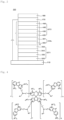
FIG. 1 to FIG. 3 illustrate an example of an organic electronic element according to the present invention.
FIG. 4 shows the formula according to one aspect of the present invention.100, 200, 300: organic electronic element 110 : the first electrode 120 : hole injection layer 130 : hole transport layer 140 : emitting layer 150 : electron transport layer 160 : electron injection layer 170 : second electrode 180 : light efficiency enhancing Layer 210 : buffer layer 220 : emitting-auxiliary layer 320 : first hole injection layer 330 : first hole transport layer 340 : first emitting layer 350 : first electron transport layer 360 : first charge generation layer 361 : second charge generation layer 420 : second hole injection layer 430 : second hole transport layer 440 : second emitting layer 450 : second electron transport layer CGL : charge generation layer ST1 : first stack ST2 : second stack - Hereinafter, some embodiments of the present invention will be described in detail. Further, in the following description of the present invention, a detailed description of known functions and configurations incorporated herein will be omitted when it may make the subject matter of the present invention rather unclear.
- In addition, terms, such as first, second, A, B, (a), (b) or the like may be used herein when describing components of the present invention. Each of these terminologies is not used to define an essence, order or sequence of a corresponding component but used merely to distinguish the corresponding component from other component(s). It should be noted that if a component is described as being "connected", "coupled", or "connected" to another component, the component may be directly connected or connected to the other component, but another component may be "connected", "coupled" or "connected" between each component.
- As used in the specification and the accompanying claims, unless otherwise stated, the following is the meaning of the term as follows.
- Unless otherwise stated, the term "halo" or "halogen" , as used herein, includes fluorine, bromine, chlorine, or iodine.
- Unless otherwise stated, the term "alkyl" or "alkyl group" , as used herein, has a single bond of 1 to 60 carbon atoms, and means saturated aliphatic functional radicals including a linear alkyl group, a branched chain alkyl group, a cycloalkyl group (alicyclic), a cycloalkyl group substituted with a alkyl or an alkyl group substituted with a cycloalkyl.
- Unless otherwise stated, the term "alkenyl" or "alkynyl" , as used herein, has double or triple bonds of 2 to 60 carbon atoms, but is not limited thereto, and includes a linear or a branched chain group.
- Unless otherwise stated, the term "cycloalkyl" , as used herein, means alkyl forming a ring having 3 to 60 carbon atoms, but is not limited thereto.
- Unless otherwise stated, the term "alkoxyl group" , "alkoxy group" or "alkyloxy group" , as used herein, means an oxygen radical attached to an alkyl group, but is not limited thereto, and has 1 to 60 carbon atoms.
- Unless otherwise stated, the term "aryloxyl group" or "aryloxy group" , as used herein, means an oxygen radical attached to an aryl group, but is not limited thereto, and has 6 to 60 carbon atoms.
- Unless otherwise stated, the term "aryl group" or "arylene group" , as used herein, has 6 to 60 carbon atoms, but is not limited thereto. Herein, the aryl group or arylene group means a monocyclic and polycyclic aromatic group, and may also be formed in conjunction with an adjacent group. Examples of "aryl group" may include a phenyl group, a biphenyl group, a fluorene group, or a spirofluorene group.
- The prefix "aryl" or "ar" means a radical substituted with an aryl group. For example, an arylalkyl may be an alkyl substituted with an aryl, and an arylalkenyl may be an alkenyl substituted with aryl, and a radical substituted with an aryl has a number of carbon atoms as defined herein.
- Also, when prefixes are named subsequently, it means that substituents are listed in the order described first. For example, an arylalkoxy means an alkoxy substituted with an aryl, an alkoxylcarbonyl means a carbonyl substituted with an alkoxyl, and an arylcarbonylalkenyl also means an alkenyl substituted with an arylcarbonyl, wherein the arylcarbonyl may be a carbonyl substituted with an aryl.
- Unless otherwise stated, the term "heterocyclic group" , as used herein, contains one or more heteroatoms, but is not limited thereto, has 2 to 60 carbon atoms, includes any one of monocyclic and polycyclic rings, and may include heteroaliphatic ring and/or heteroaromatic ring. Also, the heterocyclic group may also be formed in conjunction with an adjacent group.
- Unless otherwise stated, the term "heteroatom" , as used herein, represents at least one of N, O, S, P, or Si.
- Also, the term "heterocyclic group" may include a ring including SO2 instead of carbon consisting of cycle. For example, "heterocyclic group" includes a following compound.

- Unless otherwise stated, the term "fluorenyl group" or "fluorenylene group" , as used herein, means a monovalent or divalent functional group, in which R, R' and R" are all hydrogen in the following structures, and the term "substituted fluorenyl group" or "substituted fluorenylene group" means that at least one of the substituents R, R' , R" is a substituent other than hydrogen, and include those in which R and R' are bonded to each other to form a spiro compound together with the carbon to which they are bonded.

- The term "spiro compound" , as used herein, has a 'spiro union' , and a spiro union means a connection in which two rings share only one atom. At this time, atoms shared in the two rings are called 'spiro atoms' , and these compounds are called 'monospiro-' , 'di-spiro-' and 'tri-spiro-' , respectively, depending on the number of atoms in a compound.
- Unless otherwise stated, the term "aliphatic" , as used herein, means an aliphatic hydrocarbon having 1 to 60 carbon atoms, and the term "aliphatic ring" , as used herein, means an aliphatic hydrocarbon ring having 3 to 60 carbon atoms.
- Unless otherwise stated, the term "ring" , as used herein, means an aliphatic ring having 3 to 60 carbon atoms, or an aromatic ring having 6 to 60 carbon atoms, or a hetero ring having 2 to 60 carbon atoms, or a fused ring formed by the combination of them, and includes a saturated or unsaturated ring.
- Other hetero compounds or hetero radicals other than the above-mentioned hetero compounds include, but are not limited thereto, one or more heteroatoms.
- Unless otherwise stated, the term "substituted or unsubstituted" , as used herein, means that substitution is substituted by at least one substituent selected from the group consisting of, but is not limited thereto, deuterium, halogen, an amino group, a nitrile group, a nitro group, a C1-C20 alkyl group, a C1-C20 alkoxyl group, a C1-C20 alkylamine group, a C1-C20 alkylthiophene group, a C6-C20 aryl thiophene group, a C2-C20 alkenyl group, a C2-C20 alkynyl group, a C3-C20 cycloalkyl group, a C6-C20 aryl group, a C6-C20 aryl group substituted by deuterium, a C8-C20 arylalkenyl group, a silane group, a boron group, a germanium group, and a C2-C20 heterocyclic group.
- Unless otherwise expressly stated, the Formula used in the present invention, as used herein, is applied in the same manner as the substituent definition according to the definition of the exponent of the following Formula.


- Hereinafter, a compound according to an aspect of the present invention and an organic electronic element comprising the same will be described.
- According to a specific example of the present invention, there is provided a compound represented by Formula (6-1).

- In Formula (6-1), each symbol may be defined as follows.
- 1) X1, and X3 are each independently O or S,
- 2) Y1 is O or S,
- 3) e, f, g, h, j, r, s and t are each independently an integer of 0 to 4, q is an integer of 0 to 3,
wherein in case e, f, g, h, j, q and r are 2 or more, R1, R2, R3, R4, and R6 are each in plural being the same or different, and an adjacent plurality of R1 or a plurality of R2 or a plurality of R3 or a plurality of R4 or a plurality of R6 or a plurality of R9 or a plurality of R10 or a plurality of R11 or a plurality of R12 may be bonded to each other to form a ring, - 4) n is an integer of 0 to 3,
- 5) L3, L4, and L9 are the same or different from each other, and are each independently selected from the group consisting of single bond; a C6-C60 arylene group; a fluorenylene group; a fused ring group of a C3-C60 aliphatic ring and a C6-C60 aromatic ring; a C2-C60 heterocyclic group;
- 6) Ar3 is selected from the group consisting of hydrogen; deuterium; tritium; halogen; cyano group; nitro group; C6-C60 aryl group; a fluorenyl group; a C2-C60 heterocyclic group including at least one heteroatom of O, N, S, Si or P; a fused ring group of a C3-C60 aliphatic ring and a C6-C60 aromatic ring; C1-C50 alkyl group; C2-C20 alkenyl group; C2-C20 alkynyl group; C1-C30 alkoxyl group; C6-C30 aryloxy group; and -L'-N(Ra)(Rb);
- 7) R1, R2, R3, R4, R6, R9, R10, R11and R12 are the same or different from each other, and are each independently selected from the group consisting of hydrogen; deuterium; tritium; halogen; cyano group; nitro group; C6-C60 aryl group; a fluorenyl group; a C2-C60 heterocyclic group including at least one heteroatom of O, N, S, Si or P; a fused ring group of a C3-C60 aliphatic ring and a C6-C60 aromatic ring; C1-C50 alkyl group; C2-C20 alkenyl group; C2-C20 alkynyl group; C1-C30 alkoxyl group; C6-C30 aryloxy group; and -L'-N(Ra)(Rb):
- 8) wherein L' is selected from the group consisting of a single bond; a C6-C60 arylene group; a fluorenylene group; C3-C60 aliphatic ring; a C2-C60 heterocyclic group including at least one heteroatom of O, N, S, Si or P; a combination thereof; wherein Ra and Rb are each independently selected from the group consisting of a C6-C60 aryl group; a fluorenyl group; C3-C60 aliphatic ring; a C2-C60 heterocyclic group including at least one heteroatom of O, N, S, Si or P;
- 9) wherein, the aryl group, arylene group, heterocyclic group, fluorenyl group, fluorenylene group, fused ring group, alkyl group, alkenyl group, alkoxy group and aryloxy group may be substituted with one or more substituents selected from the group consisting of deuterium; halogen; silane group; siloxane group; boron group; germanium group; cyano group; nitro group; C1-C20 alkylthio group; C1-C20 alkoxyl group; C1-C20 alkyl group; C2-C20 alkenyl group; C2-C20 alkynyl group; C6-C25 aryl group; C6-C25 aryl group substituted with deuterium; a fluorenyl group; C2-C20 heterocyclic group; C3-C20 cycloalkyl group; C7-C20 arylalkyl group; C8-C20 arylalkenyl group; and -L'-N(Ra)(Rb); wherein the substituents may be bonded to each other to form a saturated or unsaturated ring, wherein the term 'ring' means a C3-C60 aliphatic ring, a C6-C60 aromatic ring, a C2-C60 heterocyclic group, a fused ring formed by combination thereof.
- Formula 6-1 includes a compound represented by Formula 6-2.


- 1) X1, X3, Y1,R1, R2, R3, R4, R6, R9, R10, R11, R12, L3, L4, Ar3, e, f, g, h, j, n, q, r, s, and t are the same as defined in Formula 6-1.
- Specifically, the compound represented by Formula 6-1 may be a compound represented by any one of the following compounds P2-1 to P2-55, but is not limited thereto.


- Referring to
FIG. 1 , the organic electronic element(100) according to the present invention includes a first electrode(110), a second electrode(170), an organic material layer comprising single compound represented by Formula 1 or 2 or more compounds between the first electrode(110) and the second electrode(170), Here, the first electrode(110) may be an anode or a positive electrode, and the second electrode(170) may be a cathode or a negative electrode. In the case of an inverted organic electronic element, the first electrode may be a cathode, and the second electrode may be an anode. - The organic material layer may sequentially include a hole injection layer(120), a hole transport layer (130), an emitting layer(140), an electron transport layer(150), and an electron injection layer(160) formed in sequence on the first electrode(110). Here, the remaining layers except the emitting layer(140) may not be formed. The organic material layer may further include a hole blocking layer, an electron blocking layer, an emitting-auxiliary layer(220), a buffer layer(210), etc., and the electron transport layer(150) and the like may serve as a hole blocking layer.(see
FIG. 2 ) - Also, the organic electronic element according to an embodiment of the present invention may further include a protective layer or a light efficiency enhancing layer(180). The light efficiency enhancing layer may be formed on a surface not in contact with the organic material layer among both surfaces of the first electrode or on a surface not in contact with the organic material layer among both surfaces of the second electrode. The compound according to an embodiment of the present invention applied to the organic material layer may be used as a material for a hole injection layer(120), a hole transport layer (130), an emitting-auxiliary layer(220), an electron transport auxiliary layer, an electron transport layer(150), an electron injection layer(160), a host or dopant of an emitting layer(140) or the light efficiency enhancing layer. Preferably, for example, the compound according to Formula 1 of the present invention may be used as a material for the emitting-auxiliary layer.
- The organic material layer may include 2 or more stacks including a hole transport layer, an emitting layer, and an electron transport layer sequentially formed on the anode, and may further include a charge generation layer formed between the 2 or more stacks (see
FIG. 3 ). - Otherwise, even if the same core is used, the band gap, the electrical characteristics, the interface characteristics, and the like may vary depending on which substituent is bonded at which position, therefore the choice of core and the combination of sub-substituents associated therewith is also very important, and in particular, when the optimal combination of energy levels and T1 values and unique properties of materials(mobility, interfacial characteristics, etc.) of each organic material layer is achieved, a long life span and high efficiency can be achieved at the same time.
- The organic electroluminescent device according to an embodiment of the present invention may be manufactured using a PVD (physical vapor deposition) method. For example, a metal or a metal oxide having conductivity or an alloy thereof is deposited on a substrate to form a cathode, and the organic material layer including the hole injection layer(120), the hole transport layer(130), the emitting layer(140), the electron transport layer(150), and the electron injection layer(160) is formed thereon, and then depositing a material usable as a cathode thereon can manufacture an organic electroluminescent device according to an embodiment of the present invention.
- Also, the present invention provides the organic electronic element wherein the organic material layer is formed by one of a spin coating process, a nozzle printing process, an inkjet printing process, a slot coating process, a dip coating process or a roll-to-roll process, and the organic material layer provides an organic electronic element comprising the compound as an electron transport material.
- As another specific example, the present invention provides an organic electronic element that is used by mixing the same or different compounds of the compound represented by Formula 6-1 to the organic material layer.
- In another aspect, the present invention provides an emitting-auxiliary layer composition comprising a compound represented by Formula 6-1, and provides an organic electronic element comprising the emitting-auxiliary layer.
- The present invention also provides an electronic device comprising a display device including the organic electronic element; and a control unit for driving the display device.
- According to another aspect, the present invention provides an display device wherein the organic electronic element is at least one of an OLED, an organic solar cell, an organic photo conductor, an organic transistor(organic TFT) and an element for monochromic or white illumination. Here, the electronic device may be a wired/wireless communication terminal which is currently used or will be used in the future, and covers all kinds of electronic devices including a mobile communication terminal such as a cellular phone, a personal digital assistant(PDA), an electronic dictionary, a point-to-multipoint(PMP), a remote controller, a navigation unit, a game player, various kinds of TVs, and various kinds of computers.
- Hereinafter, Synthesis Examples of the compound represented by Formula 6-1 of the present invention and preparation examples of the organic electronic element of the present invention will be described in detail by way of example, but are not limited to the following examples.
- The compound (Final product) represented by Formula 6-1 according to the present invention may be prepared by reacting as in Scheme 1, but is not limited thereto.
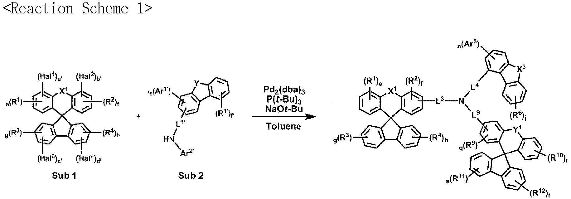
- 1) X1, X3, Y1, R1, R2, R3, R4, R6, R9, R10, R11, R12, L3, L4, Ar3, , f, g, h, j, n, q, r, s, and t are the same as defined above,
- 2) Hal1 to Hal4 are each independently Br or Cl,
- 3) a' to d' are each independently 0 or 1, at least one of a' to d' is 1,
- 4) Y is the same as the definition of X3,
- 5) Ar1' is the same as the definition of Ar3,
- 6) Ar2' is the same as the definition of Ar4,
- 7) R1' is the same as the definition of R6,
- 8) L1' is the same as the definition of L4,
- 9) e' is an integer of 0 to 3, f' is an integer of 0 to 4.
- Sub 1 of Reaction Scheme 1 may be synthesized by the reaction path of Scheme 2, but is not limited thereto. When X1 is -OH, the synthesis path of (1) of Reaction Scheme 2 is followed, and when X1 is -SH, the synthesis path of (2) of Reaction Scheme 2 is followed.

- In Reaction Scheme 2,
X1, R1, R2, R3, R4, e, f, g, h, Hal1, Hal2, Hal3, Hal4, and a', b', c', d' are the same as defined in Formula 1. - Synthesis examples of specific compounds belonging to Sub 1 are as follows.
-


- 5-chloro-2-iodobenzoic acid (50.0 g, 177 mmol), Phenol (33.3 g, 354 mmol), 1,8-diazabicyclo[5.4.0]undec-7-ene (DBU) (80.9 g, 531 mmol), pyridine (2.9 mL), Copper powder (1.5 g, 23 mmol), CuI (1.5 g, 7.97 mmol) were placed in a round bottom flask, and DMF (1.2 L) was added, followed by refluxing for 3 hours. When the reaction is complete, cool to room temperature and add 3M HCl until precipitation is complete. Thereafter, the precipitate was washed with water and dried to obtain 38.3 g (yield 87%) of the product.
- Sub 1-1-a (38.3 g, 154 mmol) obtained in the above synthesis was added to a round bottom flask, and H2SO4 (1.1mL, 21.5 mmol) was added, followed by refluxing until all the starting materials were dissolved. When all the starting materials are dissolved, cool to room temperature and add ice water to precipitate. Thereafter, the precipitate was washed with water, dried, dissolved in CH2Cl2, and recrystallized with a Silicagel column to obtain 23.09 g (yield 65%) of the product.
- 2-bromo-1,1'-biphenyl (23.3 g, 99.7 mmol) was dissolved in THF (270 mL) in a round bottom flask under a nitrogen atmosphere, and then cooled to -78° C.
- Then, n-BuLi (40 mL) was slowly titrated and the mixture was stirred for 30 minutes. Subsequently, Sub1-1-b (23 g, 99.7 mmol) obtained in the above synthesis was dissolved in THF (140 mL), and then slowly titrated into a reaction round bottom flask. After stirring for an additional 1 hour at - 78 °C, it is gradually raised to room temperature. When the reaction was completed, the product was extracted with Ethyl acetate and water, and the organic layer was dried over MgSO4 and concentrated, and the resulting compound was recrystallized in a silicagel column to obtain 32.6 g (yield 85%) of the product.
- Sub 1-1-c (32 g, 84.7 mmol) obtained in the above synthesis, acetic acid (208 mL), and concentrated hydrochloric acid (34.6 mL) were added to a round bottom flask, followed by stirring at 60 to 80° C for 3 hours under a nitrogen atmosphere. When the reaction was completed, the product was extracted with CH2Cl2 and water, and the organic layer was dried over MgSO4 and concentrated, and the resulting compound was recrystallized with a silicagel column to obtain 27.7 g (91% yield) of the product.
-


- 2-iodobenzoic acid (50.0 g, 202 mmol), Thiophenol (22.2 g, 202 mmol), Potassium hydroxide (56.6 g, 1008 mmol), Copper powder (1.3 g, 20.2 mmol) were placed in a round bottom flask and water (1.3 L) was added, followed by refluxing for 12 hours. When the reaction is complete, cool to room temperature and add 3M HCl until precipitation is complete. Thereafter, the precipitate was washed with water and dried to obtain 41.3 g (yield 89%) of the product.
- Sub 1-11-a (41.3 g, 179 mmol) and H2SO4 (1.3 mL) obtained in the above synthesis was used for the synthesis of Sub 1-1-b to obtain 25.9 g (68% yield) of a product.
- 2-bromo-4'-chloro-1,1'-biphenyl (32.6 g, 122 mmol), n-BuLi (49 mL), Sub 1-11-b (25.9 g, 122 mmol) obtained in the above synthesis was used for the synthesis of Sub 1-1-c to obtain 40.1 g (82% yield) of a product.
- Sub 1-11-c (40.1 g, 100 mmol) obtained in the above synthesis, acetic acid (250 mL), and concentrated hydrochloric acid (40 mL) were obtained by using the synthesis method of Sub 1-1 above to obtain 31.8 g (yield 83%) of the product.
-


- 3-chloro-2-iodobenzoic acid (30.0 g, 106.2 mmol), Thiophenol (11.7 g, 106.2 mmol), Potassium hydroxide (29.8 g, 531 mmol), Copper powder (0.67 g, 10.6 mmol) were used to obtain 23.6 g of a product (84% yield) using the synthesis method of Sub 1-11-a.
- Sub 1-20-a (23.6 g, 89.2 mmol) and H2SO4 (0.67 mL) obtained in the above synthesis was used for the synthesis of Sub 1-1-b to obtain 14.5 g (66% yield) of a product.
- 1-(2-bromophenyl)naphthalene (16.6 g, 58.8 mmol), n-BuLi (24 mL), Sub1-20-b (14.5 g, 58.8 mmol) obtained in the above synthesis was used for the synthesis of Sub 1-1-c to obtain 21.5 g (81% yield) of a product.
- Sub 1-20-c (21 g, 46.6 mmol) obtained in the above synthesis, acetic acid (116 mL), and concentrated hydrochloric acid (19 mL) were obtained by using the synthesis method of Sub 1-1 above to obtain 15.9 g (yield 79%) of the product.
-


- 2-iodobenzoic acid (15 g, 60.5 mmol), Sub1'-55 (37.9 g, 120.1 mmol), 1,8-diazabicyclo[5.4.0]undec-7-ene (DBU) (27.6 g, 181.4 mmol), pyridine (0.98 mL), Copper powder (0.5 g, 7.9 mmol), CuI (0.5 g, 2.7 mmol) were used to obtain 27.7 g of a product (78% yield) using the synthesis method of Sub 1-1-a.
- Sub 1-55-a (27.7 g, 47.1 mmol) and H2SO4 (0.35 mL) obtained in the above synthesis was used for the synthesis of Sub 1-1-b to obtain 17.7 g (64% yield) of a product.
- 2-bromo-2'-chloro-1,1'-biphenyl (7.8 g, 29 mmol), n-BuLi (11.7 mL), Sub 1-55-b (17 g, 29 mmol) obtained in the above synthesis was used for the synthesis of Sub 1-1-c to obtain 17.3 g (77% yield) of a product.
- Sub 1-55-c (17.3 g, 22.3 mmol) obtained in the above synthesis, acetic acid (56 mL), and concentrated hydrochloric acid (9.3 mL) were obtained by using the synthesis method of Sub 1-1 above to obtain 13.5 g (yield 80%) of the product.
-


- 3-chloro-2-iodobenzoic acid (18 g, 63.7 mmol), Sub1'-140 (28.3 g, 63.7 mmol), Potassium hydroxide (17.9 g, 318.6 mmol), Copper powder (0.4 g, 6.4 mmol) were used to obtain 30.1 g of a product (79% yield) using the synthesis method of Sub 1-11-a.
- Sub 1-140-a (30.1 g, 46.3 mmol) and H2SO4 (0.35 mL) obtained in the above synthesis was used for the synthesis of Sub 1-1-b to obtain 18.1 g (62% yield) of a product.
- Subl"-140 (19.9 g, 30.3 mmol), n-BuLi (12.2 mL), Sub1-141-b (18.1 g, 30.3 mmol) obtained in the above synthesis were used for the synthesis of Sub 1-1-c to obtain 24.5 g (70% yield) of a product.
- Sub 1-140-c (24.5 g, 21.1 mmol) obtained in the above synthesis, acetic acid (53 mL), and concentrated hydrochloric acid (8.8 mL) were obtained by using the synthesis method of Sub 1-1 above to obtain 18.1 g (yield 75%) of the product.
-


- 4-chloro-2-iodobenzoic acid (12 g, 42.5 mmol), 3-chlorophenol (10.9 g, 84.97 mmol), 1,8-diazabicyclo[5.4.0]undec-7-ene (DBU) (19.4 g, 127.5 mmol), pyridine (0.69 mL), Copper powder (0.35 g, 5.5 mmol), CuI (0.36 g, 1.9 mmol) were used to obtain 9.7 g of a product (81% yield) using the synthesis method of Sub 1-1-a.
- Sub 1-152-a (9.7 g, 34.3 mmol) and H2SO4 (0.26 mL) obtained in the above synthesis was used for the synthesis of Sub 1-1-b to obtain 6.6 g (73% yield) of a product.
- The obtained Sub 1-152-b (6.6 g, 24.9 mmol), Sub 2-20 (17.5 g, 49.8 mmol), Pd2(dba)3 (0.68 g, 0.75 mmol), P(t-Bu)3 (50wt% Sol.) (0.6 mL, 1.5 mmol), t-BuONa (7.18 g, 74.7 mmol) were added to anhydrous Toluene (150 mL) and reacted for 3 hours. After confirming the completion of the reaction, extraction was performed with CH2Cl2 and water, and the organic layer was dried over MgSO4 and concentrated. The resulting compound was silicagel column and recrystallized to give a product 14.8 g (yield 60%).
- Sub 1"-152 (8.97 g, 14.9 mmol), n-BuLi (6 mL), Sub 1-152-b' (14.8 g, 14.9 mmol) obtained in the above synthesis was used to obtain a product 14.0 g (62% yield) using the synthesis method of Sub 1-1-c.
- Sub 1-152-c (14 g, 9.3 mmol) obtained in the above synthesis, acetic acid (23 mL), and concentrated hydrochloric acid (3.8 mL) were used to obtain 8.7 g (63% yield) of the product using the synthesis method of Sub 1-1.
- Meanwhile, the compound belonging to Sub 1 may be the following compound, but is not limited thereto, and Table 1 shows FD-MS (Field Desorption-Mass Spectrometry) values of the compound belonging to Sub 1.


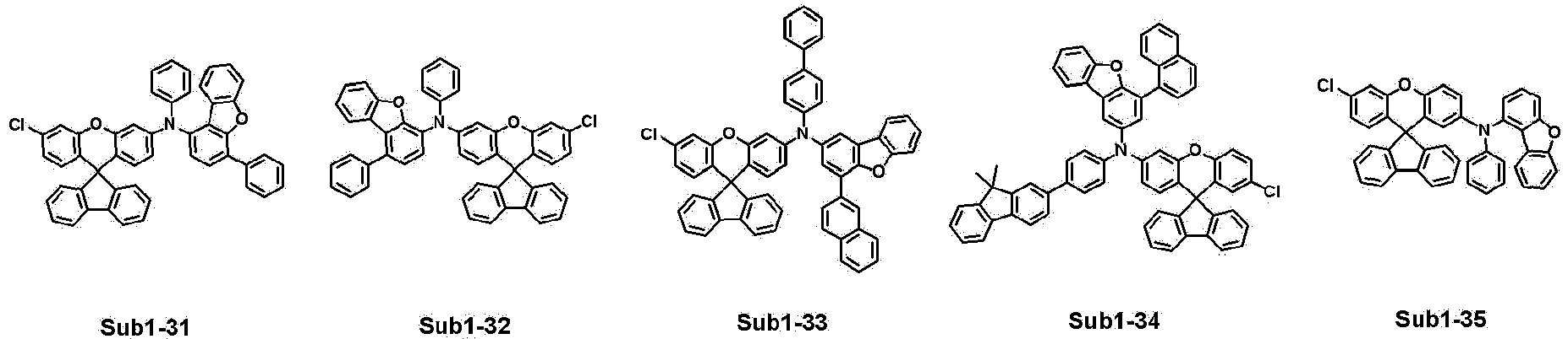


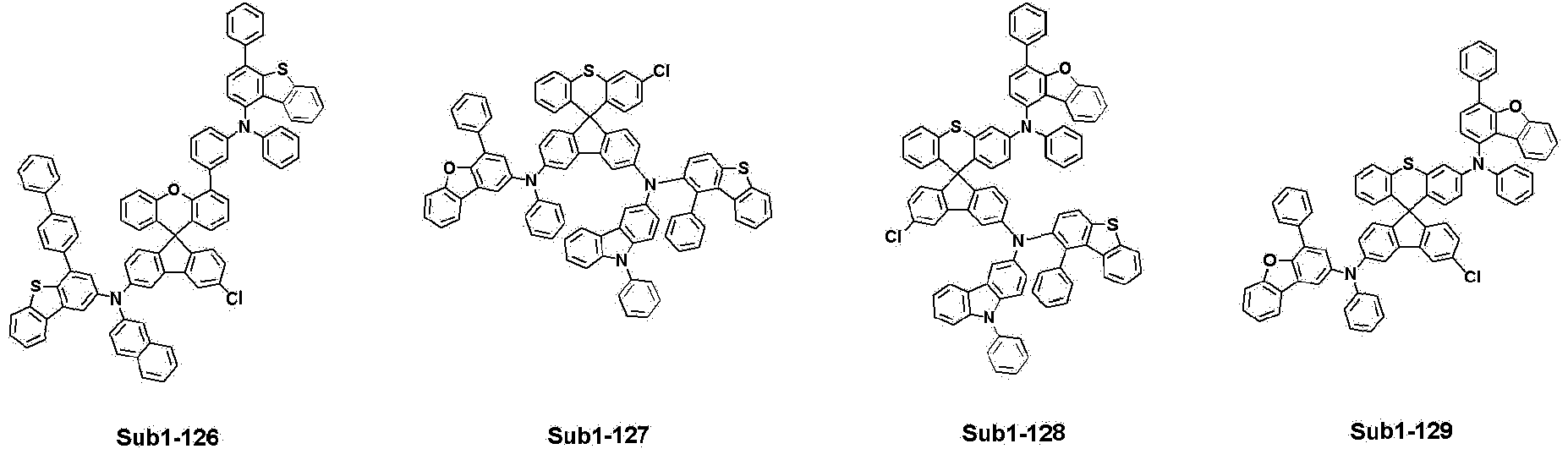


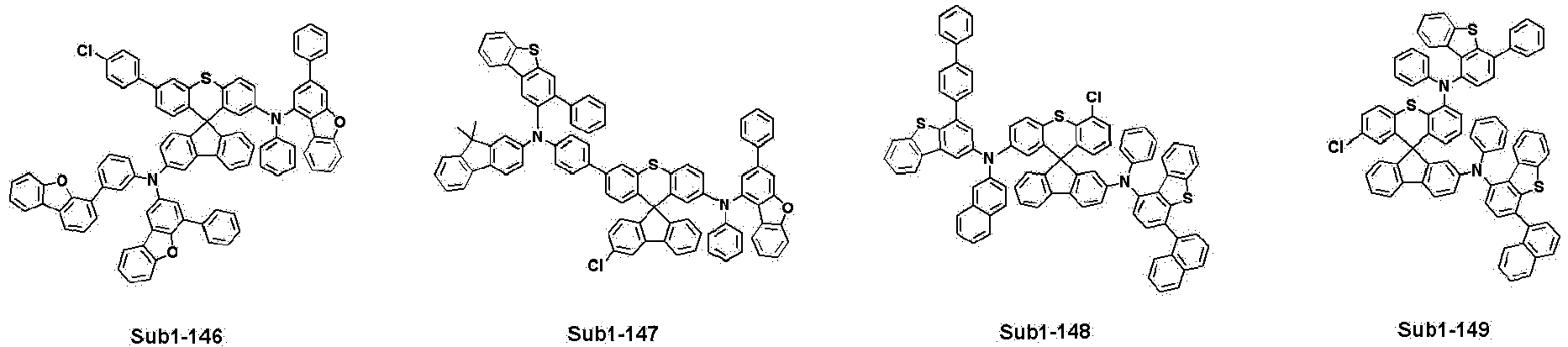


Table 1 compound FD-MS compound FD-MS Subl-1 m/z=366.08(C25H15ClO=366.84) Subl-2 m/z=366.08(C25H15ClO=366.84) Subl-3 m/z=366.08(C25H15ClO=366.84) Subl-4 m/z=366.08(C25H15ClO=366.84) Subl-5 m/z=366.08(C25H15ClO=366.84) Subl-6 m/z=366.08(C25H15ClO=366.84) Subl-7 m/z=366.08(C25H15ClO=366.84) Subl-8 m/z=366.08(C25H15ClO=366.84) Subl-9 m/z=382.06(C25H15ClS=382.91) Subl-10 m/z=382.06(C25H15ClS=382.91) Subl-11 m/z=382.06(C25H15ClS=382.91) Subl-12 m/z=382.06(C25H15ClS=382.91) Subl-13 m/z=382.06(C25H15ClS=382.91) Subl-14 m/z=382.06(C25H15ClS=382.91) Subl-15 m/z=382.06(C25H15ClS=382.91) Subl-16 m/z=382.06(C25H15ClS=382.91) Subl-17 m/z=432.07(C29H17ClS=432.97) Subl-18 m/z=432.07(C29H17ClS=432.97) Subl-19 m/z=432.07(C29H17ClS=432.97) Subl-20 m/z=432.07(C29H17ClS=432.97) Subl-21 m/z=442.11(C31H19ClO=442.94) Subl-22 m/z=408.07(C27H17ClS=408.94) Subl-23 m/z=442.11(C31H19ClO=442.94) Subl-24 m/z=508.11(C35H21ClS=509.06) Subl-25 m/z=574.15(C40H27ClS=575.17) Subl-26 m/z=442.11(C31H19ClO=442.94) Subl-27 m/z=442.11(C31H19ClO=442.94) Subl-28 m/z=532.12(C37H21ClO2=533.02) Subl-29 m/z=443.11(C30OH18ClNO=443.93) Subl-30 m/z=416.10(C23H17ClO=416.90) Subl-31 m/z=699.20(C49H30ClNO2=700.23) Subl-32 m/z=699.20(C49H30ClNO2=700.23) Subl-33 m/z=825.24(C59H36ClNO2=826.39) Subl-34 m/z=941.31(C68H44ClNO2=942.56) Subl-35 m/z=623.17(C43H26ClNO2=624.14) Subl-36 m/z=825.24(C59H36ClNO2=826.39) Subl-37 m/z=699.20(C49H30ClNO2=700.23) Subl-38 m/z=715.17(C49H30ClNOS=716.3) Subl-39 m/z=805.18(C55H32ClNO2S=806.38) Subl-40 m/z=749.21(C53H32ClNO2=750.29) Subl-41 m/z=892.29(C63H41ClN2O2=893.48) Subl-42 m/z=623.17(C43H26ClNO2=624.14) Subl-43 m/z=841.27(C60H40ClNO2=842.44) Subl-44 m/z=805.18(C55H32ClNO2S=806.38) Subl-45 m/z=775.23(C55H34ClNO2=776.33) Subl-46 m/z=815.26(C58H38ClNO2=816.40) Subl-47 m/z=623.17(C43H26ClNO2=624.14) Subl-48 m/z=699.20(C49H30ClNO2=700.23) Subl-49 m/z=936.22(C63H37ClN2O3S=937.51) Subl-50 m/z=855.20(C59H34ClNO2S=856.44) Subl-51 m/z=699.20(C49H30ClNO2=700.23) Subl-52 m/z=699.20(C49H30ClNO2=700.23) Subl-53 m/z=897.25(C62H40ClNO2S=898.52) Subl-54 m/z=957.28(C68H44ClNOS=958.62) Subl-55 m/z=739.19(C51B30ClNO3=740.26) Subl-56 m/z=917.25(C65H40ClNOS=918.55) Subl-57 m/z=791.20(C55H34ClNOS=792.39) Subl-58 m/z=699.20(C49H30ClNO2=700.23) Subl-59 m/z=897.19(C61H36ClNOS2=898.54) Subl-60 m/z=749.21(C53H32ClNO2=750.29) Subl-61 m/z=805.18(C55B32ClNO2S=806.38) Subl-62 m/z=755.17(C51B30ClNO2S=756.32) Subl-63 m/z=1088.32(C76H49ClN2O2S=1089.75) Subl-64 m/z=699.20(C49H30ClNO2=700.23) Subl-65 m/z=891.29(C64B42ClNO2=892.50) Subl-66 m/z=639.14(C43H26ClNOS=640.20) Subl-67 m/z=715.17(C49B30ClNOS=716.30) Subl-68 m/z=715.17(C49H30ClNOS=716.3) Subl-69 m/z=841.22(C59H36ClNOS=842.45) Subl-70 m/z=957.28(C68H44ClNOS=958.62) Subl-71 m/z=639.14(C43H26ClNOS=640.20) Subl-72 m/z=917.25(C65H40ClNOS=918.55) Subl-73 m/z=841.22(C59H36ClNOS=842.45) Subl-74 m/z=731.15(C49B30ClNS2=732.36) Subl-75 m/z=821.16(C55H32ClNOS2=822.44) Subl-76 m/z=765.19(C53H32ClNOS=766.36) Subl-77 m/z=908.26(C63H41ClN2OS=909.54) Subl-78 m/z=873.23(C60B40ClNS2=874.56) Subl-79 m/z=731.15(C49B30ClNS2=732.36) Subl-80 m/z=821.16(C55H32ClNOS2=822.44) Subl-81 m/z=715.17(C49H30ClNOS=716.30) Subl-82 m/z=791.20(C55H34ClNOS=792.39) Subl-83 m/z=639.14(C43H26ClNOS=640.20) Subl-84 m/z=847.21(C58H38ClNS2=848.52) Subl-85 m/z=936.22(C63H37ClN2O3S=937.51) Subl-86 m/z=731.15(C49B30ClNS2=732.36) Subl-87 m/z=731.15(C49B30ClNS2=732.36) Subl-88 m/z=855.20(C59H34ClNO2S=856.44) Subl-89 m/z=715.17(C49H30)ClNOS=716.30) Subl-90 m/z=947.26(C66B42ClNO2S=948.58) Subl-91 m/z=755.17(C51B30ClNO2S=756.32) Subl-92 m/z=1007.30(C72H46ClNOS=1008.68) Subl-93 m/z=791.20(C55H34ClNOS=792.39) Subl-94 m/z=917.25(C65H40ClNOS=918.55) Subl-95 m/z=956.26(C67H41ClN2OS=957.59) Subl-96 m/z=972.24(C67H41ClN2S2=973.65) Subl-97 m/z=765.19(C53H32ClNOS=766.36) Subl-98 m/z=821.16(C55H32ClNOS2=822.44) Subl-99 m/z=771.15(C51H30ClNOS2=772.38) Subl-100 m/z=1104.30(C76H49ClN2OS2=1105.81) Subl-101 m/z=907.27(C64H42ClNOS=908.56) Subl-102 m/z=715.17(C49H30ClNOS=716.03) Subl-103 m/z=1032.31(C73H45ClN2O3=1033.62) Subl-104 m/z=1048.29(C73B45ClN2O2S=1049.69) Subl-105 m/z=1048.29(C73B45ClN2O2S=1049.69) Subl-106 m/z=1154.28(C79H47ClN2O2S2=1155.83) Subl-107 m/z=1264.35(C89H53ClN2O3S=1265.92) Subl-108 m/z=1174.34(C83B51ClN2O2S=1175.84) Subl-109 m/z=1406.42(C100H63ClN2O3S=1408.13) Subl-110 m/z=1274.39(C91H55ClN2O4=1275.90) Subl-111 m/z=1240.38(C88B57ClN2O2S=1241.95) Subl-112 m/z=1048.29(C73B45ClN2O2S=1049.69) Subl-113 m/z=1174.34(C83H51ClN2O2S=1175.84) Subl-114 m/z=1190.31(C83H51ClN2OS2=1191.90) Subl-115 m/z=1138.30(C79H47ClN2O3S=1139.77) Subl-116 m/z=1154.28(C79H47ClN2O2S2=1155.83) Subl-117 m/z=1048.29(C73B45ClN2O2S=1049.69) Subl-118 m/z=1270.34(C88H55ClN2O2S2=1271.99) Subl-119 m/z=1188.32(C83B49ClN2O3S=1189.83) Subl-120 m/z=1214.37(C86H55ClN2O2S=1215.91) Subl-121 m/z=1141.29(C78H48ClN3OS2=1142.83) Subl-122 m/z=1140.3O(C79B49ClN2OS2=1141.84) Subl-123 m/z=1141.29(C78B48ClN3OS2=1142.83) Subl-124 m/z=1250.37(C89H55ClN2O2S=1251.94) Subl-125 m/z=1124.32(C79H49ClN2O2S=1125.78) Subl-126 m/z=1266.34(C89H55ClN2OS2=1268.00) Subl-127 m/z=1229.32(C85H52ClN3OS2=1230.94) Subl-128 m/z=1229.32(C85H52ClN3OS3=1230.94) Subl-129 m/z=1048.29(C73H45ClN2O2S=1049.69) Subl-130 m/z=1114.28(C77H47ClN2OS2=1115.81) Subl-131 m/z=1170.25(C79H47ClN2OS3=1171.89) Subl-132 m/z=1204.29(C83H49ClN2O2S2=1205.89) Subl-133 m/z=1477.44(C103H68ClN3O2S2=1479.27) Subl-134 m/z=1154.28(C79H47ClN2O2S2=1155.83) Subl-135 m/z=1471.49(C105H70ClN3O2S=1473.24) Subl-136 m/z=1064.27(C73H45ClN2OS2=1065.75) Subl-137 m/z=1256.36(C88H57ClN2OS2=1258.01) Subl-138 m/z=1240.38(C88H57ClN2O2S=1241.95) Subl-139 m/z=1140.30(C79H49ClN2OS2=1141.84) Subl-140 m/z=1140.30(C79H49ClN2OS2=1141.84) Subl-141 m/z=1124.32(C79H49ClN2O2S=1125.78) Subl-142 m/z=1170.25(C79H47ClN2OS3=1171.89) Subl-143 m/z=1280.32(C89H53ClN2O2S2=1281.99) Subl-144 m/z=1190.31(C83H51ClN2OS2=1191.90) Subl-145 m/z=1422.40(C100H63ClN2O2S2=1424.19) Subl-146 m/z=1290.36(C91H55ClN2O3S=1291.96) Subl-147 m/z=1256.36(C88H57ClN2OS2=1258.01) Subl-148 m/z=1256.31(C87H53ClN2S3=1258.03) Subl-149 m/z=1130.26(C77H47ClN2S3=1131.87) Subl-150 m/z=1206.29(C83H51ClN2S3=1207.97) Subl-151 m/z=1236.39(C83H62Cl2N2O3S=1238.38) Subl-152 m/z=1493.57(C103H84ClN3O2S2=1495.39) Subl-153 m/z=1599.56(C109B86ClN3O2S3=1601.54) Subl-154 m/z=1214.24(C81H48Cl2N2S3=1216.37) Subl-155 m/z=1082.25(C73H44Cl2N2O2S=1084.13) Subl-156 m/z=508.11(C35H21ClS=509.06) Subl-157 m/z=442.11(C31H19ClO=442.94) Subl-158 m/z=1252.36(C83H62Cl2N2O2S2=1254.44) Subl-159 m/z=1509.55(C103H84ClN3OS3=1511.46) Subl-160 m/z=1615.53(C109B86ClN3OS4=1617.60) Subl-161 m/z=391.08(C26H14ClNO=391.85) Subl-162 m/z=459.08(C30H18ClNS=459.99) Subl-163 m/z=442.11(C31H19ClO=442.94) Subl-164 m/z=442.11(C31H19ClO=442.94) Subl-165 m/z=442.11(C31H19ClO=442.94) Subl-166 m/z=458.09(C31H19ClS=459.00) Subl-167 m/z=458.09(C31B19ClS=459.00) Subl-168 m/z=458.09(C31H19ClS=459.00) Subl-169 m/z=391.08(C26H14ClNO=391.85) Subl-170 m/z=408.07(C27H17ClS=408.94) Subl-171 m/z=416.10(C29H17ClO=416.90) Subl-172 m/z=460.08(C29H17ClN2S=460.98) - Sub 2 of Reaction Scheme 1 may be synthesized by the reaction route of Scheme 3, but is not limited thereto. Sub 3 and Sub 4 are also included in Sub 2.
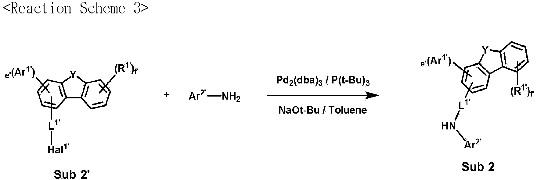
- In Reaction Scheme 3,
Y, Ar1', Ar2', R1', L1', e' and f' are the same as defined above, Hal1' is Br or Cl. - Synthesis examples of specific compounds belonging to Sub 2 are as follows.
-


- 4-bromo-2-chlorophenol (15 g, 73.5 mmol) was dissolved in a round bottom flask with DMF (400 mL) and iodobenzene (16.8 g, 80.9 mmol), K2CO3 (20.3 g 147.1 mmol), Cu (2.3 g, 36.8 mmol), Dibenzo-18-crown-6 (1.6 g, 4.4 mmol) were added and stirred at 120° C. When the reaction was completed, the solvent was removed, extracted with CH2Cl2 and water, the organic layer was dried over MgSO4, concentrated, and the resulting compound was silicagel column to obtain 16.5 g (yield 79%) of the product.
- Acetic acid (400 mL) was added to 4-bromo-2-chloro-1-phenoxybenzene (16 g, 56.4 mmol)Pd(OAc)2 (0.63 g, 2.8 mol), K2CO3 (7.8 g, 56.4 mol) and stirred at 120° C for 48 hours. When the reaction was completed, the solvent was removed, extracted with Ethyl Acetate and water, the organic layer was dried over MgSO4, concentrated, and the resulting compound was silicagel column to obtain 6.7 g (yield 42%) of the product.

- Sub 2-8-b (6.7 g, 23.8 mmol) obtained in the above synthesis, phenylboronic acid (2.9 g, 23.8 mmol) was added, dissolved in THF (100 mL), and Pd(PPh3)4 (1.4 g, 1.2 mmol) and K2CO3 (19.9 g, 71.4 mmol) were added, respectively, and then refluxed for 24 hours. When the reaction was completed, the solvent was removed, extracted with CH2Cl2 and water, the organic layer was dried over MgSO4, concentrated, and the resulting compound was silicagel column to obtain 4.98 g (yield 75%) of the product.
- After dissolving Sub 2-8-c (4.98 g, 17.9 mmol) obtained in the above synthesis with Toluene (100 ml) in a round bottom flask, Aniline (1.83 g, 19.7 mmol), Pd2(dba)3 (0.49 g, 0.54 mmol), P(t-Bu)3 (50wt% Sol.) (0.43 mL, 1.07 mmol), NaOt-Bu (5.2 g, 53.6 mmol) were added and stirred at 80° C. When the reaction was completed, the solvent was removed, extracted with CH2Cl2 and water, the organic layer was dried over MgSO4, concentrated, and the resulting compound was silicagel column to obtain 4.8 g (yield 80%) of the product.
-


- (2-(Methylthio)phenyl)boronic acid (30 g, 137.6 mmol) was dissolved in a round bottom flask with THF (300 mL) and 4-bromo-2-chloroiodobenzene (43.7g, 137.6 mmol), Pd(PPh3)4 (4.8 g, 4.1 mmol), K2CO3 (57 g, 412.7 mmol), and water (100 mL) were added and stirred at 80° C. When the reaction was completed, the solvent was removed, extracted with CH2Cl2 and water, the organic layer was dried over MgSO4, concentrated, and the resulting compound was silicagel column to obtain 37.5 g (yield 75%) of the product.
- Sub 2-43-a (37 g, 101.7 mmol) obtained in the above synthesis was dissolved in AcOH (300 mL) in a round bottom flask, H2O2 (8.7 mL, 101.7 mmol) was added and stirred at room temperature. When the reaction was completed, the solvent was removed, neutralized with 1M NaOH, extracted with Ethyl acetate, and recrystallized to obtain 35.5 g (92% yield) of the product.
- Sub 2-43-a' (35 g, 92.2 mmol) obtained in the above synthesis was added to 300 g of trifluoromethanesulfonic acid and stirred at 65° C. When the reaction was completed, pyridine was added and refluxed for 30 minutes, and the resulting compound was recrystallized in a silicagel column to obtain 26 g (yield 81%) of the product.
- Sub 2-43-b (26 g, 74.8 mmol) obtained in the above synthesis, phenylboronic acid (9.12 g, 74.8 mmol), Pd(PPh3)4 (4.32 g, 3.7 mmol), K2CO3 (62.54 g, 224.4 mmol) was added to THF (180 mL), and by using the synthesis method of Sub 2-8-c, the product 20.1 g (78% yield) was obtained.
- Sub 2-43-c (20.1 g, 58.3 mmol) obtained in the above synthesis was dissolved in a round bottom flask with Toluene (400 ml), and Aniline (6 g, 64.1 mmol), Pd2(dba)3 (1.6 g, 1.75 mmol), P(t-Bu)3 (50wt% Sol.) (1.42 mL, 3.5 mmol), NaOt-Bu (16.8 g, 174.85 mmol) were added, and product 23.4 g (yield 79%) was obtained using the synthesis method of Sub 2-8.
- Meanwhile, the compound belonging to Sub 2 may be the following compound, but is not limited thereto. Sub 3 and Sub 4 are also compounds belonging to Sub 2, and Table 2 shows the FD-MS values of the compounds belonging to Sub 2.


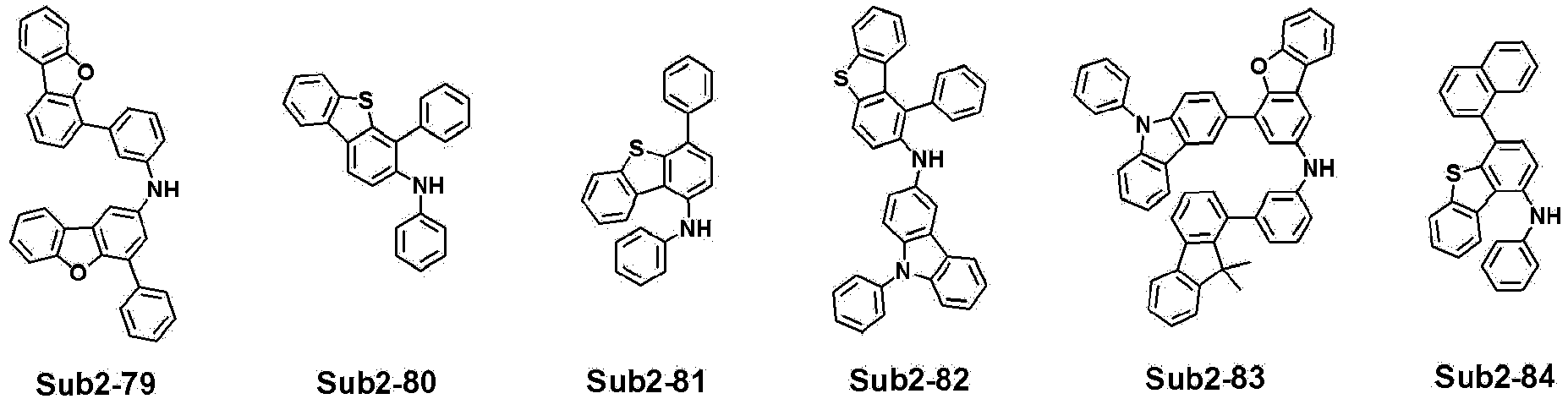


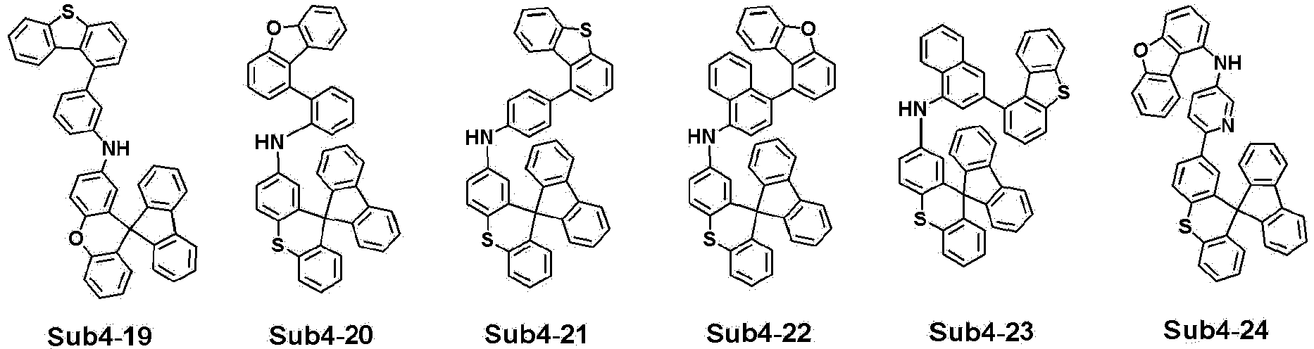


Table 2 compound FD-MS compound FD-MS Sub2-1 m/z=335.13(C24H17NO=335.41) Sub2-2 m/z=427.19(C31H25NO=427.55) Sub2-3 m/z=561.21(C42H27NO=561.68) Sub2-4 m/z=461.18(C34H23NO=461.56) Sub2-5 m/z=461.18(C34H23NO=461.56) Sub2-6 m/z=435.16(C24H17NO=435.53) Sub2-7 m/z=335.13(C24H17NO=335.41) Sub2-8 m/z=335.13(C32H21NO=335.41) Sub2-9 m/z=527.22(C39H29NO=527.67) Sub2-10 m/z=511.19(C38H25NO=511.62) Sub2-11 m/z=487.19(C36H25NO=487.60) Sub2-12 m/z=537.21(C40H27NO=537.66) Sub2-13 m/z=435.16(C32H21NO=435.53) Sub2-14 m/z=336.13(C23H16N2O=336.39) Sub2-15 m/z=452.15(C31H20N2O2=452.51) Sub2-16 m/z=500.19(C36H24N2O=500.60) Sub2-17 m/z=465.20(C34B19D4NO=465.59) Sub2-18 m/z=482.11(C31H18N2O2S=482.56) Sub2-19 m/z=567.17(C40H25NOS=567.71) Sub2-20 m/z=351.11(C24H17NS=351.47) Sub2-21 m/z=475.14(C34B21NS=475.61) Sub2-22 m/z=477.16(C34H23NS=477.63) Sub2-23 m/z=577.19(C42H27NS=577.75) Sub2-24 m/z=477.16(C34H23NS=477.63) Sub2-25 m/z=467.17(C33H25NS=467.63) Sub2-26 m/z=427.14(C30H21NS=427.57) Sub2-27 m/z=441.12(C30H19NOS=441.55) Sub2-28 m/z=427.14(C30H21NS=427.57) Sub2-29 m/z=457.10(C30H19NS2=457.61) Sub2-30 m/z=527.17(C38H25NS=527.69) Sub2-31 m/z=517.15(C36H23NOS=517.65) Sub2-32 m/z=352.10(C23H16N2S=352.46) Sub2-33 m/z=451.14(C32H21NS=451.59) Sub2-34 m/z=553.19(C40H27NS=553.72) Sub2-35 m/z=503.17(C36H25NS=503.66) Sub2-36 m/z=451.14(C32B21NS=451.59) Sub2-37 m/z=592.20(C42H28N2S=592.76) Sub2-38 m/z=583.14(C40H25NS2=583.77) Sub2-39 m/z=385.15(C28H19NO=385.47) Sub2-40 m/z=352.10(C23H16N2S=352.46) Sub2-41 m/z=401.12(C28H19NS=401.53) Sub2-42 m/z=477.16(C34H23NS=477.63) Sub2-43 m/z=507.11(C34H21NS2=507.67) Sub2-44 m/z=553.19(C40H27NS=553.72) Sub2-45 m/z=527.17(C38H25NS=527.69) Sub2-46 m/z=517.15(C36H23NOS=517.65) Sub2-47 m/z=498.09(C31H18N2OS2=498.62) Sub2-48 m/z=427.14(C30H21NS=427.57) Sub2-49 m/z=468.13(C31H20N2OS=468.57) Sub2-50 m/z=385.15(C28H19NO=385.47) Sub2-51 m/z=441.12(C30H19NOS=441.55) Sub2-52 m/z=367.14(C25H21NS=367.51) Sub2-53 m/z=577.24(C43H31NO=577.73) Sub2-54 m/z=351.16(C25H21NO=351.45) Sub2-55 m/z=435.16(C32H21NO=435.53) Sub2-56 m/z=451.19(C33H25NO=451.57) Sub2-57 m/z=427.19(C31H25NO=427.55) Sub2-58 m/z=441.12(C30H19NOS=441.55) Sub2-59 m/z=477.21(C35H27NO=477.61) Sub2-60 m/z=528.22(C38H28N2O=528.66) Sub2-61 m/z=375.13(C26H17NO2=375.43) Sub2-62 m/z=609.25(C44H35NS=609.83) Sub2-63 m/z=533.18(C37H27NOS=533.69) Sub2-64 m/z=507.17(C35H25NOS=507.65) Sub2-65 m/z=572.16(C38H24N2O2S=572.68) Sub2-66 m/z=391.10(C26H17NOS=391.49) Sub2-67 m/z=724.25(C51H36N2OS=724.92) Sub2-68 m/z=527.22(C39H29NO=527.67) Sub2-69 m/z=441.12(C30H19NOS=441.55) Sub2-70 m/z=493.19(C35H27NS=493.67) Sub2-71 m/z=467.17(C33H25NS=467.63) Sub2-72 m/z=556.18(C38H24N2O3=556.62) Sub2-73 m/z=475.16(C34B21NO2=475.55) Sub2-74 m/z=567.22(C41H29NO2=567.69) Sub2-75 m/z=627.26(C47H33NO=627.79) Sub2-76 m/z=527.22(C39H29NO=527.67) Sub2-77 m/z=335.13(C24H17NO=335.41) Sub2-78 m/z=467.17(C33H25NS=467.63) Sub2-79 m/z=501.17(C36H23NO2=501.59) Sub2-80 m/z=351.11(C24H17NS=351.47) Sub2-81 m/z=351.11(C24H17NS=351.47) Sub2-82 m/z=516.17(C36H24N2S=516.66) Sub2-83 m/z=708.31(C52H40N2O=708.91) Sub2-84 m/z=401.12(C28H19NS=401.53) Sub2-85 m/z=401.12(C28H19NS=401.53) Sub2-86 m/z=351.11(C24H17NS=351.47) Sub2-87 m/z=518.18(C36H26N2S=518.68) Sub2-88 m/z=427.14(C30H21NS=427.57) Sub2-89 m/z=461.18(C34H23NO=461.56) Sub2-90 m/z=461.18(C34H23NO=461.56) Sub2-91 m/z=335.13(C24H17NO=335.41) Sub2-92 m/z=561.21(C42H27NO=561.68) Sub2-93 m/z=461.18(C34H23NO=461.56) Sub2-94 m/z=353.12(C24H16FNO=353.40) Sub2-95 m/z=391.19(C28H25NO=391.51) Sub2-96 m/z=259.10(C18H13NO=259.31) Sub2-97 m/z=275.08(C18H13NS=275.37) Sub3-1 m/z=375.16(C27H21NO=375.47) Sub3-2 m/z=375.16(C27H21NO=375.47) Sub3-3 m/z=375.16(C27H21NO=375.47) Sub3-4 m/z=391.14(C27H21NS=391.53) Sub3-5 m/z=499.19(C37H25NO=499.61) Sub3-6 m/z=499.19(C37H25NO=499.61) Sub3-7 m/z=499.19(C37H25NO=499.61) Sub3-8 m/z=499.19(C37H25NO=499.61) Sub3-9 m/z=515.17(C37H25NS=515.67) Sub3-10 m/z=497.18(C37H23NO=497.60) Sub3-11 m/z=513.16(C37H23NS=513.66) Sub3-12 m/z=451.19(C33H25NO=451.57) Sub3-13 m/z=467.17(C33H25NS=467.63) Sub3-14 m/z=451.19(C33H25NO=451.57) Sub3-15 m/z=467.17(C33H25NS=467.63) Sub3-16 m/z=451.19(C33H25NO=451.57) Sub3-17 m/z=467.17(C33H25NS=467.63) Sub3-18 m/z=451.19(C33H25NO=451.57) Sub3-19 m/z=451.19(C33H25NO=451.57) Sub3-20 m/z=451.19(C33H25NO=451.57) Sub3-21 m/z=451.19(C33H25NO=451.57) Sub3-22 m/z=467.17(C33H25NS=467.63) Sub3-23 m/z=467.17(C33H25NS=467.63) Sub3-24 m/z=467.17(C33H25NS=467.63) Sub3-25 m/z=501.21(C37H27NO=501.63) Sub3-26 m/z=517.19(C37H27NS=517.69) Sub3-27 m/z=501.21(C37H27NO=501.63) Sub3-28 m/z=517.19(C37H27NS=517.69) Sub3-29 m/z=501.21(C37H27NO=501.63) Sub3-30 m/z=517.19(C37H27NS=517.69) Sub3-31 m/z=452.19(C32H24N2O=452.56) Sub3-32 m/z=583.23(C42H33NS=583.79) Sub3-33 m/z=525.21(C39H27NO=525.65) Sub3-34 m/z=519.20(C37H21D4NS=519.70) Sub3-35 m/z=527.22(C39H29NO=527.67) Sub3-36 m/z=543.20(C39H29NS=543.73) Sub3-37 m/z=527.22(C39H29NO=527.67) Sub3-38 m/z=543.20(C39H29NS=543.73) Sub3-39 m/z=543.20(C39H29NS=543.73) Sub3-40 m/z=527.22(C39H29NO=527.67) Sub3-41 m/z=527.22(C39H29NO=527.67) Sub3-42 m/z=527.22(C39H29NO=527.67) Sub3-43 m/z=543.20(C39H29NS=543.73) Sub3-44 m/z=543.20(C39H29NS=543.73) Sub3-45 m/z=452.19(C32H24N2O=452.56) Sub3-46 m/z=441.16(C31H23NS=441.59) Sub3-47 m/z=441.16(C31H23NS=441.59) Sub3-48 m/z=425.18(C31H23NO=425.53) Sub3-49 m/z=425.18(C31H23NO=425.53) Sub3-50 m/z=467.17(C33H25NS=467.63) Sub3-51 m/z=577.24(C43H31NO=577.73) Sub3-52 m/z=573.21(C43H27NO=573.70) Sub3-53 m/z=497.18(C37H23NO=497.60) Sub3-54 m/z=497.18(C37H23NO=497.60) Sub3-55 m/z=513.16(C37H23NS=513.66) Sub3-56 m/z=441.16(C31H23NS=441.59) Sub3-57 m/z=549.21(C41H27NO=549.67) Sub4-1 m/z=513.17(C37H23NO2=513.60) Sub4-2 m/z=513.17(C37H23NO2=513.60) Sub4-3 m/z=513.17(C37H23NO2=513.60) Sub4-4 m/z=513.17(C37H23NO2=513.60) Sub4-5 m/z=579.17(C41H25NOS=579.72) Sub4-6 m/z=531.16(C37H22FNO3=531.59) Sub4-7 m/z=563.19(C41H25NO2=563.66) Sub4-8 m/z=665.24(C49H31NO2=665.79) Sub4-9 m/z=529.15(C37H23NOS=529.66) Sub4-10 m/z=529.15(C37H23NOS=529.66) Sub4-11 m/z=529.15(C37H23NOS=529.66) Sub4-12 m/z=529.15(C37H23NOS=529.66) Sub4-13 m/z=529.15(C37H23NOS=529.66) Sub4-14 m/z=529.15(C37H23NOS=529.66) Sub4-15 m/z=529.15(C37H23NOS=529.66) Sub4-16 m/z=529.15(C37H23NOS=529.66) Sub4-17 m/z=545.13(C37H23NS2=545.72) Sub4-18 m/z=589.20(C43H37NO2=589.69) Sub4-19 m/z=605.18(C43H27NOS=605.76) Sub4-20 m/z=605.18(C43H27NOS=605.76) Sub4-21 m/z=621.16(C43H27NS2=621.82) Sub4-22 m/z=655.20(C47H29NOS=655.82) Sub4-23 m/z=671.17(C47H29NS2=671.88) Sub4-24 m/z=606.18(C42H26N2OS=606.74) Sub4-25 m/z=622.15(C42H26N2S2=622.80) Sub4-26 m/z=589.20(C43H27NO2=589.69) Sub4-27 m/z=605.18(C43H27NOS=605.76) Sub4-28 m/z=589.20(C43H27NO2=589.69) Sub4-29 m/z=605.18(C43H27NOS=605.76) Sub4-30 m/z=605.18(C43H27NOS=605.76) Sub4-31 m/z=621.16(C43H27NS2=621.82) Sub4-32 m/z=563.19(C41H25NO2=563.66) Sub4-33 m/z=595.14(C41H25NS2=595.78) Sub4-34 m/z=579.17(C41H25NOS=579.72) Sub4-35 m/z=605.18(C43H27NOS=605.76) Sub4-36 m/z=671.17(C47H29NS2=671.88) Sub4-37 m/z=665.24(C49H31NO2=665.79) Sub4-38 m/z=549.15(C37H19D4NS2=549.74) Sub4-39 m/z=665.24(C49H31NO2=665.79) Sub4-40 m/z=589.20(C43H27NO2=589.69) Sub4-41 m/z=671.17(C47H29NS2=671.88) Sub4-42 m/z=595.14(C41H25NS2=595.78) Sub4-43 m/z=595.14(C41H25NS2=595.78) Sub4-44 m/z=563.19(C41H25NO2=563.66) -

- Sub1-1 (9.5 g, 25.9 mmol)and Sub4-3 (13.3 g, 25.9 mmol), Pd2(dba)3 (0.7 g, 0.8 mmol), NaOt-Bu (7.5 g, 77.7 mmol), anhydrous Toluene (200 mL), P(t-Bu)3 (50wt% Sol.) (0.6 mL, 0.8 mmol) were obtained 18.1 g (83% yield) of P2-3 using the synthesis method of P-1.
- The FD-MS values of compounds P2-1 to P2-55 of the present invention prepared according to the synthesis example as described above are shown in Table 3.
Table 3 Compound FD-MS compound FD-MS P2-1 m/z=843.28(C62H37NO3=843.98) P2-2 m/z=843.28(C62H37NO3=843.98) P2-3 m/z=843.28(C62H37NO3=843.98) P2-4 m/z=843.28(C62H37NO3=843.98) P2-5 m/z=909.27(C66H39NO2S=910.10) P2-6 m/z=861.27(C62H36FNO3=861.97) P2-7 m/z=893.29(C66H39NO3=894.04) P2-8 m/z=995.34(C74H45NO3=996.18) P2-9 m/z=859.25(C62H37NO2S=860.04) P2-10 m/z=859.25(C62H37NO2S=860.04) P2-11 m/z=859.25(C62H37NO2S=860.04) P2-12 m/z=859.25(C62H37NO2S=860.04) P2-13 m/z=859.25(C62H37NO2S=860.04) P2-14 m/z=859.25(C62H37NO2S=860.04) P2-15 m/z=859.25(C62H37NO2S=860.04) P2-16 m/z=859.25(C62H37NO2S=860.04) P2-17 m/z=875.23(C62H37NOS2=876.10) P2-18 m/z=875.23(C62H37NOS2=876.1) P2-19 m/z=891.21(C62H37NS3=892.17) P2-20 m/z=919.31(C68H41NO3=920.08) P2-21 m/z=935.29(C68H41NO2S=936.14) P2-22 m/z=951.26(C68H41NOS2=952.20) P2-23 m/z=967.24(C69H41NS3=968.26) P2-24 m/z=985.30(C72H43NO2S=986.20) P2-25 m/z=1001.28(C72H43NOS2=1002.26) P2-26 m/z=952.26(C67H40N2OS2=953.19) P2-27 m/z=952.26(C67H40N2OS2=953.19) P2-28 m/z=919.31(C68H41NO3=920.08) P2-29 m/z=935.29(C68H41NO2S=936.14) P2-30 m/z=919.31(C68H41NO3=920.08) P2-31 m/z=935.29(C68H41NO2S=936.14) P2-32 m/z=935.29(C68H41NO2S=936.14) P2-33 m/z=967.24(C68H41NS3=968.26) P2-34 m/z=900.23(C63H36N2OS2=901.11) P2-35 m/z=901.25(C64H39NOS2=902.14) P2-36 m/z=893.29(C66H39NO3=894.04) P2-37 m/z=941.22(C66H39NS3=942.23) P2-38 m/z=909.27(C66H39NO2S=910.10) P2-39 m/z=919.31(C68H41NO3=920.08) P2-40 m/z=941.22(C66H39NS3=942.23) P2-41 m/z=909.27(C66H39NO2S=910.1) P2-42 m/z=893.29(C66H39NO3=894.04) P2-43 m/z=941.22(C66H39NS3=942.23) P2-44 m/z=909.27(C66H39NO2S=910.10) P2-45 m/z=893.29(C66H39NO3=894.04) P2-46 m/z=951.26(C68H41NOS2=952.2) P2-47 m/z=1017.26(C72H43NS3=1018.32) P2-48 m/z=995.34(C74H45NO3=996.18) P2-49 m/z=895.23(C62H33D4NS3=896.19) P2-50 m/z=995.34(C74H45NO3=996.18) P2-51 m/z=995.34(C74H45NO3=996.18) P2-52 m/z=1093.29(C78H47NS3=1094.42) P2-53 m/z=975.26(C70H41NOS2=976.22) P2-54 m/z=991.24(C70H41NS3=992.29) P2-55 m/z=943.31(C70H41NO3=944.10) - 2-TNATA was vacuum-deposited to a thickness of 60 nm on the ITO layer (anode) formed on the glass substrate to form a hole injection layer, and then NPB was vacuum-deposited to a thickness of 60 nm on the hole injection layer to form a hole transport layer. Then, after vacuum deposition of the compound P 2-1 of the present invention to a thickness of 20 nm on the hole transport layer to form an emitting auxiliary layer, and on the emitting auxiliary layer, CBP was used as a host material and tris(2-phenylpyridine)-iridium(hereinafter, Ir(ppy)3) was used as a dopant material, doped at a weight ratio of 95:5, and vacuum deposited to a thickness of 30 nm to form an emitting layer. Subsequently, BAlq was vacuum deposited to a thickness of 10 nm on the emitting layer to form a hole blocking layer, Bis(10-hydroxybenzo[h]quinolinato)beryllium (hereinafter, BeBq2) was vacuum deposited to a thickness of 40 nm on the hole blocking layer to form an electron transport layer. Thereafter, an electron injection layer was formed by depositing LiF, an alkali metal halide, to a thickness of 0.2 nm, and subsequently, Al was deposited to a thickness of 150 nm to form a cathode, thereby manufacturing an organic light emitting diode.
- An organic light emitting diode was manufactured in the same manner as in Example 1, except that the compound of the present invention described in Table 7 was used instead of the compound P2-1 as the emitting auxiliary layer material.
- An organic light emitting diode was manufactured in the same manner as in Example 36, except that Comparative Compound 2 and Comparative Compound 4 were used, respectively, instead of the compound P2-1 as the emitting auxiliary layer material.
-

- Electroluminescence (EL) characteristics were measured by PR-650 of photoresearch company by applying a forward bias direct current voltage to the organic light emitting diode prepared according to Examples 36 to 47 and Comparative Example 4 to 6 of the present invention, T95 life was measured through a life measurement equipment manufactured by McScience at a luminance of 5000 cd/m2, and the measurement results are shown in Table 4.
Table 4 compou nd Voltag e (V) Current Density (mA/cm2) Brightness (cd/m2) Efficiency (cd/A) Lifetim e T(95) CIE x y comparative example (4) compar ative compou nd 2 6.5 33.1 5000.0 15.1 80.4 0.32 0.64 comparative example (5) compar ative compou nd 3 6.3 24.9 5000.0 20.1 88.6 0.30 0.64 comparative example (6) compar at ive compou nd 4 5.9 19.3 5000.0 25.9 105.7 0.32 0.63 example(1) P2-1 5.1 10.6 5000.0 47.2 133.2 0.33 0.60 example(2) P2-3 5.1 10.3 5000.0 48.4 135.1 0.33 0.61 example(3) P2-7 5.3 11.2 5000.0 44.5 128.7 0.34 0.60 example(4) P2-12 5.2 10.7 5000.0 46.7 122.6 0.30 0.62 example(5) P2-14 5.1 11.3 5000.0 44.2 127.1 0.32 0.60 example(6) P2-22 5.1 11.2 5000.0 44.7 122.5 0.30 0.62 example(7) P2-28 5.2 10.8 5000.0 46.4 132.5 0.34 0.65 example(8) P2-37 5.4 12.8 5000.0 39.0 120.2 0.34 0.60 example(9) P2-39 5.3 12.7 5000.0 39.3 131.5 0.32 0.64 example(10) P2-40 5.4 12.9 5000.0 38.8 120.8 0.34 0.61 example(11) P2-46 5.3 11.1 5000.0 45.0 124.2 0.31 0.62 example(12) P2-50 5.2 12.2 5000.0 41.0 126.6 0.31 0.62 - As can be seen from the results in Table 4, when a green organic light emitting diode is manufactured using the material for an organic light emitting diode of the present invention as an emitting auxiliary layer material, compared to the comparative compound 4 to 6, and the driving voltage of the organic light emitting diode could be lowered and the efficiency and lifespan were significantly improved.
- First, the device result using Comparative Compound 3 with arylamine bonded at the 2 position of the xanthene core was slightly improved than Comparative Compound 2 with arylamine bonded at the 3 position of the xanthene core, and the device result of Comparative Compound 4 in which one more xanthene was bonded as a substituent of the amine group was improved compared to Comparative Examples 4 and 5.
- The compound of the present invention is a compound characterized in that an amine group is bonded to 2 position of the xanthene core, and as a substituent of the amine group bonded to the core, one is bonded with 1 position of the dibenzofuran or dibenzothiophene, and the other is bonded with xanthene one more, and it can be seen that the device results of Examples 1 to 12 made of the compounds of the present invention having such characteristics are remarkably excellent.
- It is suggested that the compounds of the present invention having a substituent at a specific bonding site may have significantly different chemical and physical properties from those of the Comparative Example compounds, thereby leading to improved device results.
- Additionally, referring to Table 5, which lists the HOMO values of Comparative Compound 4 and the compound of the present invention, it can be seen that the HOMO value of Compound P 2-3 of the present invention, in which an amine group is bonded to the 2 position of the core, and one more xanthene is bonded at the same time as 1 position of dibenzofuran as a substituent of the bonded amine group, is higher than that of Comparative Compound 4.
Table 5 Comparative compound 4 P2-3 HOMO (eV) -4.856 -4.788 - That is, it is judged that the compound of the present invention can more efficiently transport holes in the hole transport layer, as a result, it is believed that the charge balance of holes and electrons in the emitting layer is increased, thereby improving the driving voltage, efficiency, and lifespan of the entire device.
- In the case of the emitting auxiliary layer, it is necessary to grasp the correlation between the hole transport layer and the emitting layer (host), even if a similar core is used, it will be very difficult for a person skilled in the art to infer the characteristics exhibited in the emitting auxiliary layer in which the compound of the present invention is used.
- In addition, the device characteristics in which the compound of the present invention was applied to only one of the emitting auxiliary layers were described in the result of evaluation of manufacture of the element above, but it may be applied to a case where a hole transport layer or both a hole transport layer and an emitting auxiliary layer are formed by using the compound of the present invention.
- Although exemplary embodiments of the present invention have been described for illustrative purposes, those skilled in the art will appreciate that various modifications, additions and substitutions are possible, without departing from the scope of the invention as disclosed in the accompanying claims. Therefore, the embodiments disclosed in the present invention are intended to illustrate the scope of the technical idea of the present invention, and the scope of the present invention is not limited by said embodiments.
- According to the present invention, it is possible to manufacture an organic device having excellent device characteristics of high luminance, high light emission and long lifespan, and thus there is industrial applicability.
Claims (11)
- A compound represented by Formula 6-1
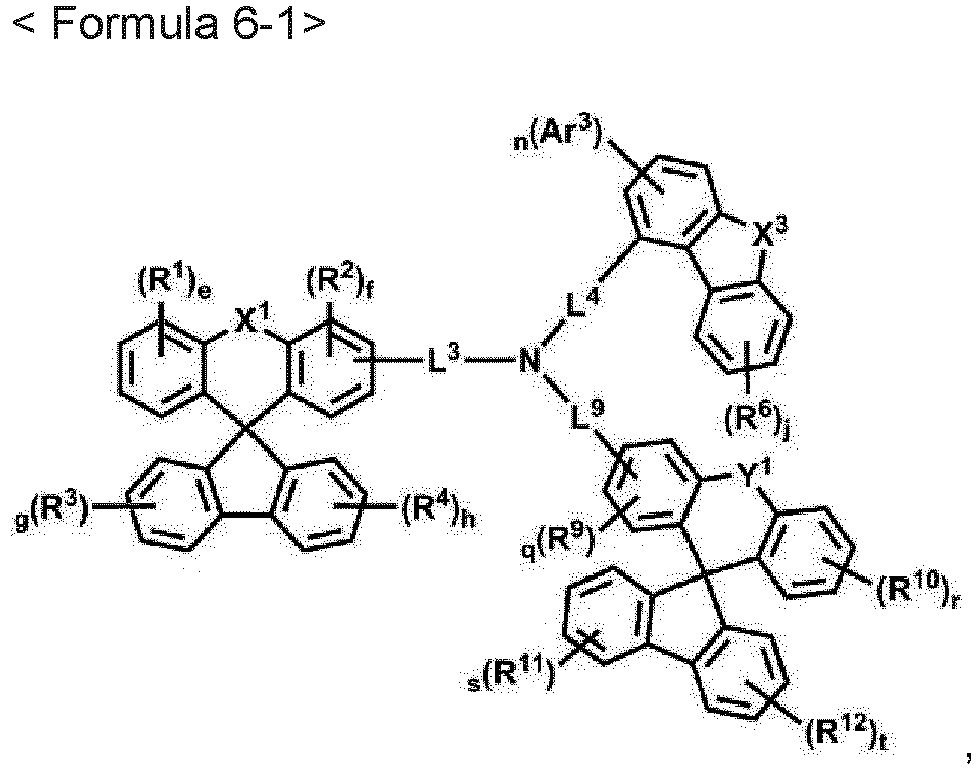 1) X1, and X3 are each independently O or S,2) is O or S,3) e, f, g, h, j, r, s and t are each independently an integer of 0 to 4, q is an integer of 0 to 3, wherein in case e, f, g, h, j, q, and r, are 2 or more, R1, R2, R3, R4, and R6 are each in plural being the same or different, and an adjacent plurality of R1 or a plurality of R2 or a plurality of R3 or a plurality of R4 or a plurality of R6 or a plurality of R9 or a plurality of R10 or a plurality of R11 or a plurality of R12 may be bonded to each other to form a ring,4) n is an integer of 0 to 3,5) L3, L4, and L9 are the same or different from each other, and are each independently selected from the group consisting of single bond; a C6-C60 arylene group; a fluorenylene group; a fused ring group of a C3-C60 aliphatic ring and a C6-C60 aromatic ring; a C2-C60 heterocyclic group;6) Ar3 is selected from the group consisting of hydrogen; deuterium; tritium; halogen; cyano group; nitro group; C6-C60 aryl group; a fluorenyl group; a C2-C60 heterocyclic group including at least one heteroatom of O, N, S, Si or P; a fused ring group of a C3-C60 aliphatic ring and a C6-C60 aromatic ring; C1-C50 alkyl group; C2-C20 alkenyl group; C2-C20 alkynyl group; C1-C30 alkoxyl group; C6-C30 aryloxy group; and -L'-N(Ra)(Rb);7) R1, R2, R3, R4, R6, R9, R10, R11 and R12 are the same or different from each other, and are each independently selected from the group consisting of hydrogen; deuterium; tritium; halogen; cyano group; nitro group; C6-C60 aryl group; a fluorenyl group; a C2-C60 heterocyclic group including at least one heteroatom of O, N, S, Si or P; a fused ring group of a C3-C60 aliphatic ring and a C6-C60 aromatic ring; C1-C50 alkyl group; C2-C20 alkenyl group; C2-C20 alkynyl group; C1-C30 alkoxyl group; C6-C30 aryloxy group; and -L'-N(Ra)(Rb);8) wherein L' is selected from the group consisting of a single bond; a C6-C60 arylene group; a fluorenylene group; C3-C60 aliphatic ring; a C2-C60 heterocyclic group including at least one heteroatom of O, N, S, Si or P; a combination thereof; wherein Ra and Rb are each independently selected from the group consisting of a C6-C60 aryl group; a fluorenyl group; C3-C60 aliphatic ring; a C2-C60 heterocyclic group including at least one heteroatom of O, N, S, Si or P;9) wherein, the aryl group, arylene group, heterocyclic group, fluorenyl group, fluorenylene group, fused ring group, alkyl group, alkenyl group, alkoxy group and aryloxy group may be substituted with one or more substituents selected from the group consisting of deuterium; halogen; silane group; siloxane group; boron group; germanium group; cyano group; nitro group; C1-C20 alkylthio group; C1-C20 alkoxyl group; C1-C20 alkyl group; C2-C20 alkenyl group; C2-C20 alkynyl group; C6-C25 aryl group; C6-C25 aryl group substituted with deuterium; a fluorenyl group; C2-C20 heterocyclic group; C3-C20 cycloalkyl group; C7-C20 arylalkyl group; C8-C20 arylalkenyl group; and -L'-N(Ra)(Rb); wherein the substituents may be bonded to each other to form a saturated or unsaturated ring, wherein the term 'ring' means a C3-C60 aliphatic ring, a C6-C60 aromatic ring, a C2-C60 heterocyclic group, a fused ring formed by combination thereof.
 - The compound according to claim 1, wherein Formula 6-1 is represented by Formula 6-2 or Formula 6-3,


 1) X1, X3, Y1, R1, R2, R3, R4, R6, R9, R10, R11, R12, L3, L4, Ar3, e, f, g, h, j, n, q, r, s, and t, are the same as defined in claim 1.
 - The compound according to claim 1, wherein Formula 6-1 is represented by any one of the following compounds:


- An organic electronic element comprising an anode, a cathode, and an organic material layer formed between the anode and the cathode, wherein the organic material layer comprises a single compound or 2 or more compounds represented by Formula 6-1 of claim 1.
- The organic electronic element of claim 4, wherein the organic material layer comprises at least one of a hole injection layer, a hole transport layer, an emitting auxiliary layer, an emitting layer, an electron transport auxiliary layer, an electron transport layer, and an electron injection layer.
- The organic electronic element of claim 4, wherein the organic material layer is an emitting auxiliary layer.
- The organic electronic element of claim 4, further comprising a light efficiency enhancing layer formed on at least one surface of the anode and the cathode opposite to the organic material layer.
- The organic electronic element of claim 4, wherein the organic material layer comprises 2 or more stacks including a hole transport layer, an emitting layer, and an electron transport layer sequentially formed on the anode.
- The organic electronic element of claim 8, wherein the organic material layer further comprises a charge generation layer formed between the 2 or more stacks.
- A display device comprising the organic electronic element of claim 4; and a control unit for driving the display device.
- The display device according to claim 10, wherein the organic electronic element is at least one of an OLED, an organic solar cell, an organic photo conductor(OPC), organic transistor(organic TFT) and an element for monochromic or white illumination.
Applications Claiming Priority (4)
| Application Number | Priority Date | Filing Date | Title |
|---|---|---|---|
| KR20190148780 | 2019-11-19 | ||
| KR1020200102536A KR102924500B1 (en) | 2019-11-19 | 2020-08-14 | Compound for organic electronic element, organic electronic element using the same, and an electronic device thereof |
| PCT/KR2020/016272 WO2021101247A1 (en) | 2019-11-19 | 2020-11-18 | Compound for organic electrical element, organic electrical element using same and electronic device thereof |
| EP20890898.8A EP4039683A4 (en) | 2019-11-19 | 2020-11-18 | Compound for organic electrical element, organic electrical element using same and electronic device thereof |
Related Parent Applications (1)
| Application Number | Title | Priority Date | Filing Date |
|---|---|---|---|
| EP20890898.8A Division EP4039683A4 (en) | 2019-11-19 | 2020-11-18 | Compound for organic electrical element, organic electrical element using same and electronic device thereof |
Publications (3)
| Publication Number | Publication Date |
|---|---|
| EP4269406A2 EP4269406A2 (en) | 2023-11-01 |
| EP4269406A3 EP4269406A3 (en) | 2023-11-08 |
| EP4269406B1 true EP4269406B1 (en) | 2024-07-10 |
Family
ID=75980975
Family Applications (3)
| Application Number | Title | Priority Date | Filing Date |
|---|---|---|---|
| EP20890898.8A Pending EP4039683A4 (en) | 2019-11-19 | 2020-11-18 | Compound for organic electrical element, organic electrical element using same and electronic device thereof |
| EP23160806.8A Active EP4269406B1 (en) | 2019-11-19 | 2020-11-18 | Compound for organic electrical element, organic electrical element using same and electronic device thereof |
| EP23160809.2A Pending EP4215528A1 (en) | 2019-11-19 | 2020-11-18 | Compound for organic electrical element, organic electrical element using same and electronic device thereof |
Family Applications Before (1)
| Application Number | Title | Priority Date | Filing Date |
|---|---|---|---|
| EP20890898.8A Pending EP4039683A4 (en) | 2019-11-19 | 2020-11-18 | Compound for organic electrical element, organic electrical element using same and electronic device thereof |
Family Applications After (1)
| Application Number | Title | Priority Date | Filing Date |
|---|---|---|---|
| EP23160809.2A Pending EP4215528A1 (en) | 2019-11-19 | 2020-11-18 | Compound for organic electrical element, organic electrical element using same and electronic device thereof |
Country Status (4)
| Country | Link |
|---|---|
| US (1) | US12274163B2 (en) |
| EP (3) | EP4039683A4 (en) |
| CN (4) | CN117567443A (en) |
| WO (1) | WO2021101247A1 (en) |
Families Citing this family (7)
| Publication number | Priority date | Publication date | Assignee | Title |
|---|---|---|---|---|
| KR102853917B1 (en) * | 2020-01-20 | 2025-09-02 | 덕산네오룩스 주식회사 | Compound for organic electronic element, organic electronic element using the same, and an electronic device thereof |
| US11925116B2 (en) * | 2020-10-26 | 2024-03-05 | Duk San Neolux Co., Ltd. | Compound for organic electronic element, organic electronic element using the same, and an electronic device thereof |
| WO2022108141A1 (en) * | 2020-11-18 | 2022-05-27 | 엘티소재주식회사 | Compound and organic light-emitting device comprising same |
| CN115028540B (en) * | 2021-04-02 | 2023-10-10 | 陕西莱特光电材料股份有限公司 | Organic electroluminescent material, electronic element and electronic device |
| KR102374470B1 (en) * | 2021-07-21 | 2022-03-15 | 덕산네오룩스 주식회사 | Compound for organic electronic element, organic electronic element using the same, and an electronic device thereof |
| CN115626915A (en) * | 2022-11-14 | 2023-01-20 | 吉林奥来德光电材料股份有限公司 | Light-emitting auxiliary material and its preparation method, light-emitting device and light-emitting device |
| CN118324733A (en) * | 2024-06-17 | 2024-07-12 | 浙江华显光电科技有限公司 | An organic compound, an OLED having the same, and an organic light-emitting device |
Family Cites Families (24)
| Publication number | Priority date | Publication date | Assignee | Title |
|---|---|---|---|---|
| EP1804309B1 (en) * | 2005-12-23 | 2008-07-23 | Novaled AG | Electronic device with a layer structure of organic layers |
| EP3378857B1 (en) * | 2012-11-12 | 2021-03-24 | Merck Patent GmbH | Materials for electronic devices |
| KR101604642B1 (en) | 2013-06-17 | 2016-03-22 | 덕산네오룩스 주식회사 | Compound Containing Five Membered heterocyclic compound, And Organic Electronic Element Using The Same, Terminal Thereof |
| KR101530886B1 (en) | 2015-02-09 | 2015-06-24 | 덕산네오룩스 주식회사 | Compound for organic electronic element, organic electronic element using the same, and an electronic device thereof |
| KR101822477B1 (en) * | 2015-03-16 | 2018-01-26 | 덕산네오룩스 주식회사 | Compound for organic electric element, organic electric element comprising the same and electronic device thereof |
| KR101579490B1 (en) | 2015-09-17 | 2015-12-22 | 덕산네오룩스 주식회사 | Compound for organic electronic element, organic electronic element using the same, and an electronic device thereof |
| KR101781739B1 (en) * | 2015-10-07 | 2017-09-25 | 주식회사 엘지화학 | New compound and organic light emitting device comprising the same |
| CN105778891B (en) * | 2016-03-11 | 2019-03-19 | 中节能万润股份有限公司 | Organic photoelectrical material, preparation method and the organic electroluminescence device including the organic material |
| CN105906640B (en) | 2016-05-12 | 2018-03-30 | 中节能万润股份有限公司 | A kind of preparation method of blue light dopant material |
| KR101910498B1 (en) | 2016-06-08 | 2018-10-22 | (주)씨엠디엘 | The novel organic electroluminescent compounds and organic electroluminescent device including the same |
| KR102639569B1 (en) | 2016-06-20 | 2024-02-23 | 삼성디스플레이 주식회사 | Condensed compound and organic light emitting device comprising the same |
| TWI764942B (en) * | 2016-10-10 | 2022-05-21 | 德商麥克專利有限公司 | Electronic device |
| KR20180112962A (en) | 2017-04-05 | 2018-10-15 | (주)피엔에이치테크 | An electroluminescent compound and an electroluminescent device comprising the same |
| KR102088180B1 (en) * | 2017-08-03 | 2020-03-12 | 이데미쓰 고산 가부시키가이샤 | Compounds, materials for organic electroluminescent devices, organic electroluminescent devices, and electronic devices |
| KR102507585B1 (en) | 2017-11-27 | 2023-03-09 | 에스에프씨 주식회사 | Novel organic compounds derivatives and organic light-emitting diode therewith |
| CN109867652B (en) | 2017-12-04 | 2023-11-10 | Cmdl有限公司 | Novel organic compound and organic electroluminescent device comprising the same |
| KR102607902B1 (en) | 2018-05-28 | 2023-11-30 | 삼성디스플레이 주식회사 | Organic electroluminescence device and monoamine compound for organic electroluminescence device |
| KR102288755B1 (en) | 2018-06-12 | 2021-08-10 | 주식회사 엘지화학 | Novel compound and organic light emittng device comprising the same |
| KR102100581B1 (en) * | 2019-01-30 | 2020-04-14 | 두산솔루스 주식회사 | Organic light-emitting compound and organic electroluminescent device using the same |
| KR102475856B1 (en) * | 2019-02-15 | 2022-12-08 | 주식회사 엘지화학 | Novel compound and organic light emitting device comprising the same |
| WO2020218680A1 (en) * | 2019-04-25 | 2020-10-29 | 두산솔루스 주식회사 | Organic compound and organic electroluminescent diode using same |
| KR102820538B1 (en) * | 2019-07-10 | 2025-06-13 | 덕산네오룩스 주식회사 | Compound for organic electronic element, organic electronic element using the same, and an electronic device thereof |
| US12108671B2 (en) | 2019-11-01 | 2024-10-01 | Duk San Neolux Co., Ltd. | Organic electric element comprising a plurality of emission-auxiliary layers and electronic device comprising it |
| CN110835328A (en) * | 2019-11-18 | 2020-02-25 | 苏州久显新材料有限公司 | Spirobenzofluorenone derivatives and electronic devices |
-
2020
- 2020-11-18 CN CN202311572177.4A patent/CN117567443A/en active Pending
- 2020-11-18 CN CN202410728265.7A patent/CN118745171A/en active Pending
- 2020-11-18 EP EP20890898.8A patent/EP4039683A4/en active Pending
- 2020-11-18 EP EP23160806.8A patent/EP4269406B1/en active Active
- 2020-11-18 US US17/756,193 patent/US12274163B2/en active Active
- 2020-11-18 WO PCT/KR2020/016272 patent/WO2021101247A1/en not_active Ceased
- 2020-11-18 CN CN202080080199.7A patent/CN114728948B/en active Active
- 2020-11-18 EP EP23160809.2A patent/EP4215528A1/en active Pending
- 2020-11-18 CN CN202311571830.5A patent/CN117567445A/en active Pending
Also Published As
| Publication number | Publication date |
|---|---|
| CN114728948A (en) | 2022-07-08 |
| CN114728948B (en) | 2024-12-03 |
| CN117567443A (en) | 2024-02-20 |
| US20230040837A1 (en) | 2023-02-09 |
| CN118745171A (en) | 2024-10-08 |
| EP4039683A4 (en) | 2022-11-30 |
| CN117567445A (en) | 2024-02-20 |
| EP4215528A1 (en) | 2023-07-26 |
| EP4269406A2 (en) | 2023-11-01 |
| EP4039683A1 (en) | 2022-08-10 |
| EP4269406A3 (en) | 2023-11-08 |
| US12274163B2 (en) | 2025-04-08 |
| WO2021101247A1 (en) | 2021-05-27 |
Similar Documents
| Publication | Publication Date | Title |
|---|---|---|
| CN115380025B (en) | Compound for organic electric device, organic electric device using the compound, and electronic device including the organic electric device | |
| KR101498278B1 (en) | Compound for organic electronic element, organic electronic element using the same, and an electronic device thereof | |
| JP6302932B2 (en) | COMPOUND FOR ORGANIC ELECTRIC ELEMENT, ORGANIC ELECTRIC ELEMENT USING THE SAME, AND ELECTRONIC DEVICE THEREOF | |
| CN114728948B (en) | Compound for organic electronic element, organic electronic element using the compound, and electronic device thereof | |
| KR20160004513A (en) | Compound for organic electronic element, organic electronic element using the same, and an electronic device thereof | |
| KR20180011429A (en) | Compound for organic electric element, organic electric element comprising the same and electronic device thereof | |
| KR20160026136A (en) | Compound for organic electronic element, organic electronic element using the same, and an electronic device thereof | |
| KR101791023B1 (en) | Fused aromatic compound and organic electroluminescent devices comprising the same | |
| KR20190011463A (en) | Compound for organic electronic element, organic electronic element comprising the same, and electronic device thereof | |
| TWI662040B (en) | Polyheteroaromatic compound and organic electroluminescence device using the same | |
| KR20150016896A (en) | Organic electric element comprising compound for organic electric element and electronic device thereof | |
| KR20180105882A (en) | Compound for organic electric element, organic electric element comprising the same and electronic device thereof | |
| KR20160041391A (en) | Compound for organic electronic element, organic electronic element using the same, and an electronic device thereof | |
| KR20180133097A (en) | Compound for organic electric element, organic electric element comprising the same and electronic device thereof | |
| CN115777242A (en) | Organic electronic element containing compound for organic electronic element and electronic device thereof | |
| KR102554212B1 (en) | Compound for organic electronic element, organic electronic element comprising the same, and electronic device thereof | |
| US20170040546A1 (en) | Novel compound and organic electronic device using the same | |
| KR101950893B1 (en) | Compound for organic electronic element, organic electronic element usingthe same, and a electronic device thereof | |
| KR102488854B1 (en) | Compound for organic electronic element, organic electronic element comprising the same, and electronic device thereof | |
| KR102093186B1 (en) | Compound for organic electronic element, organic electronic element using the same, and an electronic device thereof | |
| KR20200060611A (en) | Compound for organic electronic element, organic electronic element using the same, and an electronic device thereof | |
| KR20160125022A (en) | Compound for organic electric element, organic electric element comprising the same and electronic device thereof | |
| CN116583507B (en) | Compound for organic electronic element, organic electronic element using the same, and electronic device using the same | |
| KR20190000162A (en) | Compound for organic electronic element, organic electronic element comprising the same, and electronic device thereof | |
| KR20210049544A (en) | Heterocyclic compound and organic light emitting device comprising same |
Legal Events
| Date | Code | Title | Description |
|---|---|---|---|
| PUAI | Public reference made under article 153(3) epc to a published international application that has entered the european phase |
Free format text: ORIGINAL CODE: 0009012 |
|
| STAA | Information on the status of an ep patent application or granted ep patent |
Free format text: STATUS: REQUEST FOR EXAMINATION WAS MADE |
|
| REG | Reference to a national code |
Ref country code: DE Ref legal event code: R079 Free format text: PREVIOUS MAIN CLASS: C07D0405120000 Ipc: C07D0409120000 Ref country code: DE Ref legal event code: R079 Ref document number: 602020033949 Country of ref document: DE Free format text: PREVIOUS MAIN CLASS: C07D0405120000 Ipc: C07D0409120000 |
|
| PUAL | Search report despatched |
Free format text: ORIGINAL CODE: 0009013 |
|
| 17P | Request for examination filed |
Effective date: 20230315 |
|
| AC | Divisional application: reference to earlier application |
Ref document number: 4039683 Country of ref document: EP Kind code of ref document: P |
|
| AK | Designated contracting states |
Kind code of ref document: A2 Designated state(s): AL AT BE BG CH CY CZ DE DK EE ES FI FR GB GR HR HU IE IS IT LI LT LU LV MC MK MT NL NO PL PT RO RS SE SI SK SM TR |
|
| AK | Designated contracting states |
Kind code of ref document: A3 Designated state(s): AL AT BE BG CH CY CZ DE DK EE ES FI FR GB GR HR HU IE IS IT LI LT LU LV MC MK MT NL NO PL PT RO RS SE SI SK SM TR |
|
| RIC1 | Information provided on ipc code assigned before grant |
Ipc: C07D 417/14 20060101ALI20231005BHEP Ipc: C07D 413/14 20060101ALI20231005BHEP Ipc: C07D 411/14 20060101ALI20231005BHEP Ipc: C07D 407/14 20060101ALI20231005BHEP Ipc: C07D 407/12 20060101ALI20231005BHEP Ipc: C07D 409/14 20060101ALI20231005BHEP Ipc: C07D 409/12 20060101AFI20231005BHEP |
|
| P01 | Opt-out of the competence of the unified patent court (upc) registered |
Effective date: 20231120 |
|
| STAA | Information on the status of an ep patent application or granted ep patent |
Free format text: STATUS: EXAMINATION IS IN PROGRESS |
|
| 17Q | First examination report despatched |
Effective date: 20240118 |
|
| GRAP | Despatch of communication of intention to grant a patent |
Free format text: ORIGINAL CODE: EPIDOSNIGR1 |
|
| STAA | Information on the status of an ep patent application or granted ep patent |
Free format text: STATUS: GRANT OF PATENT IS INTENDED |
|
| INTG | Intention to grant announced |
Effective date: 20240425 |
|
| GRAS | Grant fee paid |
Free format text: ORIGINAL CODE: EPIDOSNIGR3 |
|
| GRAA | (expected) grant |
Free format text: ORIGINAL CODE: 0009210 |
|
| STAA | Information on the status of an ep patent application or granted ep patent |
Free format text: STATUS: THE PATENT HAS BEEN GRANTED |
|
| AC | Divisional application: reference to earlier application |
Ref document number: 4039683 Country of ref document: EP Kind code of ref document: P |
|
| AK | Designated contracting states |
Kind code of ref document: B1 Designated state(s): AL AT BE BG CH CY CZ DE DK EE ES FI FR GB GR HR HU IE IS IT LI LT LU LV MC MK MT NL NO PL PT RO RS SE SI SK SM TR |
|
| REG | Reference to a national code |
Ref country code: CH Ref legal event code: EP |
|
| REG | Reference to a national code |
Ref country code: DE Ref legal event code: R096 Ref document number: 602020033949 Country of ref document: DE |
|
| REG | Reference to a national code |
Ref country code: LT Ref legal event code: MG9D |
|
| REG | Reference to a national code |
Ref country code: NL Ref legal event code: MP Effective date: 20240710 |
|
| PG25 | Lapsed in a contracting state [announced via postgrant information from national office to epo] |
Ref country code: PT Free format text: LAPSE BECAUSE OF FAILURE TO SUBMIT A TRANSLATION OF THE DESCRIPTION OR TO PAY THE FEE WITHIN THE PRESCRIBED TIME-LIMIT Effective date: 20241111 |
|
| REG | Reference to a national code |
Ref country code: AT Ref legal event code: MK05 Ref document number: 1701979 Country of ref document: AT Kind code of ref document: T Effective date: 20240710 |
|
| PG25 | Lapsed in a contracting state [announced via postgrant information from national office to epo] |
Ref country code: NL Free format text: LAPSE BECAUSE OF FAILURE TO SUBMIT A TRANSLATION OF THE DESCRIPTION OR TO PAY THE FEE WITHIN THE PRESCRIBED TIME-LIMIT Effective date: 20240710 |
|
| PG25 | Lapsed in a contracting state [announced via postgrant information from national office to epo] |
Ref country code: PT Free format text: LAPSE BECAUSE OF FAILURE TO SUBMIT A TRANSLATION OF THE DESCRIPTION OR TO PAY THE FEE WITHIN THE PRESCRIBED TIME-LIMIT Effective date: 20241111 Ref country code: NL Free format text: LAPSE BECAUSE OF FAILURE TO SUBMIT A TRANSLATION OF THE DESCRIPTION OR TO PAY THE FEE WITHIN THE PRESCRIBED TIME-LIMIT Effective date: 20240710 |
|
| PG25 | Lapsed in a contracting state [announced via postgrant information from national office to epo] |
Ref country code: NO Free format text: LAPSE BECAUSE OF FAILURE TO SUBMIT A TRANSLATION OF THE DESCRIPTION OR TO PAY THE FEE WITHIN THE PRESCRIBED TIME-LIMIT Effective date: 20241010 |
|
| PG25 | Lapsed in a contracting state [announced via postgrant information from national office to epo] |
Ref country code: GR Free format text: LAPSE BECAUSE OF FAILURE TO SUBMIT A TRANSLATION OF THE DESCRIPTION OR TO PAY THE FEE WITHIN THE PRESCRIBED TIME-LIMIT Effective date: 20241011 Ref country code: FI Free format text: LAPSE BECAUSE OF FAILURE TO SUBMIT A TRANSLATION OF THE DESCRIPTION OR TO PAY THE FEE WITHIN THE PRESCRIBED TIME-LIMIT Effective date: 20240710 Ref country code: PL Free format text: LAPSE BECAUSE OF FAILURE TO SUBMIT A TRANSLATION OF THE DESCRIPTION OR TO PAY THE FEE WITHIN THE PRESCRIBED TIME-LIMIT Effective date: 20240710 |
|
| PG25 | Lapsed in a contracting state [announced via postgrant information from national office to epo] |
Ref country code: BG Free format text: LAPSE BECAUSE OF FAILURE TO SUBMIT A TRANSLATION OF THE DESCRIPTION OR TO PAY THE FEE WITHIN THE PRESCRIBED TIME-LIMIT Effective date: 20240710 |
|
| PG25 | Lapsed in a contracting state [announced via postgrant information from national office to epo] |
Ref country code: LV Free format text: LAPSE BECAUSE OF FAILURE TO SUBMIT A TRANSLATION OF THE DESCRIPTION OR TO PAY THE FEE WITHIN THE PRESCRIBED TIME-LIMIT Effective date: 20240710 |
|
| PG25 | Lapsed in a contracting state [announced via postgrant information from national office to epo] |
Ref country code: AT Free format text: LAPSE BECAUSE OF FAILURE TO SUBMIT A TRANSLATION OF THE DESCRIPTION OR TO PAY THE FEE WITHIN THE PRESCRIBED TIME-LIMIT Effective date: 20240710 Ref country code: IS Free format text: LAPSE BECAUSE OF FAILURE TO SUBMIT A TRANSLATION OF THE DESCRIPTION OR TO PAY THE FEE WITHIN THE PRESCRIBED TIME-LIMIT Effective date: 20241110 |
|
| PG25 | Lapsed in a contracting state [announced via postgrant information from national office to epo] |
Ref country code: HR Free format text: LAPSE BECAUSE OF FAILURE TO SUBMIT A TRANSLATION OF THE DESCRIPTION OR TO PAY THE FEE WITHIN THE PRESCRIBED TIME-LIMIT Effective date: 20240710 |
|
| PG25 | Lapsed in a contracting state [announced via postgrant information from national office to epo] |
Ref country code: ES Free format text: LAPSE BECAUSE OF FAILURE TO SUBMIT A TRANSLATION OF THE DESCRIPTION OR TO PAY THE FEE WITHIN THE PRESCRIBED TIME-LIMIT Effective date: 20240710 Ref country code: RS Free format text: LAPSE BECAUSE OF FAILURE TO SUBMIT A TRANSLATION OF THE DESCRIPTION OR TO PAY THE FEE WITHIN THE PRESCRIBED TIME-LIMIT Effective date: 20241010 |
|
| PG25 | Lapsed in a contracting state [announced via postgrant information from national office to epo] |
Ref country code: RS Free format text: LAPSE BECAUSE OF FAILURE TO SUBMIT A TRANSLATION OF THE DESCRIPTION OR TO PAY THE FEE WITHIN THE PRESCRIBED TIME-LIMIT Effective date: 20241010 Ref country code: PL Free format text: LAPSE BECAUSE OF FAILURE TO SUBMIT A TRANSLATION OF THE DESCRIPTION OR TO PAY THE FEE WITHIN THE PRESCRIBED TIME-LIMIT Effective date: 20240710 Ref country code: NO Free format text: LAPSE BECAUSE OF FAILURE TO SUBMIT A TRANSLATION OF THE DESCRIPTION OR TO PAY THE FEE WITHIN THE PRESCRIBED TIME-LIMIT Effective date: 20241010 Ref country code: LV Free format text: LAPSE BECAUSE OF FAILURE TO SUBMIT A TRANSLATION OF THE DESCRIPTION OR TO PAY THE FEE WITHIN THE PRESCRIBED TIME-LIMIT Effective date: 20240710 Ref country code: IS Free format text: LAPSE BECAUSE OF FAILURE TO SUBMIT A TRANSLATION OF THE DESCRIPTION OR TO PAY THE FEE WITHIN THE PRESCRIBED TIME-LIMIT Effective date: 20241110 Ref country code: HR Free format text: LAPSE BECAUSE OF FAILURE TO SUBMIT A TRANSLATION OF THE DESCRIPTION OR TO PAY THE FEE WITHIN THE PRESCRIBED TIME-LIMIT Effective date: 20240710 Ref country code: GR Free format text: LAPSE BECAUSE OF FAILURE TO SUBMIT A TRANSLATION OF THE DESCRIPTION OR TO PAY THE FEE WITHIN THE PRESCRIBED TIME-LIMIT Effective date: 20241011 Ref country code: FI Free format text: LAPSE BECAUSE OF FAILURE TO SUBMIT A TRANSLATION OF THE DESCRIPTION OR TO PAY THE FEE WITHIN THE PRESCRIBED TIME-LIMIT Effective date: 20240710 Ref country code: ES Free format text: LAPSE BECAUSE OF FAILURE TO SUBMIT A TRANSLATION OF THE DESCRIPTION OR TO PAY THE FEE WITHIN THE PRESCRIBED TIME-LIMIT Effective date: 20240710 Ref country code: BG Free format text: LAPSE BECAUSE OF FAILURE TO SUBMIT A TRANSLATION OF THE DESCRIPTION OR TO PAY THE FEE WITHIN THE PRESCRIBED TIME-LIMIT Effective date: 20240710 Ref country code: AT Free format text: LAPSE BECAUSE OF FAILURE TO SUBMIT A TRANSLATION OF THE DESCRIPTION OR TO PAY THE FEE WITHIN THE PRESCRIBED TIME-LIMIT Effective date: 20240710 |
|
| REG | Reference to a national code |
Ref country code: DE Ref legal event code: R097 Ref document number: 602020033949 Country of ref document: DE |
|
| PG25 | Lapsed in a contracting state [announced via postgrant information from national office to epo] |
Ref country code: SM Free format text: LAPSE BECAUSE OF FAILURE TO SUBMIT A TRANSLATION OF THE DESCRIPTION OR TO PAY THE FEE WITHIN THE PRESCRIBED TIME-LIMIT Effective date: 20240710 Ref country code: DK Free format text: LAPSE BECAUSE OF FAILURE TO SUBMIT A TRANSLATION OF THE DESCRIPTION OR TO PAY THE FEE WITHIN THE PRESCRIBED TIME-LIMIT Effective date: 20240710 Ref country code: RO Free format text: LAPSE BECAUSE OF FAILURE TO SUBMIT A TRANSLATION OF THE DESCRIPTION OR TO PAY THE FEE WITHIN THE PRESCRIBED TIME-LIMIT Effective date: 20240710 |
|
| PG25 | Lapsed in a contracting state [announced via postgrant information from national office to epo] |
Ref country code: EE Free format text: LAPSE BECAUSE OF FAILURE TO SUBMIT A TRANSLATION OF THE DESCRIPTION OR TO PAY THE FEE WITHIN THE PRESCRIBED TIME-LIMIT Effective date: 20240710 |
|
| PG25 | Lapsed in a contracting state [announced via postgrant information from national office to epo] |
Ref country code: CZ Free format text: LAPSE BECAUSE OF FAILURE TO SUBMIT A TRANSLATION OF THE DESCRIPTION OR TO PAY THE FEE WITHIN THE PRESCRIBED TIME-LIMIT Effective date: 20240710 |
|
| PG25 | Lapsed in a contracting state [announced via postgrant information from national office to epo] |
Ref country code: SK Free format text: LAPSE BECAUSE OF FAILURE TO SUBMIT A TRANSLATION OF THE DESCRIPTION OR TO PAY THE FEE WITHIN THE PRESCRIBED TIME-LIMIT Effective date: 20240710 Ref country code: IT Free format text: LAPSE BECAUSE OF FAILURE TO SUBMIT A TRANSLATION OF THE DESCRIPTION OR TO PAY THE FEE WITHIN THE PRESCRIBED TIME-LIMIT Effective date: 20240710 |
|
| PLBE | No opposition filed within time limit |
Free format text: ORIGINAL CODE: 0009261 |
|
| STAA | Information on the status of an ep patent application or granted ep patent |
Free format text: STATUS: NO OPPOSITION FILED WITHIN TIME LIMIT |
|
| 26N | No opposition filed |
Effective date: 20250411 |
|
| REG | Reference to a national code |
Ref country code: CH Ref legal event code: PL |
|
| PG25 | Lapsed in a contracting state [announced via postgrant information from national office to epo] |
Ref country code: MC Free format text: LAPSE BECAUSE OF FAILURE TO SUBMIT A TRANSLATION OF THE DESCRIPTION OR TO PAY THE FEE WITHIN THE PRESCRIBED TIME-LIMIT Effective date: 20240710 |
|
| PG25 | Lapsed in a contracting state [announced via postgrant information from national office to epo] |
Ref country code: LU Free format text: LAPSE BECAUSE OF NON-PAYMENT OF DUE FEES Effective date: 20241118 |
|
| REG | Reference to a national code |
Ref country code: CH Ref legal event code: PL |
|
| GBPC | Gb: european patent ceased through non-payment of renewal fee |
Effective date: 20241118 |
|
| PG25 | Lapsed in a contracting state [announced via postgrant information from national office to epo] |
Ref country code: CH Free format text: LAPSE BECAUSE OF NON-PAYMENT OF DUE FEES Effective date: 20241130 |
|
| REG | Reference to a national code |
Ref country code: BE Ref legal event code: MM Effective date: 20241130 |
|
| PG25 | Lapsed in a contracting state [announced via postgrant information from national office to epo] |
Ref country code: SE Free format text: LAPSE BECAUSE OF FAILURE TO SUBMIT A TRANSLATION OF THE DESCRIPTION OR TO PAY THE FEE WITHIN THE PRESCRIBED TIME-LIMIT Effective date: 20240710 |
|
| PG25 | Lapsed in a contracting state [announced via postgrant information from national office to epo] |
Ref country code: BE Free format text: LAPSE BECAUSE OF NON-PAYMENT OF DUE FEES Effective date: 20241130 Ref country code: GB Free format text: LAPSE BECAUSE OF NON-PAYMENT OF DUE FEES Effective date: 20241118 |
|
| PG25 | Lapsed in a contracting state [announced via postgrant information from national office to epo] |
Ref country code: FR Free format text: LAPSE BECAUSE OF NON-PAYMENT OF DUE FEES Effective date: 20241130 |
|
| PG25 | Lapsed in a contracting state [announced via postgrant information from national office to epo] |
Ref country code: IE Free format text: LAPSE BECAUSE OF NON-PAYMENT OF DUE FEES Effective date: 20241118 |
|
| PGFP | Annual fee paid to national office [announced via postgrant information from national office to epo] |
Ref country code: DE Payment date: 20251119 Year of fee payment: 6 |
|
| PG25 | Lapsed in a contracting state [announced via postgrant information from national office to epo] |
Ref country code: HU Free format text: LAPSE BECAUSE OF FAILURE TO SUBMIT A TRANSLATION OF THE DESCRIPTION OR TO PAY THE FEE WITHIN THE PRESCRIBED TIME-LIMIT; INVALID AB INITIO Effective date: 20201118 |
|
| PG25 | Lapsed in a contracting state [announced via postgrant information from national office to epo] |
Ref country code: CY Free format text: LAPSE BECAUSE OF FAILURE TO SUBMIT A TRANSLATION OF THE DESCRIPTION OR TO PAY THE FEE WITHIN THE PRESCRIBED TIME-LIMIT; INVALID AB INITIO Effective date: 20201118 |