EP4266841A1 - Improved structure for optimal xpu socket compression - Google Patents
Improved structure for optimal xpu socket compression Download PDFInfo
- Publication number
- EP4266841A1 EP4266841A1 EP22206410.7A EP22206410A EP4266841A1 EP 4266841 A1 EP4266841 A1 EP 4266841A1 EP 22206410 A EP22206410 A EP 22206410A EP 4266841 A1 EP4266841 A1 EP 4266841A1
- Authority
- EP
- European Patent Office
- Prior art keywords
- aperture
- pcb
- assembly
- pins
- processor package
- Prior art date
- Legal status (The legal status is an assumption and is not a legal conclusion. Google has not performed a legal analysis and makes no representation as to the accuracy of the status listed.)
- Pending
Links
Images



Classifications
-
- H—ELECTRICITY
- H01—ELECTRIC ELEMENTS
- H01R—ELECTRICALLY-CONDUCTIVE CONNECTIONS; STRUCTURAL ASSOCIATIONS OF A PLURALITY OF MUTUALLY-INSULATED ELECTRICAL CONNECTING ELEMENTS; COUPLING DEVICES; CURRENT COLLECTORS
- H01R12/00—Structural associations of a plurality of mutually-insulated electrical connecting elements, specially adapted for printed circuits, e.g. printed circuit boards [PCB], flat or ribbon cables, or like generally planar structures, e.g. terminal strips, terminal blocks; Coupling devices specially adapted for printed circuits, flat or ribbon cables, or like generally planar structures; Terminals specially adapted for contact with, or insertion into, printed circuits, flat or ribbon cables, or like generally planar structures
- H01R12/70—Coupling devices
- H01R12/7005—Guiding, mounting, polarizing or locking means; Extractors
- H01R12/7011—Locking or fixing a connector to a PCB
- H01R12/7064—Press fitting
-
- H—ELECTRICITY
- H05—ELECTRIC TECHNIQUES NOT OTHERWISE PROVIDED FOR
- H05K—PRINTED CIRCUITS; CASINGS OR CONSTRUCTIONAL DETAILS OF ELECTRIC APPARATUS; MANUFACTURE OF ASSEMBLAGES OF ELECTRICAL COMPONENTS
- H05K3/00—Apparatus or processes for manufacturing printed circuits
- H05K3/30—Assembling printed circuits with electric components, e.g. with resistors
- H05K3/301—Assembling printed circuits with electric components, e.g. with resistors by means of a mounting structure
-
- H—ELECTRICITY
- H01—ELECTRIC ELEMENTS
- H01R—ELECTRICALLY-CONDUCTIVE CONNECTIONS; STRUCTURAL ASSOCIATIONS OF A PLURALITY OF MUTUALLY-INSULATED ELECTRICAL CONNECTING ELEMENTS; COUPLING DEVICES; CURRENT COLLECTORS
- H01R13/00—Details of coupling devices of the kinds covered by groups H01R12/70 or H01R24/00 - H01R33/00
- H01R13/46—Bases; Cases
- H01R13/533—Bases, cases made for use in extreme conditions, e.g. high temperature, radiation, vibration, corrosive environment, pressure
-
- H—ELECTRICITY
- H01—ELECTRIC ELEMENTS
- H01R—ELECTRICALLY-CONDUCTIVE CONNECTIONS; STRUCTURAL ASSOCIATIONS OF A PLURALITY OF MUTUALLY-INSULATED ELECTRICAL CONNECTING ELEMENTS; COUPLING DEVICES; CURRENT COLLECTORS
- H01R13/00—Details of coupling devices of the kinds covered by groups H01R12/70 or H01R24/00 - H01R33/00
- H01R13/66—Structural association with built-in electrical component
- H01R13/665—Structural association with built-in electrical component with built-in electronic circuit
- H01R13/6683—Structural association with built-in electrical component with built-in electronic circuit with built-in sensor
-
- H—ELECTRICITY
- H05—ELECTRIC TECHNIQUES NOT OTHERWISE PROVIDED FOR
- H05K—PRINTED CIRCUITS; CASINGS OR CONSTRUCTIONAL DETAILS OF ELECTRIC APPARATUS; MANUFACTURE OF ASSEMBLAGES OF ELECTRICAL COMPONENTS
- H05K2201/00—Indexing scheme relating to printed circuits covered by H05K1/00
- H05K2201/09—Shape and layout
- H05K2201/09009—Substrate related
- H05K2201/09072—Hole or recess under component or special relationship between hole and component
-
- H—ELECTRICITY
- H05—ELECTRIC TECHNIQUES NOT OTHERWISE PROVIDED FOR
- H05K—PRINTED CIRCUITS; CASINGS OR CONSTRUCTIONAL DETAILS OF ELECTRIC APPARATUS; MANUFACTURE OF ASSEMBLAGES OF ELECTRICAL COMPONENTS
- H05K2201/00—Indexing scheme relating to printed circuits covered by H05K1/00
- H05K2201/10—Details of components or other objects attached to or integrated in a printed circuit board
- H05K2201/10227—Other objects, e.g. metallic pieces
- H05K2201/10325—Sockets, i.e. female type connectors comprising metallic connector elements integrated in, or bonded to a common dielectric support
-
- H—ELECTRICITY
- H05—ELECTRIC TECHNIQUES NOT OTHERWISE PROVIDED FOR
- H05K—PRINTED CIRCUITS; CASINGS OR CONSTRUCTIONAL DETAILS OF ELECTRIC APPARATUS; MANUFACTURE OF ASSEMBLAGES OF ELECTRICAL COMPONENTS
- H05K2201/00—Indexing scheme relating to printed circuits covered by H05K1/00
- H05K2201/10—Details of components or other objects attached to or integrated in a printed circuit board
- H05K2201/10227—Other objects, e.g. metallic pieces
- H05K2201/10393—Clamping a component by an element or a set of elements
-
- H—ELECTRICITY
- H05—ELECTRIC TECHNIQUES NOT OTHERWISE PROVIDED FOR
- H05K—PRINTED CIRCUITS; CASINGS OR CONSTRUCTIONAL DETAILS OF ELECTRIC APPARATUS; MANUFACTURE OF ASSEMBLAGES OF ELECTRICAL COMPONENTS
- H05K2201/00—Indexing scheme relating to printed circuits covered by H05K1/00
- H05K2201/10—Details of components or other objects attached to or integrated in a printed circuit board
- H05K2201/10431—Details of mounted components
- H05K2201/10507—Involving several components
- H05K2201/1053—Mounted components directly electrically connected to each other, i.e. not via the PCB
-
- H—ELECTRICITY
- H10—SEMICONDUCTOR DEVICES; ELECTRIC SOLID-STATE DEVICES NOT OTHERWISE PROVIDED FOR
- H10W—GENERIC PACKAGES, INTERCONNECTIONS, CONNECTORS OR OTHER CONSTRUCTIONAL DETAILS OF DEVICES COVERED BY CLASS H10
- H10W40/00—Arrangements for thermal protection or thermal control
- H10W40/60—Securing means for detachable heating or cooling arrangements, e.g. clamps
- H10W40/611—Bolts or screws
Definitions
- PCBs are widely used as hosts for other devices, such as processor packages or application specific integrated circuits ("ASICs").
- ASICs application specific integrated circuits
- PCBs can be provided with sockets that align the device and include interfaces for establishing electronic communication between the installed device and the circuitry on the PCB.
- These interfaces frequently take the form of arrays of pins corresponding to contact pads on the installed device or arrays of contact pads corresponding to pins on the installed device.
- quality and reliability of the communication between the device and the PCB across the interface depend in part on a magnitude of compressive load on the pins.
- An optimal load on the pins causes the pins to bend against the contact pads, increasing the contact area between the pin and the pad, without damaging any components.
- Supporting structures have been developed to compress PCBs and socketed devices together and load the pins. Because processor dies usually benefit from cooling, those supporting structures frequently include a heat sink to be pressed against the top of the socketed device.
- the compressive load on these supporting structures is typically provided by tensile elements between opposed components on opposite sides of the socketed device. To avoid passing the tensile elements through operative parts of the socketed device, the tensile elements are typically placed at locations laterally spaced away from the contact area between the device and the socket and the contact area between the heat sink and the die.
- One aspect of the present disclosure includes a printed circuit board ("PCB").
- An aperture extends through the PCB.
- the assembly also includes an array of pins and a processor package.
- the array of pins extends around a perimeter of the aperture, and the processor package extends over the aperture.
- the processor package is pressed against the array of pins by a compressive force couple.
- aspects of the present disclosure are directed to a PCB with a socket having pins in a peripheral arrangement.
- the peripheral arrangement of the pins may result from the pins surrounding a pin less area, such as an aperture that extends through the socket.
- a processor package mounted to the PCB may therefore only contact pins around a periphery of an area of the processor package that is loaded against the socket. Loads provided by clamping the processor package to the PCB and against the socket may therefore be relatively evenly distributed on the pins.
- FIG. 1 For example, the first force couple may be a compressive force between a lid and a bolster plate, and the lid, bolster plate, and PCB may include aligned apertures through which the second force couple is applied to the processor package.
- the second force couple may be applied to the processor package by objects disposed in or through the aligned apertures, such as the heat sink, which may extend through the aperture of the lid, and a base plate that extends into the aperture of the bolster plate.
- the portion of the base plate that extends into the aperture of the bolster plate may extend an entire distance to a surface of the processor package, or force may be transferred from the bolster plate to the processor package through a block connected to the processor package and extending into at least the socket aperture.
- an assembly may comprise a printed circuit board (“PCB") including an aperture therethrough.
- the assembly may also comprise an array of pins that extends around a perimeter of the aperture.
- the assembly may also comprise a processor package extending over the aperture and pressed against the array of pins by a first compressive force couple.
- the assembly may also comprise a socket that includes the array of pins and a socket board from which the array of pins extends.
- the socket may lack walls at its periphery.
- the aperture may be a PCB aperture and the socket board may include a socket aperture extending over the first aperture.
- the socket board may be bonded to the PCB.
- the processor package may include a die compressed by a second force couple that is parallel to and independent of the first force couple.
- the assembly may comprise a base plate and a heat sink.
- the second force couple may be compression of the die between the base plate and the heat sink.
- force from the base plate may be transferred to the processor package by an object that extends into the aperture.
- the assembly may also comprise a bolster plate on an opposite side of the PCB from a lid, wherein the aperture is a PCB aperture.
- the bolster plate may include a bolster plate aperture aligned with the PCB aperture.
- the lid may include a lid aperture aligned with the PCB aperture and into which the heat sink extends.
- the first force couple may be compression of the PCB and the processor package between the lid and the base plate.
- the assembly may also comprise a block bonded to the processor package and extending into the aperture.
- the block may be a voltage regulator.
- the block may be biased toward the processor package.
- the processor package may include a die, a substrate, and a high speed electrical channel extending from the die across a surface of the board.
- an assembly may comprise a PCB, an array of pins that extend from the PCB surrounding a pin less area, a lid, and a processor package clamped between the PCB and the lid.
- the processor package may include a die, a package board, and a high speed electrical channel extending from the die and along the package board.
- a high speed electrical connector may be mounted to the package board at an end of the high speed electrical channel.
- the assembly may comprise a voltage regulator connected to an underside of the processor package extending into an aperture in the PCB.
- the array of pins may extend around a perimeter of the aperture.
- the assembly may comprise a heat sink extending through an aperture in the lid to contact the die and a base plate loaded against the heat sink to compress the die.
- the aperture may be a lid aperture.
- the PCB may include a PCB aperture. Load on the base plate may be transferred to the processor package by an object disposed through the PCB aperture.
- the assembly may comprise a bolster plate.
- the processor package and PCB may be clamped between the bolster plate and the lid.
- the bolster plate may include a bolster plate aperture aligned with the PCB aperture. Force from the base plate may be transferred to the processor package through the bolster plate aperture and the PCB aperture.
- FIG. 1A shows a first assembly 100 that includes a processor package 110 mounted to a printed circuit board ("PCB") 130.
- Processor package 110 includes a processor die 114 and a package board 112.
- Package board 112 may be, for example, a substrate supporting die 114. In other examples, package board 112 may be part of a power management system for a processor included in processor package 110, such as a capacitor board. In further examples, package board 112 may be a combination of multiple chips or boards, such as, for example, a substrate on top of a capacitor board.
- Processor package 110 can contain any type of processor, such as, for example, central processing unit (“CPU”), graphics processing unit (“GPU”), tensor processing unit (“TPU”), or any other type of processing unit which may generically be referred to as an "xPU.”
- processor package 110 could also be an application specific integrated circuit (“ASIC"). With respect to every reference to a microprocessor package in the present disclosure, the microprocessor package may optionally be an ASIC.
- First assembly 110 also contains a socket 120 that enables processor package 110 to be mounted to PCB 130.
- socket 120 includes a socket board 122 from which pins 124 extend in a direction away from PCB 130. Pins 124 are pressed against corresponding pads on an underside of package board 112 to establish an electronic connection therebetween, such as in a land grid array ("LGA") configuration.
- Socket board 122 is connected to PCB 130 by contacts 125, which may be any type of electrical contact such as, for example, conductive pillars or balls of solder in a ball grid array (“BGA"). In various examples, contacts 125 may mechanically bond socket board 122 to PCB 130 or contacts 125 may merely establish an electrical connection between socket board 122 and PCB 130.
- contacts 125 may mechanically bond socket board 122 to PCB 130 or contacts 125 may merely establish an electrical connection between socket board 122 and PCB 130.
- socket 120 may be a portion of PCB 130 from which pins 124 extend instead of a separate socket board 122. Regardless of whether socket 120 is distinct from PCB 130 or a part of PCB 130, socket 120 may optionally lack vertical walls as shown in the illustrated arrangement. In other arrangements, socket 120 may include vertical walls around its periphery that create a concavity in which processor package 110 can be received.
- pins 124 are part of socket 120 in the illustrated arrangement, in other arrangements pins 124 could instead be part of processor package 110 and may, for example, extend from an underside of package board 112 to press against corresponding pads on socket 120 such as in a pin grid array ("PGA") configuration. In both LGA and PGA configurations, socket 120 and processor package 110 can be pressed onto pins 124 from opposite directions.
- PGA pin grid array
- Pins 124 are arranged around an area that is free of pins 124 and defined by socket aperture 121. Pins 124 are arranged in an array within which pins 124 are spaced apart from neighboring pins 124 by, in various examples, equal or approximately equal amounts, and the area that is free of pins is an area larger than the space between adjacent pins 124 within the array.
- the array of pins 124 may have a rectangular outer perimeter with a length and width, and the area that is free of pins may be in the shape of a rectangle that extends across, in various examples, greater than or equal to 60%, 70%, 75%, 80%, 85%, or 90% of a length, width, or length and width of the rectangular outer perimeter of the array of pins 124.
- the array of pins 124 may extend along two, three, or four sides of the rectangular perimeter.
- either or both of the array of pins and the area that is free of pins may be non-rectangular in shape, and in such other examples the area that is free of pins may be sized to have the same proportions relative to the array of pins as any of the possibilities described above with respect to examples wherein both the array of pins and the area free of pins have rectangular shapes.
- the area that is free of pins is defined by a socket aperture 121 that extends through socket board 122, though in other examples, the area that is free of pins may simply be a portion of socket 120 that is devoid of pins 124 or pads for contacting pins 124.
- the presence of pins 124 only along a perimeter of socket 120 contributes to even loading of pins 124 by eliminating pins under the center of package board 112, which would be subject to relatively little load if package board 112 or PCB 130 became warped so that the package board 112 is farther from socket 120 at the center of package board 112 than the edges of package board 112.
- High speed electrical channels 116 from die 114 may run across a top surface of package board 112.
- High speed electrical channels 116 may be, for example, any lines configured to convey information at least at a certain minimum rate, such as, for example, 100 gigabits per second or greater or 200 gigabits per second or greater.
- high speed electrical channels 116 may be lines configured for establishing communication between die 114 and certain high-bandwidth connection types, such as, for example, Ethernet connections or optical communication connections or interfaces. Connections to high speed electrical channel 116 may be made directly from package board 110 instead of elsewhere on PCB 130.
- Placing high-bandwidth channels 116 on package board 112 provides greater flexibility in configuring the shape of socket 120 by avoiding the need for socket 120 to accommodate such high-bandwidth connections. Placing channels 116 on package board 112 also avoids compromises to signal strength and quality that can occur when high bandwidth communications are routed through socket 120 and PCB, though some arrangements other than the illustrated arrangement route even high-bandwidth communications through socket 120 and along PCB 130. Placing channels 116 on package board 112 can also reduce the amount of interface area needed between processor package 110 and socket 120.
- First assembly 100 also includes a block 140 connected to an underside of processor package 110.
- Block 140 may be any object, though in some examples, block 140 is part of a power management system for processor package 110.
- the power management system may be, for example, a voltage regulator or a vertical power module.
- Block 140 can be connected to processor package 110 in any manner, such as by contacts 115.
- contacts 115 may be any type of electrical contact such as, for example, conductive pillars or balls of solder in a BGA. In other examples, block 140 could be omitted altogether.
- a second assembly 101 includes first assembly 100 and presses processor package 110 and socket 120 together 124 with clamping forces F2 and F3.
- Clamping forces F2, F3 are a force couple resulting from the compression of first assembly 100 between a lid 150 and a bolster plate 174 of second assembly 101.
- Load cells 190 connect lid 150 and base plate 160 together and draw lid 150 and base plate 160 toward one another, thereby creating clamping forces F2, F3.
- the illustrated example of second assembly 101 also includes a reinforcement plate 172 positioned on top of package board 112.
- Reinforcement plate 172 acts to provide structural support to package board 112 and to narrow the area across which F2 is applied to package board 112.
- Reinforcement plate 172 includes a reinforcement plate aperture 173 and has a footprint similar in shape and size to the area of socket 120 that includes pins 124.
- Force F2 as applied to package board 112 through reinforcement plate 172 is therefore laterally horizontally aligned with the support to the underside of package board 112 provided by socket 120. This horizontal alignment of force F2 with socket 120 avoids creating a force moment on package board 112 and results in relatively even load on all pins 124.
- reinforcement plate 172 could be shaped and sized differently or omitted altogether.
- Second assembly 101 also includes a heat sink 180 and a base plate 160 that create clamping forces F1 and F4.
- Clamping forces F1, F4 are a separate force couple from F2, F3.
- Clamping forces F1, F4 result from load cells 190 pulling heat sink 180 and base plate 160 together to load heat sink 180 onto die 114.
- Heat sink 180 extends within lid aperture 151 to apply F1 to die 114
- base plate 160 includes a platform 167 extending into at least bolster plate aperture 175 to apply F4 to an underside of package board 112 in opposition to F1.
- force F4 is applied through block 140, but in other examples force F4 could be applied directly from platform 167 to package board 112.
- Platform is shown extending through bolster plate aperture 175 and into PCB aperture 131 while block 122 extends through socket aperture 121 into PCB aperture 131, but the height of platform 167 and the thickness of block 140 can both vary, and the height of platform 167 can be adjusted or designed in any instance to extend as far into bolster plate aperture 175, PCB aperture 131, and socket aperture 120 as necessary to cooperate with any thickness of block 140 to apply an appropriate load to the underside of processor package 110.
- the presence of a block 140 on an underside of processor package 110 and having enough thickness to extend into socket aperture 121 and PCB aperture 131 can assist with aligning processor package 110 over socket 120, reducing or eliminating the need for any vertical walls around socket 120 to guide processor package 110.
- heat sink 180 and base plate 160 are loaded by different load cells 190 than lid 150 and bolster plate 174 and because heat sink 180 and base plate 160 are movable relative to lid 150 and bolster plate 174, the force couple of F1 and F4 is independent from the force couple of F2 and F3.
- the contact pressure between heat sink 180 and die 114 can therefore be adjusted independently of the compressive force applied to pins 124.
- This ability to adjust the F2, F3 force couple independently of the F1, F4 force couple means loads between heat sink 180 and die 114 and loads on pins 124 can be optimized without concern for over- or under-loading the other.
- heat sink 180 may be positionally fixed relative to lid 150 or base plate 160 may be positionally fixed relative to or integrated with bolster plate 174.
- the magnitude of forces F1, F4 can be adjusted independently of forces F2, F3 as long as either or both heat sink 180 is vertically movable relative to lid 150 or base plate 160 is vertically movable relative to bolster plate 174.
- Load cells 190 of the illustrated example each include a spring 194 and a screw 192 having a head 196 against which spring 194 is trapped.
- Screw 192 of each load cell 190 that includes a spring 194 trapped against the upper side of lid 150 is threadedly engaged with bolster plate 174. Threadedly advancing screws 192 of those load cells 190 into bolster plate 174 increases the pressure on the corresponding springs 194 and thereby increases forces F2, F3.
- screw 192 of each load cell 190 that includes a spring 194 trapped against the upper side of heat sink 180 is threadedly engaged with base plate 160, so threadedly advancing screws 192 of those load cells 190 into base plate 160 increases forces F1, F4.
- Load cells 190 according to other examples can be any other device capable of pulling components of second assembly 101 together.
- Heat sink 180 may include laterally extending sink flanges 188 and base plate 160 may include laterally extending base flanges 168 as shown.
- Sink flanges 188 are thinner than a main body of heat sink 180 that extends into lid aperture 151 to contact die 114.
- base flanges 168 are thinner than platform 167 that extends into at least bolster plate aperture 175 to load the underside of processor package 110.
- the different thicknesses and lateral extend of flanges 168, 188 enables load cells 190 to engage base plate 160 and heat sink 180 at locations laterally offset from the relatively narrow areas where platform 167 and the main body of heat sink 180 transfer that load to other components in the form of forces F1, F4.
- FIGS. 2A and 2C show an assembly 201
- FIG. 2B shows the components of assembly 201 except for a base plate 260 in cross-section.
- Elements of assembly 201 are alike to like numbered elements of second assembly 101, meaning that processor package 210 is alike to processor 110, heat sink 280 is alike to heat sink 180, and so on, except for specifically described or illustrated differences. Accordingly, certain elements of assembly 201 enumerated in the figures may not be specifically mentioned in the present description.
- Heat sink 280 include holes 289 through sink flanges 288.
- the holes 289 in the pair of holes 289 in each sink flange 288 are separated by a distance smaller than a distance between tabs 258 of lid 250.
- Load cells 290 (not pictured in FIGS. 2A or 2B ) applied to the top of sink flanges 280 can therefore extend downward through holes 289 and between tabs 258 without contacting lid 250.
- lid 250 could be provided with additional holes to enable heat sink's 280 load cells 290 to pass through lid 250 without affecting lid 250.
- Tabs 258 also include holes 259 so that additional load cells 290 can be placed atop tabs 258 to extend through holes 259 and load lid 250.
- PCB 230 includes holes 239 extending therethrough to allow the load cells 290 atop heat sink 280 and lid 250 to pass through PCB 230 without loading PCB 230.
- Bolster plate 270 includes internally threaded standoffs 278 to accept threaded ends of screws of the load cells 290 applied to the top of lid 250.
- the load cells 290 atop lid 250 can therefore extend past reinforcement plate 272, processor package 210, and socket 220 and through PCB 230 to reach and engage bolster plate 274.
- the lid's 250 load cells 290 can thus draw lid 250 and bolster plate 274 together, thereby creating a clamping force couple that compresses reinforcement plate 272, package board 212, socket 220, and PCB 230.
- die 214 is located in reinforcement plate aperture 273 and pins 224 surround a socket aperture 221 of equal or approximately equal dimensions to reinforcement plate aperture 273, this compression loads pins 274 between socket 220 and an underside of package board 212 without compressing die 214.
- Bolster plate 274 also includes holes 279 to enable the load cells 290 disposed through holes 289 of heat sink to pass through bolster plate 274 and reach base plate 260 without loading bolster plate 274.
- bolster plate 274 could include tabs, similar to tabs 258, on which standoffs 278 could be located and between which the heat sink's 280 load cells 290 could pass.
- Base plate 260 includes internally standoffs 269 aligned under holes 279 to accept threaded ends of screws of the load cells 290 applied to the top of heat sink 280.
- the load cells 290 atop heat sink 280 can therefore extend past lid 250, reinforcement plate 272, processor package 210, and socket 220 and through PCB 230 and bolster plate 274 to reach and engage base plate 260.
- the heat sink's 280 load cells 290 can thus draw heat sink 280 and base plate 260 together, thereby creating a clamping force couple that presses a body 284 of heat sink 280 into contact with die 214.
- a total height of body 284, processor package 210, block 240, and platform 267 exceeds a total height of the portions of lid 250, reinforcement plate 272, package board 212, socket 220, PCB 230, and bolster plate 274 located between flanges 288 and 268, so the force applied by load cells 290 to draw heat sink 280 and base plate 260 together does not compress pins 224.
- standoffs 269, 278 are raised posts with internally threaded holes extending therethrough. Because standoffs 269, 278 are raised, they can extend into overlying holes 279, 239 to align components of assembly 201 as they are stacked together.
- alternative arrangements could replace standoffs 269, 278 with internally threaded holes or unthreaded holes provided with internally threaded nuts to load the undersides of bolster plate 274 and base plate 260. Still further variations could be made as appropriate in arrangements where loading devices other than screw and spring load cells 290 are used.
- High speed channels 216 on the top side of package board 212 are exposed and therefore accessible.
- High speed channels 216 can therefore be fitted with suitable high speed connectors 219, such as, for example, Ethernet ports, optical communication modules, or any other electronic connector.
Landscapes
- Engineering & Computer Science (AREA)
- Microelectronics & Electronic Packaging (AREA)
- Manufacturing & Machinery (AREA)
- Cooling Or The Like Of Electrical Apparatus (AREA)
- Cooling Or The Like Of Semiconductors Or Solid State Devices (AREA)
Abstract
Description
- Printed circuit boards ("PCBs") are widely used as hosts for other devices, such as processor packages or application specific integrated circuits ("ASICs"). To enable the installation of those other devices, PCBs can be provided with sockets that align the device and include interfaces for establishing electronic communication between the installed device and the circuitry on the PCB. These interfaces frequently take the form of arrays of pins corresponding to contact pads on the installed device or arrays of contact pads corresponding to pins on the installed device. In either instance, quality and reliability of the communication between the device and the PCB across the interface depend in part on a magnitude of compressive load on the pins. An optimal load on the pins causes the pins to bend against the contact pads, increasing the contact area between the pin and the pad, without damaging any components.
- Supporting structures have been developed to compress PCBs and socketed devices together and load the pins. Because processor dies usually benefit from cooling, those supporting structures frequently include a heat sink to be pressed against the top of the socketed device. The compressive load on these supporting structures is typically provided by tensile elements between opposed components on opposite sides of the socketed device. To avoid passing the tensile elements through operative parts of the socketed device, the tensile elements are typically placed at locations laterally spaced away from the contact area between the device and the socket and the contact area between the heat sink and the die.
- Lateral space between tensile elements and contact areas tends to create force moments on the compressed components. These moments can greater loading at the edges of the contact areas than at the center and result in warpage. Low load at the center of the socket, for example, can result in underloaded pins. Arrangements that reduce unevenness in contact pressure on a socket could therefore improve communication between a printed circuit board ("PCB") and a device installed thereon.
- One aspect of the present disclosure includes a printed circuit board ("PCB"). An aperture extends through the PCB. The assembly also includes an array of pins and a processor package. The array of pins extends around a perimeter of the aperture, and the processor package extends over the aperture. The processor package is pressed against the array of pins by a compressive force couple.
- Aspects of the present disclosure are directed to a PCB with a socket having pins in a peripheral arrangement. The peripheral arrangement of the pins may result from the pins surrounding a pin less area, such as an aperture that extends through the socket. A processor package mounted to the PCB may therefore only contact pins around a periphery of an area of the processor package that is loaded against the socket. Loads provided by clamping the processor package to the PCB and against the socket may therefore be relatively evenly distributed on the pins.
- Further aspects of this disclosure are directed to arrangements for creating a second force couple that compresses a heat sink against a portion of the processor package that is independent of a first force couple that presses the processor package against the socket. The portion of the processor package may be a processor die. The force couples may be parallel. In more specific examples, the force couples may be coaxial. The second force couple may be applied to the processor package through aligned apertures of the socket and components the components that transfer the first force couple to the processor package. For example, the first force couple may be a compressive force between a lid and a bolster plate, and the lid, bolster plate, and PCB may include aligned apertures through which the second force couple is applied to the processor package. The second force couple may be applied to the processor package by objects disposed in or through the aligned apertures, such as the heat sink, which may extend through the aperture of the lid, and a base plate that extends into the aperture of the bolster plate. The portion of the base plate that extends into the aperture of the bolster plate may extend an entire distance to a surface of the processor package, or force may be transferred from the bolster plate to the processor package through a block connected to the processor package and extending into at least the socket aperture.
- In another aspect, an assembly may comprise a printed circuit board ("PCB") including an aperture therethrough. The assembly may also comprise an array of pins that extends around a perimeter of the aperture. The assembly may also comprise a processor package extending over the aperture and pressed against the array of pins by a first compressive force couple.
- In some examples according to any of the foregoing, the assembly may also comprise a socket that includes the array of pins and a socket board from which the array of pins extends.
- In some examples according to any of the foregoing, the socket may lack walls at its periphery.
- In some examples according to any of the foregoing, the aperture may be a PCB aperture and the socket board may include a socket aperture extending over the first aperture.
- In some examples according to any of the foregoing, the socket board may be bonded to the PCB.
- In some examples according to any of the foregoing, the processor package may include a die compressed by a second force couple that is parallel to and independent of the first force couple.
- In some examples according to any of the foregoing, the assembly may comprise a base plate and a heat sink. The second force couple may be compression of the die between the base plate and the heat sink.
- In some examples according to any of the foregoing, force from the base plate may be transferred to the processor package by an object that extends into the aperture.
- In some examples according to any of the foregoing, the assembly may also comprise a bolster plate on an opposite side of the PCB from a lid, wherein the aperture is a PCB aperture. The bolster plate may include a bolster plate aperture aligned with the PCB aperture. The lid may include a lid aperture aligned with the PCB aperture and into which the heat sink extends. The first force couple may be compression of the PCB and the processor package between the lid and the base plate.
- In some examples according to any of the foregoing, the assembly may also comprise a block bonded to the processor package and extending into the aperture.
- In some examples according to any of the foregoing, the block may be a voltage regulator.
- In some examples according to any of the foregoing, the block may be biased toward the processor package.
- In some examples according to any of the foregoing, the processor package may include a die, a substrate, and a high speed electrical channel extending from the die across a surface of the board.
- In another aspect, an assembly may comprise a PCB, an array of pins that extend from the PCB surrounding a pin less area, a lid, and a processor package clamped between the PCB and the lid. The processor package may include a die, a package board, and a high speed electrical channel extending from the die and along the package board. A high speed electrical connector may be mounted to the package board at an end of the high speed electrical channel.
- In some examples according to any of the foregoing, the assembly may comprise a voltage regulator connected to an underside of the processor package extending into an aperture in the PCB.
- In some examples according to any of the foregoing, the array of pins may extend around a perimeter of the aperture.
- In some examples according to any of the foregoing, the assembly may comprise a heat sink extending through an aperture in the lid to contact the die and a base plate loaded against the heat sink to compress the die.
- In some examples according to any of the foregoing, the aperture may be a lid aperture. The PCB may include a PCB aperture. Load on the base plate may be transferred to the processor package by an object disposed through the PCB aperture.
- In some examples according to any of the foregoing, the assembly may comprise a bolster plate. The processor package and PCB may be clamped between the bolster plate and the lid.
- In some examples according to any of the foregoing, the bolster plate may include a bolster plate aperture aligned with the PCB aperture. Force from the base plate may be transferred to the processor package through the bolster plate aperture and the PCB aperture.
-
-
FIG. 1A is a side elevation view of a partial cross section of a first assembly of a processor package and a printed circuit board. -
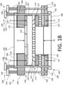
FIG. 1B is a side elevation view of a partial cross-section of a second assembly that includes the first assembly. -
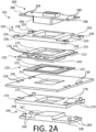
FIG. 2A is an exploded perspective view of a third assembly. -
FIG. 2B is a cross-sectional view of a portion of the third assembly. -
FIG. 2C is a perspective view of the third assembly in an assembled state. - All directional terms, such as "up," "down," "above," "below," "vertical," or "height" used in the following description refer only to the orientation of features as depicted in the figure being described. Such directional terms are not intended to suggest that any features of the devices described herein must exist in any particular orientation when constructed.
-
FIG. 1A shows afirst assembly 100 that includes aprocessor package 110 mounted to a printed circuit board ("PCB") 130.Processor package 110 includes aprocessor die 114 and apackage board 112.Package board 112 may be, for example, asubstrate supporting die 114. In other examples,package board 112 may be part of a power management system for a processor included inprocessor package 110, such as a capacitor board. In further examples,package board 112 may be a combination of multiple chips or boards, such as, for example, a substrate on top of a capacitor board.Processor package 110 can contain any type of processor, such as, for example, central processing unit ("CPU"), graphics processing unit ("GPU"), tensor processing unit ("TPU"), or any other type of processing unit which may generically be referred to as an "xPU."Processor package 110 could also be an application specific integrated circuit ("ASIC"). With respect to every reference to a microprocessor package in the present disclosure, the microprocessor package may optionally be an ASIC. -
First assembly 110 also contains asocket 120 that enablesprocessor package 110 to be mounted toPCB 130. In the illustrated arrangement,socket 120 includes asocket board 122 from which pins 124 extend in a direction away fromPCB 130.Pins 124 are pressed against corresponding pads on an underside ofpackage board 112 to establish an electronic connection therebetween, such as in a land grid array ("LGA") configuration.Socket board 122 is connected toPCB 130 bycontacts 125, which may be any type of electrical contact such as, for example, conductive pillars or balls of solder in a ball grid array ("BGA"). In various examples,contacts 125 may mechanically bondsocket board 122 toPCB 130 orcontacts 125 may merely establish an electrical connection betweensocket board 122 andPCB 130. In other arrangements,socket 120 may be a portion ofPCB 130 from which pins 124 extend instead of aseparate socket board 122. Regardless of whethersocket 120 is distinct fromPCB 130 or a part ofPCB 130,socket 120 may optionally lack vertical walls as shown in the illustrated arrangement. In other arrangements,socket 120 may include vertical walls around its periphery that create a concavity in whichprocessor package 110 can be received. - Though
pins 124 are part ofsocket 120 in the illustrated arrangement, in other arrangements pins 124 could instead be part ofprocessor package 110 and may, for example, extend from an underside ofpackage board 112 to press against corresponding pads onsocket 120 such as in a pin grid array ("PGA") configuration. In both LGA and PGA configurations,socket 120 andprocessor package 110 can be pressed ontopins 124 from opposite directions. -
Pins 124 are arranged around an area that is free ofpins 124 and defined bysocket aperture 121.Pins 124 are arranged in an array within which pins 124 are spaced apart from neighboringpins 124 by, in various examples, equal or approximately equal amounts, and the area that is free of pins is an area larger than the space betweenadjacent pins 124 within the array. The array ofpins 124 may have a rectangular outer perimeter with a length and width, and the area that is free of pins may be in the shape of a rectangle that extends across, in various examples, greater than or equal to 60%, 70%, 75%, 80%, 85%, or 90% of a length, width, or length and width of the rectangular outer perimeter of the array ofpins 124. The array ofpins 124 may extend along two, three, or four sides of the rectangular perimeter. In other examples, either or both of the array of pins and the area that is free of pins may be non-rectangular in shape, and in such other examples the area that is free of pins may be sized to have the same proportions relative to the array of pins as any of the possibilities described above with respect to examples wherein both the array of pins and the area free of pins have rectangular shapes. - In the illustrated example, the area that is free of pins is defined by a
socket aperture 121 that extends throughsocket board 122, though in other examples, the area that is free of pins may simply be a portion ofsocket 120 that is devoid ofpins 124 or pads for contactingpins 124. The presence ofpins 124 only along a perimeter ofsocket 120 contributes to even loading ofpins 124 by eliminating pins under the center ofpackage board 112, which would be subject to relatively little load ifpackage board 112 orPCB 130 became warped so that thepackage board 112 is farther fromsocket 120 at the center ofpackage board 112 than the edges ofpackage board 112. - High speed
electrical channels 116 fromdie 114 may run across a top surface ofpackage board 112. High speedelectrical channels 116 may be, for example, any lines configured to convey information at least at a certain minimum rate, such as, for example, 100 gigabits per second or greater or 200 gigabits per second or greater. In other examples, high speedelectrical channels 116 may be lines configured for establishing communication betweendie 114 and certain high-bandwidth connection types, such as, for example, Ethernet connections or optical communication connections or interfaces. Connections to high speedelectrical channel 116 may be made directly frompackage board 110 instead of elsewhere onPCB 130. Placing high-bandwidth channels 116 onpackage board 112 this way provides greater flexibility in configuring the shape ofsocket 120 by avoiding the need forsocket 120 to accommodate such high-bandwidth connections. Placingchannels 116 onpackage board 112 also avoids compromises to signal strength and quality that can occur when high bandwidth communications are routed throughsocket 120 and PCB, though some arrangements other than the illustrated arrangement route even high-bandwidth communications throughsocket 120 and alongPCB 130. Placingchannels 116 onpackage board 112 can also reduce the amount of interface area needed betweenprocessor package 110 andsocket 120. -
First assembly 100 also includes ablock 140 connected to an underside ofprocessor package 110.Block 140 may be any object, though in some examples, block 140 is part of a power management system forprocessor package 110. The power management system may be, for example, a voltage regulator or a vertical power module. Block 140 can be connected toprocessor package 110 in any manner, such as bycontacts 115. Likecontacts 125,contacts 115 may be any type of electrical contact such as, for example, conductive pillars or balls of solder in a BGA. In other examples, block 140 could be omitted altogether. - As shown in
FIG. 1B , asecond assembly 101 includesfirst assembly 100 and pressesprocessor package 110 andsocket 120 together 124 with clamping forces F2 and F3. Clamping forces F2, F3 are a force couple resulting from the compression offirst assembly 100 between alid 150 and a bolsterplate 174 ofsecond assembly 101.Load cells 190connect lid 150 andbase plate 160 together and drawlid 150 andbase plate 160 toward one another, thereby creating clamping forces F2, F3. - The illustrated example of
second assembly 101 also includes areinforcement plate 172 positioned on top ofpackage board 112.Reinforcement plate 172 acts to provide structural support to packageboard 112 and to narrow the area across which F2 is applied to packageboard 112.Reinforcement plate 172 includes areinforcement plate aperture 173 and has a footprint similar in shape and size to the area ofsocket 120 that includes pins 124. Force F2 as applied topackage board 112 throughreinforcement plate 172 is therefore laterally horizontally aligned with the support to the underside ofpackage board 112 provided bysocket 120. This horizontal alignment of force F2 withsocket 120 avoids creating a force moment onpackage board 112 and results in relatively even load on all pins 124. In arrangements other than the illustrated arrangement,reinforcement plate 172 could be shaped and sized differently or omitted altogether. -
Second assembly 101 also includes aheat sink 180 and abase plate 160 that create clamping forces F1 and F4. Clamping forces F1, F4 are a separate force couple from F2, F3. Clamping forces F1, F4 result fromload cells 190 pullingheat sink 180 andbase plate 160 together to loadheat sink 180 ontodie 114.Heat sink 180 extends withinlid aperture 151 to apply F1 to die 114, andbase plate 160 includes aplatform 167 extending into at least bolsterplate aperture 175 to apply F4 to an underside ofpackage board 112 in opposition to F1. In the illustrated example, force F4 is applied throughblock 140, but in other examples force F4 could be applied directly fromplatform 167 to packageboard 112. Platform is shown extending through bolsterplate aperture 175 and intoPCB aperture 131 whileblock 122 extends throughsocket aperture 121 intoPCB aperture 131, but the height ofplatform 167 and the thickness ofblock 140 can both vary, and the height ofplatform 167 can be adjusted or designed in any instance to extend as far into bolsterplate aperture 175,PCB aperture 131, andsocket aperture 120 as necessary to cooperate with any thickness ofblock 140 to apply an appropriate load to the underside ofprocessor package 110. The presence of ablock 140 on an underside ofprocessor package 110 and having enough thickness to extend intosocket aperture 121 andPCB aperture 131 can assist with aligningprocessor package 110 oversocket 120, reducing or eliminating the need for any vertical walls aroundsocket 120 to guideprocessor package 110. - Because
heat sink 180 andbase plate 160 are loaded bydifferent load cells 190 thanlid 150 and bolsterplate 174 and becauseheat sink 180 andbase plate 160 are movable relative tolid 150 and bolsterplate 174, the force couple of F1 and F4 is independent from the force couple of F2 and F3. The contact pressure betweenheat sink 180 and die 114 can therefore be adjusted independently of the compressive force applied topins 124. This ability to adjust the F2, F3 force couple independently of the F1, F4 force couple means loads betweenheat sink 180 and die 114 and loads onpins 124 can be optimized without concern for over- or under-loading the other. In other arrangements,heat sink 180 may be positionally fixed relative tolid 150 orbase plate 160 may be positionally fixed relative to or integrated with bolsterplate 174. In such other arrangements, the magnitude of forces F1, F4 can be adjusted independently of forces F2, F3 as long as either or bothheat sink 180 is vertically movable relative tolid 150 orbase plate 160 is vertically movable relative to bolsterplate 174. -
Load cells 190 of the illustrated example each include aspring 194 and ascrew 192 having ahead 196 against which spring 194 is trapped. Screw 192 of eachload cell 190 that includes aspring 194 trapped against the upper side oflid 150 is threadedly engaged with bolsterplate 174.Threadedly advancing screws 192 of thoseload cells 190 into bolsterplate 174 increases the pressure on the correspondingsprings 194 and thereby increases forces F2, F3. Similarly, screw 192 of eachload cell 190 that includes aspring 194 trapped against the upper side ofheat sink 180 is threadedly engaged withbase plate 160, so threadedly advancingscrews 192 of thoseload cells 190 intobase plate 160 increases forces F1, F4.Load cells 190 according to other examples can be any other device capable of pulling components ofsecond assembly 101 together. -
Heat sink 180 may include laterally extendingsink flanges 188 andbase plate 160 may include laterally extendingbase flanges 168 as shown. Sinkflanges 188 are thinner than a main body ofheat sink 180 that extends intolid aperture 151 to contact die 114. Similarly,base flanges 168 are thinner thanplatform 167 that extends into at least bolsterplate aperture 175 to load the underside ofprocessor package 110. The different thicknesses and lateral extend offlanges load cells 190 to engagebase plate 160 andheat sink 180 at locations laterally offset from the relatively narrow areas whereplatform 167 and the main body ofheat sink 180 transfer that load to other components in the form of forces F1, F4. -
FIGS. 2A and2C show anassembly 201, andFIG. 2B shows the components ofassembly 201 except for abase plate 260 in cross-section. Elements ofassembly 201 are alike to like numbered elements ofsecond assembly 101, meaning thatprocessor package 210 is alike toprocessor 110,heat sink 280 is alike toheat sink 180, and so on, except for specifically described or illustrated differences. Accordingly, certain elements ofassembly 201 enumerated in the figures may not be specifically mentioned in the present description. -
Heat sink 280 includeholes 289 throughsink flanges 288. Theholes 289 in the pair ofholes 289 in eachsink flange 288 are separated by a distance smaller than a distance betweentabs 258 oflid 250. Load cells 290 (not pictured inFIGS. 2A or2B ) applied to the top ofsink flanges 280 can therefore extend downward throughholes 289 and betweentabs 258 without contactinglid 250. However, in other examples without spaced aparttabs 258,lid 250 could be provided with additional holes to enable heat sink's 280load cells 290 to pass throughlid 250 without affectinglid 250. -
Tabs 258 also includeholes 259 so thatadditional load cells 290 can be placed atoptabs 258 to extend throughholes 259 andload lid 250.PCB 230 includesholes 239 extending therethrough to allow theload cells 290 atopheat sink 280 andlid 250 to pass throughPCB 230 without loadingPCB 230. - Bolster plate 270 includes internally threaded
standoffs 278 to accept threaded ends of screws of theload cells 290 applied to the top oflid 250. Theload cells 290 atoplid 250 can therefore extendpast reinforcement plate 272,processor package 210, andsocket 220 and throughPCB 230 to reach and engage bolsterplate 274. The lid's 250load cells 290 can thus drawlid 250 and bolsterplate 274 together, thereby creating a clamping force couple that compressesreinforcement plate 272,package board 212,socket 220, andPCB 230. Becausedie 214 is located inreinforcement plate aperture 273 and pins 224 surround asocket aperture 221 of equal or approximately equal dimensions toreinforcement plate aperture 273, this compression loadspins 274 betweensocket 220 and an underside ofpackage board 212 without compressingdie 214. - Bolster
plate 274 also includesholes 279 to enable theload cells 290 disposed throughholes 289 of heat sink to pass through bolsterplate 274 and reachbase plate 260 without loading bolsterplate 274. In other examples, instead of includingholes 279 bolsterplate 274 could include tabs, similar totabs 258, on whichstandoffs 278 could be located and between which the heat sink's 280load cells 290 could pass. -
Base plate 260 includes internally standoffs 269 aligned underholes 279 to accept threaded ends of screws of theload cells 290 applied to the top ofheat sink 280. Theload cells 290 atopheat sink 280 can therefore extendpast lid 250,reinforcement plate 272,processor package 210, andsocket 220 and throughPCB 230 and bolsterplate 274 to reach and engagebase plate 260. The heat sink's 280load cells 290 can thus drawheat sink 280 andbase plate 260 together, thereby creating a clamping force couple that presses abody 284 ofheat sink 280 into contact withdie 214. A total height ofbody 284,processor package 210, block 240, andplatform 267 exceeds a total height of the portions oflid 250,reinforcement plate 272,package board 212,socket 220,PCB 230, and bolsterplate 274 located betweenflanges load cells 290 to drawheat sink 280 andbase plate 260 together does not compress pins 224. - In the illustrated example,
standoffs standoffs overlying holes assembly 201 as they are stacked together. However, alternative arrangements could replacestandoffs plate 274 andbase plate 260. Still further variations could be made as appropriate in arrangements where loading devices other than screw andspring load cells 290 are used. - When
assembly 201 is stacked together as shown inFIG. 2C ,high speed channels 216 on the top side ofpackage board 212 are exposed and therefore accessible.High speed channels 216 can therefore be fitted with suitablehigh speed connectors 219, such as, for example, Ethernet ports, optical communication modules, or any other electronic connector. - Although the concept herein has been described with reference to particular examples, it is to be understood that these examples are merely illustrative of the principles and applications of the present concept. It is therefore to be understood that numerous modifications may be made to the illustrative examples and that other arrangements may be devised without departing from the spirit and scope of the present concept as defined by the appended claims.
Claims (15)
- An assembly, comprising:a printed circuit board ("PCB") including an aperture therethrough;an array of pins that extends around a perimeter of the aperture; anda processor package extending over the aperture and pressed against the array of pins by a first compressive force couple.
- The assembly of claim 1, comprising a socket that includes the array of pins and a socket board from which the array of pins extends.
- The assembly of claim 2, wherein the socket lacks walls at its periphery, and/orwherein the aperture is a PCB aperture and the socket board includes a socket aperture extending over the first aperture, and/orwherein the socket board is bonded to the PCB.
- The assembly of any one of the preceding claims, wherein the processor package includes a die compressed by a second force couple that is parallel to and independent of the first force couple, andcomprising optionally a base plate and a heat sink, wherein the second force couple is compression of the die between the base plate and the heat sink, andwherein force from the base plate is optionally transferred to the processor package by an object that extends into the aperture.
- The assembly of claim 4, comprising a bolster plate on an opposite side of the PCB from a lid, wherein the aperture is a PCB aperture, the bolster plate includes a bolster plate aperture aligned with the PCB aperture, and the lid includes a lid aperture aligned with the PCB aperture and into which the heat sink extends, and the first force couple is compression of the PCB and the processor package between the lid and the base plate.
- The assembly of any one of the preceding claims, comprising a block bonded to the processor package and extending into the aperture.
- The assembly of claim 6, wherein the block is a voltage regulator, and
wherein the block is optionally biased toward the processor package. - The assembly of any one of the preceding claims, wherein the processor package includes a die, a substrate, and a high speed electrical channel extending from the die across a surface of the board.
- An assembly, comprising:a PCB;an array of pins that extend from the PCB surrounding an area that is free of pins;a lid;a processor package clamped between the PCB and the lid, the processor package including a die, a package board, and a high speed electrical channel extending from the die and along the package board; anda high speed electrical connector mounted to the package board at an end of the high speed electrical channel.
- The assembly of claim 9, comprising a voltage regulator connected to an underside of the processor package extending into a PCB aperture in the PCB.
- The assembly of claim 10, wherein the array of pins extends around a perimeter of the PCB aperture.
- The assembly of any one of claims 9 to 11, comprising a heat sink extending through a lid aperture in the lid to contact the die and a base plate loaded against the heat sink to compress the die.
- The assembly of any one of claims 10 to 12, wherein load on the base plate is transferred to the processor package by an object disposed through the PCB aperture.
- The assembly of claim 13, comprising a bolster plate, wherein the processor package and PCB are clamped between the bolster plate and the lid.
- The assembly of claim 14, wherein the bolster plate includes a bolster plate aperture aligned with the PCB aperture and force from the base plate is transferred to the processor package through the bolster plate aperture and the PCB aperture.
Applications Claiming Priority (1)
| Application Number | Priority Date | Filing Date | Title |
|---|---|---|---|
| US17/722,860 US12308543B2 (en) | 2022-04-18 | 2022-04-18 | Structure for optimal XPU socket compression |
Publications (1)
| Publication Number | Publication Date |
|---|---|
| EP4266841A1 true EP4266841A1 (en) | 2023-10-25 |
Family
ID=84330406
Family Applications (1)
| Application Number | Title | Priority Date | Filing Date |
|---|---|---|---|
| EP22206410.7A Pending EP4266841A1 (en) | 2022-04-18 | 2022-11-09 | Improved structure for optimal xpu socket compression |
Country Status (3)
| Country | Link |
|---|---|
| US (1) | US12308543B2 (en) |
| EP (1) | EP4266841A1 (en) |
| CN (1) | CN115866889A (en) |
Families Citing this family (4)
| Publication number | Priority date | Publication date | Assignee | Title |
|---|---|---|---|---|
| US20220210950A1 (en) * | 2022-03-17 | 2022-06-30 | Intel Corporation | Multilayer back plate with molded ceramic layer |
| US12002795B2 (en) * | 2022-04-13 | 2024-06-04 | Google Llc | Pluggable CPU modules with vertical power |
| US12581591B2 (en) * | 2022-05-05 | 2026-03-17 | Nvidia Corp. | Circuit system and method of manufacturing a printed circuit board |
| US20240324108A1 (en) * | 2023-03-22 | 2024-09-26 | Intel Corporation | Architectures and methods that enable a reworkable heat management component |
Citations (6)
| Publication number | Priority date | Publication date | Assignee | Title |
|---|---|---|---|---|
| US20010032738A1 (en) * | 1999-07-15 | 2001-10-25 | Dibene Joseph Ted | Method and apparatus for providing power to a microprocessor with integrated thermal and EMI management |
| US20030214800A1 (en) * | 1999-07-15 | 2003-11-20 | Dibene Joseph Ted | System and method for processor power delivery and thermal management |
| US20050051889A1 (en) * | 2003-09-08 | 2005-03-10 | Wood Dustin P. | Integrated circuit packaging architecture |
| US20050248024A1 (en) * | 2004-05-06 | 2005-11-10 | Costello Brian P | Power delivery system for integrated circuits |
| WO2010096513A1 (en) * | 2009-02-18 | 2010-08-26 | Molex Incorporated | Electrical connector assembly with back plate |
| US20200245464A1 (en) * | 2019-01-30 | 2020-07-30 | Kyocera Corporation | Mounting structure |
Family Cites Families (51)
| Publication number | Priority date | Publication date | Assignee | Title |
|---|---|---|---|---|
| US4631820A (en) | 1984-08-23 | 1986-12-30 | Canon Kabushiki Kaisha | Mounting assembly and mounting method for an electronic component |
| US5127837A (en) * | 1989-06-09 | 1992-07-07 | Labinal Components And Systems, Inc. | Electrical connectors and IC chip tester embodying same |
| JPH047865A (en) | 1990-04-25 | 1992-01-13 | Hitachi Ltd | Lead frame and semiconductor integrated circuit device using the same |
| US5175613A (en) | 1991-01-18 | 1992-12-29 | Digital Equipment Corporation | Package for EMI, ESD, thermal, and mechanical shock protection of circuit chips |
| JP2931741B2 (en) | 1993-09-24 | 1999-08-09 | 株式会社東芝 | Semiconductor device |
| US5886408A (en) | 1994-09-08 | 1999-03-23 | Fujitsu Limited | Multi-chip semiconductor device |
| US5608262A (en) | 1995-02-24 | 1997-03-04 | Lucent Technologies Inc. | Packaging multi-chip modules without wire-bond interconnection |
| JPH08274214A (en) | 1995-03-30 | 1996-10-18 | Seiko Epson Corp | Semiconductor device |
| US5847929A (en) | 1996-06-28 | 1998-12-08 | International Business Machines Corporation | Attaching heat sinks directly to flip chips and ceramic chip carriers |
| KR100258350B1 (en) | 1997-05-13 | 2000-06-01 | 마이클 디. 오브라이언 | Super bga semiconductor package |
| JP3482850B2 (en) | 1997-12-08 | 2004-01-06 | セイコーエプソン株式会社 | Semiconductor device and its manufacturing method, circuit board, and electronic equipment |
| JP3087709B2 (en) | 1997-12-08 | 2000-09-11 | 日本電気株式会社 | Semiconductor device and manufacturing method thereof |
| DE19816794A1 (en) | 1998-04-16 | 1999-10-21 | Bosch Gmbh Robert | Printed circuit board system, for electronic combination instrument |
| WO2000004595A2 (en) | 1998-07-20 | 2000-01-27 | Intel Corporation | Land-side mounting of components to an integrated circuit package |
| US6154371A (en) | 1998-09-30 | 2000-11-28 | Cisco Technology, Inc. | Printed circuit board assembly and method |
| US20030156400A1 (en) | 1999-07-15 | 2003-08-21 | Dibene Joseph Ted | Method and apparatus for providing power to a microprocessor with intergrated thermal and EMI management |
| US6304450B1 (en) * | 1999-07-15 | 2001-10-16 | Incep Technologies, Inc. | Inter-circuit encapsulated packaging |
| JP3414342B2 (en) | 1999-11-25 | 2003-06-09 | 日本電気株式会社 | Mounting structure and mounting method of integrated circuit chip |
| EP1189282A4 (en) | 2000-03-21 | 2006-02-15 | Mitsubishi Electric Corp | SEMICONDUCTOR DEVICE, METHOD FOR PRODUCING ELECTRONIC DEVICE, ELECTRONIC DEVICE, AND PORTABLE INFORMATION TERMINAL |
| JP2001308258A (en) | 2000-04-26 | 2001-11-02 | Sony Corp | Semiconductor package and manufacturing method thereof |
| US7247932B1 (en) | 2000-05-19 | 2007-07-24 | Megica Corporation | Chip package with capacitor |
| JP4497683B2 (en) | 2000-09-11 | 2010-07-07 | ローム株式会社 | Integrated circuit device |
| JP2002314031A (en) | 2001-04-13 | 2002-10-25 | Fujitsu Ltd | Multi-chip module |
| DE10142655A1 (en) | 2001-08-31 | 2003-04-03 | Epcos Ag | component assembly |
| TW540988U (en) * | 2002-10-04 | 2003-07-01 | Hon Hai Prec Ind Co Ltd | A heat dissipating assembly |
| JP3093800U (en) | 2002-11-01 | 2003-05-16 | アルプス電気株式会社 | Electronic unit |
| JP2004288834A (en) | 2003-03-20 | 2004-10-14 | Fujitsu Ltd | Electronic component mounting method, mounting structure and package substrate |
| JPWO2004112450A1 (en) | 2003-06-12 | 2006-07-20 | 富士通株式会社 | Substrate mounting method and mounting structure |
| US7180165B2 (en) | 2003-09-05 | 2007-02-20 | Sanmina, Sci Corporation | Stackable electronic assembly |
| US20050127484A1 (en) | 2003-12-16 | 2005-06-16 | Texas Instruments Incorporated | Die extender for protecting an integrated circuit die on a flip chip package |
| DE202004002332U1 (en) | 2004-02-11 | 2004-04-22 | Siemens Ag | circuit board |
| US7085143B1 (en) | 2005-05-23 | 2006-08-01 | International Business Machines Corporation | In-module current source |
| JP4585416B2 (en) | 2005-09-22 | 2010-11-24 | 富士通株式会社 | Substrate warpage reduction structure and substrate warpage reduction method |
| US7476978B2 (en) | 2006-05-17 | 2009-01-13 | Infineon Technologies, Ag | Electronic component having a semiconductor power device |
| US7886431B2 (en) | 2006-06-06 | 2011-02-15 | Teraspeed Consulting Group Llc | Power distribution system for integrated circuits |
| US7773390B2 (en) | 2006-06-06 | 2010-08-10 | Teraspeed Consulting Group Llc | Power distribution system for integrated circuits |
| US20080081489A1 (en) * | 2006-09-29 | 2008-04-03 | Macgregor Mike G | Reliable land grid array socket loading device |
| JP4609435B2 (en) | 2007-01-30 | 2011-01-12 | パナソニック株式会社 | Component-embedded substrate, electronic device using the same, and manufacturing method used therefor |
| US7785114B2 (en) * | 2008-06-30 | 2010-08-31 | Intel Corporation | Modification of connections between a die package and a system board |
| US8837159B1 (en) | 2009-10-28 | 2014-09-16 | Amazon Technologies, Inc. | Low-profile circuit board assembly |
| JPWO2011121779A1 (en) | 2010-03-31 | 2013-07-04 | 富士通株式会社 | MULTI-CHIP MODULE, PRINTED WIRING BOARD UNIT, MULTI-CHIP MODULE MANUFACTURING METHOD, AND PRINTED WIRING BOARD UNIT MANUFACTURING METHOD |
| US8513798B2 (en) | 2010-09-09 | 2013-08-20 | Infineon Technologies Ag | Power semiconductor chip package |
| US8426258B2 (en) | 2010-10-12 | 2013-04-23 | Io Semiconductor, Inc. | Vertical semiconductor device with thinned substrate |
| US10312361B2 (en) | 2011-06-20 | 2019-06-04 | The Regents Of The University Of California | Trenched vertical power field-effect transistors with improved on-resistance and breakdown voltage |
| EP2627160A1 (en) | 2012-02-08 | 2013-08-14 | Harman Becker Automotive Systems GmbH | Circuit board system |
| JP6253885B2 (en) | 2013-01-07 | 2017-12-27 | ルネサスエレクトロニクス株式会社 | Vertical power MOSFET |
| WO2018182643A1 (en) | 2017-03-30 | 2018-10-04 | Intel Corporation | Three-dimensional decoupling integration within hole in motherboard |
| CN108710409B (en) * | 2017-07-05 | 2022-02-11 | 超聚变数字技术有限公司 | A processor fixing structure, component and computer equipment |
| EP3582259B1 (en) | 2018-06-11 | 2021-11-03 | AT & S Austria Technologie & Systemtechnik Aktiengesellschaft | Stepped component assembly accommodated within a stepped cavity in component carrier |
| CN109618538B (en) | 2018-12-29 | 2020-10-27 | 联想(北京)有限公司 | Accommodation equipment |
| CN113556916B (en) * | 2020-04-26 | 2023-02-28 | 台达电子企业管理(上海)有限公司 | Data processing apparatus |
-
2022
- 2022-04-18 US US17/722,860 patent/US12308543B2/en active Active
- 2022-11-09 EP EP22206410.7A patent/EP4266841A1/en active Pending
-
2023
- 2023-01-09 CN CN202310027449.6A patent/CN115866889A/en active Pending
Patent Citations (6)
| Publication number | Priority date | Publication date | Assignee | Title |
|---|---|---|---|---|
| US20010032738A1 (en) * | 1999-07-15 | 2001-10-25 | Dibene Joseph Ted | Method and apparatus for providing power to a microprocessor with integrated thermal and EMI management |
| US20030214800A1 (en) * | 1999-07-15 | 2003-11-20 | Dibene Joseph Ted | System and method for processor power delivery and thermal management |
| US20050051889A1 (en) * | 2003-09-08 | 2005-03-10 | Wood Dustin P. | Integrated circuit packaging architecture |
| US20050248024A1 (en) * | 2004-05-06 | 2005-11-10 | Costello Brian P | Power delivery system for integrated circuits |
| WO2010096513A1 (en) * | 2009-02-18 | 2010-08-26 | Molex Incorporated | Electrical connector assembly with back plate |
| US20200245464A1 (en) * | 2019-01-30 | 2020-07-30 | Kyocera Corporation | Mounting structure |
Also Published As
| Publication number | Publication date |
|---|---|
| US12308543B2 (en) | 2025-05-20 |
| CN115866889A (en) | 2023-03-28 |
| US20230335928A1 (en) | 2023-10-19 |
Similar Documents
| Publication | Publication Date | Title |
|---|---|---|
| US12308543B2 (en) | Structure for optimal XPU socket compression | |
| US10910748B2 (en) | Cable socket connector assembly for an electronic | |
| TWI848118B (en) | Electronic assembly including optical modules | |
| US6490161B1 (en) | Peripheral land grid array package with improved thermal performance | |
| TW202234970A (en) | Electronic assembly including a compression assembly for cable connector modules | |
| US20060202325A1 (en) | Method and structure to provide balanced mechanical loading of devices in compressively loaded environments | |
| US6750551B1 (en) | Direct BGA attachment without solder reflow | |
| US6477058B1 (en) | Integrated circuit device package including multiple stacked components | |
| US6354844B1 (en) | Land grid array alignment and engagement design | |
| TW202203516A (en) | Electronic assembly including cable modules | |
| US10541156B1 (en) | Multi integrated circuit chip carrier package | |
| US7298622B2 (en) | Modular heat sink assembly | |
| US8278745B2 (en) | Through board stacking of multiple LGA-connected components | |
| EP2575168A1 (en) | Electronic device | |
| JPH06338368A (en) | Electric-connector matching and operating assembly | |
| US20020123259A1 (en) | Electrical circuit connector with resilient pressure pads | |
| US20250081362A1 (en) | Electronic Apparatus | |
| US6010340A (en) | Solder column tip compliancy modification for use in a BGA socket connector | |
| US6731505B1 (en) | Integrated circuit mounting system with separate loading forces for socket and heat sink | |
| CN110071381B (en) | Cable receptacle connector assemblies for electronic enclosures | |
| CN1307745C (en) | Electric connector for printed circuit board | |
| US11128072B1 (en) | Electrical connector assembly having variable height contacts | |
| CN112055485B (en) | Electronic assembly with optical module | |
| HK40089883A (en) | Improved structure for optimal xpu socket compression | |
| US7950933B1 (en) | Electrical socket having contact terminals floatably arranged therein |
Legal Events
| Date | Code | Title | Description |
|---|---|---|---|
| STAA | Information on the status of an ep patent application or granted ep patent |
Free format text: STATUS: THE APPLICATION HAS BEEN PUBLISHED |
|
| PUAI | Public reference made under article 153(3) epc to a published international application that has entered the european phase |
Free format text: ORIGINAL CODE: 0009012 |
|
| AK | Designated contracting states |
Kind code of ref document: A1 Designated state(s): AL AT BE BG CH CY CZ DE DK EE ES FI FR GB GR HR HU IE IS IT LI LT LU LV MC ME MK MT NL NO PL PT RO RS SE SI SK SM TR |
|
| STAA | Information on the status of an ep patent application or granted ep patent |
Free format text: STATUS: REQUEST FOR EXAMINATION WAS MADE |
|
| 17P | Request for examination filed |
Effective date: 20240424 |
|
| RBV | Designated contracting states (corrected) |
Designated state(s): AL AT BE BG CH CY CZ DE DK EE ES FI FR GB GR HR HU IE IS IT LI LT LU LV MC ME MK MT NL NO PL PT RO RS SE SI SK SM TR |
|
| STAA | Information on the status of an ep patent application or granted ep patent |
Free format text: STATUS: EXAMINATION IS IN PROGRESS |
|
| 17Q | First examination report despatched |
Effective date: 20260109 |