EP4266484A1 - Effizienter wellenleiterübergang zwischen gehäuse und leiterplatte unter verwendung einer lötwand - Google Patents
Effizienter wellenleiterübergang zwischen gehäuse und leiterplatte unter verwendung einer lötwand Download PDFInfo
- Publication number
- EP4266484A1 EP4266484A1 EP23167569.5A EP23167569A EP4266484A1 EP 4266484 A1 EP4266484 A1 EP 4266484A1 EP 23167569 A EP23167569 A EP 23167569A EP 4266484 A1 EP4266484 A1 EP 4266484A1
- Authority
- EP
- European Patent Office
- Prior art keywords
- waveguide
- solder
- landing pads
- trace lines
- semiconductor device
- Prior art date
- Legal status (The legal status is an assumption and is not a legal conclusion. Google has not performed a legal analysis and makes no representation as to the accuracy of the status listed.)
- Withdrawn
Links
Images


Classifications
-
- H—ELECTRICITY
- H01—ELECTRIC ELEMENTS
- H01P—WAVEGUIDES; RESONATORS, LINES, OR OTHER DEVICES OF THE WAVEGUIDE TYPE
- H01P5/00—Coupling devices of the waveguide type
- H01P5/02—Coupling devices of the waveguide type with invariable factor of coupling
- H01P5/022—Transitions between lines of the same kind and shape, but with different dimensions
- H01P5/024—Transitions between lines of the same kind and shape, but with different dimensions between hollow waveguides
-
- H—ELECTRICITY
- H01—ELECTRIC ELEMENTS
- H01P—WAVEGUIDES; RESONATORS, LINES, OR OTHER DEVICES OF THE WAVEGUIDE TYPE
- H01P11/00—Apparatus or processes specially adapted for manufacturing waveguides or resonators, lines, or other devices of the waveguide type
- H01P11/001—Manufacturing waveguides or transmission lines of the waveguide type
- H01P11/002—Manufacturing hollow waveguides
-
- H—ELECTRICITY
- H01—ELECTRIC ELEMENTS
- H01P—WAVEGUIDES; RESONATORS, LINES, OR OTHER DEVICES OF THE WAVEGUIDE TYPE
- H01P3/00—Waveguides; Transmission lines of the waveguide type
- H01P3/12—Hollow waveguides
- H01P3/121—Hollow waveguides integrated in a substrate
-
- H—ELECTRICITY
- H05—ELECTRIC TECHNIQUES NOT OTHERWISE PROVIDED FOR
- H05K—PRINTED CIRCUITS; CASINGS OR CONSTRUCTIONAL DETAILS OF ELECTRIC APPARATUS; MANUFACTURE OF ASSEMBLAGES OF ELECTRICAL COMPONENTS
- H05K1/00—Printed circuits
- H05K1/02—Details
- H05K1/0213—Electrical arrangements not otherwise provided for
- H05K1/0237—High frequency adaptations
- H05K1/0243—Printed circuits associated with mounted high frequency components
-
- H—ELECTRICITY
- H05—ELECTRIC TECHNIQUES NOT OTHERWISE PROVIDED FOR
- H05K—PRINTED CIRCUITS; CASINGS OR CONSTRUCTIONAL DETAILS OF ELECTRIC APPARATUS; MANUFACTURE OF ASSEMBLAGES OF ELECTRICAL COMPONENTS
- H05K1/00—Printed circuits
- H05K1/02—Details
- H05K1/11—Printed elements for providing electric connections to or between printed circuits
- H05K1/111—Pads for surface mounting, e.g. lay-out
-
- H—ELECTRICITY
- H05—ELECTRIC TECHNIQUES NOT OTHERWISE PROVIDED FOR
- H05K—PRINTED CIRCUITS; CASINGS OR CONSTRUCTIONAL DETAILS OF ELECTRIC APPARATUS; MANUFACTURE OF ASSEMBLAGES OF ELECTRICAL COMPONENTS
- H05K3/00—Apparatus or processes for manufacturing printed circuits
- H05K3/10—Apparatus or processes for manufacturing printed circuits in which conductive material is applied to the insulating support in such a manner as to form the desired conductive pattern
-
- H—ELECTRICITY
- H05—ELECTRIC TECHNIQUES NOT OTHERWISE PROVIDED FOR
- H05K—PRINTED CIRCUITS; CASINGS OR CONSTRUCTIONAL DETAILS OF ELECTRIC APPARATUS; MANUFACTURE OF ASSEMBLAGES OF ELECTRICAL COMPONENTS
- H05K3/00—Apparatus or processes for manufacturing printed circuits
- H05K3/30—Assembling printed circuits with electric components, e.g. with resistors
- H05K3/32—Assembling printed circuits with electric components, e.g. with resistors electrically connecting electric components or wires to printed circuits
- H05K3/34—Assembling printed circuits with electric components, e.g. with resistors electrically connecting electric components or wires to printed circuits by soldering
- H05K3/341—Surface mounted components
- H05K3/3421—Leaded components
- H05K3/3426—Leaded components characterised by the leads
-
- H—ELECTRICITY
- H05—ELECTRIC TECHNIQUES NOT OTHERWISE PROVIDED FOR
- H05K—PRINTED CIRCUITS; CASINGS OR CONSTRUCTIONAL DETAILS OF ELECTRIC APPARATUS; MANUFACTURE OF ASSEMBLAGES OF ELECTRICAL COMPONENTS
- H05K3/00—Apparatus or processes for manufacturing printed circuits
- H05K3/40—Forming printed elements for providing electric connections to or between printed circuits
- H05K3/4007—Surface contacts, e.g. bumps
-
- H—ELECTRICITY
- H10—SEMICONDUCTOR DEVICES; ELECTRIC SOLID-STATE DEVICES NOT OTHERWISE PROVIDED FOR
- H10W—GENERIC PACKAGES, INTERCONNECTIONS, CONNECTORS OR OTHER CONSTRUCTIONAL DETAILS OF DEVICES COVERED BY CLASS H10
- H10W42/00—Arrangements for protection of devices
- H10W42/20—Arrangements for protection of devices protecting against electromagnetic or particle radiation, e.g. light, X-rays, gamma-rays or electrons
-
- H—ELECTRICITY
- H10—SEMICONDUCTOR DEVICES; ELECTRIC SOLID-STATE DEVICES NOT OTHERWISE PROVIDED FOR
- H10W—GENERIC PACKAGES, INTERCONNECTIONS, CONNECTORS OR OTHER CONSTRUCTIONAL DETAILS OF DEVICES COVERED BY CLASS H10
- H10W42/00—Arrangements for protection of devices
- H10W42/20—Arrangements for protection of devices protecting against electromagnetic or particle radiation, e.g. light, X-rays, gamma-rays or electrons
- H10W42/261—Arrangements for protection of devices protecting against electromagnetic or particle radiation, e.g. light, X-rays, gamma-rays or electrons characterised by their shapes or dispositions
- H10W42/263—Shielding bumps
-
- H—ELECTRICITY
- H10—SEMICONDUCTOR DEVICES; ELECTRIC SOLID-STATE DEVICES NOT OTHERWISE PROVIDED FOR
- H10W—GENERIC PACKAGES, INTERCONNECTIONS, CONNECTORS OR OTHER CONSTRUCTIONAL DETAILS OF DEVICES COVERED BY CLASS H10
- H10W42/00—Arrangements for protection of devices
- H10W42/20—Arrangements for protection of devices protecting against electromagnetic or particle radiation, e.g. light, X-rays, gamma-rays or electrons
- H10W42/261—Arrangements for protection of devices protecting against electromagnetic or particle radiation, e.g. light, X-rays, gamma-rays or electrons characterised by their shapes or dispositions
- H10W42/273—Arrangements for protection of devices protecting against electromagnetic or particle radiation, e.g. light, X-rays, gamma-rays or electrons characterised by their shapes or dispositions the arrangements being between laterally adjacent chips, e.g. walls between chips
-
- H—ELECTRICITY
- H10—SEMICONDUCTOR DEVICES; ELECTRIC SOLID-STATE DEVICES NOT OTHERWISE PROVIDED FOR
- H10W—GENERIC PACKAGES, INTERCONNECTIONS, CONNECTORS OR OTHER CONSTRUCTIONAL DETAILS OF DEVICES COVERED BY CLASS H10
- H10W44/00—Electrical arrangements for controlling or matching impedance
- H10W44/20—Electrical arrangements for controlling or matching impedance at high-frequency [HF] or radio frequency [RF]
-
- H—ELECTRICITY
- H10—SEMICONDUCTOR DEVICES; ELECTRIC SOLID-STATE DEVICES NOT OTHERWISE PROVIDED FOR
- H10W—GENERIC PACKAGES, INTERCONNECTIONS, CONNECTORS OR OTHER CONSTRUCTIONAL DETAILS OF DEVICES COVERED BY CLASS H10
- H10W70/00—Package substrates; Interposers; Redistribution layers [RDL]
- H10W70/01—Manufacture or treatment
- H10W70/05—Manufacture or treatment of insulating or insulated package substrates, or of interposers, or of redistribution layers
- H10W70/093—Connecting or disconnecting other interconnections thereto or therefrom, e.g. connecting bond wires or bumps
-
- H—ELECTRICITY
- H10—SEMICONDUCTOR DEVICES; ELECTRIC SOLID-STATE DEVICES NOT OTHERWISE PROVIDED FOR
- H10W—GENERIC PACKAGES, INTERCONNECTIONS, CONNECTORS OR OTHER CONSTRUCTIONAL DETAILS OF DEVICES COVERED BY CLASS H10
- H10W70/00—Package substrates; Interposers; Redistribution layers [RDL]
- H10W70/60—Insulating or insulated package substrates; Interposers; Redistribution layers
- H10W70/62—Insulating or insulated package substrates; Interposers; Redistribution layers characterised by their interconnections
- H10W70/65—Shapes or dispositions of interconnections
-
- H—ELECTRICITY
- H10—SEMICONDUCTOR DEVICES; ELECTRIC SOLID-STATE DEVICES NOT OTHERWISE PROVIDED FOR
- H10W—GENERIC PACKAGES, INTERCONNECTIONS, CONNECTORS OR OTHER CONSTRUCTIONAL DETAILS OF DEVICES COVERED BY CLASS H10
- H10W74/00—Encapsulations, e.g. protective coatings
- H10W74/01—Manufacture or treatment
- H10W74/012—Manufacture or treatment of encapsulations on active surfaces of flip-chip devices, e.g. forming underfills
-
- H—ELECTRICITY
- H10—SEMICONDUCTOR DEVICES; ELECTRIC SOLID-STATE DEVICES NOT OTHERWISE PROVIDED FOR
- H10W—GENERIC PACKAGES, INTERCONNECTIONS, CONNECTORS OR OTHER CONSTRUCTIONAL DETAILS OF DEVICES COVERED BY CLASS H10
- H10W74/00—Encapsulations, e.g. protective coatings
- H10W74/10—Encapsulations, e.g. protective coatings characterised by their shape or disposition
- H10W74/131—Encapsulations, e.g. protective coatings characterised by their shape or disposition the semiconductor body being only partially enclosed
-
- H—ELECTRICITY
- H10—SEMICONDUCTOR DEVICES; ELECTRIC SOLID-STATE DEVICES NOT OTHERWISE PROVIDED FOR
- H10W—GENERIC PACKAGES, INTERCONNECTIONS, CONNECTORS OR OTHER CONSTRUCTIONAL DETAILS OF DEVICES COVERED BY CLASS H10
- H10W74/00—Encapsulations, e.g. protective coatings
- H10W74/10—Encapsulations, e.g. protective coatings characterised by their shape or disposition
- H10W74/15—Encapsulations, e.g. protective coatings characterised by their shape or disposition on active surfaces of flip-chip devices, e.g. underfills
-
- H—ELECTRICITY
- H05—ELECTRIC TECHNIQUES NOT OTHERWISE PROVIDED FOR
- H05K—PRINTED CIRCUITS; CASINGS OR CONSTRUCTIONAL DETAILS OF ELECTRIC APPARATUS; MANUFACTURE OF ASSEMBLAGES OF ELECTRICAL COMPONENTS
- H05K1/00—Printed circuits
- H05K1/02—Details
- H05K1/0213—Electrical arrangements not otherwise provided for
- H05K1/0216—Reduction of cross-talk, noise or electromagnetic interference
- H05K1/0218—Reduction of cross-talk, noise or electromagnetic interference by printed shielding conductors, ground planes or power plane
-
- H—ELECTRICITY
- H05—ELECTRIC TECHNIQUES NOT OTHERWISE PROVIDED FOR
- H05K—PRINTED CIRCUITS; CASINGS OR CONSTRUCTIONAL DETAILS OF ELECTRIC APPARATUS; MANUFACTURE OF ASSEMBLAGES OF ELECTRICAL COMPONENTS
- H05K2201/00—Indexing scheme relating to printed circuits covered by H05K1/00
- H05K2201/03—Conductive materials
- H05K2201/0332—Structure of the conductor
- H05K2201/0364—Conductor shape
- H05K2201/037—Hollow conductors, i.e. conductors partially or completely surrounding a void, e.g. hollow waveguides
-
- H—ELECTRICITY
- H05—ELECTRIC TECHNIQUES NOT OTHERWISE PROVIDED FOR
- H05K—PRINTED CIRCUITS; CASINGS OR CONSTRUCTIONAL DETAILS OF ELECTRIC APPARATUS; MANUFACTURE OF ASSEMBLAGES OF ELECTRICAL COMPONENTS
- H05K2201/00—Indexing scheme relating to printed circuits covered by H05K1/00
- H05K2201/10—Details of components or other objects attached to or integrated in a printed circuit board
- H05K2201/10613—Details of electrical connections of non-printed components, e.g. special leads
- H05K2201/10621—Components characterised by their electrical contacts
- H05K2201/10734—Ball grid array [BGA]; Bump grid array
-
- H—ELECTRICITY
- H05—ELECTRIC TECHNIQUES NOT OTHERWISE PROVIDED FOR
- H05K—PRINTED CIRCUITS; CASINGS OR CONSTRUCTIONAL DETAILS OF ELECTRIC APPARATUS; MANUFACTURE OF ASSEMBLAGES OF ELECTRICAL COMPONENTS
- H05K2201/00—Indexing scheme relating to printed circuits covered by H05K1/00
- H05K2201/10—Details of components or other objects attached to or integrated in a printed circuit board
- H05K2201/10613—Details of electrical connections of non-printed components, e.g. special leads
- H05K2201/10954—Other details of electrical connections
- H05K2201/10977—Encapsulated connections
-
- H—ELECTRICITY
- H05—ELECTRIC TECHNIQUES NOT OTHERWISE PROVIDED FOR
- H05K—PRINTED CIRCUITS; CASINGS OR CONSTRUCTIONAL DETAILS OF ELECTRIC APPARATUS; MANUFACTURE OF ASSEMBLAGES OF ELECTRICAL COMPONENTS
- H05K3/00—Apparatus or processes for manufacturing printed circuits
- H05K3/30—Assembling printed circuits with electric components, e.g. with resistors
- H05K3/32—Assembling printed circuits with electric components, e.g. with resistors electrically connecting electric components or wires to printed circuits
- H05K3/34—Assembling printed circuits with electric components, e.g. with resistors electrically connecting electric components or wires to printed circuits by soldering
- H05K3/341—Surface mounted components
- H05K3/3431—Leadless components
- H05K3/3436—Leadless components having an array of bottom contacts, e.g. pad grid array or ball grid array components
-
- H—ELECTRICITY
- H10—SEMICONDUCTOR DEVICES; ELECTRIC SOLID-STATE DEVICES NOT OTHERWISE PROVIDED FOR
- H10W—GENERIC PACKAGES, INTERCONNECTIONS, CONNECTORS OR OTHER CONSTRUCTIONAL DETAILS OF DEVICES COVERED BY CLASS H10
- H10W44/00—Electrical arrangements for controlling or matching impedance
- H10W44/20—Electrical arrangements for controlling or matching impedance at high-frequency [HF] or radio frequency [RF]
- H10W44/203—Electrical connections
- H10W44/216—Waveguides, e.g. strip lines
-
- H—ELECTRICITY
- H10—SEMICONDUCTOR DEVICES; ELECTRIC SOLID-STATE DEVICES NOT OTHERWISE PROVIDED FOR
- H10W—GENERIC PACKAGES, INTERCONNECTIONS, CONNECTORS OR OTHER CONSTRUCTIONAL DETAILS OF DEVICES COVERED BY CLASS H10
- H10W44/00—Electrical arrangements for controlling or matching impedance
- H10W44/20—Electrical arrangements for controlling or matching impedance at high-frequency [HF] or radio frequency [RF]
- H10W44/241—Electrical arrangements for controlling or matching impedance at high-frequency [HF] or radio frequency [RF] for passive devices or passive elements
- H10W44/248—Electrical arrangements for controlling or matching impedance at high-frequency [HF] or radio frequency [RF] for passive devices or passive elements for antennas
-
- H—ELECTRICITY
- H10—SEMICONDUCTOR DEVICES; ELECTRIC SOLID-STATE DEVICES NOT OTHERWISE PROVIDED FOR
- H10W—GENERIC PACKAGES, INTERCONNECTIONS, CONNECTORS OR OTHER CONSTRUCTIONAL DETAILS OF DEVICES COVERED BY CLASS H10
- H10W74/00—Encapsulations, e.g. protective coatings
- H10W74/10—Encapsulations, e.g. protective coatings characterised by their shape or disposition
- H10W74/131—Encapsulations, e.g. protective coatings characterised by their shape or disposition the semiconductor body being only partially enclosed
- H10W74/142—Encapsulations, e.g. protective coatings characterised by their shape or disposition the semiconductor body being only partially enclosed the encapsulations exposing the passive side of the semiconductor body
-
- H—ELECTRICITY
- H10—SEMICONDUCTOR DEVICES; ELECTRIC SOLID-STATE DEVICES NOT OTHERWISE PROVIDED FOR
- H10W—GENERIC PACKAGES, INTERCONNECTIONS, CONNECTORS OR OTHER CONSTRUCTIONAL DETAILS OF DEVICES COVERED BY CLASS H10
- H10W90/00—Package configurations
- H10W90/701—Package configurations characterised by the relative positions of pads or connectors relative to package parts
- H10W90/721—Package configurations characterised by the relative positions of pads or connectors relative to package parts of bump connectors
- H10W90/724—Package configurations characterised by the relative positions of pads or connectors relative to package parts of bump connectors between a chip and a stacked insulating package substrate, interposer or RDL
Definitions
- the present invention is directed in general to the field of integrated circuit devices and packages.
- the present invention relates to electronic component packaging and method of manufacturing for an integrated circuit package having a radio frequency device.
- the integrated circuit package may be mounted to a printed circuit board (PCB) which can have other components and devices mounted on the PCB, such as a waveguide launcher or antenna elements.
- PCB printed circuit board
- the PCB may include waveguide apertures formed in the PCB substrate to promote radio frequency coupling between the integrated circuit package and any PCB components or devices.
- An integrated circuit package assembly, apparatus, and fabrication method are described for attaching an integrated circuit package to one or more external waveguide structures using a printed circuit board (PCB) substrate having a patterned array of solder bridge trace lines and landing pads on a first surface of the PCB substrate.
- the solder bridge trace lines are positioned to surround the periphery of waveguide openings formed in the PCB substrate.
- a solder mask may be applied to the first surface of the PCB substrate which exposes the patterned array of solder bridge trace lines and landing pads, and an integrated circuit package having a ball grid array (BGA) is attached to the PCB substrate with the BGA solder ball conductors aligned for contact with the patterned landing pads.
- BGA ball grid array
- the BGA solder ball conductors which are positioned at the periphery of waveguide openings flow together along the solder bridge trace lines to form a closed solder wall between PCB substrate and integrated circuit package, thereby forming waveguide shielding walls around the waveguide openings which reduce radio frequency (RF) signal leakage between adjacent transmit or receive channels.
- RF radio frequency
- the waveguide shielding walls prevent underfill encapsulant materials from intruding into the waveguide openings of the PCB substrate, thereby enhancing reliability of the solder connection and extending the product lifetime.
- integrated circuit packages which include integrated radio frequency (RF) circuits (e.g., receiver, transmitter, and/or transceiver circuits) are typically connected to a patterned array of landing pads on a PCB substrate using conductive bump structures.
- RF radio frequency
- the PCB substrates typically include RF waveguides formed in the PCB substrate with one or more waveguide holes or apertures formed in alignment with the RF circuits to extend through the PCB substrate.
- each waveguide hole or aperture will be surrounded by a plurality of separate conductive bump structures in which openings or gaps between the conductive bump structures provide an electrically and physically "open” structure which reduces signal efficiency and channel isolation since the RF signals being transmitted through the RF waveguides can "leak" through the openings or gaps.
- the openings or gaps between the conductive bump structures prevent the ability to use underfill materials to adhesively bond surface mount integrated circuit packages to the PCB substrate since the underfill material can penetrate through the openings or gaps to intrude into RF waveguides.
- FIG. 1 depicts a plan view 10 of a printed circuit board (PCB) substrate 11 in which waveguide apertures or openings 12, 32 are formed.
- PCB printed circuit board
- an array of patterned conductive landing pads 13, 33 and shield wall landing pads and trace lines 14/15, 34/35 are formed.
- the layout of the patterned conductive landing pads 13, 33 is arranged on the top surface of the PCB substrate 11 to provide electrical connection to PCB conductor elements or vias (not shown) formed in the PCB substrate 11, thereby allowing subsequently-formed conductive bump structures (e.g., BGA solder balls) from an integrated circuit package to make electrical contact to the PCB conductor elements/vias.
- conductive bump structures e.g., BGA solder balls
- the layout of the patterned conductive shield wall landing pads 14, 34 and trace lines 15, 35 is arranged to provide electrical connection to PCB conductor elements/vias (not shown) formed in the PCB substrate 11, and to also encircle and surround, respectively, the waveguide apertures or openings 12, 32.
- a plurality of conductive contact pads or layers 14A-C are formed on the top surface of the PCB substrate 11 to surround each of the waveguide apertures or openings 12A-C.
- conductive trace layers 15A-C are formed on the top surface of the PCB substrate 11 to connect the conductive contact pads or layers 14A-C together, thereby providing a wettable surface between the conductive contact pads or layers 14A-C at the periphery of the waveguide apertures or openings 12.
- each waveguide opening (e.g., 12A) has a separate set of patterned conductive shield wall landing pads (e.g., 14A) connected together by conductive trace lines (e.g., 15A).
- conductive trace lines e.g., 15A
- the patterned conductive shield wall landing pads 14A-C and trace lines 15A-C are connected to a predetermined reference or supply voltage, such as ground, when in operational mode to provide the waveguide shielding benefits described more fully hereinbelow.
- the patterned conductive shield wall landing pads 34 are formed on the top surface of the PCB substrate 11 to surround the waveguide apertures or openings 32A-D, but with only a single row of landing pads 34 positioned between adjacent waveguide openings.
- patterned conductive shield wall trace lines 35 are formed on the top surface of the PCB substrate 11 to connect the conductive contact pads or layers 34 together, thereby providing a wettable surface between the conductive contact pads or layers 34 at the periphery of the waveguide apertures or openings 32.
- a single, contiguous set of patterned conductive shield wall landing pads 34 and trace lines 35 are formed to surround the waveguide openings (e.g., 32A-D).
- the gray shading of the patterned conductive shield wall landing pads 34 and trace lines 35 indicates they are connected to a predetermined reference or supply voltage, such as ground, when in operational mode to provide the waveguide shielding benefits described more fully hereinbelow.
- FIG. 2A shows a cross-sectional view (through line Fig. 2A of Figure 1 ) of the PCB substrate 11 at a first stage of a package fabrication process in accordance with selected first embodiments of the present disclosure.
- the PCB substrate 11 may be initially formed with one or more dielectric material layers and may include patterned conductive via and/or lines to provide predetermined electrical connections to patterned landing pads 13, 14 formed on a first or top surface of the PCB substrate.
- waveguide openings or apertures 12A-C may be formed in the PCB substrate 11 at predetermined locations.
- a first set of RF waveguides may be positioned in the PCB substrate 11 for alignment with RF circuits formed in integrated circuit packages that are subsequently mounted or attached to the PCB substrate 11.
- a conductive pattern of landing pads 13, 14 and patterned trace lines 15 are formed for purposes of electrically and physically connecting to the (subsequently formed) solder balls of a (subsequently attached) integrated circuit package.
- a first set of contact pads or layers 13 may be formed on the top surface of the PCB substrate 11 and electrically connected to one or more conductive vias (not shown) formed in the PCB substrate 11.
- a second set of patterned contact pads 14A-C and trace lines 15A-C are formed on the top surface of the PCB substrate 11 and positioned peripherally to the waveguide apertures or openings 12A-C.
- any suitable fabrication sequence may be used to form the conductive pattern of landing pads 13, 14 and patterned trace lines 15.
- one or more conductive layers may be deposited (e.g., electroplated) on the PCB substrate 11, and then patterned and etched using photolithography processes to selectively etch the deposited conductive layer(s) to form the conductive pattern of landing pads 13, 14 and patterned trace lines 15.
- the patterning and etching of the deposited conductive layer(s) may also form metallized sidewall plating layers (not shown) which extend down interior sidewalls of the waveguide openings or apertures 12A-C.
- the conductive landing pads 13, 14 and patterned trace lines 15 may be formed from any reflowable conductive material, including but not limited to a conductive metal (e.g., copper) or metal alloy, conductive or conductor-filled elastomer, or any other conductive material used for electrical connections known to those skilled in the art.
- FIG. 2B there is depicted a cross-sectional side view of the PCB substrate 11 with a patterned solder mask 16 at a stage of a package fabrication process after Figure 2A .
- the patterned solder mask 16 may be formed by applying a solder masking layer to cover the first surface of the PCB substrate 11, and then using photolithography processes to selectively expose and develop the solder masking layer so that solder mask openings are formed to expose the conductive pattern of landing pads 13, 14 and patterned trace lines 15.
- the ball grid array package 20 may be a radio frequency integrated circuit (RFIC) package which includes integrated receive RX and/or transmit TX circuits 23-25, and which includes other circuits which are connected through conductive traces (not shown) to the landing pads 21 and BGA solder ball conductors 22.
- RFIC radio frequency integrated circuit
- the ball grid array package 20 may include a solder mask layer (not shown) that is affixed to bottom of the package and that has a plurality of solder ball openings in which the solder ball conductors 22 are affixed in electrical contact with an associated landing pad 21.
- the RX and/or transmit TX circuits 23-25 are aligned with the waveguide apertures or openings 12A-C to transmit and/or receive RF signals through the PCB substrate 11.
- the solder ball conductors 22 are aligned with the openings in the patterned solder mask 16 to make electrical contact with the conductive pattern of landing pads 13, 14.
- FIG. 2D there is depicted a cross-sectional side view of the ball grid array package 20 mounted to the PCB substrate 11 after a heat reflow process has been applied at a stage of a package fabrication process after Figure 2C .
- the heat reflow process joins selected solder balls 22 that are positioned adjacent to the waveguide apertures or openings 12A-C, thereby forming the waveguide shielding walls 27-29 as a closed solder wall between the PCB substrate 11 and RFIC package 20.
- the heat reflow process will reflow all of the solder balls 22, but the solder balls 22 attached to the landing pads 13 are depicted with "round" shapes to indicate that they have not joined with other solder balls, while the "square" shape of the solder balls 27-29 attached to the landing pads 14 indicate that they have been reflowed and joined with other solder balls to form the waveguide shielding walls 27-29.
- the thermal heat treatment step is applied with a controlled duration and temperature to maintain separation of the individual solder balls formed on the landing pads 13, and to allow the individual solder balls 22 formed on the landing pads 14 to reflow and join together to form the waveguide shielding walls 27-29.
- the reflow process is promoted by choosing the correct time and temperature for the thermal heat treatment.
- the reflow process is promoted by virtue of the exposed conductive trace lines 15 which are positioned to connect the landing pads 14 for the reflow solder balls 22.
- the reflow process is promoted by virtue of the patterned solder mask 16 having no solder mask covering an exposed conductive trace line 15 between the reflow solder balls 22.
- the reflow process may be promoted by using a stencil during application of the solder paste which is adapted to print additional solder paste on the conductive trace lines 15 to facilitate the joining of the solder balls on the solder lands 14 and the exposed trace lines 15 connecting them.
- FIG. 2E there is depicted a plan view (through line Fig. 2E shown in Figure 2D ) of the mounted ball grid array package 20 and the PCB substrate 11 to illustrate how the reflowed solder balls 22 formed on the landing pads 14 join together in the defined openings of the solder mask 16 to form the waveguide shielding walls 27-29 around the waveguide apertures or openings 12A-C.
- solder balls 22 By joining the solder balls 22 together with a thermal reflow process to form the closed solder waveguide walls 27-29 between PCB substrate 11 and RFIC package 20, signal leakage between channels formed with the adjacent receive RX and/or transmit TX circuits 23-25 is prevented by the shielding function provided by the fully closed waveguide walls 27-29, thereby improving signal efficiency and channel isolation.
- FIG. 2F there is depicted a cross-sectional side view of the mounted ball grid array package 20 and the PCB substrate 11 after forming an underfill layer 30 has been formed at a stage of a package fabrication process after Figure 2D .
- the underfill layer 30 may be injected between the PCB substrate 11 and the ball grid array package 20 from one or more external injection sites to help bond the ball grid array package 20 to the PCB substrate 11 and to reinforce the solder bumps, thereby improving the reliability of the packaged assembly.
- a liquid underfill dispense technique may be used to apply the underfill at the edges of the ball grid array package 20 and the PCB substrate 11, and capillary action wicks the fluid into the interior regions.
- the entire die surface is coated with the underfill except for the areas surrounded and protected by the closed solder waveguide walls 27-29.
- the solder waveguide walls 27-29 prevent underfill material 30 from polluting the waveguide transition area between the ball grid array package 20 and the PCB substrate 11, but still allow the device reliability to be improved by forming the underfill layer 30 in other areas of the package assembly, including any openings or spaces between the solder waveguide walls 27-29.
- the use of underfill layer 30 and/or edge bonding will allow a heatsink to be mounted to the package without creating excessive stress on the solder joint and/or the potential creep of the solder joints under pressure. In particular, higher forces can be used in cases where the underfill layer 30 is formed. However, it will be appreciated that, even without an underfill layer 30, a heatsink can be contacted to the package.
- the specific structure and arrangement of the solder waveguide walls can be adjusted by controlling the placement of the shield wall landing pads and trace lines.
- Figure 3A shows a cross-sectional view (through line Fig. 3A of Figure 1 ) of the PCB substrate 11 at a first stage of a package fabrication process in accordance with selected second embodiments of the present disclosure.
- the PCB substrate 11 includes a plurality of waveguide openings or apertures 32A-D which define a second set of RF waveguides in the PCB substrate 11 for alignment with RF circuits formed in integrated circuit packages that are subsequently mounted or attached to the PCB substrate 11.
- a conductive pattern of landing pads 33, 34 and patterned trace lines 35 are formed for electrically and physically connecting to the (subsequently formed) solder balls of a (subsequently attached) integrated circuit package.
- a first set of contact pads or layers 33 may be formed on the top surface of the PCB substrate 11 and electrically connected to one or more conductive vias (not shown) formed in the PCB substrate 11 using any suitable fabrication sequence.
- a second set of patterned contact pads 34 and trace lines 35 are formed on the top surface of the PCB substrate 11 and positioned peripherally to the waveguide apertures or openings 32A-D.
- one or more conductive layers may be deposited on the PCB substrate 11, and then patterned and etched using photolithography processes to selectively etch the deposited conductive layer(s) to form the conductive pattern of landing pads 33, 34 and patterned trace lines 35.
- the patterning and etching of the deposited conductive layer(s) may also form metallized sidewall plating layers (not shown) which extend down interior sidewalls of the waveguide openings or apertures 32A-D.
- the conductive landing pads 33, 34 and patterned trace lines 35 may be formed from any conductive material used for electrical connections known to those skilled in the art.
- FIG. 3B there is depicted a cross-sectional side view of the PCB substrate 11 with a patterned solder mask 36 at a stage of a package fabrication process after Figure 3A .
- the patterned solder mask 36 may be formed using any suitable fabrication process to cover the first surface of the PCB substrate 11 with a solder mask layer which is then photolithographically processed to selectively expose and develop the solder masking layer to form solder mask openings that expose the conductive pattern of landing pads 33, 34 and patterned trace lines 35.
- the ball grid array package 40 may be a radio frequency integrated circuit (RFIC) package which includes integrated receive RX and/or transmit TX circuits 43A-D which are connected through conductive traces (not shown) to the landing pads 41 and affixed BGA solder ball conductors 42.
- RFIC radio frequency integrated circuit
- the RX and/or transmit TX circuits 43A-D are aligned with the waveguide apertures or openings 32A-D to transmit and/or receive RF signals through the PCB substrate 11.
- the solder ball conductors 42 are aligned with the openings in the patterned solder mask 36 to make electrical contact with the conductive pattern of landing pads 33, 34.
- FIG. 3D there is depicted a cross-sectional side view of the ball grid array package 40 mounted to the PCB substrate 11 after a heat reflow process has been applied at a stage of a package fabrication process after Figure 3C .
- the heat reflow process joins selected solder balls 42 that are positioned adjacent to the waveguide apertures or openings 32A-D, thereby forming the waveguide shielding walls 45 as a single, continuous, closed solder wall between the PCB substrate 11 and RFIC package 40.
- the heat reflow process will reflow all of the solder balls 42, but the solder balls 42 attached to the landing pads 34 are depicted with "square" shapes to indicate that they have been reflowed and joined with other solder balls to form the waveguide shielding walls 45.
- the thermal heat treatment step is applied with a controlled duration and temperature to maintain separation of the individual solder balls formed on the landing pads 33, and to allow the individual solder balls 42 formed on the landing pads 34 to reflow and join together to form the waveguide shielding walls 45.
- the reflow process is promoted by virtue of the exposed conductive trace lines 35 which are not covered by the solder mask 45 and which are positioned to connect the landing pads 34 for the reflow solder balls 42.
- the reflow process may be promoted by using a stencil during application of the solder paste which is adapted to print additional solder paste on the conductive trace lines 35 to facilitate the joining of the solder balls on the solder lands 34 and the exposed trace lines 35 connecting them.
- FIG. 3E there is depicted a plan view (through line Fig. 3E shown in Figure 3D ) of the mounted ball grid array package 40 and the PCB substrate 11 to illustrate how the reflowed solder balls 42 formed on the landing pads 34 join together in the defined openings of the solder mask 36 to form the waveguide shielding walls 45 around the waveguide apertures or openings 32A-D.
- the solder balls 42 By joining the solder balls 42 together with a thermal reflow process to form the closed solder waveguide walls 45 between PCB substrate 11 and RFIC package 40, signal leakage between channels formed with the adjacent receive RX and/or transmit TX circuits 43A-D is prevented by the shielding function provided by the fully closed waveguide walls 45, thereby improving signal efficiency and channel isolation.
- the closed solder waveguide walls 45 with only a single row of solder balls 42 positioned between adjacent waveguide openings, a more compact arrangement of RF waveguides may be formed with protective shielding.
- FIG. 3F there is depicted a cross-sectional side view of the mounted ball grid array package 40 and the PCB substrate 11 after forming an underfill layer 37 at a stage of a package fabrication process after Figure 3D .
- the underfill layer 37 may be injected between the PCB substrate 11 and the ball grid array package 40 from one or more external injection sites to help bond the ball grid array package 40 to the PCB substrate 11 and to reinforce the solder bumps, thereby improving the reliability of the packaged assembly while also preventing underfill material 37 from polluting the waveguide transition area between the ball grid array package 40 and the PCB substrate 11.
- the use of underfill layer 37 and/or edge bonding will allow a heatsink to be mounted to the package without creating excessive stress on the solder joint and/or the potential creep of the solder joints under pressure.
- the use of patterned openings in the solder mask (e.g., 36) to position the solder balls (e.g., 42) at the periphery of the waveguide openings (e.g., 32) can result in the waveguide shielding walls (e.g., 45) being laterally displaced or non-aligned with the waveguide aperture sidewalls.
- Such discontinuities in the RF waveguide sidewalls can interfere with RF signal transmission or reception.
- the specific structure and arrangement of the solder waveguide walls can be adjusted by controlling the placement of the reflow solder balls, landing pads, and trace lines so that the waveguide shielding walls are aligned with the waveguide openings.
- FIG. 4A shows a cross-sectional view of a PCB substrate 51 at a first stage of a package fabrication process in accordance with selected third embodiments of the present disclosure.
- the PCB substrate 51 includes a plurality of waveguide openings or apertures 52A-C which define a set of RF waveguides in the PCB substrate 51 for alignment with RF circuits formed in integrated circuit packages that are subsequently mounted or attached to the PCB substrate 51.
- a conductive pattern of landing pads 53 and trace lines 54 are formed for electrically and physically connecting to the (subsequently formed) solder balls of a (subsequently attached) integrated circuit package.
- a first set of contact pads or layers 53 may be formed on the top surface of the PCB substrate 51 and electrically connected to one or more conductive vias (not shown) formed in the PCB substrate 51 using any suitable fabrication sequence.
- a second set of patterned contact pads and trace lines 54 are formed on the top and bottom surfaces of the PCB substrate 51 and on the sidewalls of the waveguide openings 52A-C to cover the peripheral edges of the waveguide openings 52A-C.
- one or more conductive layers may be deposited (e.g., electroplated) on the PCB substrate 51, and then patterned and etched using photolithography processes to selectively etch the deposited conductive layer(s) to form the conductive pattern of landing pads 53 and the sidewall plating layer of the patterned trace lines/pads 54.
- the conductive landing pads 53 and patterned trace lines/pads 54 may be formed from any conductive material used for electrical connections known to those skilled in the art.
- FIG. 4B there is depicted a cross-sectional side view of the PCB substrate 51 with a patterned solder mask 55 at a stage of a package fabrication process after Figure 4A .
- the patterned solder mask 55 may be formed using any suitable fabrication process to cover the first surface of the PCB substrate 51 with a solder mask layer which is then photolithographically processed to selectively expose and develop the solder masking layer to form solder mask openings that expose the conductive landing pads 53 and patterned trace lines/pads 54.
- the ball grid array package 60 may be an RFIC package which includes integrated receive RX and/or transmit TX circuits 63A-C which are connected through conductive traces (not shown) to the landing pads 61 and affixed BGA solder ball conductors 62. As formed, the RX and/or transmit TX circuits 63A-C are aligned with the waveguide apertures or openings 52A-C to transmit and/or receive RF signals through the PCB substrate 51.
- solder ball conductors 62 are aligned with the openings in the patterned solder mask 55 to make electrical contact with the conductive landing pads 53 and patterned trace lines/pads 54. In this way, the solder ball conductors 62 nearest the waveguide openings 52A-C may be placed in close proximity to the waveguide opening sidewalls.
- FIG. 4D there is depicted a cross-sectional side view of the ball grid array package 60 mounted to the PCB substrate 51 after a heat reflow process has been applied at a stage of a package fabrication process after Figure 4C .
- the heat reflow process joins selected solder balls 62 that are positioned adjacent to the waveguide apertures or openings 52A-C, thereby forming separate waveguide shielding walls 64, 65, 66 which each form a closed solder wall between the PCB substrate 51 and RFIC package 60.
- the heat reflow process will reflow all of the solder balls 62, but the solder balls 62 attached to the landing pads 53 are depicted with "round" shapes to indicate that they have not joined with other solder balls, while the "square" shape of the solder balls 64-66 attached to the landing pads 54 indicate that they have been reflowed and joined with other solder balls to form the waveguide shielding walls 64-65.
- the thermal heat treatment step is applied with a controlled duration and temperature to maintain separation of the individual solder balls 62 formed on the landing pads 53, and to allow the individual solder balls 62 formed on the patterned trace lines/ pads 54 to reflow and join together to form the waveguide shielding walls 64-66.
- the reflow process is promoted by virtue of the exposed conductive trace lines 54 which are not covered by the solder mask 55 and which are positioned to connect the landing pads 54 for the reflow solder balls 62.
- the reflow process may be promoted by using a stencil during application of the solder paste which is adapted to print additional solder paste on the conductive trace lines 54 to facilitate the joining of the reflow solder balls on the patterned trace lines/pads 54.
- the heat reflow process causes the reflow solder balls 62 and any solder paste to reflow at least partially down the sidewall plating layer of the patterned trace lines/pads 54, thereby aligning the waveguide shielding walls 64-66 more closely with the waveguide aperture sidewalls.
- FIG. 4E there is depicted a cross-sectional side view of the mounted ball grid array package 60 and the PCB substrate 51 after forming an underfill layer 67 at a stage of a package fabrication process after Figure 4D .
- the underfill layer 67 may be injected between the PCB substrate 51 and the ball grid array package 60 from one or more external injection sites to help bond the ball grid array package 60 to the PCB substrate 51 and to reinforce the solder bumps, thereby improving the reliability of the packaged assembly while also preventing underfill material 67 from polluting the waveguide transition area between the ball grid array package 60 and the PCB substrate 51.
- the use of underfill layer 67 and/or edge bonding will allow a heatsink to be mounted to the package without creating excessive stress on the solder joint and/or the potential creep of the solder joints under pressure.
- the efficient formation of a waveguide shielding walls around the RF waveguides from solder balls is facilitated by using a conductive metal (e.g., copper) to connect conductive landing pads with conductive trace lines which provide a wettable surface which enables the solder balls and any solder paste to reflow into a single closed solder wall between PCB substrate and integrated circuit package which reduces leakage between adjacent transmit or receive channels.
- a conductive metal e.g., copper
- the conductive trace lines form a solder bridge over which the reflow solder balls (and any solder paste) flow together.
- the specific shape and path defined by the conductive trace lines can be controlled to provide specific benefits in terms of device cost and performance.
- Figure 5A illustrates a plan view of a first patterned conductive layer 52-53 formed on a first surface of a PCB substrate to surround the periphery of a PCB waveguide hole 51 in accordance with selected embodiments of the present disclosure.
- the first patterned conductive layer includes defined landing pads 52 which are connected with straight line solder bridge trace elements 53.
- the first patterned conductive layer 52-53 may be formed with any suitable fabrication process, such as by depositing or electroplating one or more conductive layers (e.g., copper) on the PCB substrate, and then patterning and selectively etching the deposited conductive layer(s) using photolithography processes to form the first patterned conductive layer 52-53 as a single continuous patterned layer.
- the first patterned conductive layer 52-53 reduces the volume of solder required to form the waveguide shielding walls, and may also enable the solder balls to reflow into contact with one another more readily.
- Figure 5B illustrates a plan view of a second patterned conductive layer 55-56 formed on a first surface of a PCB substrate to surround the periphery of a PCB waveguide hole 54 in accordance with selected embodiments of the present disclosure.
- the second patterned conductive layer includes defined landing pads 55 which are connected with curved solder bridge trace elements 56.
- the second patterned conductive layer 55-56 may be formed with any suitable fabrication process to form a single continuous patterned layer.
- the second patterned conductive layer 55-56 forms a "spring" which reduces stresses on the solder that can arise from in-plane thermal expansion of the PCB substrate while still enabling the solder balls to reflow into contact with one another.
- Figure 5C illustrates a plan view of a second patterned conductive layer 58-59 formed on a first surface of a PCB substrate to surround the periphery of a PCB waveguide hole 57 in accordance with selected embodiments of the present disclosure.
- the third patterned conductive layer includes defined landing pads 58 which are connected with curved solder bridge trace elements 59 which curve inward (on the left and right bridges) and which curve outward (on the top and bottom bridges) to the PCB waveguide hole 57.
- all of the curved solder bridge trace elements may curve inward toward the PCB waveguide hole 57, or alternatively outward from the PCB waveguide hole 57.
- the third patterned conductive layer 58-59 may be formed with any suitable fabrication process to form a single continuous patterned layer.
- the third patterned conductive layer 58-59 forms a "spring" which reduces stresses on the solder while still enabling the solder balls to reflow into contact with one another to form the waveguide shielding walls in close proximity to the sidewalls of the PCB waveguide hole 57.
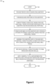
- Figure 6 is a simplified process flow chart 600 illustrating an example method for fabricating waveguide shielding walls at a waveguide interface of an integrated circuit package assembly.
- the description is intended merely to facilitate understanding of various exemplary embodiments and not by way of limitation.
- the steps may be provided in any desired order. Since the steps illustrated in Figure 6 and described below are provided by way of example only, it will be appreciated that the sequence of illustrated steps may be modified, reduced or augmented in keeping with the alternative embodiments of the disclosure so that the method may include additional steps, omit certain steps, substitute or alter certain steps, or perform certain steps in an order different than that illustrated in Figure 6 .
- the methodology of the present invention may be thought of as performing the identified sequence of steps in the order depicted, though the steps may also be performed in parallel, in a different order, or as independent operations that are combined.
- a printed circuit board (PCB) substrate is provided at step 602.
- the PCB substrate mat be an epoxy-based substrate, such as FR-4 epoxy for example, but any suitable mounting substrate element may be used.
- one or more waveguide apertures are formed in the PCB substrate.
- a masked etching process may be used to form the waveguide apertures as through holes in the PCB substrate.
- the PCB substrate may be formed as a molded structure in which waveguide apertures are formed as integral openings extending between opposed surfaces of the PCB substrate.
- the waveguide apertures may be formed by mechanical techniques (e.g., drilling) and/or chemical techniques (e.g., etching). Each waveguide aperture extends through the PCB substrate along an aperture axis so as to define inwardly-facing sidewalls in the PCB substrate.
- one or more conductive layers are patterned on at least a first surface of the PCB substrate.
- the conductive layer(s) are suitable for carrying electrical signals thereon, and may include a metallic material, such as copper, gold, aluminum of the like.
- each conductive layer is formed by bonding, sputtering depositing, or electroplating a layer of copper over the entire PCB substrate, sometimes on both sides. Subsequently, any suitable photolithographic process may be applied to pattern and selectively etch the conductive layer(s), thereby forming a conductive pattern of landing pads and trace lines.
- the conductive pattern of landing pads and trace lines can be made by adding traces to the bare PCB substrate (or a substrate with a very thin layer of copper) usually by a process of multiple electroplating steps.
- each waveguide aperture is surrounded at its periphery by a patterned conductive layer which includes defined landing pads which are connected with solder bridge trace elements, as described hereinabove.
- a patterned solder mask is formed on the PCB substrate with openings which expose the patterned conductive landing pads and shield wall traces on the PCB substrate.
- the patterned solder mask is formed by applying a solder masking layer to cover at least the first surface of the PCB substrate, and then any suitable photolithographic process may be applied to selectively expose and develop the solder masking layer so that solder mask openings are formed to expose the conductive pattern of landing pads and trace lines.
- the PCB substrate is assembled with an integrated circuit package having a solder ball conductor array aligned for contact with the conductive pattern of landing pads and trace lines formed on the PCB substrate.
- the IC package includes an antenna that is positioned in alignment with a waveguide aperture.
- the PCB substrate is affixed to the IC package by using any suitable adhesive mechanism, such as adhering the solder ball conductor array to the conductive landing pads on the PCB substrate.
- a stencil may be used to apply solder paste on the conductive pattern of the trace lines.
- the assembly step results in the attachment of solder ball conductors to the conductive pattern of landing pads surrounding the periphery of each waveguide aperture.
- a heat reflow process is applied to the solder ball conductor array to form a waveguide shielding wall around each waveguide aperture.
- the heat reflow is a thermal processing step having a controlled duration and temperature which allows individual solder ball conductors formed on the conductive pattern of landing pads to reflow and join together over the trace lines when forming the waveguide shielding walls.
- the reflow solder balls (and any solder paste applied to the trace lines) reflow to form a fully closed solder waveguide walls which shield the RF waveguide apertures in the PCB substrate from leakage and/or external interference.
- an underfill material or layer is applied to fill the gaps between the conductive solder balls attaching the PCB substrate and IC package. While any suitable underfill application process may be used, the underfill layer may be injected between the PCB substrate and the IC package from one or more external injection sites to help bond the IC package to the PCB substrate and to reinforce the solder bumps, thereby improving the reliability of the packaged assembly. However, the fully closed solder waveguide walls prevent underfill material from intruding into the waveguide apertures.
- the fabrication method ends at step 609.
- the PCB substrate is provided with at least a first waveguide aperture and a conductive pattern disposed on a first surface of the PCB substrate, where the conductive pattern includes a plurality of landing pads disposed around peripheral edges of the first waveguide aperture and connected to one another by trace lines.
- the disclosed methodology also includes forming a patterned solder mask layer over the first surface of the PCB substrate, where the patterned solder mask layer includes a plurality of mask openings corresponding in location to the plurality of landing pads and the trace lines.
- the landing pads in the conductive pattern are connected by straight trace lines to form solder bridges between the plurality of landing pads disposed around peripheral edges of the first waveguide aperture. In other embodiments, the landing pads in the conductive pattern are connected by curved trace lines to form solder bridge springs between the plurality of landing pads disposed around peripheral edges of the first waveguide aperture. In other embodiments, the landing pads disposed around peripheral edges of the first waveguide aperture include a plurality of patterned sidewall plating layers formed on the first surface and extending down interior sidewalls of the first waveguide aperture.
- the disclosed methodology includes attaching a plurality of solder balls to the PCB substrate by affixing a solder ball to each landing pad through a corresponding mask opening so that the first waveguide aperture is surrounded by solder balls having a predetermined minimum spacing distance between adjacent solder balls.
- the solder balls are attached to the PCB substrate by securing the first surface of the PCB substrate to the solder balls which are affixed to an integrated circuit die package which includes an antenna which is aligned to send or receive radio frequency signals through the first waveguide aperture.
- the solder balls are attached to the PCB substrate by printing solder paste on the trace lines to facilitate reflow of the plurality of solder balls along the trace lines during heating.
- the disclosed methodology also includes heating the plurality of solder balls and the PCB substrate to a predefined temperature for a predefined duration to reflow the plurality of solder balls along the trace lines to form a fully closed solder waveguide shielding wall disposed around peripheral edges of the first waveguide aperture.
- the disclosed methodology also includes injecting an underfill adhesive material to surround the plurality of solder balls such that the fully closed solder waveguide shielding wall prevents the underfill adhesive material from intruding into the first waveguide aperture.
- the packaged semiconductor device includes a printed circuit board substrate having at least a first waveguide aperture extending between first and second surfaces of the printed circuit board substrate.
- one or more conductive sidewall plating layers are formed on interior sidewalls of the first waveguide aperture.
- the packaged semiconductor device includes a patterned conductive layer formed on the first surface of the printed circuit board substrate with a conductive material (e.g., copper) to define a first plurality of landing pads connected to one another by trace lines and disposed around peripheral edges of the first waveguide aperture.
- a conductive material e.g., copper
- the first plurality of landing pads are connected by straight trace lines to form solder bridges between the first plurality of landing pads disposed around peripheral edges of the first waveguide aperture. In other embodiments, the first plurality of landing pads are connected by curved trace lines to form solder bridge springs between the first plurality of landing pads disposed around peripheral edges of the first waveguide aperture.
- the packaged semiconductor device includes a patterned solder mask layer formed on the first surface of the printed circuit board substrate with a plurality of mask openings corresponding in location to the first plurality of landing pads and the trace lines. The packaged semiconductor device also includes a semiconductor device having a second plurality of landing pads formed on a first surface of the semiconductor device.
- the semiconductor device is a radio frequency integrated circuit with an antenna formed on the first surface of the semiconductor device such that the antenna is aligned to send or receive radio frequency signals through the first waveguide aperture and the waveguide transition structure.
- the packaged semiconductor device includes a fully closed solder waveguide shielding wall attaching the patterned conductive layer to the second plurality of landing pads and disposed around peripheral edges of the first waveguide aperture to form a waveguide transition structure between the printed circuit board substrate and the semiconductor device.
- the fully closed solder waveguide shielding wall is formed with a plurality of reflowed solder balls which are attached to the first plurality of landing pads and trace lines to form a closed solder wall between the printed circuit board substrate and the semiconductor device to reduce signal leakage to and from any radio frequency signal transmitted through the first waveguide aperture.
- the fully closed solder waveguide shielding wall is formed with a plurality of reflowed solder balls which form a closed solder wall ring having interior sidewalls that are aligned or substantially aligned with interior sidewalls of the first waveguide aperture.
- the packaged semiconductor device includes an underfill adhesive material formed between the printed circuit board substrate and the semiconductor device to surround the fully closed solder waveguide shielding wall without intruding into the first waveguide aperture.
- the integrated circuit package assembly includes an integrated circuit chip package having a plurality of radio frequency coupling structures disposed on a first surface of the integrated circuit chip.
- the integrated circuit package assembly includes a carrier substrate having a plurality of waveguide openings which extend between first and second opposed surfaces of the carrier substrate and which are aligned, respectively, with the plurality of radio frequency coupling structures.
- the integrated circuit package assembly also includes a plurality of reflow solder waveguide shielding walls attaching the integrated circuit chip package to the carrier substrate, where each reflow solder waveguide shielding wall is disposed around peripheral edges of a corresponding waveguide opening formed in the carrier substrate to prevent signal leakage, or at least substantially so, to and from any radio frequency signal transmitted through said corresponding waveguide opening.
- each reflow solder waveguide shielding wall is a fully closed reflow solder waveguide shielding wall that fully surrounds the peripheral edges of the corresponding waveguide opening, or is a reflow solder waveguide shielding wall that includes a discontinuity or gap but still surrounds, or substantially surrounds, the peripheral edges of the corresponding waveguide opening.
- the plurality of reflow solder waveguide shielding walls are each connected to a predetermined reference or ground voltage.
- integrated circuit package assembly also includes a patterned conductive layer formed on the first surface of the carrier substrate to define, around peripheral edges of each of the plurality of waveguide openings, a first plurality of copper landing pads connected to one another by copper trace lines.
- solder ball grid array may be placed with the regular grid spacing.
- slight deviations of the solder ball grid array positioning can be used to facilitate board assembly and solder reflow performance, such as by placing the landing pads and solder balls at closer spacing to enable solder reflow and joining of solder balls.
Landscapes
- Engineering & Computer Science (AREA)
- Microelectronics & Electronic Packaging (AREA)
- Manufacturing & Machinery (AREA)
- Physics & Mathematics (AREA)
- Electromagnetism (AREA)
- Geometry (AREA)
- Structure Of Printed Boards (AREA)
- Electric Connection Of Electric Components To Printed Circuits (AREA)
Applications Claiming Priority (1)
| Application Number | Priority Date | Filing Date | Title |
|---|---|---|---|
| US17/726,426 US11963291B2 (en) | 2022-04-21 | 2022-04-21 | Efficient wave guide transition between package and PCB using solder wall |
Publications (1)
| Publication Number | Publication Date |
|---|---|
| EP4266484A1 true EP4266484A1 (de) | 2023-10-25 |
Family
ID=86053752
Family Applications (1)
| Application Number | Title | Priority Date | Filing Date |
|---|---|---|---|
| EP23167569.5A Withdrawn EP4266484A1 (de) | 2022-04-21 | 2023-04-12 | Effizienter wellenleiterübergang zwischen gehäuse und leiterplatte unter verwendung einer lötwand |
Country Status (2)
| Country | Link |
|---|---|
| US (1) | US11963291B2 (de) |
| EP (1) | EP4266484A1 (de) |
Families Citing this family (2)
| Publication number | Priority date | Publication date | Assignee | Title |
|---|---|---|---|---|
| KR102896542B1 (ko) * | 2020-11-06 | 2025-12-08 | 삼성전자주식회사 | 솔더 월을 포함하는 전자 장치 |
| US12315999B2 (en) * | 2022-07-15 | 2025-05-27 | Aptiv Technologies AG | Solderable waveguide antenna |
Citations (2)
| Publication number | Priority date | Publication date | Assignee | Title |
|---|---|---|---|---|
| US20070085635A1 (en) * | 2000-10-06 | 2007-04-19 | Mitsubishi Denki Kabushiki Kaisha | Waveguide coupler |
| US20130012145A1 (en) * | 2010-03-24 | 2013-01-10 | Nec Corporation | Radio module and manufacturing method therefor |
Family Cites Families (22)
| Publication number | Priority date | Publication date | Assignee | Title |
|---|---|---|---|---|
| US5969461A (en) | 1998-04-08 | 1999-10-19 | Cts Corporation | Surface acoustic wave device package and method |
| FR2786959B1 (fr) | 1998-12-08 | 2001-05-11 | Thomson Csf | Composant a ondes de surface encapsule et procede de fabrication collective |
| US7547579B1 (en) | 2000-04-06 | 2009-06-16 | Micron Technology, Inc. | Underfill process |
| US6800946B2 (en) | 2002-12-23 | 2004-10-05 | Motorola, Inc | Selective underfill for flip chips and flip-chip assemblies |
| US7105931B2 (en) | 2003-01-07 | 2006-09-12 | Abbas Ismail Attarwala | Electronic package and method |
| AT413891B (de) * | 2003-12-29 | 2006-07-15 | Austria Tech & System Tech | Leiterplattenelement mit wenigstens einem licht-wellenleiter sowie verfahren zur herstellung eines solchen leiterplattenelements |
| MY158939A (en) | 2008-10-21 | 2016-11-30 | Atotech Deutschland Gmbh | Method to form solder deposits on substrates |
| EP2337068A1 (de) | 2009-12-18 | 2011-06-22 | Nxp B.V. | Im Voraus gelötete leitungslose Kapselung |
| US8574960B2 (en) | 2010-02-03 | 2013-11-05 | Stats Chippac, Ltd. | Semiconductor device and method of forming cavity adjacent to sensitive region of semiconductor die using wafer-level underfill material |
| US8169060B2 (en) | 2010-03-29 | 2012-05-01 | Infineon Technologies Ag | Integrated circuit package assembly including wave guide |
| US8796075B2 (en) | 2011-01-11 | 2014-08-05 | Nordson Corporation | Methods for vacuum assisted underfilling |
| US9136230B2 (en) | 2013-03-28 | 2015-09-15 | Broadcom Corporation | IC package with integrated waveguide launcher |
| US8860212B1 (en) | 2013-04-15 | 2014-10-14 | Freescale Semiconductor, Inc. | Fluid cooled semiconductor die package |
| US9090454B2 (en) | 2013-08-27 | 2015-07-28 | Freescale Semiconductor, Inc. | Sequential wafer bonding |
| US9237647B2 (en) | 2013-09-12 | 2016-01-12 | Taiwan Semiconductor Manufacturing Company, Ltd. | Package-on-package structure with through molding via |
| US9627346B2 (en) | 2013-12-11 | 2017-04-18 | Taiwan Semiconductor Manufacturing Company, Ltd. | Underfill pattern with gap |
| US10103447B2 (en) | 2014-06-13 | 2018-10-16 | Nxp Usa, Inc. | Integrated circuit package with radio frequency coupling structure |
| US9904776B2 (en) | 2016-02-10 | 2018-02-27 | Taiwan Semiconductor Manufacturing Company, Ltd. | Fingerprint sensor pixel array and methods of forming same |
| JP6643714B2 (ja) * | 2016-03-10 | 2020-02-12 | 富士通株式会社 | 電子装置及び電子機器 |
| US10802375B2 (en) * | 2017-09-15 | 2020-10-13 | Samsung Electronics Co., Ltd. | Optically-controlled switch |
| US11527808B2 (en) | 2019-04-29 | 2022-12-13 | Aptiv Technologies Limited | Waveguide launcher |
| US11557491B2 (en) | 2019-10-31 | 2023-01-17 | Nxp B.V. | Selective underfill assembly and method therefor |
-
2022
- 2022-04-21 US US17/726,426 patent/US11963291B2/en active Active
-
2023
- 2023-04-12 EP EP23167569.5A patent/EP4266484A1/de not_active Withdrawn
Patent Citations (2)
| Publication number | Priority date | Publication date | Assignee | Title |
|---|---|---|---|---|
| US20070085635A1 (en) * | 2000-10-06 | 2007-04-19 | Mitsubishi Denki Kabushiki Kaisha | Waveguide coupler |
| US20130012145A1 (en) * | 2010-03-24 | 2013-01-10 | Nec Corporation | Radio module and manufacturing method therefor |
Also Published As
| Publication number | Publication date |
|---|---|
| US20230345623A1 (en) | 2023-10-26 |
| US11963291B2 (en) | 2024-04-16 |
Similar Documents
| Publication | Publication Date | Title |
|---|---|---|
| US8592959B2 (en) | Semiconductor device mounted on a wiring board having a cap | |
| US7102230B2 (en) | Circuit carrier and fabrication method thereof | |
| US20060131758A1 (en) | Anchored non-solder mask defined ball pad | |
| EP4266484A1 (de) | Effizienter wellenleiterübergang zwischen gehäuse und leiterplatte unter verwendung einer lötwand | |
| EP1207727B1 (de) | Nachgiebiger Laminatverbinder | |
| KR100483642B1 (ko) | 반도체장치및반도체장치의제조방법 | |
| KR20090042777A (ko) | 반도체 플립칩 패키지를 위한 기판 및 공정 | |
| US9681543B2 (en) | Method for making electronic device with cover layer with openings and related devices | |
| US20080157295A1 (en) | Methods and apparatus for multichip module packaging | |
| US20200251436A1 (en) | Semiconductor device package with improved die pad and solder mask design | |
| EP0920711A1 (de) | Interfacestrukturen für elektronische anordnungen | |
| US9589908B1 (en) | Methods to improve BGA package isolation in radio frequency and millimeter wave products | |
| US20040012097A1 (en) | Structure and method for fine pitch flip chip substrate | |
| KR100250562B1 (ko) | 반도체장치 | |
| US6402970B1 (en) | Method of making a support circuit for a semiconductor chip assembly | |
| KR100300922B1 (ko) | 반도체장치 | |
| US7036712B2 (en) | Methods to couple integrated circuit packages to bonding pads having vias | |
| EP3971963B1 (de) | Halbleitergehäuseanordnung | |
| KR20160084666A (ko) | 인쇄회로기판, 반도체 패키지 및 이들의 제조방법 | |
| US9060430B1 (en) | Shielded trace structure and fabrication method | |
| EP2146557B1 (de) | Integrierte Mikrowellenschaltung | |
| US10531558B2 (en) | Electronic module having electromagnetic shielding structure and manufacturing method thereof | |
| JPH10178144A (ja) | Bga型電子部品の同軸電極構造 | |
| JP4519102B2 (ja) | 導波管接続構造とその製造方法 | |
| JP2004153179A (ja) | 半導体装置および電子装置 |
Legal Events
| Date | Code | Title | Description |
|---|---|---|---|
| STAA | Information on the status of an ep patent application or granted ep patent |
Free format text: STATUS: THE APPLICATION HAS BEEN PUBLISHED |
|
| PUAI | Public reference made under article 153(3) epc to a published international application that has entered the european phase |
Free format text: ORIGINAL CODE: 0009012 |
|
| AK | Designated contracting states |
Kind code of ref document: A1 Designated state(s): AL AT BE BG CH CY CZ DE DK EE ES FI FR GB GR HR HU IE IS IT LI LT LU LV MC ME MK MT NL NO PL PT RO RS SE SI SK SM TR |
|
| STAA | Information on the status of an ep patent application or granted ep patent |
Free format text: STATUS: REQUEST FOR EXAMINATION WAS MADE |
|
| 17P | Request for examination filed |
Effective date: 20240425 |
|
| RBV | Designated contracting states (corrected) |
Designated state(s): AL AT BE BG CH CY CZ DE DK EE ES FI FR GB GR HR HU IE IS IT LI LT LU LV MC ME MK MT NL NO PL PT RO RS SE SI SK SM TR |
|
| STAA | Information on the status of an ep patent application or granted ep patent |
Free format text: STATUS: THE APPLICATION IS DEEMED TO BE WITHDRAWN |
|
| 18D | Application deemed to be withdrawn |
Effective date: 20240426 |