EP4266313A1 - Direktzugriffsspeicher und zugehöriges verfahren zur verwaltung eines direktzugriffsspeichers - Google Patents
Direktzugriffsspeicher und zugehöriges verfahren zur verwaltung eines direktzugriffsspeichers Download PDFInfo
- Publication number
- EP4266313A1 EP4266313A1 EP23163536.8A EP23163536A EP4266313A1 EP 4266313 A1 EP4266313 A1 EP 4266313A1 EP 23163536 A EP23163536 A EP 23163536A EP 4266313 A1 EP4266313 A1 EP 4266313A1
- Authority
- EP
- European Patent Office
- Prior art keywords
- clock
- input
- output
- logic
- memory
- Prior art date
- Legal status (The legal status is an assumption and is not a legal conclusion. Google has not performed a legal analysis and makes no representation as to the accuracy of the status listed.)
- Pending
Links
Images








Classifications
-
- G—PHYSICS
- G11—INFORMATION STORAGE
- G11C—STATIC STORES
- G11C29/00—Checking stores for correct operation ; Subsequent repair; Testing stores during standby or offline operation
- G11C29/02—Detection or location of defective auxiliary circuits, e.g. defective refresh counters
- G11C29/023—Detection or location of defective auxiliary circuits, e.g. defective refresh counters in clock generator or timing circuitry
-
- G—PHYSICS
- G11—INFORMATION STORAGE
- G11C—STATIC STORES
- G11C29/00—Checking stores for correct operation ; Subsequent repair; Testing stores during standby or offline operation
- G11C29/04—Detection or location of defective memory elements, e.g. cell constructio details, timing of test signals
- G11C29/08—Functional testing, e.g. testing during refresh, power-on self testing [POST] or distributed testing
- G11C29/12—Built-in arrangements for testing, e.g. built-in self testing [BIST] or interconnection details
- G11C29/18—Address generation devices; Devices for accessing memories, e.g. details of addressing circuits
- G11C29/30—Accessing single arrays
- G11C29/32—Serial access; Scan testing
-
- G—PHYSICS
- G06—COMPUTING OR CALCULATING; COUNTING
- G06F—ELECTRIC DIGITAL DATA PROCESSING
- G06F12/00—Accessing, addressing or allocating within memory systems or architectures
- G06F12/02—Addressing or allocation; Relocation
- G06F12/0223—User address space allocation, e.g. contiguous or non contiguous base addressing
- G06F12/023—Free address space management
-
- G—PHYSICS
- G11—INFORMATION STORAGE
- G11C—STATIC STORES
- G11C11/00—Digital stores characterised by the use of particular electric or magnetic storage elements; Storage elements therefor
- G11C11/21—Digital stores characterised by the use of particular electric or magnetic storage elements; Storage elements therefor using electric elements
- G11C11/34—Digital stores characterised by the use of particular electric or magnetic storage elements; Storage elements therefor using electric elements using semiconductor devices
- G11C11/40—Digital stores characterised by the use of particular electric or magnetic storage elements; Storage elements therefor using electric elements using semiconductor devices using transistors
- G11C11/41—Digital stores characterised by the use of particular electric or magnetic storage elements; Storage elements therefor using electric elements using semiconductor devices using transistors forming static cells with positive feedback, i.e. cells not needing refreshing or charge regeneration, e.g. bistable multivibrator or Schmitt trigger
- G11C11/413—Auxiliary circuits, e.g. for addressing, decoding, driving, writing, sensing, timing or power reduction
- G11C11/417—Auxiliary circuits, e.g. for addressing, decoding, driving, writing, sensing, timing or power reduction for memory cells of the field-effect type
-
- G—PHYSICS
- G11—INFORMATION STORAGE
- G11C—STATIC STORES
- G11C11/00—Digital stores characterised by the use of particular electric or magnetic storage elements; Storage elements therefor
- G11C11/21—Digital stores characterised by the use of particular electric or magnetic storage elements; Storage elements therefor using electric elements
- G11C11/34—Digital stores characterised by the use of particular electric or magnetic storage elements; Storage elements therefor using electric elements using semiconductor devices
- G11C11/40—Digital stores characterised by the use of particular electric or magnetic storage elements; Storage elements therefor using electric elements using semiconductor devices using transistors
- G11C11/41—Digital stores characterised by the use of particular electric or magnetic storage elements; Storage elements therefor using electric elements using semiconductor devices using transistors forming static cells with positive feedback, i.e. cells not needing refreshing or charge regeneration, e.g. bistable multivibrator or Schmitt trigger
- G11C11/413—Auxiliary circuits, e.g. for addressing, decoding, driving, writing, sensing, timing or power reduction
- G11C11/417—Auxiliary circuits, e.g. for addressing, decoding, driving, writing, sensing, timing or power reduction for memory cells of the field-effect type
- G11C11/419—Read-write [R-W] circuits
-
- G—PHYSICS
- G11—INFORMATION STORAGE
- G11C—STATIC STORES
- G11C19/00—Digital stores in which the information is moved stepwise, e.g. shift registers
- G11C19/28—Digital stores in which the information is moved stepwise, e.g. shift registers using semiconductor elements
- G11C19/287—Organisation of a multiplicity of shift registers
-
- G—PHYSICS
- G11—INFORMATION STORAGE
- G11C—STATIC STORES
- G11C29/00—Checking stores for correct operation ; Subsequent repair; Testing stores during standby or offline operation
- G11C29/04—Detection or location of defective memory elements, e.g. cell constructio details, timing of test signals
- G11C29/08—Functional testing, e.g. testing during refresh, power-on self testing [POST] or distributed testing
- G11C29/12—Built-in arrangements for testing, e.g. built-in self testing [BIST] or interconnection details
- G11C29/12015—Built-in arrangements for testing, e.g. built-in self testing [BIST] or interconnection details comprising clock generation or timing circuitry
-
- G—PHYSICS
- G11—INFORMATION STORAGE
- G11C—STATIC STORES
- G11C29/00—Checking stores for correct operation ; Subsequent repair; Testing stores during standby or offline operation
- G11C29/04—Detection or location of defective memory elements, e.g. cell constructio details, timing of test signals
- G11C29/08—Functional testing, e.g. testing during refresh, power-on self testing [POST] or distributed testing
- G11C29/12—Built-in arrangements for testing, e.g. built-in self testing [BIST] or interconnection details
- G11C29/18—Address generation devices; Devices for accessing memories, e.g. details of addressing circuits
- G11C29/20—Address generation devices; Devices for accessing memories, e.g. details of addressing circuits using counters or linear-feedback shift registers [LFSR]
-
- G—PHYSICS
- G06—COMPUTING OR CALCULATING; COUNTING
- G06F—ELECTRIC DIGITAL DATA PROCESSING
- G06F2212/00—Indexing scheme relating to accessing, addressing or allocation within memory systems or architectures
- G06F2212/20—Employing a main memory using a specific memory technology
- G06F2212/202—Non-volatile memory
-
- G—PHYSICS
- G11—INFORMATION STORAGE
- G11C—STATIC STORES
- G11C29/00—Checking stores for correct operation ; Subsequent repair; Testing stores during standby or offline operation
- G11C29/04—Detection or location of defective memory elements, e.g. cell constructio details, timing of test signals
- G11C29/08—Functional testing, e.g. testing during refresh, power-on self testing [POST] or distributed testing
- G11C29/12—Built-in arrangements for testing, e.g. built-in self testing [BIST] or interconnection details
- G11C29/18—Address generation devices; Devices for accessing memories, e.g. details of addressing circuits
- G11C29/30—Accessing single arrays
- G11C2029/3202—Scan chain
-
- G—PHYSICS
- G11—INFORMATION STORAGE
- G11C—STATIC STORES
- G11C29/00—Checking stores for correct operation ; Subsequent repair; Testing stores during standby or offline operation
- G11C29/04—Detection or location of defective memory elements, e.g. cell constructio details, timing of test signals
- G11C29/08—Functional testing, e.g. testing during refresh, power-on self testing [POST] or distributed testing
- G11C29/12—Built-in arrangements for testing, e.g. built-in self testing [BIST] or interconnection details
- G11C29/46—Test trigger logic
Definitions
- Embodiments of the present disclosure relate to a Random Access Memory.
- Embodiments of the present disclosure relate in particular to Random Access Memory designed for testability, in particular to Single Port Random Access Memory and Dual Port Random Access Memory.
- the RAM (Random Access Memory) memory comprises an analog portion, in particular represented by the memory array, and includes also boundary logic that is digital, that is usually specifically designed in order to optimize the device area impact.
- This circuit differently from the digital logic of the device, tested with SCAN Architecture, requires a specific Built-In Self-Test hardware controller to ensure the quality.
- a Built-In Self Test hardware controller together with the embedded RAM control logic might have a not negligible area overhead with respect to the RAM matrix (i.e. in some cases the BIST might have area size similar to the RAM one).
- a known solution relies on replacing the RAM memory matrix with standard Flip-Flop and adding the required digital control logic to obtain a same timing waveform as specified in the RAM datasheet.
- a Random Access Memory comprising an array of storage elements (L) arranged in rows and columns, the rows of storage elements identifying respective memory locations, wherein said array of storage elements comprise an array of D type latches, receiving at their data input bits of the data to be stored and at their clock input a gated clock signal corresponding to the memory location to which they belong.
- a column in said array of D type latches comprise D scan ready flip flops in place of D type latches.
- a column of D flip flops is added to said array of D type latches.
- the outputs of the latches of an address location are supplied to a data selector block selecting latch data bits corresponding to the address bits bus signal.
- said random access memory comprise a clock input logic configured to provide respective gated clocks for each memory location in the array of D type latches said clock input logic comprising
- said clock input logic comprises a logic to enable testing comprising an OR gate receiving at its inputs test a test mode signal commanding the operation in test mode of the memory and a scan enable signal enabling an ATPG scan in test mode, the output of said OR gate being supplied at one input, in particular of a OR gate or a NOR gate, of said clock gating cells, another input receiving said one hot format addresses, so that if the scan enable signal is active, i.e., logic one, all the clock gating cells clock all the latches of the array of latches.
- each of said clock gating cells comprises
- the memory comprises a mask generator comprising a multiplexer receiving on one input the latch output bits read from the latch array and on the other the bus carrying the data to be stored, while sampled mask bits are supplied as selection signal of the multiplexer, the multiplexer being configured to select as masked data bits, for the not asserted sampled mask bits said bus carrying the data to be stored (SDB), and, for the asserted sampled mask bits said latch output bits.
- a mask generator comprising a multiplexer receiving on one input the latch output bits read from the latch array and on the other the bus carrying the data to be stored, while sampled mask bits are supplied as selection signal of the multiplexer, the multiplexer being configured to select as masked data bits, for the not asserted sampled mask bits said bus carrying the data to be stored (SDB), and, for the asserted sampled mask bits said latch output bits.
- said mask generator further comprise a mask bypass multiplexer which receives at input the bus carrying the data to be stored and the masked data bits and selects the output of the mask generator on the basis of signal indicating masking mode or not masking mode.
- said mask generator comprise an array of flip flops to resample the masked data bits with the clock edge, in particular clock rising edge.
- said memory comprises an input sampling logic comprising rows of cascaded scan ready delay flip flops clocked by the write clock signal, each row sampling respectively the write address bus, the data bus and the mask bus if present and a sampling output logic configured to receive the latch output bits as input of a selection module, in particular a multiplexer, receiving also as feedback the output of the sampling output logic, configured to select the latch output bits depending on the value of a read enable signal, the output bits of the selection module being coupled to the data input of respective resampling flip flops which output forms the output of the sampling output logic.
- said random access memory is a Dual port RAM, comprising a further sampling input logic, which samples read signals with a read clock and comprising a further sampling output logic also sampling read signals with said read clock.
- the flip-flops of the input sampling logic, output sampling logic, and mask generator if present are scan ready D flip flops which can be coupled by a scan path, in particular one or more scan chains, suitable to be coupled to an ATPG generator in a test mode.
- said latches of said array of D type latches are transparent, so that its output has the same value of its input, on the high logic value of the clock, if the clock in the memory is sampled on the falling edge in said memory, and on the low logic value of the clock, if the clock in the memory is sampled on the rising edge in said memory.
- the solution here described refers also to a method for managing a Random Access Memory according to any of the embodiments comprising the operations indicated in one or more of said embodiments.
- the present disclosure also provides solutions regarding a method for managing a Random Access Memory according to any of the embodiments comprising the operations indicated in one or more of said embodiments.
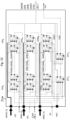
- FIG 1 it is shown an architecture, indicated by the numerical reference 10, of a Single Port RAM memory according to the solution here described.
- the block indicated with 10 defines the boundary of the Single Port RAM which includes a flip-flops input sampling logic 11, to sample the input boundary signals with a clock signal CLK, a clock gate control logic 12, to provide a latch based matrix 13 with respective gated clock signals GC for each address associated to a location in said latch matrix 13, which is the block where the data are stored, then a flip-flops output sampling logic 14, to sample the output boundary signals, and optional mask data management module 15, required only when the RAM 10 has masking capability, i.e. the capability of masking the writing of some data bits so that they can maintain the status they already have.
- mask data management module required only when the RAM 10 has masking capability, i.e. the capability of masking the writing of some data bits so that they can maintain the status they already have.
- the matrix 13 is latched based in that comprises as memory storage elements latches, in particular D latches. This as opposed to matrix having as storage elements flip-flops which are in general combination of latches, in particular a combination of two cascaded latches with clock inverted to have master-slave behavior.
- the Single Port RAM 10 includes as input boundary signals the interface signals that are usually available for such type of memory, namely:
- the Single Port memory 10 then further includes as input boundary signals, test signals, specifically Scan In signal SIS and Scan Out SOS, which are test signals to integrate scan chains structure in the device.
- test signals specifically Scan In signal SIS and Scan Out SOS, which are test signals to integrate scan chains structure in the device.
- Scan In signal SIS is indicated the signal of the scan path inputting a block
- Scan Out signal SOS is indicated the signal of the Scan path outputting a block.
- a scan enable signal SES is also received at input of RAM 10 which is a test signal to define the shift versus capture operation of the scan chain structure, while the reset signal RST, as better illustrated in the following, is used to initialize the status of the internal Flip-Flops (FF) in block 11, as well as in blocks 14 and 15. All the flip flops of the RAM 10 are SCAN ready and can be inserted in the scan chain structure allowing to reach the ATPG (Automatic Test Pattern Generation) coverage target.
- a scan ready flip-flop in general is a D flip-flop with a 2x1 multiplexer added at its input D, as better seen in figure 2 , for instance in flip flop FFA0. This type of flip flop is oftentimes also called scan flip flop, or SFF.
- test enable TE input is provided (which is coupled to the scan enable signals, SES) and Test In TI (which is coupled to the scan in signal SIS).
- test enable TE when test enable TE is equal to logic one, the shift operation occurs -not simply Test mode- (TI sampled) in the scan chains (to serially load/unload) while when test enable TE is equal to logic zero, the functional mode is enabled (input D sampled).
- the TE pin is used to control the multiplexer of the Scan ready flip flop, i.e., used as selection bit.
- all the scan ready flip flops of block 11 have also a reset pin coupled to the reset signal RST.
- the input sampling block 11 which receives the input signals indicated above, and comprises a first row of address resampling scan ready delay flip flops FFA, from FFA 0 to FFA Y for each of the Y+1 bits on the AD bus in order which is brought to the data input D of the respective flip flop FFA j , j index from 0 to Y.
- the Scan in signal SIS is brought to the TI input of the first flip FFA 0 , while output SO is coupled to the TI input of the following flip flop, and so on, this being exemplary of a possible way according to which the flip flops are cascaded with respect to the scan in signal SIS, i.e.
- the Scan Enable signal SES is brought in parallel to all the flip flops FFA, to the TE input.
- the clock signal CLK is brought to their clock input CK.
- On the output Q of each address resampling flip flop FFA j is a sampled address bit SAB j , which is collected by a bus of sampled address bits SAB, carrying the Y+1 bits SAB 0 ... SAB Y which are used to obtain the memory locations ML0...MLW in the latched memory 13.
- the memory locations ML0...MLW are in a number which is a power of two with respect to the corresponding Y+1 bits SABo... SAB Y , e.g., 4 SAB bits means 16.
- block 11 includes a second row of data resampling scan ready flip flops FFD, from FFD 0 to FFD X , for each of the X+1 bits on the data bus WB in order, which are brought to the data input D of the respective flip flop FFD i , I index from 0 to X.
- On the output Q of each data resampling flip flop FFD i is a sampled data bit SDB i , which is collected by a bus of sampled data bits SDB, carrying the X+1 data bits SDB 0 ... SDB X .
- the TI input of the first flip FFD0 is coupled to the output SO of the last address resampling flip flop FFA Y , then the other flip flops are cascaded in the same way of the address flip flops for the scan daisy chain, the Scan Enable signal SES being also brought in parallel to all the flip flops FFD, to the TE input and the clock signal CLK being brought to their clock input CK.
- block 11 includes optionally a third row of mask resampling scan ready flip flops FFM, from FFM 0 to FFMx, for each of the X+1 bits on the mask bus MB in order, which are brought to the data input D of the respective flip flop FFM i .
- On the output Q of each data resampling flip flop FFM i is a sampled mask bit SMB i , which is collected by a bus of sampled mask bits SMB, carrying the X+1 mask bits SMB 0 ... SMBx.
- the TI input of the first flip FFM0 is coupled to the output SO of the last data resampling flip flop FFDx, then the other flip flops are cascaded with respect to the scan in signal SIS in the same way of the address flip flops for the scan daisy chain, the Scan Enable signal SES being also brought in parallel to all the flip flops FFD, to the TE input and the clock signal CLK being brought to their clock input CK.
- the scan path associated to the Scan In signal SIS is shown by a dashed line in the figures, the Scan Enable signal SES in solid line.
- the clock CLK is represented by a point dash line.
- Block 11 comprises a further sampled write enable signal SWE, as output, which is the sampled AND, in a AND port 111, between the write enable signal WES and the chip select signal CSS and is used to validate the Write Enable operation only when Chip Select is active.
- the sampling of the output of the AND gate 111 is performed by a first test flip flop FFT1, also a scan ready flip flop, which receives the output of such AND 111 in the data D input and outputs on the Q pin the sampled write enable signal SWE.
- a FF Sampled Test Mode signal STM is provided as the output of block 11, outputted by a second test flip-flop FFT2, also a scan ready flip flop like the others, with the output Q coupled to the data input D, which is not used however in functional mode, i.e. for normal operation of the RAM, but is required in ATPG Scan mode to give more flexibility to ATPG engine in managing the Enable of the Clock Gating GC included in the Clock Gate Control Block 12.
- the scan path i.e. the scan in signal SIS, in the example shown is propagated in the cascade of the first row, second row, third row of flip flops, then in FFT1 and FFT2, where, from the output SO, is brought at the output of block 11 as scan out signal SOS.
- SOS scan out signal
- RAM locations ML 0 ...ML W are values which are in a total number of 2 Y+1 .
- a one hot address decoder i.e. which outputs decoded signals in the form of sequence of bits with only one logic one, receiving the address signal SAB and sampled write enable SWE and outputting one hot decoded address signals DAB 0 ...DAB W to respective integrated clock gating cells 123 0 ...123 W , which output a respective gated clock signals GCo... GCw.
- Such sequences of bits with only one logic one are a power of two with exponent the corresponding address signal SAB, i.e. with 4 bit of address signal SAB, 16 gated clock signals GCo... GCw are generated. It may be possible that not all the memory bits are used (e.g., a memory with 13 rows has 4 SAB bits but only 13 gated clock signals GC).
- a test logic 122 receives at its input the test mode signal STM and the scan enable SES, outputting a test mode enable signal TSE.
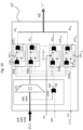
- Each clock gating cell 123 j in the example shown comprises an OR input gate 124 j receiving the decoded address DAB j and the test mode enable signal TSE and supplying its output to the data input D of a cell latch FFC j , which receives at its clock input GN the negated of the clock CLK. When clock input GN is low the latch is transparent.
- the clock CLK is brought to an input of an AND gate 125 j , which gates such clock CLK with the output of the cell latch FFC j received at its other input, thus outputting a gated address GC j , i.e. the pulse of clock CLK corresponding to the one in the corresponding one hot decoded address signals DAB j , which is thus a pulse on positive clock CLK as consequence of the FF input sampling 11 happening on the falling edge of clock CLK so that there is no timing trouble (clocks are the most critical signals and so must be managed in the cleanest way).
- the implementation of the clock gate control logic 12 shown in figure 3 may operate on clock falling edges, although in variant embodiments the clock gate control logic 12 may be rearranged to operate with all the clock edges inverted.
- the integrated clock gating cells 123 logic arrangement, of which in the figure 3 is given an example suitable for the falling edge, may be adapted accordingly to perform the integrated clock gating function.
- the OR 122 between Sampled Test Mode STM and Scan Enable signal SES is introduced, a logic gate which operates in combination with the one hot address decoder.
- Scan chain operation in ATPG involves three stages: Scan-in, Scan-capture and Scan-out.
- Scan-in involves shifting in and loading all the flip-flops with an input vector.
- the data flows from the output of one flip flop to the scan-input of the next flip flop (as depicted in Figure 2 for block 11) not unlike a shift register.
- one clock pulse also called the capture pulse
- each flip-flop samples the data as in functional mode through the combo logic connected in between the output Q of the scan FF and their input D. This is because Scan-Enable SES is off.
- the data is then shifted out and the signature is compared with the expected signature.
- the signal Scan enable SES is active, i.e. logic one, and so, even if the content of the Sampled Test Mode STM might toggle (it is itself part of the scan chain or chains), the output of the OR 122 is always active, i.e., logic one.
- This condition forces all the clock gate cells 123 active (because OR gate 124 output is always active) and so to clock all the latches of the RAM Latch matrix 13 (differently from the user or functional, or normal, mode where only one latch might be clocked).
- the ATPG apply the capture mode. This is the mode in which clock is pulsed and next state is loaded from the previous pre-loaded one through scan shift architecture.
- Scan enable is quite always NOT active and, in this condition, Sampled Test mode STM play a role.
- Scan enable is quite always NOT active and, in this condition, Sampled Test mode STM play a role.
- the latch-based matrix 13 may be implemented in three different embodiments, each having a respective difference.
- FIG 4 it is shown a first embodiment which comprises receiving signals GC, SAB and X+1 data bits SDB.
- the matrix 13 then comprises a matrix of latches L, organized in rows and columns.
- Each row of the matrix 13, corresponding to a memory location ML j , corresponding to an address SAB j comprises X+1 latches L j0 ...L jX , thus the matrix 13 comprises 2 Y+1 rows of X+1 latches, thus a matrix of latches LL 00 ...LL WX .
- Each latch LL ij comprises a gated clock input G and a latch data input D, as well as a latch output Q.
- Each row receives a gated clock GC j corresponding to the j-th address SAB j , at its gated clock input G, while the data or masked data bits, SDB, MDB are sent to the data input D of latches LL 10 ...LL WX , each latch L j0 ...L jX of a row receiving at its data input D one of the bits 0... X respectively of the data or masked data bits, SDB, MDB.
- Only the row receiving a gated clock with the positive pulse stores the SDB or MDB data.
- the latches with the clock pulse active update the status, while all the other keep the previous content of the data.
- the outputs of the latches L j0 ...L jX of an address location ML j are X+1 output bits which are supplied to a respective AND gate 132j, comprised in a data selector block 131, comprising an OR-reduce architecture, which performs a logic OR with the sampled address bits bus signal SAB.
- a respective AND gate 132j comprised in a data selector block 131, comprising an OR-reduce architecture, which performs a logic OR with the sampled address bits bus signal SAB.
- W+1 AND gates 132 0 ...132 W which outputs are sent to a multiple input OR GATE 133, which output represents the X+1 latch Data Bits LDB.
- OR-reduce is one possible architecture for this logic but also logic based on multiplexers may be used for the solution, or other logic, provided that the selected address location by SAB is visible on latch Data Bits LDB reading the related LDB latch row.
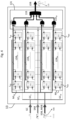
- the latch-based matrix 13 thus represents the array of memory elements, i.e. the latches LLoo... LL WX , and it is arranged so that each RAM location ML j , i.e. each latch LL 1 has its own Gated clock signal GC j enabled in a mutually exclusive mode (one hot) as depicted in the Clock gating control logic 12 description, i.e. by the decoder 121.
- the data that is to be written in each RAM location ML j depends whether the RAM 10 operates or not with the mask capability.
- the Data Mask bit MDB are only coming from the FF Input sampling logic 11 and thus data are updated on the clock CLK falling edge, as shown by the arrow in the waveform of sampled address bits SAB.
- the data selector 131 sub-block allows to propagate only the latch output Q of the selected location, i.e. latches L j0 ...L jX , that is decoded from sampled add bits signal SAB j .
- the selector 131 is designed with an OR-reduce tree, in which basically all the outputs from the not selected location, i.e. different from ML j , are forced low - this is obtained by the first AND stage 132 - while the outputs of the selected one ML j is high, and an OR 133 among all the same bit position of all the memory locations is performed so that only the one location not forced low is propagated. Note that this is a possible solution, but also other choices might be possible to implement the selector 133, such as the use of a Multiplexer or complementary solution, such as an AND-Reduce logic architecture.
- the Latch Data bits output signals LDB is updated starting from clock CLK high till the clock goes low, on which the address signal SAB might change since new operation could be applied, e.g. pipeline operations.
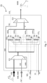
- the Mask data management block 15 shown in figure 7 , which is an optional block, aimed to manage Mask capability, is described.
- the Mask data management block 15 includes a two-way multiplexer 151, with X+1 outputs, receiving on one input the Latch Data bits output signals LDB and on the other the Sampled Data Bits SDB, while the sampled mask bits SMB are supplied as selection signal of the multiplexer 151.
- the X+1 outputs of the multiplexer 151 are supplied to the data input of respective X+1 flip flops 152 which are also scan ready flip flops with the already described inputs and outputs.
- the data output of the X+1 flip flops 152 are brought on a mask used path U to an output "Mask Bypass feature" multiplexer 153, which receives on a mask not used NU input path the Sampled Data Bits SDB directly from the input of the block 15.
- the overall behavior is equivalent to have the "Mask Bypass feature” multiplexer 153 in the "NOT used” configuration, i.e. allowing the NU path as output.
- the Output Data Mask bits MDB are fully coming from the FF input sampling logic 11 -as Sampled Data bits SDB- and are updated on the clock CLK falling edge (as shown in the SDB waveform) while if the configuration is to use mask capability (thus "Used" path U is selected) the data are coming from the output Q pin of the internal flip flops 152o... 152x.
- flip flops 152 0 ...152x are sampled on the clock rising edge and the data content depends on the status of the Mask Input multiplexer 151 (X+1 2-way Mux).
- Latch Data Bits bus LDB generated inside of the Latch Matrix 13.
- This bus has the content of selected location (Older data bits OB before any write operation, while UB indicates updated bits, only in write mode) stable and equivalent to previous data till clock CLK rising edge and so the content of the re-sampling flip flop on the rising edge allows to maintain this status since the RAM matrix 13 block writing operation is performed on the clock falling edge (when the Gated clock GCj goes from high to low logic level).
- the latches LL j0 -LL jx are transparent starting on the clock rising edge but since the Mask Data Bits MDB change on this edge and the sampling in the latch is performed at the clock falling edge, the overall write operation happens on CLK falling edge when data is stable. This allows to maintain the status of masked location bits.
- FIG 5 it is shown a second embodiment, indicate with the reference 13', of the latch matrix according to the solution here described. Analogous or corresponding elements with respect to figure 4 are indicated by the same reference.
- Such second embodiments 13' differs in that the element storing the bit 0 of each Ram Address location ML j , i.e. of each row, which is embodied a latch in the matrix 13 of figure 4 , is replaced here by a respective flip flop FF' 00 ...FF' W0 .
- the gated clock GC is brought to a clock input CP of the flip flops FF' 00 ...FF' W0 .
- any i-th bits, from 0 to X, of the rows, or memory locations ML j , j from 0 to W can be selected to replace the column of latches Loi... L Wi with a column of flip-flops FF' 0i ...FF' Wi .
- This embodiment of the matrix 13' improves the capability of ATPG (Automatic Test Pattern Generation) to detect defect allowing to increase Coverage (which is for instance a mandatory aspect especially in Automotive segment). This is because some faults in the clock gate control structure might be not detected with the latch matrix 13 of figure 4 .
- ATPG Automatic Test Pattern Generation
- This embodiment may operate only when the Mask bit option is not used and it represents the best trade-off between Max Coverage requirements and area overhead.
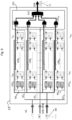
- FIG 6 it is shown a third embodiment 13" of the latch matrix according to the solution here described. Analogous or corresponding elements with respect to figure 4 and 5 are indicated by the same reference.
- This third embodiments 13" differs in that on top of a latch matrix corresponding to the latch matrix 13 of figure 4 , i.e. including latches in row and columns Loo... L WX , flip flops FFOo... FFOw are added at the beginning of the row representing each RAM location ML j .
- These flip flops FFO 0 ...FFO W are not used in functional mode, i.e., normal operation, but are added just to improve the capability of ATPG (Automatic Test Pattern Generation) to detect defects.
- ATPG Automatic Test Pattern Generation
- This solution can be used also with Mask capability, although it may be that when Mask capability is used coverage is already near to 100%, thus it is not necessary while the embodiment results less area efficient in case of no mask capability with respect to the embodiment of figure 5 .
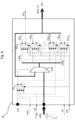
- figure 8 it is shown the FF output sampling logic 14, which is configured to decouple the outside output device logic with respect to the internal one.
- the Latch Data Bits signal LDB is sent to an input of a two inputs multiplexer 141, which at the other input receives as feedback from the output an output bus QQ[X...0] which is the memory output and output of the block 14.
- the multiplexer 141 receives as selection signal the output of a chip select flip flop FF CS , which at its data input receives the chip select signal CSS. In the example shown the multiplexer 141 selects the Latch Data Bits signal LDB if the selection signal from chip select flip flop FF CS is logic one.
- the bit 0... X of the Latch Data Bits signal LDB are sent to the data inputs of respective output sampling flip flops FFUo....FFUx which receive on their clock input CK the clock CLK.
- the output bus QQ[X... 0] is the memory output and is directly connected to the outputs Q of the output sampling flip flops FFUo....FFUx.
- the content of these output sampling flip flops FFUo....FFUx is updated on the clock CLK falling edge only when the sampled Chip_selection signals (in the chip sel flip flop FFCS) is active, i.e., logic value one as indicated, while maintain the status when not active, by selecting the output bus QQ[X... 0] fed back at the input of the multiplexer 141, in this example the value of the selections signal is logic zero.
- a Random Access Memory comprising an array 13, 13', 13" of storage elements arranged in rows and columns, the rows of storage elements identifying respective memory locations, wherein said array of storage elements comprises an array of delay type latches L 00 ...L WX , receiving at their data input, D, bits of the data to be stored, i.e., sampled data bus, SDB, and at their clock input, CK, a gated clock signal GC j ) corresponding to the memory location ML j to which they belong.
- variant embodiments may envisage that a column in said array of D type latches L 00 ...L WX comprise D scan ready flip flops in place of D type latches or a column of D flip flops is added to said array of D type latches L 10 ...L WX .
- the outputs of the latches Loo... L WX of an address location ML j are supplied to a data selector block 131 selecting latch Data Bits LDB corresponding to the address bits bus signal SAB, i.e. address the signal being currently asserted.
- the random access memory 10 comprise a clock input logic 12 configured to provide respective gated clocks GC j for each memory location ML j in the array of D type latches L 00 ...L WX said clock input logic 12 comprising
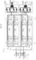
- figure 9 it is shown a second embodiment of the solution here described with dual port architecture RAM memory, indicated as whole with the reference number 20.
- the Dual Port RAM is an extension of the Single Port RAM, therefore in general only the differences vs the Single Port RAM 10 will be described in detail here below.
- the Dual Port RAM differs from the Single-Port RAM since read and write operations can be performed concurrently on the Dual Port RAM with the restriction that they cannot access the same address at the same time, while these operations, read and write, are mutually exclusive in the Single Port RAM (with the exception of writethrough feature in which the written data is transferred on the output, but this is not a "real" read operation since the write enable signal is in write mode).
- the Dual port RAM 20 receives input boundary signals a part of which corresponds basically to those received at the RAM 10, i.e. a write address bus signal WAD[0...Y] is received corresponding to the address bus AD[0...Y], a write data bus WB[0...X], a mask bus MB[0...X], a write clock signal CLKW, which performs a function analogous to signal CLK of the RAM 10 when operating as write clock (CLK it is as well as read clock since it clocks the flip-flops output sampling logic 14), a write enable signal WES, a write scan in signal WSIS, analogous to signals SIS in RAM 10, a scan enable signal SES, a reset signal RST.
- a write address bus signal WAD[0...Y] is received corresponding to the address bus AD[0...Y]
- a write data bus WB[0...X] a mask bus MB[0...X]
- CLKW write clock signal
- WES write enable signal
- WSIS write scan in signal WSIS
- the input boundary however further includes a set of read signals, i.e. a read address bus signal RAD[0...Y], i.e. a bus of Y+1 bits containing the read addresses, a read enable signal RES, enabling reading operations, a read clock signal CLKR clocking read operations, a read Scan In signal RSIS to implement the ATPG scan chain for read operations.
- a set of read signals i.e. a read address bus signal RAD[0...Y], i.e. a bus of Y+1 bits containing the read addresses
- a read enable signal RES enabling reading operations
- a read clock signal CLKR clocking read operations enabling reading operations
- RSIS read Scan In signal
- the Dual Port RAM 20 includes in the first place splitting the input sampling logic, i.e. includes a write input sampling logic 21w and a read sampling input sampling logic 21r, which respectively manage the control logic for Writing and Reading operation in a separate manner.
- write input sampling logic 21w corresponds to the input sampling logic 11, which is also for writing, i.e. it has the same architecture, components, and input and output signals, although here some are labelled as 'write' signals, e.g. write clock signal CLKW and write address WAD. It is underlined that in this case there is a difference between the write input sampling logic 21w and the input sampling logic 11, since chip select signal CSS is no longer available.
- the first test flip flop FFT1 receives the Write Enable signal WES signal directly (i.e., no AND 111) outputting a Sampled Write Enable signal SWES which is simply a resampling the signal WES.
- FIG 11 it is the shown the read input sampling logic 21r which receives the read address bus signal RAD [Y....0], the read clock CLKR, the read Scan In Signal RSIS, the Read enable signal RES.
- the block 21r comprises a row of address resampling delay flip flops FFR 0 ...FFR Y , all scan ready flip flops also in this case, receiving the read address bus signal RAD[Y....0], each flip-flop receiving a bit of the read address bus signal RAD[Y....0] and resampling it with the read clock signal CLKR to produce respective sampled read address bits SRAB as output of block 21r.
- Another output of block 21r is a sampled read enable SRES, sampled with the read clock signal CLKR in a further scan ready flip flop FFRE, which samples the Read Enable signal RES.
- the reset signal RST is supplied to all the reset input of the flip flops, while the Scan In read Signal RSIS is brought to the TI input of the first flip FFR0, while its output SO is coupled to the TI input of the following flip flop, and so on, this being exemplary of a possible way according to which the flip flops are cascaded with respect to the scan in signal RSIS, i.e. a possible implementation of a scan daisy chain, although other implementations are possible.
- the last flip-flop of the chain is the further scan ready flip flop FFRE, which receives the output SO of the last address resampling delay flip flop FFR Y and outputs the Scan out signal RSOS from its output SO.
- the clock input logic 22 which has the same architecture of the clock input logic 12, used in the Single port RAM 10, only receives as clock the write clock signal CLKW, while receives instead of the Sampled Add bits SAB the Sampled Write Add bits SWAB, although both in RAM 10 and 20 these signals refer to write operations.
- the signals besides the write label, correspond to the signals CLK and SAB of Figure 3 .
- the other signals and components in the block 22 are indicated by the same references, as they are obtained from signals which are analogous to that of Figure 3 , but are used only in write mode, in particular the gated clocks GC at the output.
- the Sampled Write Enable signal SWES is a sampled version of the Write Enable signal WES in this case.
- FIG 13 it shown the latched matrix 23, which is shown, with respect to the single matrix 13 as receiving, in addition to gated clock signals GC, Sampled Write Add bits SWAB (in particular, which replace Address bits SAB for the write function in this embodiment), Sampled Data bits SDB and Masked Data bits MDB, regarding the write mode. Also, Sample read address bits, which are used in the read mode, are indicated with SRAB.
- the latched matrix 23 includes a matrix of latches corresponding to that of the matrix 13, i.e., a matrix of latches in row and columns L 00 ...L WX coupled to a read data selector 131r, like the selector 131 in the matrix 13, for the read operations, which provides as output X+1 latch read data bits LRDB (corresponding to latch data bits LDB in Figure 4 ).
- a further optional write data selector 131w is provided for the masking capability, this meaning that is optional if no masking is used, which provides as output X+1 Latch Write Data Bits LWDB.
- write data selector blocks 131w which is optional, receives the Write Address Bus signal SWAB input, in particular as the input of the AND gates 132, described in Figure 4 , receiving at the other input of the AND gates 132 the content of the corresponding memory locations, the other read data selector blocks 131r receives instead the read address bus signal SRAB in particular as the input of the AND gates 132, described in Figure 4 , receiving at the other input of the AND gates 132 the content of the corresponding memory locations.
- FIG 14 it is shown the masking block 25 which correspond to the block 15 shown in figure 7 .
- the block 25 receives as input, fed back from the output of the matrix 23, the latch write data bits LWDB, outputted by the optional data selector 131w, then also receives the same single port input signals, SDB, SMB, SES, RST, while the clock signal fed to the block masking 25 is of course the write clock signal CKLW.
- the masked data bits MDB are output.
- FIG 15 it is shown the output sampling logic 24, which corresponds to the block 14 of figure 8 , the only difference with respect to signals, being that receives, instead of the latch data bit LDB, the latch read data bit LRDB as input.
- the clock signal received by the block 24 is the read clock signal CLKR.
- sampled scan enable SES and scan in signal RSIS are also provided, as well as the reset signal RST.
- the read operation is controlled directly by the Sampled Read Enable signal SRES coming from the FF input Read sampling logic 21r, which represent here the selection signal of the multiplexer 141 directly, without being combined with the chip select signal CSS in a specific flip flop like in block 14, i.e.
- the logic 24 does not comprise the flip flop FF CS . These changes are required since this block is active only when Read mode is performed. Besides this difference the architecture is the same of block 14, finally outputting the output signal QQ, which contains the read data, sampled with the read clock CLKR.
- the Single Port RAM 10 or Dual Port RAM 20 may operate with rising edges instead that with falling edges.
- the optional Mask data Management 15 changes instead sampling from rising edge to falling edge. It is specified to this regard that for clock CLK in the memory 10 (or 20) sampled on the falling edge or respectively rising edge, is intended the sampling performed on Flip-Flop Input sampling logic 11, and Flip-Flop Output sampling logic 14.
- the modifications affect latches LLoo... LL WX of the matrix.
- the latches transparent on positive, or high, clock (identified with gated clock input G of the latches in figure 4 ) need to be replaced with latches transparent when the clock signal at the gated clock input G is low, i.e. they are the same type of the latches FFC in Figure 3 which receive at its clock input GN the negated of the clock CLK.
- the gated clock signals GCo... GCw clocks need to be different.
- the clock gate control logic 12 requires instead some additional modification, in addition to the change of the edge of the clock, as indicated in figure 16 , which show a variant clock gate control logic 12' operating with rising edge of the clock CLK.
- the modifications to the clock gate control logic 12' shown in Figure 16 in this case are of two types: the edge of the boundary signals, which for input signals SAB/SWE/STM has sampling on the rising edge as better detailed below, and the one related to the clock gating cells indicated as 123 in figure 3 .
- the clock gate control logic 12' uses clock gating cells 123' where:
- clock gating cells 123 which are able to manage propagate positive pulse, i.e. at high logic level, for sampling on the falling edge, are changed, for sampling on the rising edge, to clock gating cells 123' able to manage the propagation of negative pulse, i.e. at low logic level, as mentioned above.
- the implementation of the clock gating cell 123' is one of many possible, it is relevant that the clock gating cell 123' is configured to propagate negative pulses.
- the signal of reset RST can be also act as a set for the latches FFC j , i.e. sent to its SET input. In figure 16 this is shown only for latch FFC W-1 , for simplicity. This might prevent X propagation at the begin if the clock CLK has off-state low.
- figure 16 shows thus the edge clock on address signal SAB, sampled write enable signal SWE and STM signals with the arrow on the rising edge of the clock, thus gated clock signals GC happen to be at low logic level only when the clock CLK is at low logic level also because there is an OR (125 which requires both the input low) to have output low.
- the solution described thus allows advantageously to obtain an RTL Scalable solution on functionality (mask or no-mask writing capability) and on target Fault Coverage.
- the solution described can obtain till 50% area reduction with respect to a full Flip-Flop matrix implementation. Depending on cut size, it is also smaller than using RAM memories with a BIST. Automotive grade coverage may be obtained for both Stuck-at (>99%) and Transition fault (>>90%).
- LBIST capable ("X" propagation prevented thanks to shadow architecture, e.g., the OR 122 introduced between Sampled Test Mode STM and Scan Enable signal SES, a logic gate which operates in combination with the one hot address decoder).
- a one clock cycle latency may be obtained (valid on reading and both mask or no-mask writing capability)
- Clock edge can be reverted (Input/output sampling on rising edge and latch on low clock).
- the solution can be applied both to single and Dual-Port RAM.
Landscapes
- Engineering & Computer Science (AREA)
- Theoretical Computer Science (AREA)
- Microelectronics & Electronic Packaging (AREA)
- Computer Hardware Design (AREA)
- Physics & Mathematics (AREA)
- General Engineering & Computer Science (AREA)
- General Physics & Mathematics (AREA)
- Tests Of Electronic Circuits (AREA)
Applications Claiming Priority (1)
| Application Number | Priority Date | Filing Date | Title |
|---|---|---|---|
| IT102022000007967A IT202200007967A1 (it) | 2022-04-22 | 2022-04-22 | Memoria ad accesso casuale e corrispondente metodo di gestione di una memoria ad accesso casuale |
Publications (1)
| Publication Number | Publication Date |
|---|---|
| EP4266313A1 true EP4266313A1 (de) | 2023-10-25 |
Family
ID=82308396
Family Applications (1)
| Application Number | Title | Priority Date | Filing Date |
|---|---|---|---|
| EP23163536.8A Pending EP4266313A1 (de) | 2022-04-22 | 2023-03-22 | Direktzugriffsspeicher und zugehöriges verfahren zur verwaltung eines direktzugriffsspeichers |
Country Status (3)
| Country | Link |
|---|---|
| US (1) | US12073897B2 (de) |
| EP (1) | EP4266313A1 (de) |
| IT (1) | IT202200007967A1 (de) |
Families Citing this family (2)
| Publication number | Priority date | Publication date | Assignee | Title |
|---|---|---|---|---|
| US20240404613A1 (en) * | 2022-04-22 | 2024-12-05 | Stmicroelectronics S.R.L. | Random access memory and corresponding method for managing a random access memory |
| TWI887983B (zh) * | 2024-01-26 | 2025-06-21 | 瑞昱半導體股份有限公司 | 具有記憶體輸出遮蔽機制的記憶體裝置 |
Citations (1)
| Publication number | Priority date | Publication date | Assignee | Title |
|---|---|---|---|---|
| US20200059223A1 (en) * | 2018-08-15 | 2020-02-20 | Taiwan Semiconductor Manufacturing Company, Ltd. | Flip flop standard cell |
Family Cites Families (2)
| Publication number | Priority date | Publication date | Assignee | Title |
|---|---|---|---|---|
| US9799379B2 (en) * | 2012-07-20 | 2017-10-24 | Nxp Usa, Inc. | Hold time aware register file module and method therefor |
| US11443823B2 (en) * | 2020-10-29 | 2022-09-13 | SambaNova Systems, Inc. | Method and circuit for scan dump of latch array |
-
2022
- 2022-04-22 IT IT102022000007967A patent/IT202200007967A1/it unknown
-
2023
- 2023-03-22 EP EP23163536.8A patent/EP4266313A1/de active Pending
- 2023-04-13 US US18/300,091 patent/US12073897B2/en active Active
Patent Citations (1)
| Publication number | Priority date | Publication date | Assignee | Title |
|---|---|---|---|---|
| US20200059223A1 (en) * | 2018-08-15 | 2020-02-20 | Taiwan Semiconductor Manufacturing Company, Ltd. | Flip flop standard cell |
Non-Patent Citations (1)
| Title |
|---|
| TEMAN ADAM ET AL: "Controlled placement of standard cell memory arrays for high density and low power in 28nm FD-SOI", THE 20TH ASIA AND SOUTH PACIFIC DESIGN AUTOMATION CONFERENCE, IEEE, 19 January 2015 (2015-01-19), pages 81 - 86, XP032745341, DOI: 10.1109/ASPDAC.2015.7058985 * |
Also Published As
| Publication number | Publication date |
|---|---|
| US12073897B2 (en) | 2024-08-27 |
| US20230343405A1 (en) | 2023-10-26 |
| IT202200007967A1 (it) | 2023-10-22 |
Similar Documents
| Publication | Publication Date | Title |
|---|---|---|
| US7543207B2 (en) | Full scan solution for latched-based design | |
| US8028209B2 (en) | Scalable scan system for system-on-chip design | |
| EP4266313A1 (de) | Direktzugriffsspeicher und zugehöriges verfahren zur verwaltung eines direktzugriffsspeichers | |
| KR100303618B1 (ko) | 셀프-타임식메모리어레이를갖는완전테스트가능한칩 | |
| US5781560A (en) | System testing device and method using JTAG circuit for testing high-package density printed circuit boards | |
| US20100037109A1 (en) | Method for at-speed testing of memory interface using scan | |
| US7533309B2 (en) | Testing memories using algorithm selection | |
| US8780648B2 (en) | Latch based memory device | |
| KR20060043690A (ko) | 테스트 회로, 그 테스트 회로를 내장한 반도체집적회로장치및 그 테스트 방법 | |
| US20240249791A1 (en) | Single "a" latch with an array of "b" latches | |
| US6567943B1 (en) | D flip-flop structure with flush path for high-speed boundary scan applications | |
| CA2286473A1 (en) | Fault insertion method, boundary scan cells, and integrated circuit for use therewith | |
| CN116935908A (zh) | 随机存取存储器以及用于管理随机存取存储器的对应方法 | |
| US7779316B2 (en) | Method of testing memory array at operational speed using scan | |
| US20080256405A1 (en) | Compilable memory structure and test methodology for both asic and foundry test environments | |
| US20240404613A1 (en) | Random access memory and corresponding method for managing a random access memory | |
| US7925937B2 (en) | Apparatus for testing embedded memory read paths | |
| Wielage et al. | Design and DfT of a high-speed area-efficient embedded asynchronous FIFO | |
| US6341092B1 (en) | Designing memory for testability to support scan capability in an asic design | |
| Xu et al. | Achieving high transition delay fault coverage with partial DTSFF scan chains | |
| CN115701876B (zh) | 针对基于锁存器的存储器来减少面积的atpg测试方法 | |
| US20080059853A1 (en) | Semiconductor Integrated Circuit | |
| US11809740B1 (en) | Fast and flexible RAM reader and writer | |
| US20020075058A1 (en) | Apparatus for low-power, high performance, and cycle accurate test simulation | |
| CN120564813A (zh) | 一种sram的故障测试结构 |
Legal Events
| Date | Code | Title | Description |
|---|---|---|---|
| STAA | Information on the status of an ep patent application or granted ep patent |
Free format text: STATUS: THE APPLICATION HAS BEEN PUBLISHED |
|
| PUAI | Public reference made under article 153(3) epc to a published international application that has entered the european phase |
Free format text: ORIGINAL CODE: 0009012 |
|
| AK | Designated contracting states |
Kind code of ref document: A1 Designated state(s): AL AT BE BG CH CY CZ DE DK EE ES FI FR GB GR HR HU IE IS IT LI LT LU LV MC ME MK MT NL NO PL PT RO RS SE SI SK SM TR |
|
| STAA | Information on the status of an ep patent application or granted ep patent |
Free format text: STATUS: REQUEST FOR EXAMINATION WAS MADE |
|
| 17P | Request for examination filed |
Effective date: 20240325 |
|
| RBV | Designated contracting states (corrected) |
Designated state(s): AL AT BE BG CH CY CZ DE DK EE ES FI FR GB GR HR HU IE IS IT LI LT LU LV MC ME MK MT NL NO PL PT RO RS SE SI SK SM TR |