EP4264752B1 - Dispositif d'amplification d'un faisceau laser - Google Patents
Dispositif d'amplification d'un faisceau laser Download PDFInfo
- Publication number
- EP4264752B1 EP4264752B1 EP21839957.4A EP21839957A EP4264752B1 EP 4264752 B1 EP4264752 B1 EP 4264752B1 EP 21839957 A EP21839957 A EP 21839957A EP 4264752 B1 EP4264752 B1 EP 4264752B1
- Authority
- EP
- European Patent Office
- Prior art keywords
- laser medium
- active laser
- useful
- return unit
- front face
- Prior art date
- Legal status (The legal status is an assumption and is not a legal conclusion. Google has not performed a legal analysis and makes no representation as to the accuracy of the status listed.)
- Active
Links
Images



Classifications
-
- H—ELECTRICITY
- H01—ELECTRIC ELEMENTS
- H01S—DEVICES USING THE PROCESS OF LIGHT AMPLIFICATION BY STIMULATED EMISSION OF RADIATION [LASER] TO AMPLIFY OR GENERATE LIGHT; DEVICES USING STIMULATED EMISSION OF ELECTROMAGNETIC RADIATION IN WAVE RANGES OTHER THAN OPTICAL
- H01S3/00—Lasers, i.e. devices using stimulated emission of electromagnetic radiation in the infrared, visible or ultraviolet wave range
- H01S3/005—Optical devices external to the laser cavity, specially adapted for lasers, e.g. for homogenisation of the beam or for manipulating laser pulses, e.g. pulse shaping
- H01S3/0071—Beam steering, e.g. whereby a mirror outside the cavity is present to change the beam direction
-
- H—ELECTRICITY
- H01—ELECTRIC ELEMENTS
- H01S—DEVICES USING THE PROCESS OF LIGHT AMPLIFICATION BY STIMULATED EMISSION OF RADIATION [LASER] TO AMPLIFY OR GENERATE LIGHT; DEVICES USING STIMULATED EMISSION OF ELECTROMAGNETIC RADIATION IN WAVE RANGES OTHER THAN OPTICAL
- H01S3/00—Lasers, i.e. devices using stimulated emission of electromagnetic radiation in the infrared, visible or ultraviolet wave range
- H01S3/005—Optical devices external to the laser cavity, specially adapted for lasers, e.g. for homogenisation of the beam or for manipulating laser pulses, e.g. pulse shaping
-
- H—ELECTRICITY
- H01—ELECTRIC ELEMENTS
- H01S—DEVICES USING THE PROCESS OF LIGHT AMPLIFICATION BY STIMULATED EMISSION OF RADIATION [LASER] TO AMPLIFY OR GENERATE LIGHT; DEVICES USING STIMULATED EMISSION OF ELECTROMAGNETIC RADIATION IN WAVE RANGES OTHER THAN OPTICAL
- H01S3/00—Lasers, i.e. devices using stimulated emission of electromagnetic radiation in the infrared, visible or ultraviolet wave range
- H01S3/005—Optical devices external to the laser cavity, specially adapted for lasers, e.g. for homogenisation of the beam or for manipulating laser pulses, e.g. pulse shaping
- H01S3/0064—Anti-reflection devices, e.g. optical isolaters
-
- H—ELECTRICITY
- H01—ELECTRIC ELEMENTS
- H01S—DEVICES USING THE PROCESS OF LIGHT AMPLIFICATION BY STIMULATED EMISSION OF RADIATION [LASER] TO AMPLIFY OR GENERATE LIGHT; DEVICES USING STIMULATED EMISSION OF ELECTROMAGNETIC RADIATION IN WAVE RANGES OTHER THAN OPTICAL
- H01S3/00—Lasers, i.e. devices using stimulated emission of electromagnetic radiation in the infrared, visible or ultraviolet wave range
- H01S3/02—Constructional details
- H01S3/025—Constructional details of solid state lasers, e.g. housings or mountings
-
- H—ELECTRICITY
- H01—ELECTRIC ELEMENTS
- H01S—DEVICES USING THE PROCESS OF LIGHT AMPLIFICATION BY STIMULATED EMISSION OF RADIATION [LASER] TO AMPLIFY OR GENERATE LIGHT; DEVICES USING STIMULATED EMISSION OF ELECTROMAGNETIC RADIATION IN WAVE RANGES OTHER THAN OPTICAL
- H01S3/00—Lasers, i.e. devices using stimulated emission of electromagnetic radiation in the infrared, visible or ultraviolet wave range
- H01S3/05—Construction or shape of optical resonators; Accommodation of active medium therein; Shape of active medium
- H01S3/06—Construction or shape of active medium
- H01S3/0602—Crystal lasers or glass lasers
- H01S3/0606—Crystal lasers or glass lasers with polygonal cross-section, e.g. slab, prism
-
- H—ELECTRICITY
- H01—ELECTRIC ELEMENTS
- H01S—DEVICES USING THE PROCESS OF LIGHT AMPLIFICATION BY STIMULATED EMISSION OF RADIATION [LASER] TO AMPLIFY OR GENERATE LIGHT; DEVICES USING STIMULATED EMISSION OF ELECTROMAGNETIC RADIATION IN WAVE RANGES OTHER THAN OPTICAL
- H01S3/00—Lasers, i.e. devices using stimulated emission of electromagnetic radiation in the infrared, visible or ultraviolet wave range
- H01S3/05—Construction or shape of optical resonators; Accommodation of active medium therein; Shape of active medium
- H01S3/06—Construction or shape of active medium
- H01S3/0619—Coatings, e.g. AR, HR, passivation layer
- H01S3/0621—Coatings on the end-faces, e.g. input/output surfaces of the laser light
-
- H—ELECTRICITY
- H01—ELECTRIC ELEMENTS
- H01S—DEVICES USING THE PROCESS OF LIGHT AMPLIFICATION BY STIMULATED EMISSION OF RADIATION [LASER] TO AMPLIFY OR GENERATE LIGHT; DEVICES USING STIMULATED EMISSION OF ELECTROMAGNETIC RADIATION IN WAVE RANGES OTHER THAN OPTICAL
- H01S3/00—Lasers, i.e. devices using stimulated emission of electromagnetic radiation in the infrared, visible or ultraviolet wave range
- H01S3/05—Construction or shape of optical resonators; Accommodation of active medium therein; Shape of active medium
- H01S3/06—Construction or shape of active medium
- H01S3/0619—Coatings, e.g. AR, HR, passivation layer
- H01S3/0621—Coatings on the end-faces, e.g. input/output surfaces of the laser light
- H01S3/0623—Antireflective [AR]
-
- H—ELECTRICITY
- H01—ELECTRIC ELEMENTS
- H01S—DEVICES USING THE PROCESS OF LIGHT AMPLIFICATION BY STIMULATED EMISSION OF RADIATION [LASER] TO AMPLIFY OR GENERATE LIGHT; DEVICES USING STIMULATED EMISSION OF ELECTROMAGNETIC RADIATION IN WAVE RANGES OTHER THAN OPTICAL
- H01S3/00—Lasers, i.e. devices using stimulated emission of electromagnetic radiation in the infrared, visible or ultraviolet wave range
- H01S3/23—Arrangements of two or more lasers not provided for in groups H01S3/02 - H01S3/22, e.g. tandem arrangements of separate active media
- H01S3/2308—Amplifier arrangements, e.g. MOPA
- H01S3/2325—Multi-pass amplifiers, e.g. regenerative amplifiers
-
- H—ELECTRICITY
- H01—ELECTRIC ELEMENTS
- H01S—DEVICES USING THE PROCESS OF LIGHT AMPLIFICATION BY STIMULATED EMISSION OF RADIATION [LASER] TO AMPLIFY OR GENERATE LIGHT; DEVICES USING STIMULATED EMISSION OF ELECTROMAGNETIC RADIATION IN WAVE RANGES OTHER THAN OPTICAL
- H01S3/00—Lasers, i.e. devices using stimulated emission of electromagnetic radiation in the infrared, visible or ultraviolet wave range
- H01S3/23—Arrangements of two or more lasers not provided for in groups H01S3/02 - H01S3/22, e.g. tandem arrangements of separate active media
- H01S3/2308—Amplifier arrangements, e.g. MOPA
- H01S3/2325—Multi-pass amplifiers, e.g. regenerative amplifiers
- H01S3/2333—Double-pass amplifiers
-
- H—ELECTRICITY
- H01—ELECTRIC ELEMENTS
- H01S—DEVICES USING THE PROCESS OF LIGHT AMPLIFICATION BY STIMULATED EMISSION OF RADIATION [LASER] TO AMPLIFY OR GENERATE LIGHT; DEVICES USING STIMULATED EMISSION OF ELECTROMAGNETIC RADIATION IN WAVE RANGES OTHER THAN OPTICAL
- H01S3/00—Lasers, i.e. devices using stimulated emission of electromagnetic radiation in the infrared, visible or ultraviolet wave range
- H01S3/23—Arrangements of two or more lasers not provided for in groups H01S3/02 - H01S3/22, e.g. tandem arrangements of separate active media
- H01S3/2308—Amplifier arrangements, e.g. MOPA
- H01S3/2325—Multi-pass amplifiers, e.g. regenerative amplifiers
- H01S3/2341—Four pass amplifiers
-
- H—ELECTRICITY
- H01—ELECTRIC ELEMENTS
- H01S—DEVICES USING THE PROCESS OF LIGHT AMPLIFICATION BY STIMULATED EMISSION OF RADIATION [LASER] TO AMPLIFY OR GENERATE LIGHT; DEVICES USING STIMULATED EMISSION OF ELECTROMAGNETIC RADIATION IN WAVE RANGES OTHER THAN OPTICAL
- H01S2301/00—Functional characteristics
- H01S2301/02—ASE (amplified spontaneous emission), noise; Reduction thereof
Definitions
- the present invention relates to a device for amplifying a multi-wavelength laser beam.
- the field of the invention is that of solid-state laser sources for scientific, industrial, medical and military applications. More specifically, it is advantageously used for amplifying medium materials (such as a crystal) which have a relatively small thickness compared to their aperture along the propagation axis of the laser beam, typically less than 1:3.
- medium materials such as a crystal
- the thick disk solution is well suited for some amplifying media such as amorphous materials (like glasses), transparent ceramics or crystals like Ti:Sa (short for Titanium:Sapphire). It allows access to high energy levels, high average powers, and short pulse durations thanks to the broad amplification spectrum of the material.
- the amplifying medium e.g. a crystal
- the cooling is then achieved by means of a fluid, liquid or gas, or a solid.
- Such cooling from the rear face increases the heat exchange surface. It also generates a thermal gradient in the direction of propagation of the laser in the crystal, and also achieves high thermal extraction.
- the index variations related to temperature variations in the crystal are gradients that are predominantly oriented in the same direction as the direction of propagation of the laser beam.
- back-cooled laser amplification devices induce geometric folding of the beam due to the reflective back face of the crystal.
- the output face of the crystal is then the same as the input face, which implies that the parasitic pulses (due to parasitic reflections on the front face) are found before the main pulse, consequently degrading the temporal contrast of the pulse.
- the temporal contrast is defined by the ratio between the intensity of the main pulse and the foot of the pulse and/or any parasitic pulses.
- this angle produces a prismatic effect which is compensated by a compensation prism positioned on the beam path, as described in EP 2 915 226 B.
- a compensation prism positioned on the beam path, as described in EP 2 915 226 B.
- a propagation direction z is defined, represented in the figures by a z axis and corresponding to the propagation direction of the laser beam.
- a first transverse direction is defined, perpendicular to the propagation direction, and represented in the figures by an x axis, such that the plane (xOz) corresponds to a top view of the amplification device 10.
- a second transverse direction y perpendicular to the propagation direction z and to the first transverse direction x.
- the second transverse direction y is represented in the figures by a y axis and is such that the plane (yOz) corresponds to a side view of the amplification device 10.
- chromatic spatial dispersion is understood to mean the angular dispersion of a beam due to variations in the deviation angle as a function of the wavelengths in a diopter.
- chromatic lateral dispersion is understood to mean the broadening of the diameter of a beam as a function of the wavelengths (pupil shift) following passage through two diopters whose interfaces are parallel (plates with parallel faces).
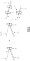
- a first embodiment of an amplification device 10 is illustrated by the figure 1 .
- the amplification device 10 is configured to amplify a laser beam, in particular a multi-wavelength pulsed laser beam.
- the beam to be amplified is, for example, an infrared beam.
- the beam to be amplified has, for example, an average power greater than 10 Watts (W).
- the amplification device 10 comprises an amplifying medium M and a first optical return unit 18.
- the medium M is a solid medium.
- the medium M is, for example, a crystal such as Titanium-doped sapphire, or Yb:YAG, Yb:CaF2 or a polymer, a ceramic or a glass or any other material in the solid state.
- the medium M has a refractive index n.
- n refractive index
- v is the constringency of the amplifying medium M. This aims to preserve the multi-wavelength character of the beam F S at the output of the amplification device 10.
- the medium M has at least two flat faces including a front face 20 suitable for receiving the beam to be amplified each time said beam passes through the amplifying medium M and a reflective rear face 22.
- the front face 20 is inclined relative to the rear face 22 by a non-zero inclination ⁇ (angle).
- ⁇ ' denotes the projection of the inclination ⁇ onto the plane (xOz)
- ⁇ " the projection of the inclination ⁇ onto the plane (yOz).
- the amplifying medium M is a disk whose faces (front 20 and rear 22) are inscribed in a right prism with a triangular or trapezoidal base, called base 24.
- the base 24 of the prism, and therefore the inclination ⁇ is entirely contained in a plane perpendicular to, on the one hand, a plane P 22 containing the rear face 22, and on the other hand, to a plane perpendicular to the plane (yOz).
- the front face 20 of the amplifying medium M is suitable for receiving the beam to be amplified at each passage of said beam in the amplifying medium M and for, on the one hand, reflecting a parasitic beam (direct reflection) and, on the other hand, refracting a useful beam after such a beam has been reflected by the rear face 22.
- the beam received on the front face 20 during the first passage is called the incident beam F I .
- the beam reflected by the rear face 22 and refracted by the front face 20 during the nth passage is called the nth useful beam F Un .
- the useful beam at the output of the amplifying medium M during the last passage is also called the output beam F S .
- the beam directly reflected by the front face 20 from the beam to be amplified during the nth passage is called the nth parasitic beam F Pn .
- the front face 20 is anti-reflective treated.
- the rear face 22 of the amplifying medium M is capable of reflecting, at each passage, the beam to be amplified, after its passage through the front face 20 of the amplifying medium M, to form the corresponding useful beam.
- the rear face 22 is suitable for being cooled by a cooling device, which is, for example, included in the amplification device 10.
- the cooling is shown in the figure 1 by an arrow attached to the rear face 22.
- the first optical return unit 18 is arranged on the path of the first useful beam F U1 .
- the first optical return unit 18 is configured so as to return the first useful beam F U1 to the front face 20 for a second passage in the amplifying medium M so that the sub-beams of each length wave, forming the second useful beam F U2 , are parallel to each other at the end of the second pass.
- On the figure 1 only two sub-beams are shown so as not to overload the figure.
- the first optical return unit 18 thus makes it possible to compensate for the chromatic spatial dispersion induced by the prismatic effect resulting from the inclination ⁇ between the front face 20 and the rear face 22 of the amplifying medium M.
- the first optical return unit 18 is configured so that the second useful beam F U2 is equivalent in terms of chromatic spatial dispersion to the beam which would have been obtained at the output of a plate with flat and parallel faces L1 from an incident beam arriving on the front face of said plate with an angle of incidence equal to the angle of incidence ⁇ of the incident beam F I on the amplifying medium M.
- the first optical return unit 18 comprises two mirrors M1, M2 oriented so that the path of the first useful beam F U1 between the amplifying medium M and the first mirror M1 is symmetrical, with respect to a plane of symmetry P H , to the path of the first useful beam F U1 between the second mirror M2 and the amplifying medium M.
- the plane of symmetry P H is a plane perpendicular, on the one hand, to a plane P 24 containing the base 24 of the amplifying medium M and, on the other hand, to a plane P 22 containing the rear face 22.
- the plane of symmetry P H is a plane perpendicular to the plane (xOz) (plane of the sheet on the figure 1 ) and perpendicular to a plane P 22 containing the back face 22, and the image is flipped in the x direction.
- the first optical return unit 18 does not include a prism.
- the first optical return unit 18 is arranged outside the path of the first parasitic beam F P1 .
- the beam (pulse) to be amplified F I of diameter ⁇ arrives on the front face 20 of the amplifying medium M with an angle of incidence ⁇ which is decomposed into an angle ⁇ x in the plane (xOz) and an angle ⁇ y in the plane (yOz).
- the useful beam (main pulse) is reflected by the rear face 22, the parasitic beam F P1 by the front face 20.
- the parasitic beam also called pulses parasites, is deflected on this front face 20 by an angle 2 ⁇ x in the plane (xOz) and 2 ⁇ y in the plane (yOz).
- the angle ⁇ formed by the faces 20 and 22 produces a prismatic effect.
- the wavelengths of the first useful beam F U1 are angularly separated.
- the first optical return unit 18 arranged after the separation of the first useful beam F u1 and the first parasitic beam F P1 , on the path of the first useful beam F U1 makes it possible to correct the chromatic spatial dispersion.
- the spectral components of the second useful beam F u2 form a spot of diameter ⁇ + ⁇ .
- ⁇ includes the increase in diameter introduced by the divergence of the beam during the first passage in the amplifying medium M, then that introduced by the divergence of the beam between its exit from the amplifying medium M and its second entry into the amplifying medium M.
- the same diameter ⁇ + ⁇ is found after the second passage in the amplifying medium M.
- the broadening ⁇ of the diameter of the second useful beam F u2 must be small compared to ⁇ . This is the case when n ⁇ n ⁇ 1 ⁇ .
- the amplification device 10 makes it possible to compensate for the chromatic spatial dispersion induced by the inclination ⁇ of the amplifying medium M without, however, introducing additional losses.
- the compensation is carried out by an additional passage in the amplifying medium M itself which does not introduce losses, but on the contrary more gain.
- the amplification device 10 according to the first embodiment therefore makes it possible to minimize optical losses while remaining satisfactory in terms of cooling, gain and temporal contrast.
- the amplification device 10 comprises a second optical return unit 30 capable of returning the second useful beam F U2 into the amplifying medium M for at least a third, then a fourth pass so that the last useful beam at the output of the amplifying medium M, called the output beam F S , has a diameter substantially equal to the diameter ⁇ of the incident beam F I and that the sub-beams of each wavelength, forming said output beam F S , are parallel to each other.
- the optical assembly formed by the first optical return unit 18 and the second optical return unit 30 makes it possible to compensate for both the chromatic spatial dispersion and the chromatic lateral dispersion.
- the second optical return unit 30 is configured so that the output beam F S is equivalent in terms of diameter (chromatic lateral dispersion) and chromatic spatial dispersion to the beam that would have been obtained following the successive passage of an incident beam through a first, then a second plate with flat and parallel faces L1 and L2, the first plate L1 being oriented so that the incident beam arrives on the front face of the first plate with a first angle of incidence ⁇ 1 equal to the angle of incidence ⁇ of the incident beam on the amplifying medium M, the second plate L2 being oriented so as to receive the beam at the output of the first plate L1 with a second angle of incidence ⁇ 2 equal to the opposite of the first angle of incidence ⁇ 1 .
- the second optical return unit 30 is capable of returning the second useful beam F U2 into the amplifying medium M so that the total number of passages of the beam to be amplified in the amplifying medium M is a multiple of four.
- the second optical return unit is capable of returning the second useful beam F U2 into the amplifying medium M such that the total number of passages of the beam to be amplified in the amplifying medium M is a multiple of two and that the beam to be amplified makes an outward path and a return path, superimposed on the outward path, between the first entry of said beam into the amplifying medium M and the last exit of said beam from the amplifying medium M.
- this makes it possible to compensate for the chromatic lateral dispersion of the beam F S at the output of the amplification device 10.
- the beam to be amplified makes four passes through the amplifying medium M.
- the second optical return unit 30 comprises a mirror M AR (plane mirror) suitable for making the beam to be amplified make a round trip in the amplification device 10.
- the beam to be amplified already makes two passes via the first optical unit 18, the total number of passes in the amplifying medium M is four.
- the second optical return unit 30 comprises four mirrors M3, M4, M5 and M6.
- the mirrors M3 and M4 are suitable for returning the second useful beam F U2 into the amplifying medium M for a third passage through the amplifying medium M.
- the mirrors M5 and M6 are suitable for returning the third useful beam F U3 into the amplifying medium M for a fourth passage through the amplifying medium M.
- the total number of passages through the amplifying medium M is thus four.
- P H denotes a horizontal plane of symmetry for the mirrors M1, M2 of the amplification device 10 and Pv a vertical plane of symmetry for the mirrors M1, M2 relative to the mirrors M5, M6.
- the beam to be amplified enters through the quadrant 1) of the medium M, the second passage is made through the quadrant 2), the third passage through the quadrant 3), and the fourth passage through the quadrant 4).
- the second optical return unit 30 comprises at least one mirror.
- the second optical return unit 30 does not include a prism.
- the first return unit 18 and the second return unit 30 are arranged outside the path of each parasitic beam resulting from an odd passage in the amplifying medium M.
- the first parasitic beam F P1 and the third parasitic beam F P3 are not returned into the amplifying medium M and are, thus, eliminated.
- the amplification device 10 comprises, for example, an optical separation assembly 40 for separating the two beams.
- the optical separation assembly 40 comprises a polarizing cube 42 and a quarter-wave plate 44, as well as a mirror M0.
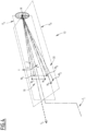
- the incident beam F I and the output beam F S are spatially offset (not superimposed).
- Such a configuration is notably illustrated in figure 4 .
- Such a configuration makes it possible to dispense with an optical assembly for separating the incident beam F I and the output beam F S .
- the second useful beam F U2 is returned, via the second optical unit 30, to the front face 20 of the amplifying medium M, for a third passage in said medium M.
- the third useful beam F U3 is in turn returned, via the second optical unit 30, to the front face 20 of the amplifying medium M, for a fourth passage in said medium M.
- the parasitic reflections F P2 , F P3 and F P4 have not been shown.
- the configuration of the second optical unit 30 relative to the first optical unit 18 and to the amplifying medium M thus makes it possible to compensate for the chromatic lateral dispersion of the amplified output beam of the amplification device 10.
- the parasitic beams generated during odd passages in the amplifying medium M are not returned into the amplifying medium M and are ejected.
- the parasitic beams generated during even passages in the amplifying medium M are also easily dissociable from the useful beam. Indeed, in the case of a two-dimensional assembly ( figure 3 ), the parasitic pulses generated during even passages take the same optical path as the useful pulses but are delayed compared to the main pulse. Such pulses will, therefore, be at the origin of a "post pulse" after the useful beam (pulse). As these parasitic pulses arrive after the useful beam, they do not reduce the contrast and it is easy to filter them. In the case of a three-dimensional assembly ( figure 4 ), the parasitic pulses generated during even passages take the same optical path as the useful pulses but in the opposite direction, and thus do not affect the contrast.
- the amplification device 10 makes it possible, in addition to the advantages of the first embodiment, to compensate for the lateral chromatic dispersion induced during the first two crossings of the amplifying medium M, and this without introducing additional losses.
- the compensation is carried out by additional passages in the amplifying medium M which thus introduce an amplification gain while remaining satisfactory in terms of cooling and temporal contrast.
- the examples of figures 3 And 4 illustrate only four passages in the amplifying medium M. Nevertheless, the second embodiment generalizes to a greater number of passages in the amplifying medium M with the condition that either this number is a multiple of four (a multiple of two but not of four would only amount to compensating for the chromatic spatial dispersion but not the chromatic lateral dispersion), or that this number is a multiple of two but that the beam to be amplified makes a round trip in the amplification device 10.
Landscapes
- Physics & Mathematics (AREA)
- Electromagnetism (AREA)
- Engineering & Computer Science (AREA)
- Plasma & Fusion (AREA)
- Optics & Photonics (AREA)
- Chemical & Material Sciences (AREA)
- Crystallography & Structural Chemistry (AREA)
- Lasers (AREA)
- Laser Surgery Devices (AREA)
Applications Claiming Priority (2)
| Application Number | Priority Date | Filing Date | Title |
|---|---|---|---|
| FR2013475A FR3118329B1 (fr) | 2020-12-17 | 2020-12-17 | Dispositif d’amplification d’un faisceau laser |
| PCT/EP2021/086116 WO2022129293A1 (fr) | 2020-12-17 | 2021-12-16 | Dispositif d'amplification d'un faisceau laser |
Publications (2)
| Publication Number | Publication Date |
|---|---|
| EP4264752A1 EP4264752A1 (fr) | 2023-10-25 |
| EP4264752B1 true EP4264752B1 (fr) | 2024-10-09 |
Family
ID=76034663
Family Applications (1)
| Application Number | Title | Priority Date | Filing Date |
|---|---|---|---|
| EP21839957.4A Active EP4264752B1 (fr) | 2020-12-17 | 2021-12-16 | Dispositif d'amplification d'un faisceau laser |
Country Status (12)
| Country | Link |
|---|---|
| US (1) | US20240055818A1 (lt) |
| EP (1) | EP4264752B1 (lt) |
| JP (1) | JP2023554480A (lt) |
| KR (1) | KR20230119143A (lt) |
| CN (1) | CN116648831A (lt) |
| CA (1) | CA3202454A1 (lt) |
| ES (1) | ES3002334T3 (lt) |
| FR (1) | FR3118329B1 (lt) |
| HU (1) | HUE069823T2 (lt) |
| IL (1) | IL303719B1 (lt) |
| LT (1) | LT4264752T (lt) |
| WO (1) | WO2022129293A1 (lt) |
Families Citing this family (1)
| Publication number | Priority date | Publication date | Assignee | Title |
|---|---|---|---|---|
| DE102023108777A1 (de) * | 2023-04-05 | 2024-10-10 | Deutsches Zentrum für Luft- und Raumfahrt e.V. | Lasersystem, Verfahren zur Erzeugung wenigstens eines geformten und verstärkten Laserstrahls mit einem Lasersystem sowie optisches System |
Citations (1)
| Publication number | Priority date | Publication date | Assignee | Title |
|---|---|---|---|---|
| EP2915226B1 (fr) * | 2012-10-31 | 2016-10-26 | Thales | Dispositif d'amplification d'un laser impulsionnel a contraste temporel ameliore |
Family Cites Families (15)
| Publication number | Priority date | Publication date | Assignee | Title |
|---|---|---|---|---|
| US5172263A (en) * | 1991-05-10 | 1992-12-15 | Amoco Corporation | Multi-pass laser amplifier system |
| US20010021215A1 (en) * | 1999-07-30 | 2001-09-13 | Udo Bunting | Compact ultra fast laser |
| US6834064B1 (en) * | 1999-12-08 | 2004-12-21 | Time-Bandwidth Products Ag | Mode-locked thin-disk laser |
| US6570713B2 (en) * | 2001-02-27 | 2003-05-27 | Silicon Valley Group, Inc. | Method and apparatus for optimizing the output beam characteristics of a laser |
| CN1411113A (zh) * | 2001-10-08 | 2003-04-16 | 中国科学院物理研究所 | 大功率全固态红、黄、蓝光激光装置 |
| WO2007035667A2 (en) * | 2005-09-24 | 2007-03-29 | Trebino Rick P | Ultrashort pulse compressor |
| DE102007011560A1 (de) * | 2007-03-02 | 2008-09-04 | Seereal Technologies S.A. | Vorrichtung zur Minimierung der verbeugungsbedingten Dispersion in Lichtmodulatoren |
| EP3297104B1 (en) * | 2009-08-20 | 2020-12-02 | Newport Corporation | Method of angular beam adjustment in tunable laser systems |
| EP2475054A1 (en) * | 2011-01-05 | 2012-07-11 | UAB "Ekspla" | Collinearly pumped multiple thin disk active medium and its pumping scheme |
| CN102664340A (zh) * | 2012-04-25 | 2012-09-12 | 北京国科世纪激光技术有限公司 | 应用于线偏振光的端泵放大器多程放大装置 |
| DE102012214970A1 (de) * | 2012-08-23 | 2014-03-20 | Trumpf Laser Gmbh + Co. Kg | Festkörperlaseranordnung |
| EP3079009B1 (en) * | 2013-12-05 | 2021-09-29 | Mitsubishi Electric Corporation | Multi-wavelength laser device |
| CN104767116A (zh) * | 2015-04-16 | 2015-07-08 | 北京凯普林光电科技有限公司 | 一种多波长合束系统和方法 |
| CN108896537A (zh) * | 2018-06-26 | 2018-11-27 | 钢研纳克检测技术股份有限公司 | 一种应用于icp光谱仪的中阶梯光栅光谱仪分光光路结构 |
| CN110021872B (zh) * | 2019-05-21 | 2024-04-09 | 南京钻石激光科技有限公司 | 单个增益介质的多程光放大器 |
-
2020
- 2020-12-17 FR FR2013475A patent/FR3118329B1/fr active Active
-
2021
- 2021-12-16 LT LTEPPCT/EP2021/086116T patent/LT4264752T/lt unknown
- 2021-12-16 JP JP2023537392A patent/JP2023554480A/ja active Pending
- 2021-12-16 CN CN202180085929.7A patent/CN116648831A/zh active Pending
- 2021-12-16 CA CA3202454A patent/CA3202454A1/fr active Pending
- 2021-12-16 KR KR1020237020413A patent/KR20230119143A/ko active Pending
- 2021-12-16 WO PCT/EP2021/086116 patent/WO2022129293A1/fr not_active Ceased
- 2021-12-16 ES ES21839957T patent/ES3002334T3/es active Active
- 2021-12-16 HU HUE21839957A patent/HUE069823T2/hu unknown
- 2021-12-16 EP EP21839957.4A patent/EP4264752B1/fr active Active
- 2021-12-16 US US18/267,727 patent/US20240055818A1/en active Pending
-
2023
- 2023-06-14 IL IL303719A patent/IL303719B1/en unknown
Patent Citations (1)
| Publication number | Priority date | Publication date | Assignee | Title |
|---|---|---|---|---|
| EP2915226B1 (fr) * | 2012-10-31 | 2016-10-26 | Thales | Dispositif d'amplification d'un laser impulsionnel a contraste temporel ameliore |
Also Published As
| Publication number | Publication date |
|---|---|
| KR20230119143A (ko) | 2023-08-16 |
| CN116648831A (zh) | 2023-08-25 |
| IL303719B1 (en) | 2026-03-01 |
| WO2022129293A1 (fr) | 2022-06-23 |
| FR3118329B1 (fr) | 2023-01-27 |
| HUE069823T2 (hu) | 2025-04-28 |
| JP2023554480A (ja) | 2023-12-27 |
| LT4264752T (lt) | 2025-01-27 |
| IL303719A (en) | 2023-08-01 |
| FR3118329A1 (fr) | 2022-06-24 |
| EP4264752A1 (fr) | 2023-10-25 |
| ES3002334T3 (en) | 2025-03-06 |
| CA3202454A1 (fr) | 2022-06-23 |
| US20240055818A1 (en) | 2024-02-15 |
Similar Documents
| Publication | Publication Date | Title |
|---|---|---|
| EP0847115B1 (fr) | Dispositif amplificateur de lumière à deux faisceaux incidents | |
| EP0724315B1 (fr) | Cavité pour microlaser et son procédé de fabrication | |
| EP2915226B1 (fr) | Dispositif d'amplification d'un laser impulsionnel a contraste temporel ameliore | |
| EP4264752B1 (fr) | Dispositif d'amplification d'un faisceau laser | |
| EP2147487B1 (fr) | Laser a puce pulse | |
| EP4264753B1 (fr) | Dispositif d'amplification d'un faisceau laser | |
| EP2606540B1 (fr) | Amplificateur optique et laser incorporant un tel amplificateur | |
| EP4635035A1 (fr) | Dispositif optique dispersif et système laser à impulsions brèves comprenant un tel dispositif optique dispersif | |
| WO2024002600A1 (fr) | Dispositif optique de balayage d'un faisceau lumineux sur une pièce à usiner | |
| WO2003055015A1 (fr) | Chaine amplificatrice pour la generation d'impulsions ultracourtes de forte puissance | |
| FR2589290A1 (fr) | Laser a doublement de frequence par accord de phase de type ii | |
| EP3433910B1 (fr) | Dispositif d'amplification laser à contrôle actif de la qualité de faisceau | |
| EP1564852B9 (fr) | Tête de pompage pour amplificateur optique à effet laser | |
| WO2022223459A1 (fr) | Dispositif pour produire un faisceau lumineux polychromatique par combinaison de plusieurs faisceaux lumineux individuels | |
| FR3160278A1 (fr) | Système et procédé de correction de front d’onde d’impulsion laser de forte énergie par miroir Brillouin | |
| FR2885743A1 (fr) | Dispositif de pompage optique | |
| FR2739732A1 (fr) | Dispositif d'amplification optique | |
| FR3166082A1 (fr) | Système de distribution ou recombinaison de faisceaux lasers | |
| FR2714489A1 (fr) | Dispositif optique sensible à la polarisation. | |
| FR2709382A1 (fr) | Dispositif de conversion, par effet Raman stimulé, de la longueur d'onde d'un rayonnement laser. |
Legal Events
| Date | Code | Title | Description |
|---|---|---|---|
| STAA | Information on the status of an ep patent application or granted ep patent |
Free format text: STATUS: UNKNOWN |
|
| STAA | Information on the status of an ep patent application or granted ep patent |
Free format text: STATUS: THE INTERNATIONAL PUBLICATION HAS BEEN MADE |
|
| PUAI | Public reference made under article 153(3) epc to a published international application that has entered the european phase |
Free format text: ORIGINAL CODE: 0009012 |
|
| STAA | Information on the status of an ep patent application or granted ep patent |
Free format text: STATUS: REQUEST FOR EXAMINATION WAS MADE |
|
| 17P | Request for examination filed |
Effective date: 20230615 |
|
| AK | Designated contracting states |
Kind code of ref document: A1 Designated state(s): AL AT BE BG CH CY CZ DE DK EE ES FI FR GB GR HR HU IE IS IT LI LT LU LV MC MK MT NL NO PL PT RO RS SE SI SK SM TR |
|
| P01 | Opt-out of the competence of the unified patent court (upc) registered |
Effective date: 20231129 |
|
| DAV | Request for validation of the european patent (deleted) | ||
| DAX | Request for extension of the european patent (deleted) | ||
| GRAP | Despatch of communication of intention to grant a patent |
Free format text: ORIGINAL CODE: EPIDOSNIGR1 |
|
| STAA | Information on the status of an ep patent application or granted ep patent |
Free format text: STATUS: GRANT OF PATENT IS INTENDED |
|
| INTG | Intention to grant announced |
Effective date: 20240513 |
|
| GRAS | Grant fee paid |
Free format text: ORIGINAL CODE: EPIDOSNIGR3 |
|
| GRAA | (expected) grant |
Free format text: ORIGINAL CODE: 0009210 |
|
| STAA | Information on the status of an ep patent application or granted ep patent |
Free format text: STATUS: THE PATENT HAS BEEN GRANTED |
|
| AK | Designated contracting states |
Kind code of ref document: B1 Designated state(s): AL AT BE BG CH CY CZ DE DK EE ES FI FR GB GR HR HU IE IS IT LI LT LU LV MC MK MT NL NO PL PT RO RS SE SI SK SM TR |
|
| REG | Reference to a national code |
Ref country code: CH Ref legal event code: EP |
|
| REG | Reference to a national code |
Ref country code: DE Ref legal event code: R096 Ref document number: 602021020137 Country of ref document: DE |
|
| REG | Reference to a national code |
Ref country code: IE Ref legal event code: FG4D Free format text: LANGUAGE OF EP DOCUMENT: FRENCH |
|
| REG | Reference to a national code |
Ref country code: NL Ref legal event code: MP Effective date: 20241009 |
|
| REG | Reference to a national code |
Ref country code: ES Ref legal event code: FG2A Ref document number: 3002334 Country of ref document: ES Kind code of ref document: T3 Effective date: 20250306 |
|
| REG | Reference to a national code |
Ref country code: AT Ref legal event code: MK05 Ref document number: 1731639 Country of ref document: AT Kind code of ref document: T Effective date: 20241009 |
|
| PG25 | Lapsed in a contracting state [announced via postgrant information from national office to epo] |
Ref country code: NL Free format text: LAPSE BECAUSE OF FAILURE TO SUBMIT A TRANSLATION OF THE DESCRIPTION OR TO PAY THE FEE WITHIN THE PRESCRIBED TIME-LIMIT Effective date: 20241009 |
|
| PG25 | Lapsed in a contracting state [announced via postgrant information from national office to epo] |
Ref country code: NL Free format text: LAPSE BECAUSE OF FAILURE TO SUBMIT A TRANSLATION OF THE DESCRIPTION OR TO PAY THE FEE WITHIN THE PRESCRIBED TIME-LIMIT Effective date: 20241009 |
|
| PG25 | Lapsed in a contracting state [announced via postgrant information from national office to epo] |
Ref country code: HR Free format text: LAPSE BECAUSE OF FAILURE TO SUBMIT A TRANSLATION OF THE DESCRIPTION OR TO PAY THE FEE WITHIN THE PRESCRIBED TIME-LIMIT Effective date: 20241009 Ref country code: PT Free format text: LAPSE BECAUSE OF FAILURE TO SUBMIT A TRANSLATION OF THE DESCRIPTION OR TO PAY THE FEE WITHIN THE PRESCRIBED TIME-LIMIT Effective date: 20250210 Ref country code: IS Free format text: LAPSE BECAUSE OF FAILURE TO SUBMIT A TRANSLATION OF THE DESCRIPTION OR TO PAY THE FEE WITHIN THE PRESCRIBED TIME-LIMIT Effective date: 20250209 |
|
| PG25 | Lapsed in a contracting state [announced via postgrant information from national office to epo] |
Ref country code: FI Free format text: LAPSE BECAUSE OF FAILURE TO SUBMIT A TRANSLATION OF THE DESCRIPTION OR TO PAY THE FEE WITHIN THE PRESCRIBED TIME-LIMIT Effective date: 20241009 |
|
| PG25 | Lapsed in a contracting state [announced via postgrant information from national office to epo] |
Ref country code: BG Free format text: LAPSE BECAUSE OF FAILURE TO SUBMIT A TRANSLATION OF THE DESCRIPTION OR TO PAY THE FEE WITHIN THE PRESCRIBED TIME-LIMIT Effective date: 20241009 |
|
| PG25 | Lapsed in a contracting state [announced via postgrant information from national office to epo] |
Ref country code: NO Free format text: LAPSE BECAUSE OF FAILURE TO SUBMIT A TRANSLATION OF THE DESCRIPTION OR TO PAY THE FEE WITHIN THE PRESCRIBED TIME-LIMIT Effective date: 20250109 |
|
| PG25 | Lapsed in a contracting state [announced via postgrant information from national office to epo] |
Ref country code: LV Free format text: LAPSE BECAUSE OF FAILURE TO SUBMIT A TRANSLATION OF THE DESCRIPTION OR TO PAY THE FEE WITHIN THE PRESCRIBED TIME-LIMIT Effective date: 20241009 Ref country code: GR Free format text: LAPSE BECAUSE OF FAILURE TO SUBMIT A TRANSLATION OF THE DESCRIPTION OR TO PAY THE FEE WITHIN THE PRESCRIBED TIME-LIMIT Effective date: 20250110 Ref country code: AT Free format text: LAPSE BECAUSE OF FAILURE TO SUBMIT A TRANSLATION OF THE DESCRIPTION OR TO PAY THE FEE WITHIN THE PRESCRIBED TIME-LIMIT Effective date: 20241009 |
|
| PG25 | Lapsed in a contracting state [announced via postgrant information from national office to epo] |
Ref country code: PL Free format text: LAPSE BECAUSE OF FAILURE TO SUBMIT A TRANSLATION OF THE DESCRIPTION OR TO PAY THE FEE WITHIN THE PRESCRIBED TIME-LIMIT Effective date: 20241009 |
|
| PG25 | Lapsed in a contracting state [announced via postgrant information from national office to epo] |
Ref country code: IT Free format text: LAPSE BECAUSE OF NON-PAYMENT OF DUE FEES Effective date: 20241216 |
|
| REG | Reference to a national code |
Ref country code: HU Ref legal event code: AG4A Ref document number: E069823 Country of ref document: HU |
|
| PG25 | Lapsed in a contracting state [announced via postgrant information from national office to epo] |
Ref country code: RS Free format text: LAPSE BECAUSE OF FAILURE TO SUBMIT A TRANSLATION OF THE DESCRIPTION OR TO PAY THE FEE WITHIN THE PRESCRIBED TIME-LIMIT Effective date: 20250109 |
|
| PG25 | Lapsed in a contracting state [announced via postgrant information from national office to epo] |
Ref country code: SM Free format text: LAPSE BECAUSE OF FAILURE TO SUBMIT A TRANSLATION OF THE DESCRIPTION OR TO PAY THE FEE WITHIN THE PRESCRIBED TIME-LIMIT Effective date: 20241009 |
|
| PG25 | Lapsed in a contracting state [announced via postgrant information from national office to epo] |
Ref country code: MC Free format text: LAPSE BECAUSE OF FAILURE TO SUBMIT A TRANSLATION OF THE DESCRIPTION OR TO PAY THE FEE WITHIN THE PRESCRIBED TIME-LIMIT Effective date: 20241009 |
|
| PG25 | Lapsed in a contracting state [announced via postgrant information from national office to epo] |
Ref country code: DK Free format text: LAPSE BECAUSE OF FAILURE TO SUBMIT A TRANSLATION OF THE DESCRIPTION OR TO PAY THE FEE WITHIN THE PRESCRIBED TIME-LIMIT Effective date: 20241009 |
|
| REG | Reference to a national code |
Ref country code: DE Ref legal event code: R097 Ref document number: 602021020137 Country of ref document: DE |
|
| PG25 | Lapsed in a contracting state [announced via postgrant information from national office to epo] |
Ref country code: EE Free format text: LAPSE BECAUSE OF FAILURE TO SUBMIT A TRANSLATION OF THE DESCRIPTION OR TO PAY THE FEE WITHIN THE PRESCRIBED TIME-LIMIT Effective date: 20241009 |
|
| PG25 | Lapsed in a contracting state [announced via postgrant information from national office to epo] |
Ref country code: RO Free format text: LAPSE BECAUSE OF FAILURE TO SUBMIT A TRANSLATION OF THE DESCRIPTION OR TO PAY THE FEE WITHIN THE PRESCRIBED TIME-LIMIT Effective date: 20241009 |
|
| PG25 | Lapsed in a contracting state [announced via postgrant information from national office to epo] |
Ref country code: SK Free format text: LAPSE BECAUSE OF FAILURE TO SUBMIT A TRANSLATION OF THE DESCRIPTION OR TO PAY THE FEE WITHIN THE PRESCRIBED TIME-LIMIT Effective date: 20241009 |
|
| REG | Reference to a national code |
Ref country code: CH Ref legal event code: PL |
|
| PLBE | No opposition filed within time limit |
Free format text: ORIGINAL CODE: 0009261 |
|
| STAA | Information on the status of an ep patent application or granted ep patent |
Free format text: STATUS: NO OPPOSITION FILED WITHIN TIME LIMIT |
|
| PG25 | Lapsed in a contracting state [announced via postgrant information from national office to epo] |
Ref country code: LU Free format text: LAPSE BECAUSE OF NON-PAYMENT OF DUE FEES Effective date: 20241216 |
|
| PG25 | Lapsed in a contracting state [announced via postgrant information from national office to epo] |
Ref country code: SE Free format text: LAPSE BECAUSE OF FAILURE TO SUBMIT A TRANSLATION OF THE DESCRIPTION OR TO PAY THE FEE WITHIN THE PRESCRIBED TIME-LIMIT Effective date: 20241009 |
|
| 26N | No opposition filed |
Effective date: 20250710 |
|
| REG | Reference to a national code |
Ref country code: BE Ref legal event code: MM Effective date: 20241231 |
|
| PG25 | Lapsed in a contracting state [announced via postgrant information from national office to epo] |
Ref country code: BE Free format text: LAPSE BECAUSE OF NON-PAYMENT OF DUE FEES Effective date: 20241231 |
|
| PG25 | Lapsed in a contracting state [announced via postgrant information from national office to epo] |
Ref country code: CH Free format text: LAPSE BECAUSE OF NON-PAYMENT OF DUE FEES Effective date: 20241231 |
|
| PG25 | Lapsed in a contracting state [announced via postgrant information from national office to epo] |
Ref country code: IE Free format text: LAPSE BECAUSE OF NON-PAYMENT OF DUE FEES Effective date: 20241216 |
|
| PGFP | Annual fee paid to national office [announced via postgrant information from national office to epo] |
Ref country code: GB Payment date: 20251229 Year of fee payment: 5 Ref country code: LT Payment date: 20251125 Year of fee payment: 5 |
|
| PG25 | Lapsed in a contracting state [announced via postgrant information from national office to epo] |
Ref country code: IT Free format text: LAPSE BECAUSE OF NON-PAYMENT OF DUE FEES Effective date: 20241216 |
|
| PGFP | Annual fee paid to national office [announced via postgrant information from national office to epo] |
Ref country code: IT Payment date: 20251210 Year of fee payment: 5 |
|
| PGRI | Patent reinstated in contracting state [announced from national office to epo] |
Ref country code: IT Effective date: 20241231 |
|
| PGFP | Annual fee paid to national office [announced via postgrant information from national office to epo] |
Ref country code: HU Payment date: 20251124 Year of fee payment: 5 Ref country code: FR Payment date: 20251230 Year of fee payment: 5 |
|
| PGFP | Annual fee paid to national office [announced via postgrant information from national office to epo] |
Ref country code: CZ Payment date: 20251216 Year of fee payment: 5 |
|
| PGFP | Annual fee paid to national office [announced via postgrant information from national office to epo] |
Ref country code: ES Payment date: 20260112 Year of fee payment: 5 |
|
| PGFP | Annual fee paid to national office [announced via postgrant information from national office to epo] |
Ref country code: DE Payment date: 20251231 Year of fee payment: 5 |