EP4264677B1 - Vereinfachte struktur von doppelpol-tandemsolarzellen mit transparentem leitfähigem oxidverbindungsmaterial - Google Patents
Vereinfachte struktur von doppelpol-tandemsolarzellen mit transparentem leitfähigem oxidverbindungsmaterial Download PDFInfo
- Publication number
- EP4264677B1 EP4264677B1 EP21848274.3A EP21848274A EP4264677B1 EP 4264677 B1 EP4264677 B1 EP 4264677B1 EP 21848274 A EP21848274 A EP 21848274A EP 4264677 B1 EP4264677 B1 EP 4264677B1
- Authority
- EP
- European Patent Office
- Prior art keywords
- layer
- type
- junction
- amorphous silicon
- tandem
- Prior art date
- Legal status (The legal status is an assumption and is not a legal conclusion. Google has not performed a legal analysis and makes no representation as to the accuracy of the status listed.)
- Active
Links
Images
Classifications
-
- H—ELECTRICITY
- H10—SEMICONDUCTOR DEVICES; ELECTRIC SOLID-STATE DEVICES NOT OTHERWISE PROVIDED FOR
- H10F—INORGANIC SEMICONDUCTOR DEVICES SENSITIVE TO INFRARED RADIATION, LIGHT, ELECTROMAGNETIC RADIATION OF SHORTER WAVELENGTH OR CORPUSCULAR RADIATION
- H10F10/00—Individual photovoltaic cells, e.g. solar cells
- H10F10/10—Individual photovoltaic cells, e.g. solar cells having potential barriers
- H10F10/16—Photovoltaic cells having only PN heterojunction potential barriers
- H10F10/164—Photovoltaic cells having only PN heterojunction potential barriers comprising heterojunctions with Group IV materials, e.g. ITO/Si or GaAs/SiGe photovoltaic cells
- H10F10/165—Photovoltaic cells having only PN heterojunction potential barriers comprising heterojunctions with Group IV materials, e.g. ITO/Si or GaAs/SiGe photovoltaic cells the heterojunctions being Group IV-IV heterojunctions, e.g. Si/Ge, SiGe/Si or Si/SiC photovoltaic cells
- H10F10/166—Photovoltaic cells having only PN heterojunction potential barriers comprising heterojunctions with Group IV materials, e.g. ITO/Si or GaAs/SiGe photovoltaic cells the heterojunctions being Group IV-IV heterojunctions, e.g. Si/Ge, SiGe/Si or Si/SiC photovoltaic cells the Group IV-IV heterojunctions being heterojunctions of crystalline and amorphous materials, e.g. silicon heterojunction [SHJ] photovoltaic cells
-
- H—ELECTRICITY
- H10—SEMICONDUCTOR DEVICES; ELECTRIC SOLID-STATE DEVICES NOT OTHERWISE PROVIDED FOR
- H10F—INORGANIC SEMICONDUCTOR DEVICES SENSITIVE TO INFRARED RADIATION, LIGHT, ELECTROMAGNETIC RADIATION OF SHORTER WAVELENGTH OR CORPUSCULAR RADIATION
- H10F10/00—Individual photovoltaic cells, e.g. solar cells
- H10F10/10—Individual photovoltaic cells, e.g. solar cells having potential barriers
- H10F10/16—Photovoltaic cells having only PN heterojunction potential barriers
- H10F10/161—Photovoltaic cells having only PN heterojunction potential barriers comprising multiple PN heterojunctions, e.g. tandem cells
-
- H—ELECTRICITY
- H10—SEMICONDUCTOR DEVICES; ELECTRIC SOLID-STATE DEVICES NOT OTHERWISE PROVIDED FOR
- H10K—ORGANIC ELECTRIC SOLID-STATE DEVICES
- H10K30/00—Organic devices sensitive to infrared radiation, light, electromagnetic radiation of shorter wavelength or corpuscular radiation
- H10K30/10—Organic devices sensitive to infrared radiation, light, electromagnetic radiation of shorter wavelength or corpuscular radiation comprising heterojunctions between organic semiconductors and inorganic semiconductors
-
- H—ELECTRICITY
- H10—SEMICONDUCTOR DEVICES; ELECTRIC SOLID-STATE DEVICES NOT OTHERWISE PROVIDED FOR
- H10K—ORGANIC ELECTRIC SOLID-STATE DEVICES
- H10K39/00—Integrated devices, or assemblies of multiple devices, comprising at least one organic radiation-sensitive element covered by group H10K30/00
- H10K39/10—Organic photovoltaic [PV] modules; Arrays of single organic PV cells
- H10K39/15—Organic photovoltaic [PV] modules; Arrays of single organic PV cells comprising both organic PV cells and inorganic PV cells
-
- H—ELECTRICITY
- H10—SEMICONDUCTOR DEVICES; ELECTRIC SOLID-STATE DEVICES NOT OTHERWISE PROVIDED FOR
- H10K—ORGANIC ELECTRIC SOLID-STATE DEVICES
- H10K30/00—Organic devices sensitive to infrared radiation, light, electromagnetic radiation of shorter wavelength or corpuscular radiation
- H10K30/50—Photovoltaic [PV] devices
- H10K30/57—Photovoltaic [PV] devices comprising multiple junctions, e.g. tandem PV cells
-
- H—ELECTRICITY
- H10—SEMICONDUCTOR DEVICES; ELECTRIC SOLID-STATE DEVICES NOT OTHERWISE PROVIDED FOR
- H10K—ORGANIC ELECTRIC SOLID-STATE DEVICES
- H10K85/00—Organic materials used in the body or electrodes of devices covered by this subclass
- H10K85/50—Organic perovskites; Hybrid organic-inorganic perovskites [HOIP], e.g. CH3NH3PbI3
-
- Y—GENERAL TAGGING OF NEW TECHNOLOGICAL DEVELOPMENTS; GENERAL TAGGING OF CROSS-SECTIONAL TECHNOLOGIES SPANNING OVER SEVERAL SECTIONS OF THE IPC; TECHNICAL SUBJECTS COVERED BY FORMER USPC CROSS-REFERENCE ART COLLECTIONS [XRACs] AND DIGESTS
- Y02—TECHNOLOGIES OR APPLICATIONS FOR MITIGATION OR ADAPTATION AGAINST CLIMATE CHANGE
- Y02E—REDUCTION OF GREENHOUSE GAS [GHG] EMISSIONS, RELATED TO ENERGY GENERATION, TRANSMISSION OR DISTRIBUTION
- Y02E10/00—Energy generation through renewable energy sources
- Y02E10/50—Photovoltaic [PV] energy
- Y02E10/548—Amorphous silicon PV cells
-
- Y—GENERAL TAGGING OF NEW TECHNOLOGICAL DEVELOPMENTS; GENERAL TAGGING OF CROSS-SECTIONAL TECHNOLOGIES SPANNING OVER SEVERAL SECTIONS OF THE IPC; TECHNICAL SUBJECTS COVERED BY FORMER USPC CROSS-REFERENCE ART COLLECTIONS [XRACs] AND DIGESTS
- Y02—TECHNOLOGIES OR APPLICATIONS FOR MITIGATION OR ADAPTATION AGAINST CLIMATE CHANGE
- Y02E—REDUCTION OF GREENHOUSE GAS [GHG] EMISSIONS, RELATED TO ENERGY GENERATION, TRANSMISSION OR DISTRIBUTION
- Y02E10/00—Energy generation through renewable energy sources
- Y02E10/50—Photovoltaic [PV] energy
- Y02E10/549—Organic PV cells
Definitions
- the present invention relates to the field of photovoltaic devices, in particular to tandem perovskite photovoltaic cells on 2-terminal silicon heterojunction.
- the invention relates to a simplified structure having (photo)electric properties comparable to those of a conventional tandem structure.
- Solar cells convert part of the spectral range of solar radiation into energy. To increase the efficiency of this conversion, it is possible to manufacture structures with a tandem architecture comprising two subassemblies (i.e. a lower cell and an upper cell), absorbing in different spectral ranges.
- the lower cell 10 can be, for example, a perovskite cell, a CIGS (Cu(In,Ga)Se 2 ) cell, or it can be a silicon-based cell, for example, a silicon homojunction or heterojunction (HET-Si or SHJ for "Silicon HeteroJunction solar cell"), of the PERC ("Passivated Emitter and Rear Contact") or TopCon (“Tunnel Oxide Passivated Contact”) type or a PERT cell type N with double phosphorus diffusion.
- HET-Si or SHJ for "Silicon HeteroJunction solar cell” silicon homojunction or heterojunction
- PERC Passivated Emitter and Rear Contact
- TopCon Tunnelnel Oxide Passivated Contact
- the upper cell 30 may be, for example, a perovskite, organic or multi-junction cell (MJSC) based on III-V materials (AlGaAs, GalnP, GaAs).
- MJSC organic or multi-junction cell
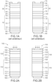
- the two subcells can be stacked on top of each other in a PIN/PIN pattern ( Figure 1A ) or PIN/PIN ( Figure 1B ).
- Lower electrodes 40 and upper electrodes 50 as well as electrical contacts 60, 70 complete the structure.
- Each sub-cell 10, 30 of the tandem structure comprises layers which allow the charges to be separated and selected according to their polarity.
- the recombination zone 20 between the two sub-cells is called a "recombination junction" because it allows the charges to recombine. Generally, it is formed by a transparent conductive oxide layer or a tunnel junction (two highly doped layers, one of type N and the other of type P). This recombination zone allows the series connection of the sub-cells and thus the addition of their voltages. It must cause the recombination of the electrons generated in the upper cell 30 and the holes generated in the lower cell 10 for a tandem of NIP structure ( Fig.1A ) and the reverse for a PIN structure ( Fig.1B ).
- tandem structures require many steps to be manufactured, which increases manufacturing costs and the number of layers and interfaces likely to reduce performance (by adding series resistance, contact resistances, unwanted recombinations, etc.).
- tandem NIP-type structure comprising a perovskite upper cell and a crystalline silicon and poly-Si based lower cell can operate by directly positioning the upper cell on the cell lower ( Shen et al. “In situ recombination junction between p-Si and TiO2 enables high-efficiency monolithic perovskite/Si tandem cells”, Science Advances, 2018; 4: eaau9711 ). More specifically, an N-type TiOz layer is deposited by ALD directly on the P-doped silicon of the lower cell. Then, a perovskite layer and a P-type PTAA layer are deposited. The operation of this structure is made possible by the low contact resistivity between the ALD TiOz layer and the P-doped silicon of the lower cell.
- tandem perovskite structure on silicon homojunction was fabricated by directly depositing the N-type SnOz layer of the upper perovskite cell onto the P-type layer of the lower cell ( Zheng et al. “Large area efficient interface layer free monolithic perovskite/homo-junction-silicon tandem solar cell with over 20% efficiency”, Energy Environ. Sci., 2018, 11, 2432-2443 ).
- An aim of the present invention is to provide a tandem perovskite structure on silicon heterojunction based on amorphous silicon and two-terminal crystalline silicon having good electrical properties and simpler and less expensive to manufacture.
- the present invention provides a 2-terminal tandem structure comprising the features of claim 1.
- the invention is fundamentally distinguished from the prior art by the use of a transparent conductive oxide (TCO) junction material which not only plays the role of recombination junction but also that of charge selection (N-type contact) for one of the cells in the tandem structure.
- TCO transparent conductive oxide
- N-type contact charge selection
- This simplified structure is simpler to manufacture compared to conventional tandem solar structures.
- the reduction in the number of steps in the manufacturing process leads to a reduction in manufacturing costs.
- the tandem structure is of the NIP type.
- the second cell is devoid of the N-type layer.
- the second cell is formed of the active layer in a perovskite material and the second layer of the P-type.
- the active layer in a perovskite material is then in direct contact with the TCO junction layer which thus plays the role of N-type layer for the NIP-type tandem structure.
- the (p)a-Si:H/TCO interface has good recombination properties and as the stacking of the lower cell is homogeneous, the deposition of the perovskite layer on the TCO is also homogeneous.
- the tandem structure is of the PIN type.
- the first cell is devoid of an N-type layer: the first cell is formed of the crystalline silicon substrate, covered on both sides by an intrinsic amorphous silicon layer, and the P-type layer (the P-type layer is the first layer of the stack starting from the rear face).
- the junction layer is in direct contact with the second intrinsic amorphous silicon layer.
- the upper perovskite cell here is a classical cell (i.e. the perovskite layer is deposited on the P-type layer). Such a cell is known and can be easily produced with classical methods.
- the junction layer has a thickness of 2 to 30 nm.
- the junction layer has a conductivity of greater than 10 S.cm -1 .
- the junction layer is made of ITO.
- the junction layer is made of AZO, ZnO, IWO, IZO, IZrO or SnO 2-x with x greater than 0 and strictly less than 2.
- the perovskite material has the formula Cs x FA 1-x Pb(I 1-y Br y ) 3 (with x ⁇ 0.20; 0 ⁇ y ⁇ 1).
- the tandem structure 100 may be a NIP type structure ( Figure 2A ) or PIN type ( Figure 2B ).
- the active layer 131 of the second cell 130 is directly in contact with the junction layer 120, so there is no layer interposed between the two.
- the second intrinsic amorphous silicon layer 114 of the first cell 110 is directly in contact with the junction layer 120; there is therefore no layer interposed between the two.
- the TCO junction layer 120 can have a thickness of 2 to 30 nm and preferably between 2 nm and 15 nm.
- the conductivity of the TCO junction layer 120 is, for example, greater than 10 S.cm -1 .
- the junction layer 120 may be indium tin oxide (ITO), zinc oxide (ZnO), aluminum-doped zinc oxide (AZO), indium tungsten oxide (IWO), indium zinc oxide (IZO), zirconium-doped indium oxide (IZrO) or tin dioxide (SnO 2-x with 0 ⁇ x ⁇ 2).
- the band gap of the 120 TCO junction layer ranges from 2.8 to 4 eV.
- the 120 ITO junction layer has a conduction band from -4.2 to -5.2 eV.
- the conduction band ranges from -4 to -5.2 eV.
- the junction layer 120 is made of ITO.
- the silicon substrate 12 of the lower cell can be polished or textured (for example, it can be a texturing in the form of 2 ⁇ m pyramids).
- the amorphous layers of the lower cell having a thickness of a few nanometers, they will take the form of the texturing of the substrate.
- the p/n doping rates of layers 111 and 115 are, for example, between 10 18 and 10 19 /cm 3 .
- the N-type layer 133 of the second perovskite cell is called the "electron transport layer” (or EIL for "Electron Injection Layer” or ETL for “Electron Transport Layer”).
- the N-type layer 133 is, for example, a metal oxide such as zinc oxide (ZnO), aluminum-doped zinc oxide also called AZO (ZnO:Al), titanium oxide (TiO 2 ) or tin oxide (SnO 2 ). It can also be a stack of [6,6]-phenyl-C 61 -methyl butanoate and SnOz (PCBM/SnO 2 ) or [6,6]-phenyl-C 61 -methyl butanoate and bathocuproine (PCBM/BCP).
- ZnO zinc oxide
- AZO ZnO:Al
- TiO 2 titanium oxide
- SnO 2 tin oxide
- PCBM/SnO 2 tin oxide
- the perovskite material of the active layer 131 of the second solar cell 130 has the general formula ABX 3 with A representing one or more monovalent organic cations, such as an ammonium, such as methylammonium or formamidinium, or a monovalent metal cation, such as cesium or rubidium; B representing a divalent metal cation such as Pb, Sn, Ag or one of their mixtures; and X representing one or more halide anions.
- A representing one or more monovalent organic cations, such as an ammonium, such as methylammonium or formamidinium, or a monovalent metal cation, such as cesium or rubidium
- B representing a divalent metal cation such as Pb, Sn, Ag or one of their mixtures
- X representing one or more halide anions.
- the perovskite material may have the particular formula H 2 NCHNH 2 PbX 3 or CH 3 NH 3 PbX 3 with X a halogen. It may be, for example, methylammonium lead iodide CH 3 NH 3 PbI 3 .
- the perovskite material has the formula Cs x FA 1-x Pb(I 1-y Br y ) 3 .
- the P-type layer 132 of the second cell 130 is also called the “hole transport layer” (or HTL for “Hole Transport Layer”).
- the P-type layer 132 is, for example, an organic compound such as Poly(3,4-ethylenedioxythiophene) Polystyrene sulfonate (PEDOT:PSS), [poly(bis 4-phenyl ⁇ 2,4,6-trimethylphenyl ⁇ amine)] (PTAA), [Poly( N,N' -bis(4-butylphenyl)- N,N' -bis(phenyl)-benzidine] (Poly-TPD), 2,2',7,7'-Tetrakis[N,N-di(4-methoxyphenyl)amino]-9,9'-spirobifluorene (spiro-OMeTAD), N4,N4'-bis(4-(6-((3-ethyloxetan-3-yl)methoxy)hexyl)phenyl)-N4,N4'-diphenyl-[1,1'-biphenyl]-4,4'-diamine (OT
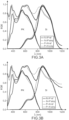
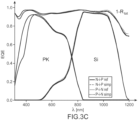
- Optical simulations of different structures were performed using CROWM software, taking into account the optical indices of the layers, their thickness and the surface state (totally flat, textured). These simulations are performed between 310 and 1200 nm with the AM1.5 solar spectrum. The optical indices were extracted by ellipsometry from the experimental layers.
- Table 1 lists the thicknesses (nm) of the simulated layers for NIP-type architectures.
- NIP reference structure Simplified NIP structure
- ITO front face 180 180 PTAA 30 30
- ITO junction layer 12
- 12 a-Si:H(p) 19 19 a-Si:H (i) 5 5 c-Yes 280000 280000 a-Si:H (i) 5 5 a-Si:H (n) 8 8 ITO back side 70 70 Ag 200 200
- Table 2 lists the thicknesses (nm) of the simulated layers for PIN-type architectures.
- PIN reference structure Simplified PIN structure ITO front face 180 180 SnO 2 30 30 Perovskite active layer 250 and 415 250 and 415 PTAA 30 30 Rec. ITO junction layer. 12 12 a-Si:H (n) 8 - a-Si:H (i) 5 5 c-Yes 280000 280000 a-Si:H (i) 5 5 a-Si:H(p) 19 19 ITO back side 70 70 Ag 200 200
- the perovskite used in the simulations is of type Cs x FA 1-x Pb(I 1-y Br y ) 3 (with x ⁇ 0.20; 0 ⁇ y ⁇ 1), two different thicknesses were used to obtain less current gap between the two sub-cells when the surface state is modified.
- results presented correspond to tandem structures whose active layer of the upper cell is a perovskite material 250 nm thick when the front face is polished and 415 nm thick when it is textured.
Landscapes
- Chemical & Material Sciences (AREA)
- Inorganic Chemistry (AREA)
- Physics & Mathematics (AREA)
- Electromagnetism (AREA)
- Photovoltaic Devices (AREA)
Claims (7)
- Photovoltaik-Tandemstruktur (100) mit 2-Terminals vom Typ PIN, von der Rückseite zur Vorderseite umfassend:- eine erste Siliziumsolarzelle (110) mit Heteroübergang, eine erste Schicht vom Typ P (115) aus dotiertem amorphem Silizium umfassend und ein dotiertes kristallines Siliziumsubstrat (112) vom Typ N, das zwischen einer ersten intrinsischen amorphen Siliziumschicht (113) und einer zweiten intrinsischen amorphen Siliziumschicht (114) angeordnet ist,- eine Verbindungsschicht (120),- eine zweite Solarzelle (130) vom Typ Perowskit, eine zweite Schicht vom Typ P (132), eine aktive Schicht (131) aus einem Perowskit-Material und eine Schicht vom Typ N (133) umfassend,dadurch gekennzeichnet, dass die Verbindungsschicht (120) aus transparentem leitfähigem Oxid (TCO) besteht,und dass die Verbindungsschicht (120) mit der zweiten intrinsischen amorphen Siliziumschicht (114) der ersten Solarzelle (110) und mit der zweiten Schicht vom Typ P (132) der zweiten Solarzelle (130) in Kontakt steht,wobei die Verbindungsschicht (120) als Schicht vom Typ N in der ersten Solarzelle (110) fungiert.
- Tandemstruktur (100) nach Anspruch 1, dadurch gekennzeichnet, dass die Verbindungsschicht (120) aus ITO besteht.
- Tandemstruktur (100) nach Anspruch 1, dadurch gekennzeichnet, dass die Verbindungsschicht (120) aus AZO, ZnO, IWO, IZO, IZrO oder SnO2-x mit x größer als 0 und streng kleiner als 2 besteht.
- Tandemstruktur (100) nach einem der vorhergehenden Ansprüche, dadurch gekennzeichnet, dass die Verbindungsschicht (120) eine Dicke von 2 bis 30 nm aufweist, und vorzugsweise zwischen 2 nm und 15 nm.
- Tandemstruktur (100) nach einem der vorhergehenden Ansprüche, dadurch gekennzeichnet, dass die Verbindungsschicht (120) eine Leitfähigkeit aufweist, die höher als 10 S.cm-1 ist.
- Tandemstruktur (100) nach einem der vorhergehenden Ansprüche, dadurch gekennzeichnet, dass die Tandemstruktur (100) von der Rückseite zur Vorderseite umfasst:- die erste Siliziumsolarzelle (110) mit Heteroübergang auf Basis von amorphem Silizium und kristallinem Silizium, von der Rückseite zur Vorderseite umfassend: die erste Schicht vom Typ P aus dotiertem amorphem Silizium (115), die erste intrinsische amorphe Siliziumschicht (113), das N-dotierte kristalline Siliziumsubstrat (112) und die zweite intrinsische amorphe Siliziumschicht (114),- die Verbindungsschicht (120) aus TCO vom Typ N,- die zweite Solarzelle (130) vom Typ Perowskit, vom Verbindungsmaterial zur Vorderseite umfassend: eine Schicht vom Typ P (132) aus PTAA oder TFB, die aktive Schicht (131) aus Perowskit-Material und eine Schicht vom Typ N (133), die aus SnOz gebildet ist oder aus einer Doppelschicht PCBM/SnOz.
- Tandemstruktur (100) nach einem der vorhergehenden Ansprüche, dadurch gekennzeichnet, dass das Perowskit-Material die Formel CsxFA1-xPb(I1-yBry)3 hat, (mit x < 0,20; 0 < y < 1).
Applications Claiming Priority (2)
| Application Number | Priority Date | Filing Date | Title |
|---|---|---|---|
| FR2013592A FR3118298B1 (fr) | 2020-12-18 | 2020-12-18 | Structure simplifiee de cellules solaires tandem a deux terminaux ayant un materiau de jonction en oxyde transparent conducteur |
| PCT/FR2021/052295 WO2022129757A1 (fr) | 2020-12-18 | 2021-12-13 | Structure simplifiee de cellules solaires tandem a deux terminaux ayant un materiau de jonction en oxyde transparent conducteur |
Publications (2)
| Publication Number | Publication Date |
|---|---|
| EP4264677A1 EP4264677A1 (de) | 2023-10-25 |
| EP4264677B1 true EP4264677B1 (de) | 2024-11-06 |
Family
ID=74554117
Family Applications (1)
| Application Number | Title | Priority Date | Filing Date |
|---|---|---|---|
| EP21848274.3A Active EP4264677B1 (de) | 2020-12-18 | 2021-12-13 | Vereinfachte struktur von doppelpol-tandemsolarzellen mit transparentem leitfähigem oxidverbindungsmaterial |
Country Status (8)
| Country | Link |
|---|---|
| US (1) | US12274110B2 (de) |
| EP (1) | EP4264677B1 (de) |
| CN (1) | CN117280479A (de) |
| AU (1) | AU2021402160A1 (de) |
| CA (1) | CA3202274A1 (de) |
| ES (1) | ES3011483T3 (de) |
| FR (1) | FR3118298B1 (de) |
| WO (1) | WO2022129757A1 (de) |
Family Cites Families (8)
| Publication number | Priority date | Publication date | Assignee | Title |
|---|---|---|---|---|
| TR201904847T4 (tr) * | 2015-06-12 | 2019-05-21 | Oxford Photovoltaics Ltd | Fotovoltai̇k ci̇haz |
| ES2977146T3 (es) * | 2015-06-12 | 2024-08-19 | Oxford Photovoltaics Ltd | Dispositivo fotovoltaico multiunión |
| GB201510351D0 (en) * | 2015-06-12 | 2015-07-29 | Oxford Photovoltaics Ltd | Method of depositioning a perovskite material |
| US20200313093A1 (en) * | 2016-05-20 | 2020-10-01 | Brown University | Method for Manufacturing Perovskite Solar Cells and Multijunction Photovoltaics |
| US11296244B2 (en) * | 2016-09-20 | 2022-04-05 | The Board Of Trustees Of The Leland Stanford Junior University | Solar cell comprising a metal-oxide buffer layer and method of fabrication |
| CN107369767A (zh) * | 2017-07-20 | 2017-11-21 | 南开大学 | 一种钙钛矿/硅异质结两端叠层太阳电池 |
| CN209016100U (zh) * | 2018-10-19 | 2019-06-21 | 君泰创新(北京)科技有限公司 | 一种钙钛矿/硅基异质结叠层太阳能电池 |
| CN111554764A (zh) * | 2020-04-01 | 2020-08-18 | 南开大学 | 一种高效稳定的钙钛矿/硅两端叠层太阳电池 |
-
2020
- 2020-12-18 FR FR2013592A patent/FR3118298B1/fr active Active
-
2021
- 2021-12-13 AU AU2021402160A patent/AU2021402160A1/en not_active Abandoned
- 2021-12-13 US US18/257,812 patent/US12274110B2/en active Active
- 2021-12-13 ES ES21848274T patent/ES3011483T3/es active Active
- 2021-12-13 CN CN202180092913.9A patent/CN117280479A/zh active Pending
- 2021-12-13 EP EP21848274.3A patent/EP4264677B1/de active Active
- 2021-12-13 CA CA3202274A patent/CA3202274A1/fr active Pending
- 2021-12-13 WO PCT/FR2021/052295 patent/WO2022129757A1/fr not_active Ceased
Also Published As
| Publication number | Publication date |
|---|---|
| EP4264677A1 (de) | 2023-10-25 |
| US12274110B2 (en) | 2025-04-08 |
| FR3118298A1 (fr) | 2022-06-24 |
| US20240107785A1 (en) | 2024-03-28 |
| AU2021402160A1 (en) | 2023-07-13 |
| CN117280479A (zh) | 2023-12-22 |
| CA3202274A1 (fr) | 2022-06-23 |
| ES3011483T3 (en) | 2025-04-07 |
| WO2022129757A1 (fr) | 2022-06-23 |
| AU2021402160A9 (en) | 2024-09-26 |
| FR3118298B1 (fr) | 2023-06-23 |
Similar Documents
| Publication | Publication Date | Title |
|---|---|---|
| CN108292688B (zh) | 含氧化物纳米颗粒缓冲层的太阳能电池和制造方法 | |
| CN1774823B (zh) | 带有有机层的光活性组件 | |
| JP4966653B2 (ja) | 共有する有機電極を備えたタンデム型光起電力電池及びその製造方法 | |
| US20200295209A1 (en) | Integration of bypass diodes within thin film photovoltaic module interconnects | |
| CN1806349B (zh) | 包括具有非对称传导特性的中间层的有机太阳能电池 | |
| US9768329B1 (en) | Multi-junction optoelectronic device | |
| CN114023889A (zh) | 钙钛矿太阳能电池组及其制备方法、光伏组件 | |
| EP3555921B1 (de) | Tandem-fotovoltaikzelle mit einer subzelle auf basis von perowskit und einer subzelle auf basis von silizium | |
| US11271128B2 (en) | Multi-junction optoelectronic device | |
| EP4264678A1 (de) | Vereinfachte tandemstruktur für solarzellen mit zwei anschlüssen | |
| JP7662130B2 (ja) | 金属酸窒化物層を有する多接合型光起電デバイス | |
| EP4264677B1 (de) | Vereinfachte struktur von doppelpol-tandemsolarzellen mit transparentem leitfähigem oxidverbindungsmaterial | |
| JP2006066707A (ja) | 光電変換装置 | |
| US20250185451A1 (en) | Tandem cell and photovoltaic module | |
| US20250037943A1 (en) | Integrated Bypass Diode Schemes for Solar Modules | |
| EP3979337A1 (de) | Verfahren zur charakterisierung einer solarzelle unter ähnlichen bedingungen wie bei einer solarvorrichtung mit tandem-architektur |
Legal Events
| Date | Code | Title | Description |
|---|---|---|---|
| STAA | Information on the status of an ep patent application or granted ep patent |
Free format text: STATUS: UNKNOWN |
|
| STAA | Information on the status of an ep patent application or granted ep patent |
Free format text: STATUS: THE INTERNATIONAL PUBLICATION HAS BEEN MADE |
|
| PUAI | Public reference made under article 153(3) epc to a published international application that has entered the european phase |
Free format text: ORIGINAL CODE: 0009012 |
|
| STAA | Information on the status of an ep patent application or granted ep patent |
Free format text: STATUS: REQUEST FOR EXAMINATION WAS MADE |
|
| 17P | Request for examination filed |
Effective date: 20230704 |
|
| AK | Designated contracting states |
Kind code of ref document: A1 Designated state(s): AL AT BE BG CH CY CZ DE DK EE ES FI FR GB GR HR HU IE IS IT LI LT LU LV MC MK MT NL NO PL PT RO RS SE SI SK SM TR |
|
| DAV | Request for validation of the european patent (deleted) | ||
| DAX | Request for extension of the european patent (deleted) | ||
| GRAP | Despatch of communication of intention to grant a patent |
Free format text: ORIGINAL CODE: EPIDOSNIGR1 |
|
| STAA | Information on the status of an ep patent application or granted ep patent |
Free format text: STATUS: GRANT OF PATENT IS INTENDED |
|
| RIC1 | Information provided on ipc code assigned before grant |
Ipc: H01L 31/0747 20120101ALI20240716BHEP Ipc: H01L 31/0725 20120101AFI20240716BHEP |
|
| INTG | Intention to grant announced |
Effective date: 20240730 |
|
| GRAS | Grant fee paid |
Free format text: ORIGINAL CODE: EPIDOSNIGR3 |
|
| GRAA | (expected) grant |
Free format text: ORIGINAL CODE: 0009210 |
|
| STAA | Information on the status of an ep patent application or granted ep patent |
Free format text: STATUS: THE PATENT HAS BEEN GRANTED |
|
| RAP3 | Party data changed (applicant data changed or rights of an application transferred) |
Owner name: 3SUN S.R.L. Owner name: COMMISSARIAT A L'ENERGIE ATOMIQUE ET AUX ENERGIESALTERNATIVES |
|
| AK | Designated contracting states |
Kind code of ref document: B1 Designated state(s): AL AT BE BG CH CY CZ DE DK EE ES FI FR GB GR HR HU IE IS IT LI LT LU LV MC MK MT NL NO PL PT RO RS SE SI SK SM TR |
|
| REG | Reference to a national code |
Ref country code: GB Ref legal event code: FG4D Free format text: NOT ENGLISH |
|
| REG | Reference to a national code |
Ref country code: CH Ref legal event code: EP |
|
| REG | Reference to a national code |
Ref country code: DE Ref legal event code: R079 Ref document number: 602021021611 Country of ref document: DE Free format text: PREVIOUS MAIN CLASS: H01L0031072500 Ipc: H10F0010161000 |
|
| REG | Reference to a national code |
Ref country code: DE Ref legal event code: R096 Ref document number: 602021021611 Country of ref document: DE |
|
| REG | Reference to a national code |
Ref country code: IE Ref legal event code: FG4D Free format text: LANGUAGE OF EP DOCUMENT: FRENCH |
|
| REG | Reference to a national code |
Ref country code: LT Ref legal event code: MG9D |
|
| REG | Reference to a national code |
Ref country code: NL Ref legal event code: MP Effective date: 20241106 |
|
| REG | Reference to a national code |
Ref country code: ES Ref legal event code: FG2A Ref document number: 3011483 Country of ref document: ES Kind code of ref document: T3 Effective date: 20250407 |
|
| PG25 | Lapsed in a contracting state [announced via postgrant information from national office to epo] |
Ref country code: IS Free format text: LAPSE BECAUSE OF FAILURE TO SUBMIT A TRANSLATION OF THE DESCRIPTION OR TO PAY THE FEE WITHIN THE PRESCRIBED TIME-LIMIT Effective date: 20250306 Ref country code: HR Free format text: LAPSE BECAUSE OF FAILURE TO SUBMIT A TRANSLATION OF THE DESCRIPTION OR TO PAY THE FEE WITHIN THE PRESCRIBED TIME-LIMIT Effective date: 20241106 Ref country code: PT Free format text: LAPSE BECAUSE OF FAILURE TO SUBMIT A TRANSLATION OF THE DESCRIPTION OR TO PAY THE FEE WITHIN THE PRESCRIBED TIME-LIMIT Effective date: 20250306 |
|
| PG25 | Lapsed in a contracting state [announced via postgrant information from national office to epo] |
Ref country code: FI Free format text: LAPSE BECAUSE OF FAILURE TO SUBMIT A TRANSLATION OF THE DESCRIPTION OR TO PAY THE FEE WITHIN THE PRESCRIBED TIME-LIMIT Effective date: 20241106 Ref country code: NL Free format text: LAPSE BECAUSE OF FAILURE TO SUBMIT A TRANSLATION OF THE DESCRIPTION OR TO PAY THE FEE WITHIN THE PRESCRIBED TIME-LIMIT Effective date: 20241106 |
|
| REG | Reference to a national code |
Ref country code: AT Ref legal event code: MK05 Ref document number: 1740391 Country of ref document: AT Kind code of ref document: T Effective date: 20241106 |
|
| PG25 | Lapsed in a contracting state [announced via postgrant information from national office to epo] |
Ref country code: BG Free format text: LAPSE BECAUSE OF FAILURE TO SUBMIT A TRANSLATION OF THE DESCRIPTION OR TO PAY THE FEE WITHIN THE PRESCRIBED TIME-LIMIT Effective date: 20241106 |
|
| PG25 | Lapsed in a contracting state [announced via postgrant information from national office to epo] |
Ref country code: NO Free format text: LAPSE BECAUSE OF FAILURE TO SUBMIT A TRANSLATION OF THE DESCRIPTION OR TO PAY THE FEE WITHIN THE PRESCRIBED TIME-LIMIT Effective date: 20250206 |
|
| PG25 | Lapsed in a contracting state [announced via postgrant information from national office to epo] |
Ref country code: LV Free format text: LAPSE BECAUSE OF FAILURE TO SUBMIT A TRANSLATION OF THE DESCRIPTION OR TO PAY THE FEE WITHIN THE PRESCRIBED TIME-LIMIT Effective date: 20241106 Ref country code: GR Free format text: LAPSE BECAUSE OF FAILURE TO SUBMIT A TRANSLATION OF THE DESCRIPTION OR TO PAY THE FEE WITHIN THE PRESCRIBED TIME-LIMIT Effective date: 20250207 Ref country code: AT Free format text: LAPSE BECAUSE OF FAILURE TO SUBMIT A TRANSLATION OF THE DESCRIPTION OR TO PAY THE FEE WITHIN THE PRESCRIBED TIME-LIMIT Effective date: 20241106 |
|
| PG25 | Lapsed in a contracting state [announced via postgrant information from national office to epo] |
Ref country code: PL Free format text: LAPSE BECAUSE OF FAILURE TO SUBMIT A TRANSLATION OF THE DESCRIPTION OR TO PAY THE FEE WITHIN THE PRESCRIBED TIME-LIMIT Effective date: 20241106 |
|
| PG25 | Lapsed in a contracting state [announced via postgrant information from national office to epo] |
Ref country code: IT Free format text: LAPSE BECAUSE OF NON-PAYMENT OF DUE FEES Effective date: 20241213 |
|
| PG25 | Lapsed in a contracting state [announced via postgrant information from national office to epo] |
Ref country code: RS Free format text: LAPSE BECAUSE OF FAILURE TO SUBMIT A TRANSLATION OF THE DESCRIPTION OR TO PAY THE FEE WITHIN THE PRESCRIBED TIME-LIMIT Effective date: 20250206 |
|
| PG25 | Lapsed in a contracting state [announced via postgrant information from national office to epo] |
Ref country code: SM Free format text: LAPSE BECAUSE OF FAILURE TO SUBMIT A TRANSLATION OF THE DESCRIPTION OR TO PAY THE FEE WITHIN THE PRESCRIBED TIME-LIMIT Effective date: 20241106 |
|
| PG25 | Lapsed in a contracting state [announced via postgrant information from national office to epo] |
Ref country code: DK Free format text: LAPSE BECAUSE OF FAILURE TO SUBMIT A TRANSLATION OF THE DESCRIPTION OR TO PAY THE FEE WITHIN THE PRESCRIBED TIME-LIMIT Effective date: 20241106 |
|
| PG25 | Lapsed in a contracting state [announced via postgrant information from national office to epo] |
Ref country code: EE Free format text: LAPSE BECAUSE OF FAILURE TO SUBMIT A TRANSLATION OF THE DESCRIPTION OR TO PAY THE FEE WITHIN THE PRESCRIBED TIME-LIMIT Effective date: 20241106 |
|
| PG25 | Lapsed in a contracting state [announced via postgrant information from national office to epo] |
Ref country code: RO Free format text: LAPSE BECAUSE OF FAILURE TO SUBMIT A TRANSLATION OF THE DESCRIPTION OR TO PAY THE FEE WITHIN THE PRESCRIBED TIME-LIMIT Effective date: 20241106 |
|
| PG25 | Lapsed in a contracting state [announced via postgrant information from national office to epo] |
Ref country code: SK Free format text: LAPSE BECAUSE OF FAILURE TO SUBMIT A TRANSLATION OF THE DESCRIPTION OR TO PAY THE FEE WITHIN THE PRESCRIBED TIME-LIMIT Effective date: 20241106 |
|
| PG25 | Lapsed in a contracting state [announced via postgrant information from national office to epo] |
Ref country code: CZ Free format text: LAPSE BECAUSE OF FAILURE TO SUBMIT A TRANSLATION OF THE DESCRIPTION OR TO PAY THE FEE WITHIN THE PRESCRIBED TIME-LIMIT Effective date: 20241106 |
|
| REG | Reference to a national code |
Ref country code: CH Ref legal event code: PL |
|
| REG | Reference to a national code |
Ref country code: DE Ref legal event code: R097 Ref document number: 602021021611 Country of ref document: DE |
|
| PG25 | Lapsed in a contracting state [announced via postgrant information from national office to epo] |
Ref country code: LU Free format text: LAPSE BECAUSE OF NON-PAYMENT OF DUE FEES Effective date: 20241213 |
|
| PG25 | Lapsed in a contracting state [announced via postgrant information from national office to epo] |
Ref country code: SE Free format text: LAPSE BECAUSE OF FAILURE TO SUBMIT A TRANSLATION OF THE DESCRIPTION OR TO PAY THE FEE WITHIN THE PRESCRIBED TIME-LIMIT Effective date: 20241106 |
|
| PLBE | No opposition filed within time limit |
Free format text: ORIGINAL CODE: 0009261 |
|
| STAA | Information on the status of an ep patent application or granted ep patent |
Free format text: STATUS: NO OPPOSITION FILED WITHIN TIME LIMIT |
|
| PG25 | Lapsed in a contracting state [announced via postgrant information from national office to epo] |
Ref country code: MC Free format text: LAPSE BECAUSE OF FAILURE TO SUBMIT A TRANSLATION OF THE DESCRIPTION OR TO PAY THE FEE WITHIN THE PRESCRIBED TIME-LIMIT Effective date: 20241106 |
|
| REG | Reference to a national code |
Ref country code: BE Ref legal event code: MM Effective date: 20241231 |
|
| 26N | No opposition filed |
Effective date: 20250807 |
|
| PG25 | Lapsed in a contracting state [announced via postgrant information from national office to epo] |
Ref country code: BE Free format text: LAPSE BECAUSE OF NON-PAYMENT OF DUE FEES Effective date: 20241231 |
|
| PG25 | Lapsed in a contracting state [announced via postgrant information from national office to epo] |
Ref country code: CH Free format text: LAPSE BECAUSE OF NON-PAYMENT OF DUE FEES Effective date: 20241231 |
|
| PG25 | Lapsed in a contracting state [announced via postgrant information from national office to epo] |
Ref country code: IE Free format text: LAPSE BECAUSE OF NON-PAYMENT OF DUE FEES Effective date: 20241213 |
|
| PG25 | Lapsed in a contracting state [announced via postgrant information from national office to epo] |
Ref country code: IT Free format text: LAPSE BECAUSE OF NON-PAYMENT OF DUE FEES Effective date: 20241213 |
|
| PGRI | Patent reinstated in contracting state [announced from national office to epo] |
Ref country code: IT Effective date: 20241231 |
|
| PGFP | Annual fee paid to national office [announced via postgrant information from national office to epo] |
Ref country code: FR Payment date: 20251223 Year of fee payment: 5 |
|
| PGFP | Annual fee paid to national office [announced via postgrant information from national office to epo] |
Ref country code: ES Payment date: 20260108 Year of fee payment: 5 |
|
| PGFP | Annual fee paid to national office [announced via postgrant information from national office to epo] |
Ref country code: DE Payment date: 20251229 Year of fee payment: 5 |
|
| PGFP | Annual fee paid to national office [announced via postgrant information from national office to epo] |
Ref country code: IT Payment date: 20251229 Year of fee payment: 5 |