EP4262091A1 - Calibration method for phase-locked loops and related circuit - Google Patents
Calibration method for phase-locked loops and related circuit Download PDFInfo
- Publication number
- EP4262091A1 EP4262091A1 EP23161535.2A EP23161535A EP4262091A1 EP 4262091 A1 EP4262091 A1 EP 4262091A1 EP 23161535 A EP23161535 A EP 23161535A EP 4262091 A1 EP4262091 A1 EP 4262091A1
- Authority
- EP
- European Patent Office
- Prior art keywords
- value
- halving
- read
- freq
- vco
- Prior art date
- Legal status (The legal status is an assumption and is not a legal conclusion. Google has not performed a legal analysis and makes no representation as to the accuracy of the status listed.)
- Granted
Links
Images



Classifications
-
- H—ELECTRICITY
- H03—ELECTRONIC CIRCUITRY
- H03L—AUTOMATIC CONTROL, STARTING, SYNCHRONISATION OR STABILISATION OF GENERATORS OF ELECTRONIC OSCILLATIONS OR PULSES
- H03L7/00—Automatic control of frequency or phase; Synchronisation
- H03L7/06—Automatic control of frequency or phase; Synchronisation using a reference signal applied to a frequency- or phase-locked loop
- H03L7/08—Details of the phase-locked loop
- H03L7/14—Details of the phase-locked loop for assuring constant frequency when supply or correction voltages fail
-
- H—ELECTRICITY
- H03—ELECTRONIC CIRCUITRY
- H03L—AUTOMATIC CONTROL, STARTING, SYNCHRONISATION OR STABILISATION OF GENERATORS OF ELECTRONIC OSCILLATIONS OR PULSES
- H03L7/00—Automatic control of frequency or phase; Synchronisation
- H03L7/06—Automatic control of frequency or phase; Synchronisation using a reference signal applied to a frequency- or phase-locked loop
- H03L7/08—Details of the phase-locked loop
- H03L7/099—Details of the phase-locked loop concerning mainly the controlled oscillator of the loop
- H03L7/0991—Details of the phase-locked loop concerning mainly the controlled oscillator of the loop the oscillator being a digital oscillator, e.g. composed of a fixed oscillator followed by a variable frequency divider
- H03L7/0992—Details of the phase-locked loop concerning mainly the controlled oscillator of the loop the oscillator being a digital oscillator, e.g. composed of a fixed oscillator followed by a variable frequency divider comprising a counter or a frequency divider
-
- H—ELECTRICITY
- H03—ELECTRONIC CIRCUITRY
- H03L—AUTOMATIC CONTROL, STARTING, SYNCHRONISATION OR STABILISATION OF GENERATORS OF ELECTRONIC OSCILLATIONS OR PULSES
- H03L7/00—Automatic control of frequency or phase; Synchronisation
- H03L7/06—Automatic control of frequency or phase; Synchronisation using a reference signal applied to a frequency- or phase-locked loop
- H03L7/08—Details of the phase-locked loop
- H03L7/085—Details of the phase-locked loop concerning mainly the frequency- or phase-detection arrangement including the filtering or amplification of its output signal
- H03L7/087—Details of the phase-locked loop concerning mainly the frequency- or phase-detection arrangement including the filtering or amplification of its output signal using at least two phase detectors or a frequency and phase detector in the loop
-
- H—ELECTRICITY
- H03—ELECTRONIC CIRCUITRY
- H03L—AUTOMATIC CONTROL, STARTING, SYNCHRONISATION OR STABILISATION OF GENERATORS OF ELECTRONIC OSCILLATIONS OR PULSES
- H03L7/00—Automatic control of frequency or phase; Synchronisation
- H03L7/06—Automatic control of frequency or phase; Synchronisation using a reference signal applied to a frequency- or phase-locked loop
- H03L7/08—Details of the phase-locked loop
- H03L7/085—Details of the phase-locked loop concerning mainly the frequency- or phase-detection arrangement including the filtering or amplification of its output signal
-
- H—ELECTRICITY
- H03—ELECTRONIC CIRCUITRY
- H03L—AUTOMATIC CONTROL, STARTING, SYNCHRONISATION OR STABILISATION OF GENERATORS OF ELECTRONIC OSCILLATIONS OR PULSES
- H03L7/00—Automatic control of frequency or phase; Synchronisation
- H03L7/06—Automatic control of frequency or phase; Synchronisation using a reference signal applied to a frequency- or phase-locked loop
- H03L7/08—Details of the phase-locked loop
- H03L7/099—Details of the phase-locked loop concerning mainly the controlled oscillator of the loop
-
- H—ELECTRICITY
- H03—ELECTRONIC CIRCUITRY
- H03L—AUTOMATIC CONTROL, STARTING, SYNCHRONISATION OR STABILISATION OF GENERATORS OF ELECTRONIC OSCILLATIONS OR PULSES
- H03L7/00—Automatic control of frequency or phase; Synchronisation
- H03L7/06—Automatic control of frequency or phase; Synchronisation using a reference signal applied to a frequency- or phase-locked loop
- H03L7/08—Details of the phase-locked loop
- H03L7/10—Details of the phase-locked loop for assuring initial synchronisation or for broadening the capture range
- H03L7/101—Details of the phase-locked loop for assuring initial synchronisation or for broadening the capture range using an additional control signal to the controlled loop oscillator derived from a signal generated in the loop
- H03L7/102—Details of the phase-locked loop for assuring initial synchronisation or for broadening the capture range using an additional control signal to the controlled loop oscillator derived from a signal generated in the loop the additional signal being directly applied to the controlled loop oscillator
- H03L7/103—Details of the phase-locked loop for assuring initial synchronisation or for broadening the capture range using an additional control signal to the controlled loop oscillator derived from a signal generated in the loop the additional signal being directly applied to the controlled loop oscillator the additional signal being a digital signal
-
- H—ELECTRICITY
- H03—ELECTRONIC CIRCUITRY
- H03L—AUTOMATIC CONTROL, STARTING, SYNCHRONISATION OR STABILISATION OF GENERATORS OF ELECTRONIC OSCILLATIONS OR PULSES
- H03L7/00—Automatic control of frequency or phase; Synchronisation
- H03L7/06—Automatic control of frequency or phase; Synchronisation using a reference signal applied to a frequency- or phase-locked loop
- H03L7/08—Details of the phase-locked loop
- H03L7/10—Details of the phase-locked loop for assuring initial synchronisation or for broadening the capture range
- H03L7/113—Details of the phase-locked loop for assuring initial synchronisation or for broadening the capture range using frequency discriminator
-
- H—ELECTRICITY
- H03—ELECTRONIC CIRCUITRY
- H03L—AUTOMATIC CONTROL, STARTING, SYNCHRONISATION OR STABILISATION OF GENERATORS OF ELECTRONIC OSCILLATIONS OR PULSES
- H03L2207/00—Indexing scheme relating to automatic control of frequency or phase and to synchronisation
- H03L2207/06—Phase locked loops with a controlled oscillator having at least two frequency control terminals
Definitions
- phase-locked loop or phase lock circuits, currently referred to with the acronym PLL.
- Phase-locked loop circuits have been used in a wide variety of possible applications, with renewed interest stimulated in recent times in areas such as automotive radar/digital radio, for advanced driver assistance system (ADAS) and infotainment applications, for instance.
- ADAS advanced driver assistance system
- infotainment applications for instance.
- a PLL circuit comprises a variable frequency oscillator (VCO) controlled by a detector that compares the phase of the VCO signal with the phase of the input signal and drives the oscillator to keep those phases in a matched (“locked") relationship.
- VCO variable frequency oscillator
- Low-noise performance of a PLL circuit involves a trade-off with the VCO (analog) tuning range.
- a capacitor bank controlled by digital switching bits can be used to compensate process variations in the synthesized operating frequency.
- a problem arising when finding a correct analog tuning range in high-frequency VCOs lies in that the digital capacitor(s) may give rise to non-monotonous characteristics. This phenomenon is related to parasitic connections that cannot be easily balanced for a resonator with many bits.
- Documents such as CN 101 951 259 A , US 8 872 556 B1 , and US 2009/115537 A1 are exemplary of background art in that area.
- An object of one or more embodiments is to contribute in adequately addressing the problem discussed in the foregoing.
- One or more embodiments relate to a corresponding circuit.
- Examples as discussed herein facilitate (automatically) finding an adequate VCO tuning range at PLL start-up also in the presence of a capacitor bank giving rise to a non-monotonous VCO characteristic.
- Examples as discussed herein provide a VCO calibration technique for PLL circuits wherein a finite state machine (FSM) uses a dichotomous procedure in searching a capacitance value that facilitates the VCO in setting an adequate (central) frequency for PLL calibration.
- FSM finite state machine
- An FSM-based calibration procedure facilitates VCO calibration and reaching PLL lock even in conditions of non-monotonicity of the VCO characteristic.
- Examples as discussed herein offer advantages such as recovery from non-monotonous VCO characteristic and countering undesired infinite bounce-among-steps operation, with error report.
- references to "an embodiment” or “one embodiment” in the framework of the present description is intended to indicate that a particular configuration, structure, or characteristic described in relation to the embodiment is comprised in at least one embodiment.
- phrases such as “in an embodiment”, “in one embodiment”, or the like, that may be present in various points of the present description do not necessarily refer exactly to one and the same embodiment.
- particular configurations, structures, or characteristics may be combined in any adequate way in one or more embodiments.
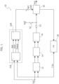
- FIG. 1 is a block diagram of a phase-locked loop (phase lock) circuit 10, currently referred to as PLL.
- reference 12 denotes a phase frequency detector (PFD) that receives an input signal at a certain frequency f ref and a (local) comparison signal at a frequency f div produced as discussed in the following.
- PFD phase frequency detector
- the output signal from the PFD 12 is applied to a charge pump (CP) 14 whose output is in turn applied to a (e.g., low-pass) loop filter (LF) 16 to control a voltage-controlled oscillator (VCO) 18.
- CP charge pump
- LF loop filter
- VCO voltage-controlled oscillator
- the VCO outputs an output signal at an oscillation frequency f out that is proportional to an input voltage applied thereto and "phase-locked" (hence the designation of the circuit) to the input signal f ref .
- the output signal from the VCO 18 is used to close the loop on the PFD 12 via a 1/N frequency divider 20 that produces the comparison signal at a frequency f div .
- Adequate locking of the PLL is facilitated by the VCO 18 being operated in an analog tuning range capable of synthesizing the frequency f out of interest.
- the VCO 18 can be "calibrated” by opening the loop at a switch S1 upstream of the VCO 18 that is coupled to a reference signal v ref via a second switch S2 (this is open, that is non-conductive, in normal operation).
- AFC automatic frequency control
- the AFC code is produced in an open-loop arrangement of a frequency detector 22A that receives the input signal f ref and the frequency-divided signal f div and controls a finite state machine (FSM) 22B via fast, slow, and freeze signals during the calibration procedure.
- FSM finite state machine
- the FSM 22B outputs an n-bit (e.g., a four-bit) AFC code b 0 , b 1 , b 2 , b 3 , ..., b n that is used to compensate process variations in the synthesized operating frequency of the VCO 18 via a capacitor bank controlled by digital switching bits based on the signals fast, slow, freeze.
- a capacitor/capacitance bank can be termed a "digital" one insofar as its values are determined based on a digital word (the AFC code, e.g., b 0 , b 1 , b 2
- a problem in finding an adequate analog tuning range lies that the "digital" capacitance used to calibrate the VCO 18 exhibits a non-monotonous characteristic. This is related to parasitic connections that cannot be easily balanced for a resonator with many bits.
- a capacitor bank (e.g., with capacitors suited to individually activated/deactivated) is associated to the VCO 18 controlled by digital switching bits such as, e.g., b 0 , b 1 , b 2 , b 3 .
- digital switching bits such as, e.g., b 0 , b 1 , b 2 , b 3 .
- Examples discussed herein thus address the problem of automatically finding an analog tuning range at circuit start-up also in the presence of case of a ("digital") capacitor bank providing non-monotonous VCO characteristics.
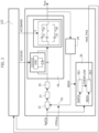
- Figure 2 is a block diagram of a PLL circuit configured to apply embodiments of the present description.
- a PLL circuit 10 as illustrated in Figure 2 thus comprises a phase frequency detector (PFD) 12, a charge pump (CP) 14, a low-pass filter (LPF) 16, a voltage-controlled oscillator (VCO) 18 and an integer/fractional/sigma-delta) N frequency divider 20 (e.g., a 1/192 frequency divider).
- PFD phase frequency detector
- CP charge pump
- LPF low-pass filter
- VCO voltage-controlled oscillator
- N frequency divider 20 e.g., a 1/192 frequency divider
- NDIV divided output frequency
- RefClk reference clock signal
- the counter 26 outputs a frequency read_freq towards a finite state machine (FSM) 122.
- the FSM 122 facilitates calibrating (automatically) the VCO 18 based on the frequency read by the counter 26 via control information (signals) for the VCO 18 designated VCOBAND (coarse calibration) and VCODAC (fine calibration). Calibration of the VCO 18 via the FSM 122 takes place in an open-loop operation, with a switch OL controlled by a signal CPStop from the FSM 122, switched "open", that is, made non-conductive (see also the switches S1 and S2 in Figure 1 ).
- the signals VCOBAND (coarse calibration) and VCODAC (fine calibration) facilitate selecting an adequate value for the "digital" capacitance (e.g., the AFC code comprised of the bit word b 0 , b 1 , b 2 , b 3 , ..., b n ) to achieve a desired frequency of operation of the VCO 18.
- the FSM 122 is also configured to report end of calibration, as well as error in case of calibration failure.
- Figure 3 is a flow chart exemplary of possible operation of a PLL circuit 10 as illustrated in Figure 2 , assuming, for the time being, a monotonous VCO characteristic.
- the procedure exemplified by the flow chart of Figure 3 starts with PLL enable (block 1000), opening the loop (block 1001 - see also the switches S1 and S2 in Figure 1 , not reproduced in Figure 2 for simplicity) and initializing the variables for the procedure (block 1002), with the frequency count started.
- a new maximum value (new_max) is set in block 1006 equal to the old one (old_max) with a new center value set to (old_max+old_min)/2 with a new minimum value (new_min) set to the old one (old_min).
- new_max is set in block 1008 to the old one (old_max) with a new center value set to (old_max+old_min)/2 with a new minimum value (new_min) set to the old center value (old_center)
- the coarse calibration procedure and the fine calibration may include interval re-assignment options that are mutually complementary (inverted).
- the FSM 122 can be configured to perform a dichotomous search as discussed previously based on five (5) states:
- a recovery feature can be envisaged if calibration fails, in order to avoid an infinite "bouncing" around a certain.
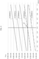
- Figure 5 shows an (exemplary) diagram of VCO frequency Fvco versus VCO tuning voltage Vtune for various VCO bands (e.g., VCOBAND 11, VCOBAND 12, VCOBAND 13, VCOBAND 14, VCOBAND 15) referring to a monotonous VCO characteristic.
- VCO bands e.g., VCOBAND 11, VCOBAND 12, VCOBAND 13, VCOBAND 14, VCOBAND 15
- a four-bit "digital" capacitor bank is of course merely exemplary: for instance, five bits and nine bits can be used for coarse tuning (VCOBAND) and fine tuning (VCODAC), respectively.
- Figure 7 is a diagram exemplary of a case of non-monotonicity of the VCO characteristic. Assuming that the capacitive value increases as VCOBAND increases, the trend may be non-linear: e.g., 11-14-13-12-15.
- the frequency counter 26 can include two (inner) counters 261 and 262.
- the former counter 261 is an N-bit counter that counts the reference signal RefClk over a count window.
- the latter counter 262 is a (N+1)-bit counter that counts the divide clock NDIV.
- the N-bit counter once at overflow, stops the (N+1)-bit counter 262 that can have a value higher or lower than 2 ⁇ N. A comparison will then be made (as discussed in the following) between such a value and 2 ⁇ N plus or minus a tolerance (+/- tol).
- Corresponding operation may be based on the procedure exemplified in Figures 8 , and 9A , 9B .
- Such a procedure can be regarded as an improvement suited to be applied to the procedure exemplified by blocks 1004 to 1012 (coarse calibration) and 1012 to 1021 (fine calibration) in the flow-chart of Figure 3 .
- the binary search procedure for a VCO calibration frequency starts with two preliminary steps represented by the blocks 3000a and 3000b.
- the step 3000b corresponds to an increase of i by one (i++).
- step 3000a the first value for store_read_freq[0] is set without making comparisons.
- step 3000b the value for store_read_freq[1] is set and the first comparison is made, and the procedure goes on with block 3000, where binary search halving is started where store_read_freq[i] is set equal to read_freq (as read from the counter 262 in the block 26) .
- the binary search halving index is increased by one (#i+1) at block 3002 and the procedure returns to block 3000.
- a check is made in a block 3003 comparing read_freq with f_des plus or minus a tolerance value tol.
- the binary search then proceeds back to block 3000 until the index i reaches the threshold value N.
- FIGs of Figures 9A and 9B show a (much) faster advance from VCOBAND (coarse) calibration to VCODAC (fine) calibration in the case of Figure 9A .
- the representation of Figure 10 further highlights that the PLL VCO calibration technique presented herein facilitates an FSM such as the FSM 122 in performing a dichotomous procedure in searching an adequate "digital" capacitance (e.g., an AFC code such as b 0 , b 1 , b 2 , b 3 ) to calibrate (tune) the VCO by setting a correct central frequency.
- an FSM such as the FSM 122 in performing a dichotomous procedure in searching an adequate "digital" capacitance (e.g., an AFC code such as b 0 , b 1 , b 2 , b 3 ) to calibrate (tune) the VCO by setting a correct central frequency.
- an adequate "digital" capacitance e.g., an AFC code such as b 0 , b 1 , b 2 , b 3
- the FSM 122 operates in open-loop condition, with a constant Vtune voltage (e.g., 0.5V), with the capability of facilitating PLL lock-in even in conditions of non-monotonicity of the VCO characteristic.
- Vtune voltage e.g. 0.5V
- Figure 10 refers, purely by way of example, to a dichotomous procedure starting with 32 (thirty-two, namely 2 5 ) "candidate" frequencies between a minimum (lower bound) frequency min (labelled 0) and a maximum (upper bound) frequency max (labelled 31) .
Landscapes
- Stabilization Of Oscillater, Synchronisation, Frequency Synthesizers (AREA)
Abstract
Description
- The description relates to phase-locked loop (or phase lock) circuits, currently referred to with the acronym PLL.
- Phase-locked loop circuits have been used in a wide variety of possible applications, with renewed interest stimulated in recent times in areas such as automotive radar/digital radio, for advanced driver assistance system (ADAS) and infotainment applications, for instance.
- In its simplest form, a PLL circuit comprises a variable frequency oscillator (VCO) controlled by a detector that compares the phase of the VCO signal with the phase of the input signal and drives the oscillator to keep those phases in a matched ("locked") relationship.
- Low-noise performance of a PLL circuit involves a trade-off with the VCO (analog) tuning range.
- A capacitor bank controlled by digital switching bits can be used to compensate process variations in the synthesized operating frequency.
- A problem arising when finding a correct analog tuning range in high-frequency VCOs lies in that the digital capacitor(s) may give rise to non-monotonous characteristics. This phenomenon is related to parasitic connections that cannot be easily balanced for a resonator with many bits.
- Documents such as
CN 101 951 259 A ,US 8 872 556 B1 , andUS 2009/115537 A1 are exemplary of background art in that area. - An object of one or more embodiments is to contribute in adequately addressing the problem discussed in the foregoing.
- According to examples described herein, such an object is achieved via a method having the features set forth in the claims that follow.
- One or more embodiments relate to a corresponding circuit.
- The claims are an integral part of the technical teaching provided herein in respect of the embodiments.
- Examples as discussed herein facilitate (automatically) finding an adequate VCO tuning range at PLL start-up also in the presence of a capacitor bank giving rise to a non-monotonous VCO characteristic.
- Examples as discussed herein provide a VCO calibration technique for PLL circuits wherein a finite state machine (FSM) uses a dichotomous procedure in searching a capacitance value that facilitates the VCO in setting an adequate (central) frequency for PLL calibration.
- In examples as discussed herein, such a finite state machine may operate in open-loop conditions, with a constant tuning voltage (e.g., Vtune = 0.5V).
- An FSM-based calibration procedure according to examples discussed herein facilitates VCO calibration and reaching PLL lock even in conditions of non-monotonicity of the VCO characteristic.
- Examples as discussed herein offer advantages such as recovery from non-monotonous VCO characteristic and countering undesired infinite bounce-among-steps operation, with error report.
- One or more embodiments will now be described, by way of example only, with reference to the annexed figures, wherein:
-
Figure 1 is a block diagram of a conventional PLL circuit, -
Figure 2 is a block diagram of a PLL circuit configured to apply embodiments of the present description, -
Figure 3 is a flow chart exemplary of a coarse-fine PLL calibration procedure, -
Figure 4 is a further flow chart exemplary of possible details of embodiments of the present description, -
Figures 5 ,6 , and7 are diagram exemplary of operation of embodiments of the present description withFigure 6 being an enlarged view of the portion ofFigure 5 indicated by arrow VI, -
Figure 8 is a further flow chart exemplary of possible details of embodiments of the present description, -
Figures 9A and9B are diagrams exemplary of operation of embodiments of the present description, and -
Figure 10 summarizes a possible practical implementation of embodiments of the present description. - Corresponding numerals and symbols in the different figures generally refer to corresponding parts unless otherwise indicated.
- The figures are drawn to clearly illustrate the relevant aspects of the embodiments and are not necessarily drawn to scale.
- The edges of features drawn in the figures do not necessarily indicate the termination of the extent of the feature.
- In the ensuing description, various specific details are illustrated in order to provide an in-depth understanding of various examples of embodiments according to the description. The embodiments may be obtained without one or more of the specific details, or with other methods, components, materials, etc. In other cases, known structures, materials, or operations are not illustrated or described in detail so that various aspects of the embodiments will not be obscured.
- Reference to "an embodiment" or "one embodiment" in the framework of the present description is intended to indicate that a particular configuration, structure, or characteristic described in relation to the embodiment is comprised in at least one embodiment. Hence, phrases such as "in an embodiment", "in one embodiment", or the like, that may be present in various points of the present description do not necessarily refer exactly to one and the same embodiment. Furthermore, particular configurations, structures, or characteristics may be combined in any adequate way in one or more embodiments.
- The headings/references used herein are provided merely for convenience and hence do not define the extent of protection or the scope of the embodiments.
-
Figure 1 is a block diagram of a phase-locked loop (phase lock)circuit 10, currently referred to as PLL. - In
Figure 1 ,reference 12 denotes a phase frequency detector (PFD) that receives an input signal at a certain frequency fref and a (local) comparison signal at a frequency fdiv produced as discussed in the following. - The output signal from the
PFD 12 is applied to a charge pump (CP) 14 whose output is in turn applied to a (e.g., low-pass) loop filter (LF) 16 to control a voltage-controlled oscillator (VCO) 18. - The VCO outputs an output signal at an oscillation frequency fout that is proportional to an input voltage applied thereto and "phase-locked" (hence the designation of the circuit) to the input signal fref.
- The output signal from the
VCO 18 is used to close the loop on thePFD 12 via a 1/N frequency divider 20 that produces the comparison signal at a frequency fdiv. - Adequate locking of the PLL is facilitated by the
VCO 18 being operated in an analog tuning range capable of synthesizing the frequency fout of interest. - To that effect, the
VCO 18 can be "calibrated" by opening the loop at a switch S1 upstream of theVCO 18 that is coupled to a reference signal vref via a second switch S2 (this is open, that is non-conductive, in normal operation). - Under these conditions, a n-bit (e.g., n = 4) automatic frequency control (AFC) code is applied to the
VCO 18. As illustrated inFigure 1 , the AFC code is produced in an open-loop arrangement of afrequency detector 22A that receives the input signal fref and the frequency-divided signal fdiv and controls a finite state machine (FSM) 22B via fast, slow, and freeze signals during the calibration procedure. - As illustrated in
Figure 1 theFSM 22B outputs an n-bit (e.g., a four-bit) AFC code b0, b1, b2, b3, ..., bn that is used to compensate process variations in the synthesized operating frequency of theVCO 18 via a capacitor bank controlled by digital switching bits based on the signals fast, slow, freeze. Such a capacitor/capacitance bank can be termed a "digital" one insofar as its values are determined based on a digital word (the AFC code, e.g., b0, b1, b2 - Architecture and operation of a PLL circuit as discussed so far are conventional in the art, which makes it unnecessary to provide a more detailed description herein.
- Architecture and operation of a PLL circuit as discussed herein are otherwise exemplary of a wide variety of PLL architectures where the same issues discussed in the following may arise.
- As a consequence, the examples presented herein shall not be construed, even indirectly, as limited to the exemplary architecture of a
PLL circuit 10 as discussed herein. - Whatever the specific implementation, a problem (encountered primarily with high-frequency VCOs) in finding an adequate analog tuning range lies that the "digital" capacitance used to calibrate the
VCO 18 exhibits a non-monotonous characteristic. This is related to parasitic connections that cannot be easily balanced for a resonator with many bits. - To summarize:
- adequate locking of a PLL circuit is facilitated by the VCO therein being in an analog tuning range capable of synthesizing the frequency of interest;
- PLL performance (primarily low-noise performance) involves a trade-off with the VCO analog tuning range: circuits with a narrow analog tuning range exhibit better phase noise performance;
- in order to compensate process variation in the synthesized operating frequency, a capacitor bank (e.g., with capacitors suited to individually activated/deactivated) is associated to the
VCO 18 controlled by digital switching bits such as, e.g., b0, b1, b2, b3. For instance (these quantitative figures are merely exemplary) an analog VCO tuning range TR = 150MHz facilitates achieving a total tuning range TR = 1.5GHz (including switching capacitors); and
a problem likely to arise in finding a correct analog tuning range lies in that such a digital capacitance provides non-monotonous characteristics, due to parasitic connections that cannot be easily balanced for a resonator with many bits. - Examples discussed herein thus address the problem of automatically finding an analog tuning range at circuit start-up also in the presence of case of a ("digital") capacitor bank providing non-monotonous VCO characteristics.
-
Figure 2 is a block diagram of a PLL circuit configured to apply embodiments of the present description. - Unless otherwise indicated, corresponding numerals and symbols in the figures generally refer to corresponding parts: a detailed description will not be repeated for each figure for brevity, being otherwise understood that certain parts or elements being indicated with a same reference in plural figures does not imply that these parts or elements shall be implemented in the same manner.
- A
PLL circuit 10 as illustrated inFigure 2 thus comprises a phase frequency detector (PFD) 12, a charge pump (CP) 14, a low-pass filter (LPF) 16, a voltage-controlled oscillator (VCO) 18 and an integer/fractional/sigma-delta) N frequency divider 20 (e.g., a 1/192 frequency divider). -
Reference 26 denotes is a counter that "counts" the divided output frequency NDIV (e.g., 50MHz = 9.6GHz/192) from thedivider 20 and also receives the reference clock signal RefClk that is applied to thePFD 12. - The
counter 26 outputs a frequency read_freq towards a finite state machine (FSM) 122. TheFSM 122 facilitates calibrating (automatically) theVCO 18 based on the frequency read by thecounter 26 via control information (signals) for theVCO 18 designated VCOBAND (coarse calibration) and VCODAC (fine calibration). Calibration of theVCO 18 via theFSM 122 takes place in an open-loop operation, with a switch OL controlled by a signal CPStop from theFSM 122, switched "open", that is, made non-conductive (see also the switches S1 and S2 inFigure 1 ). - The signals VCOBAND (coarse calibration) and VCODAC (fine calibration) facilitate selecting an adequate value for the "digital" capacitance (e.g., the AFC code comprised of the bit word b0, b1, b2, b3, ..., bn) to achieve a desired frequency of operation of the
VCO 18. - As discussed in the following, the
FSM 122 is also configured to report end of calibration, as well as error in case of calibration failure. -
Figure 3 is a flow chart exemplary of possible operation of aPLL circuit 10 as illustrated inFigure 2 , assuming, for the time being, a monotonous VCO characteristic. - The meaning of the blocks in the flow chart of
Figure 3 - where, in the blocks involving a check, YES denotes a positive outcome and NO denotes a negative outcome - is reproduced in the following list; further explanations on the steps represented by the blocks are given in the description following the list. - Block 1000: enable PLL/FSM
- Block 1001: initialize
- Block 1002: variable initialization - start count in
counter 26 - Block 1003: FRQCNTOVF = 1; frequency count overflow
- Block 1004: CAL_VCOBAND; calibrate VCO band
- Block 1005: read_freq > f_des + tol; frequency read higher than desired plus tolerance
- Block 1006: max_BAND = centr_BAND; min_BAND = min_BAND
- Block 1007: read_freq < f_des - tol; frequency read lower than desired minus tolerance
- Block 1008: max_BAND = max_BAND; min_BAND = centr_BAND
- Block 1009: idle; from the output of either of
blocks block 1007, OR from the output of either ofblocks block 1021. - Block 1010: centr = (max + min)/2 (for coarse calibration) OR centr _DAC = (max_DAC + min_DAC)/2 (for fine calibration); restart count
- Block 1011: FRQCNTOVF = 1; frequency count overflow
- Block 1012: end of VCOBAND (coarse) calibration
- Block 1013: VCOBAND = centr_BAND
- Block 1014: end Of VCODAC (fine) calibration
- Block 1015: VCODAC = centr_DAC
- Block 1016: EO_CAL
- Block 1017: CAL_VCODAC
- Block 1018: read_freq < f_des - tol; frequency read lower than desired minus tolerance
- Block 1019: max_DAC = centr_DAC; min_DAC = min_DAC
- Block 1020: read_freq > f_des + tol; frequency read higher than desired plus tolerance
- Block 1021: max_DAC = max_DAC; min_DAC = centr_DAC
- As noted, from the output of either of
blocks block 1020, the procedure evolves towards the idle state ofblock 1009. - To summarize, the procedure exemplified by the flow chart of
Figure 3 starts with PLL enable (block 1000), opening the loop (block 1001 - see also the switches S1 and S2 inFigure 1 , not reproduced inFigure 2 for simplicity) and initializing the variables for the procedure (block 1002), with the frequency count started. - At the end of the count (outcome YES of block 1003), in
blocks - At this point, new extremes and a new center are set in
blocks - If read_freq is higher than f_des_cycle + tol (positive outcome YES of block 1005) a new maximum value (new_max) is set in
block 1006 equal to the old one (old_max) with a new center value set to (old_max+old_min)/2 with a new minimum value (new_min) set to the old one (old_min). - If read_freq is lower than f_des_cycle - tol (positive outcome Y of block 1007) new_max is set in
block 1008 to the old one (old_max) with a new center value set to (old_max+old_min)/2 with a new minimum value (new_min) set to the old center value (old_center) - If read_freq is included in the range [f_des_cycle - tol; f_des_cycle + tol], in response to negative outcomes from both
blocks - This point marks the end of a VCOBAND search (coarse calibration, e.g., tol = 6), and the
FSM 122 starts a VCODAC search (fine calibration) followingsteps 1011 to 1021 similar to thesteps 1003 to 1008 discussed above, but using a lower tolerance value (e.g., tol= +/-1). - It is otherwise noted, the coarse calibration procedure and the fine calibration may include interval re-assignment options that are mutually complementary (inverted).
- The
FSM 122 can be configured to perform a dichotomous search as discussed previously based on five (5) states: - an INIT state, for initialization and first count;
- an IDLE state, for halving and for counts;
- a CAL_VCOBAND state, for read frequency comparison and re-assignment of range extremes for VCOBAND (coarse) calibration;
- a CAL_VCODAC state, for frequency reading comparison and re-assignment of range extremes for VCODAC (fine) calibration; and
- an EO_CAL state, for calibration end.
- A recovery feature can be envisaged if calibration fails, in order to avoid an infinite "bouncing" around a certain.
- For instance:
- for VCOBAND (coarse) calibration one can select a 5-bit vector for VCOBAND, with a maximum of 5 internal steps foreseen for calibration (plus 2 of tolerance).
- for VCODAC (fine) calibration one can select a 9-bit vector for VCODAC with a maximum of 9 internal steps foreseen for calibration (plus 2 of tolerance)
- Consequently, a maximum of, e.g., M=7 steps for VCOBAND calibration and of, e.g., M=11 steps for VCODAC calibration can be selected. When the number of steps reaches the relative threshold, an error signal report the failure.
- This mode of operation can be implemented in the
FSM 122 as exemplified in the flow-chart ofFigure 4 , where theblocks 2000 to 2004 have the following meaning: - block 2000 - binary search halving started with
step # 1; - block 2001 - step count increased
- block 2002 - current step count compared with threshold M (e.g., M=7 for VCOBAND and, e.g., M=11 for VCODAC), if threshold not reached yet (NO), back to
block 2000 - block 2003 - in response to threshold M reached (YES in block 2002) calibration error message issued.
- By way of further explanation,
Figure 5 shows an (exemplary) diagram of VCO frequency Fvco versus VCO tuning voltage Vtune for various VCO bands (e.g.,VCOBAND 11,VCOBAND 12,VCOBAND 13,VCOBAND 14, VCOBAND 15) referring to a monotonous VCO characteristic. - This representation assumes that, at the end of open-loop calibration, the
FSM 122 has set, e.g., VCOBAND = 14, VCODAC = 255 with Vtune = 0.5V (these values are, of course, merely exemplary). -
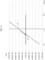
Figure 6 is an enlarged view of the portion ofFigure 6 indicated by arrow VII, showing that, when theFSM 122 closes the loop (switch OL closed, that is, made conductive again) a point A in the last step in open-loop calibration (block 1016 inFigure 2 corresponds to Vtune = 0.5V and Fvco = 9.604 GHz in fact "moves" to a point B corresponding to Vtune = 0.468V and Fvco = 9.6 GHz. - It is again recalled that a four-bit "digital" capacitor bank based on bits b0, b1, b2, and b3 (makes it possible to produce 24 = 16 (sixteen) VCO bands. Referring to a four-bit "digital" capacitor bank is of course merely exemplary: for instance, five bits and nine bits can be used for coarse tuning (VCOBAND) and fine tuning (VCODAC), respectively.
- Whatever the number of bits, since there is a correspondence between the VCO band selected and the capacitors in the bank, a capacitor swap leads to a VCO characteristic "swap", that is, to a VCO band being finally implemented which differs from the VCO band selected.
-
Figure 7 is a diagram exemplary of a case of non-monotonicity of the VCO characteristic. Assuming that the capacitive value increases as VCOBAND increases, the trend may be non-linear: e.g., 11-14-13-12-15. - This issue can be addressed taking advantage of the fact that the read frequency can be expressed in terms of clock cycles of the signal RefClk counted by the
counter 26. - For instance (see
Figure 2 ) thefrequency counter 26 can include two (inner) counters 261 and 262. Theformer counter 261 is an N-bit counter that counts the reference signal RefClk over a count window. Thelatter counter 262 is a (N+1)-bit counter that counts the divide clock NDIV. The N-bit counter, once at overflow, stops the (N+1)-bit counter 262 that can have a value higher or lower than 2^N. A comparison will then be made (as discussed in the following) between such a value and 2^N plus or minus a tolerance (+/- tol). - Corresponding operation may be based on the procedure exemplified in
Figures 8 , and9A ,9B . - Such a procedure can be regarded as an improvement suited to be applied to the procedure exemplified by
blocks 1004 to 1012 (coarse calibration) and 1012 to 1021 (fine calibration) in the flow-chart ofFigure 3 . - The procedure involves defining an entity store_read_freq as an array of N elements, where N is the exponent for which 2^N equals the number of capacitors in the "digital" capacitance (for instance N = 2 for a four-bit capacitance b0, b1, b2, b3), with N representing the max halves number in a dichotomous search procedure.
- The procedure also involves the value read_freq for the actual value of frequency read and defining an index i=index from 1 to N.
- By referring to the flow-chart of
Figure 8 , the binary search procedure for a VCO calibration frequency (where theblock 3000 essentially corresponds to the whole binary search described in connection withFigure 3 ) starts with two preliminary steps represented by theblocks - In the
step 3000a (step i=1) a first value is (pre) set for store_read_freq[0]=read_freq without comparisons made. - The
step 3000b corresponds to an increase of i by one (i++). - That is, in the
step 3000a the first value for store_read_freq[0] is set without making comparisons. - In the
step 3000b the value for store_read_freq[1] is set and the first comparison is made, and the procedure goes on withblock 3000, where binary search halving is started where store_read_freq[i] is set equal to read_freq (as read from thecounter 262 in the block 26) . - At block 3001 a check is made as to whether

- In response to the check at
block 3001 yielding a positive outcome (YES) the binary search halving index is increased by one (#i+1) atblock 3002 and the procedure returns to block 3000. - In response to the check at
block 3001 yielding a negative outcome (NO) a check is made in ablock 3003 comparing read_freq with f_des plus or minus a tolerance value tol. - If the check of
block 3003 indicates (outcome I) that
- a new minimum value new_min is set equal to the previous minimum value old_min increased by one, namely

- a new maximum value new_max is set equal to the previous maximum value old_max increased by one, namely

- Conversely, if the check of
block 3003 indicates (outcome II) that
- then, in block 3005:
- a new minimum value new_min is set equal to the previous minimum value old_min decreased by one, namely

- a new maximum value new_max is set equal to the previous maximum value old_max decreased by one, namely

- a new minimum value new_min is set equal to the previous minimum value old_min decreased by one, namely
- The binary search then proceeds back to block 3000 until the index i reaches the threshold value N.
- The diagrams of
Figures 9A and9B show possible time behaviors of the frequency read_freq supplied from thecounter 26 to theFSM 122 in the case of: - a positive outcome (Y) of the check in
block 3001, namely |f_des_cycle - store_read_freq[i]| < |f_des_cycle - store_read_freq[i-1]| (Figure 9A ), and - a negative outcome (N) of the check in
block 3001, namely |f_des_cycle - store_read_freq[i]| > |f_des_cycle - store_read_freq[i-1]| (Figure 9B ). - The diagrams of
Figures 9A and9B show a (much) faster advance from VCOBAND (coarse) calibration to VCODAC (fine) calibration in the case ofFigure 9A . - The representation of
Figure 10 further highlights that the PLL VCO calibration technique presented herein facilitates an FSM such as theFSM 122 in performing a dichotomous procedure in searching an adequate "digital" capacitance (e.g., an AFC code such as b0, b1, b2, b3) to calibrate (tune) the VCO by setting a correct central frequency. - As discussed, during VCO calibration, the
FSM 122 operates in open-loop condition, with a constant Vtune voltage (e.g., 0.5V), with the capability of facilitating PLL lock-in even in conditions of non-monotonicity of the VCO characteristic. - The representation of
Figure 10 refers, purely by way of example, to a dichotomous procedure starting with 32 (thirty-two, namely 25) "candidate" frequencies between a minimum (lower bound) frequency min (labelled 0) and a maximum (upper bound) frequency max (labelled 31) . - As represented in
Figure 10 the procedure involves halving steps leading to selecting at each step a central frequency designated center based on the relationship:
- As represented in
Figure 10 (and also partly indicated inFigure 7 ), the procedure leads to subsequently selecting values for the central frequency equal to 15, 7, 11, 13, 14, 13 and 12 (final value). - It will be appreciated that the steps down to the step leading to the central frequency being selected as int [(max + min)/2] = 14 involve halving the frequency gamut by "cutting" at its lower end.
- Conversely, the step leading to the central frequency being selected as int [(max + min)/2] = 13 marks an "inversion" with the halved frequency gamut moved leftwards (first extended at its lower end from 13 to 12 and cut at its upper end from 15 to 14 and then further cut at its upper end from 14 to 13 to finally converge to int [(max + min)/2] = 12.
- Without prejudice to the underlying principles, the details and embodiments may vary, even significantly, with respect to what has been described by way of example only without departing from the extent of protection.
- The extent of protection is determined by the annexed claims.
Claims (12)
- A method of calibrating a voltage-controlled oscillator, VCO (18) in a phase-locked loop circuit (10), the method comprising a dichotomous search (1000 to 2021; 3000a, 3000b, 3000, 3001, 3002, 3003, 3004) in a set of candidate frequency bands (VCOBAND; 0, 31) via a sequence of subsequent halving steps with index i = 1, ..., N that produce reduced subsets (0, 15; 7, 15; 11, 15; 13, 15; 12, 14; 12, 13) of the set of candidate frequency bands (0, 31), wherein the reduced subsets (0, 15; 7, 15; 11, 15; 13, 15; 12, 14; 12, 13) have respective upper bound values (max; 15, 15, 15, 15, 14, 13), lower bound values (min; 0, 7, 11, 13, 12, 12) as well as central values (center; 7, 11, 13, 14, 13, 12), the central value of the subset resulting from the halving step of index i in the sequence being a function of the average ((max + min/2)) of the upper bound value (max) and the lower bound (min) value of the subset resulting from the halving step of index i-1 in the sequence, wherein the method comprises:identifying a desired calibration frequency for the VCO (18), f_des_cycle as a number of cycles counted (26) in a reference clock signal (RefClk),reading a current frequency value, read_freq, which is a function (20) of the current operation frequency of the VCO (18),performing the dichotomous search (1000 to 2021; 3000a, 3000b, 3000, 3001, 3002, 3003, 3004) by:storing a stored frequency value store_read_freq[i] = read_freq for i=1,calculating a first modulus value, |f_des_cycle - store_read_freq[i]| and a second modulus value, |f_des_cycle - store_read_freq[i-1]|.checking (3001) whether the first modulus value, |f_des_cycle - store_read_freq[i] |is lower than the second modulus value |f_des_cycle - store_read_freq[i-1]|,in response to said checking (3001) yielding a positive outcome (YES), performing a further halving step in the dichotomous search (1000 to 2021; 3000a, 3000b, 3000, 3001, 3002, 3003, 3004) with index i increased by one (3002),in response to said checking (3001) yielding a negative outcome (NO),reducing (3004) by one the respective upper bound (max) and lower bound (min) of the current subset in the dichotomous search prior to resuming the dichotomous search in response (3003, I) to read_freq being higher than f_des_cycle plus a tolerance value, tol orincreasing (3005) by one the respective upper bound (max) and lower bound (min) of the current subset in the dichotomous search prior to resuming the dichotomous search in response (3003, II) to read_freq being lower than f_des_cycle minus said tolerance value, tol, andcalibrating the VCO (18) to the frequency resulting from said dichotomous search (1000 to 2021; 3000a, 3000b, 3000, 3001, 3002, 3003, 3004).
- The method of claim 1, comprising starting (3000a, 3000b) the dichotomous search (1000 to 2021; 3000a, 3000b, 3000, 3001, 3002, 3003, 3004) by setting a first value for store_read_freq[0]=read_freq without comparisons made.
- The method of claim 1 or claim 2, wherein the central value of the subset resulting from the i-th halving step in the sequence of subsequent halving steps in the dichotomous search (1000 to 2021; 3000a, 3000b, 3000, 3001, 3002, 3003, 3004) is a nearest integer to the average ((max + min/2)) of the upper bound value (max) and the lower bound (min) value of the subset resulting from the (i-1)-th halving step in the sequence.
- The method of claim 3, wherein the central value of the subset resulting from the i-th halving step in the sequence of subsequent halving steps in the dichotomous search (1000 to 2021; 3000a, 3000b, 3000, 3001, 3002, 3003, 3004) is the lower nearest integer to the average ((max + min/2)) of the upper bound value (max) and the lower bound (min) value of the subset resulting from the (i-1)-th halving step in the sequence.
- The method of any of the previous claims, wherein the sequence of subsequent halving steps in the dichotomous search (1000 to 2021; 3000a, 3000b, 3000, 3001, 3002, 3003, 3004) comprises:a first, coarse search section (VCOBAND) performed with a first value for said tolerance value, tol, anda second, fine search section (VCODAC) performed with a second value for said tolerance value, tol, wherein the second value is smaller that the first value.
- The method of claim 5, wherein the first value and the second value for said tolerance value are six and unity.
- The method of any of the previous claims, wherein calibrating said voltage-controlled oscillator, VCO (18) in said phase-locked loop circuit (10) includes selectively activating and de-activating capacitors in a set of 2N capacitors in a capacitor bank according to a binary code (AFC code).
- The method of claim 7, wherein the dichotomous search (1000 to 2021; 3000a, 3000b, 3000, 3001, 3002, 3003, 3004) includes up to N subsequent halving steps (3000).
- The method of any of the previous claims, comprising:setting at least one threshold value for the number of subsequent halving steps in the dichotomous search (1000 to 2021; 3000a, 3000b, 3000, 3001, 3002, 3003, 3004), andissuing (2003) a calibration error message in response to the number of subsequent halving steps in the dichotomous search reaching (2002, YES) said threshold value.
- The method of claim 9 insofar as depending on claim 5 or claim 8, comprising:setting a first threshold value for the number of subsequent halving steps in the first, coarse search section in the dichotomous search (1000 to 2021; 3000a, 3000b, 3000, 3001, 3002, 3003, 3004), and issuing (2003) a calibration error message in response to the number of subsequent halving steps in the first, coarse search section in the dichotomous search reaching (2002, YES) said first threshold value, andsetting a second threshold value for the number of subsequent halving steps in the second, fine search section in the dichotomous search (1000 to 2021; 3000a, 3000b, 3000, 3001, 3002, 3003, 3004), and issuing (2003) a calibration error message in response to the number of subsequent halving steps in the second, fine search section in the dichotomous search reaching (2002, YES) said second threshold value.
- The method of any of the previous claims, comprising performing said dichotomous search (1000 to 2021; 3000a, 3000b, 3000, 3001, 3002, 3003, 3004) in an open-loop condition (S1, OL) of the phase-locked loop circuit (10).
- A phase-locked loop circuit (10) configured to implement the method of any of claims 1 to 11, wherein phase-locked loop circuit (10) comprising a voltage-controlled oscillator, VCO (18) as well as a counter (26) configured to read said current frequency value, read_freq, which is a function (20) of the current operation frequency of the VCO (18), plus a finite state machine (122) configured to receive from the counter (26) said current frequency value, read_freq, and to apply calibration signals (VCOBAND, VCODAC) to the voltage-controlled oscillator, VCO (18) in said phase-locked loop circuit (10), to calibrate the voltage-controlled oscillator, VCO (18) in the phase-locked loop circuit (10).
Applications Claiming Priority (1)
| Application Number | Priority Date | Filing Date | Title |
|---|---|---|---|
| IT202200007268 | 2022-04-12 |
Publications (2)
| Publication Number | Publication Date |
|---|---|
| EP4262091A1 true EP4262091A1 (en) | 2023-10-18 |
| EP4262091B1 EP4262091B1 (en) | 2024-10-23 |
Family
ID=82100281
Family Applications (1)
| Application Number | Title | Priority Date | Filing Date |
|---|---|---|---|
| EP23161535.2A Active EP4262091B1 (en) | 2022-04-12 | 2023-03-13 | Calibration method for phase-locked loops and related circuit |
Country Status (3)
| Country | Link |
|---|---|
| US (1) | US12088310B2 (en) |
| EP (1) | EP4262091B1 (en) |
| CN (1) | CN116915246A (en) |
Families Citing this family (3)
| Publication number | Priority date | Publication date | Assignee | Title |
|---|---|---|---|---|
| US12531561B2 (en) * | 2023-11-22 | 2026-01-20 | Realtek Semiconductor Corporation | Phase-locked loop control circuit, phase-locked loop circuit and control method thereof |
| US12620994B2 (en) * | 2024-05-29 | 2026-05-05 | Credo Technology Group Limited | Fast calibration of phase lock loops |
| CN119727709B (en) * | 2024-12-06 | 2025-09-23 | 上海奥令科电子科技有限公司 | An open-closed loop smooth switching system based on charge pump phase-locked loop |
Citations (3)
| Publication number | Priority date | Publication date | Assignee | Title |
|---|---|---|---|---|
| US20090115537A1 (en) | 2007-11-02 | 2009-05-07 | Texas Instruments Incorporated | Systems and Methods for Voltage Controlled Oscillator Calibration |
| CN101951259A (en) | 2010-08-26 | 2011-01-19 | 上海南麟电子有限公司 | Phase-locked loop and automatic frequency calibration circuit thereof and phase-locked loop self-tuning locking method |
| US8872556B1 (en) | 2013-04-30 | 2014-10-28 | Micrel, Inc. | PLL frequency synthesizer with multi-curve VCO implementing closed loop curve searching using charge pump current modulation |
Family Cites Families (1)
| Publication number | Priority date | Publication date | Assignee | Title |
|---|---|---|---|---|
| US6597249B2 (en) * | 2001-09-04 | 2003-07-22 | Prominenet Communications, Inc. | Fast coarse tuning control for PLL frequency synthesizer |
-
2023
- 2023-03-13 EP EP23161535.2A patent/EP4262091B1/en active Active
- 2023-03-29 US US18/192,285 patent/US12088310B2/en active Active
- 2023-04-11 CN CN202310379773.4A patent/CN116915246A/en active Pending
Patent Citations (3)
| Publication number | Priority date | Publication date | Assignee | Title |
|---|---|---|---|---|
| US20090115537A1 (en) | 2007-11-02 | 2009-05-07 | Texas Instruments Incorporated | Systems and Methods for Voltage Controlled Oscillator Calibration |
| CN101951259A (en) | 2010-08-26 | 2011-01-19 | 上海南麟电子有限公司 | Phase-locked loop and automatic frequency calibration circuit thereof and phase-locked loop self-tuning locking method |
| US8872556B1 (en) | 2013-04-30 | 2014-10-28 | Micrel, Inc. | PLL frequency synthesizer with multi-curve VCO implementing closed loop curve searching using charge pump current modulation |
Also Published As
| Publication number | Publication date |
|---|---|
| US12088310B2 (en) | 2024-09-10 |
| CN116915246A (en) | 2023-10-20 |
| US20230327677A1 (en) | 2023-10-12 |
| EP4262091B1 (en) | 2024-10-23 |
Similar Documents
| Publication | Publication Date | Title |
|---|---|---|
| EP4262091B1 (en) | Calibration method for phase-locked loops and related circuit | |
| US6597249B2 (en) | Fast coarse tuning control for PLL frequency synthesizer | |
| KR100847687B1 (en) | Frequency Synthesizer and Frequency Control Method | |
| US7064591B1 (en) | Coarse tuning for fractional-N synthesizers | |
| US8487707B2 (en) | Frequency synthesizer | |
| DE60124050T2 (en) | Method for tuning a voltage-controlled oscillator | |
| US7295078B2 (en) | High-speed, accurate trimming for electronically trimmed VCO | |
| US5703540A (en) | Voltage-controlled crystal oscillator with extended range | |
| US20030197564A1 (en) | Coarse tuning for fractional-n synthesizers | |
| US6856205B1 (en) | VCO with automatic calibration | |
| US7486147B2 (en) | Low phase noise phase locked loops with minimum lock time | |
| US8004367B2 (en) | VCO control and methods therefor | |
| EP1943737B1 (en) | High resolution auto-tuning for a voltage controlled oscillator | |
| CN110719099B (en) | In-loop mixing phase-locked loop based on synthesizer | |
| US8121569B2 (en) | Frequency generation techniques | |
| US6545545B1 (en) | Voltage-controlled oscillator frequency auto-calibrating system | |
| US20090201094A1 (en) | Phase comparison circuit and pll synthesizer using the same | |
| US20060145776A1 (en) | High-speed VCO calibration technique for frequency synthesizers | |
| WO2007015211A2 (en) | System and method for mitigating phase pulling in a multiple frequency source system | |
| CN117691993A (en) | A voltage-controlled oscillator circuit and adjustment method with synchronous and adaptive frequency and amplitude | |
| CN113381756B (en) | Automatic frequency control circuit and phase-locked loop circuit | |
| US7023282B1 (en) | Coarse tuning for fractional-N synthesizers having reduced period comparison error | |
| US20080036544A1 (en) | Method for adjusting oscillator in phase-locked loop and related frequency synthesizer | |
| US6956440B2 (en) | PLL having a controller for dividing values of a VCO | |
| US7746179B1 (en) | Method and apparatus for selecting a frequency generating element |
Legal Events
| Date | Code | Title | Description |
|---|---|---|---|
| PUAI | Public reference made under article 153(3) epc to a published international application that has entered the european phase |
Free format text: ORIGINAL CODE: 0009012 |
|
| STAA | Information on the status of an ep patent application or granted ep patent |
Free format text: STATUS: THE APPLICATION HAS BEEN PUBLISHED |
|
| AK | Designated contracting states |
Kind code of ref document: A1 Designated state(s): AL AT BE BG CH CY CZ DE DK EE ES FI FR GB GR HR HU IE IS IT LI LT LU LV MC ME MK MT NL NO PL PT RO RS SE SI SK SM TR |
|
| STAA | Information on the status of an ep patent application or granted ep patent |
Free format text: STATUS: REQUEST FOR EXAMINATION WAS MADE |
|
| 17P | Request for examination filed |
Effective date: 20240118 |
|
| RBV | Designated contracting states (corrected) |
Designated state(s): AL AT BE BG CH CY CZ DE DK EE ES FI FR GB GR HR HU IE IS IT LI LT LU LV MC ME MK MT NL NO PL PT RO RS SE SI SK SM TR |
|
| GRAP | Despatch of communication of intention to grant a patent |
Free format text: ORIGINAL CODE: EPIDOSNIGR1 |
|
| STAA | Information on the status of an ep patent application or granted ep patent |
Free format text: STATUS: GRANT OF PATENT IS INTENDED |
|
| RIC1 | Information provided on ipc code assigned before grant |
Ipc: H03L 7/113 20060101ALI20240531BHEP Ipc: H03L 7/099 20060101ALI20240531BHEP Ipc: H03L 7/087 20060101AFI20240531BHEP |
|
| INTG | Intention to grant announced |
Effective date: 20240619 |
|
| GRAS | Grant fee paid |
Free format text: ORIGINAL CODE: EPIDOSNIGR3 |
|
| GRAA | (expected) grant |
Free format text: ORIGINAL CODE: 0009210 |
|
| STAA | Information on the status of an ep patent application or granted ep patent |
Free format text: STATUS: THE PATENT HAS BEEN GRANTED |
|
| AK | Designated contracting states |
Kind code of ref document: B1 Designated state(s): AL AT BE BG CH CY CZ DE DK EE ES FI FR GB GR HR HU IE IS IT LI LT LU LV MC ME MK MT NL NO PL PT RO RS SE SI SK SM TR |
|
| REG | Reference to a national code |
Ref country code: GB Ref legal event code: FG4D |
|
| REG | Reference to a national code |
Ref country code: CH Ref legal event code: EP |
|
| REG | Reference to a national code |
Ref country code: DE Ref legal event code: R096 Ref document number: 602023000792 Country of ref document: DE |
|
| REG | Reference to a national code |
Ref country code: IE Ref legal event code: FG4D |
|
| REG | Reference to a national code |
Ref country code: LT Ref legal event code: MG9D |
|
| REG | Reference to a national code |
Ref country code: NL Ref legal event code: MP Effective date: 20241023 |
|
| REG | Reference to a national code |
Ref country code: AT Ref legal event code: MK05 Ref document number: 1735684 Country of ref document: AT Kind code of ref document: T Effective date: 20241023 |
|
| PG25 | Lapsed in a contracting state [announced via postgrant information from national office to epo] |
Ref country code: NL Free format text: LAPSE BECAUSE OF FAILURE TO SUBMIT A TRANSLATION OF THE DESCRIPTION OR TO PAY THE FEE WITHIN THE PRESCRIBED TIME-LIMIT Effective date: 20241023 |
|
| PG25 | Lapsed in a contracting state [announced via postgrant information from national office to epo] |
Ref country code: NL Free format text: LAPSE BECAUSE OF FAILURE TO SUBMIT A TRANSLATION OF THE DESCRIPTION OR TO PAY THE FEE WITHIN THE PRESCRIBED TIME-LIMIT Effective date: 20241023 |
|
| PG25 | Lapsed in a contracting state [announced via postgrant information from national office to epo] |
Ref country code: HR Free format text: LAPSE BECAUSE OF FAILURE TO SUBMIT A TRANSLATION OF THE DESCRIPTION OR TO PAY THE FEE WITHIN THE PRESCRIBED TIME-LIMIT Effective date: 20241023 Ref country code: IS Free format text: LAPSE BECAUSE OF FAILURE TO SUBMIT A TRANSLATION OF THE DESCRIPTION OR TO PAY THE FEE WITHIN THE PRESCRIBED TIME-LIMIT Effective date: 20250223 Ref country code: PT Free format text: LAPSE BECAUSE OF FAILURE TO SUBMIT A TRANSLATION OF THE DESCRIPTION OR TO PAY THE FEE WITHIN THE PRESCRIBED TIME-LIMIT Effective date: 20250224 |
|
| PG25 | Lapsed in a contracting state [announced via postgrant information from national office to epo] |
Ref country code: FI Free format text: LAPSE BECAUSE OF FAILURE TO SUBMIT A TRANSLATION OF THE DESCRIPTION OR TO PAY THE FEE WITHIN THE PRESCRIBED TIME-LIMIT Effective date: 20241023 |
|
| PG25 | Lapsed in a contracting state [announced via postgrant information from national office to epo] |
Ref country code: BG Free format text: LAPSE BECAUSE OF FAILURE TO SUBMIT A TRANSLATION OF THE DESCRIPTION OR TO PAY THE FEE WITHIN THE PRESCRIBED TIME-LIMIT Effective date: 20241023 |
|
| PG25 | Lapsed in a contracting state [announced via postgrant information from national office to epo] |
Ref country code: ES Free format text: LAPSE BECAUSE OF FAILURE TO SUBMIT A TRANSLATION OF THE DESCRIPTION OR TO PAY THE FEE WITHIN THE PRESCRIBED TIME-LIMIT Effective date: 20241023 |
|
| PG25 | Lapsed in a contracting state [announced via postgrant information from national office to epo] |
Ref country code: NO Free format text: LAPSE BECAUSE OF FAILURE TO SUBMIT A TRANSLATION OF THE DESCRIPTION OR TO PAY THE FEE WITHIN THE PRESCRIBED TIME-LIMIT Effective date: 20250123 |
|
| PG25 | Lapsed in a contracting state [announced via postgrant information from national office to epo] |
Ref country code: LV Free format text: LAPSE BECAUSE OF FAILURE TO SUBMIT A TRANSLATION OF THE DESCRIPTION OR TO PAY THE FEE WITHIN THE PRESCRIBED TIME-LIMIT Effective date: 20241023 Ref country code: AT Free format text: LAPSE BECAUSE OF FAILURE TO SUBMIT A TRANSLATION OF THE DESCRIPTION OR TO PAY THE FEE WITHIN THE PRESCRIBED TIME-LIMIT Effective date: 20241023 Ref country code: GR Free format text: LAPSE BECAUSE OF FAILURE TO SUBMIT A TRANSLATION OF THE DESCRIPTION OR TO PAY THE FEE WITHIN THE PRESCRIBED TIME-LIMIT Effective date: 20250124 |
|
| PG25 | Lapsed in a contracting state [announced via postgrant information from national office to epo] |
Ref country code: PL Free format text: LAPSE BECAUSE OF FAILURE TO SUBMIT A TRANSLATION OF THE DESCRIPTION OR TO PAY THE FEE WITHIN THE PRESCRIBED TIME-LIMIT Effective date: 20241023 |
|
| PG25 | Lapsed in a contracting state [announced via postgrant information from national office to epo] |
Ref country code: RS Free format text: LAPSE BECAUSE OF FAILURE TO SUBMIT A TRANSLATION OF THE DESCRIPTION OR TO PAY THE FEE WITHIN THE PRESCRIBED TIME-LIMIT Effective date: 20250123 |
|
| PG25 | Lapsed in a contracting state [announced via postgrant information from national office to epo] |
Ref country code: SM Free format text: LAPSE BECAUSE OF FAILURE TO SUBMIT A TRANSLATION OF THE DESCRIPTION OR TO PAY THE FEE WITHIN THE PRESCRIBED TIME-LIMIT Effective date: 20241023 |
|
| PG25 | Lapsed in a contracting state [announced via postgrant information from national office to epo] |
Ref country code: DK Free format text: LAPSE BECAUSE OF FAILURE TO SUBMIT A TRANSLATION OF THE DESCRIPTION OR TO PAY THE FEE WITHIN THE PRESCRIBED TIME-LIMIT Effective date: 20241023 |
|
| PG25 | Lapsed in a contracting state [announced via postgrant information from national office to epo] |
Ref country code: EE Free format text: LAPSE BECAUSE OF FAILURE TO SUBMIT A TRANSLATION OF THE DESCRIPTION OR TO PAY THE FEE WITHIN THE PRESCRIBED TIME-LIMIT Effective date: 20241023 |
|
| PG25 | Lapsed in a contracting state [announced via postgrant information from national office to epo] |
Ref country code: RO Free format text: LAPSE BECAUSE OF FAILURE TO SUBMIT A TRANSLATION OF THE DESCRIPTION OR TO PAY THE FEE WITHIN THE PRESCRIBED TIME-LIMIT Effective date: 20241023 |
|
| REG | Reference to a national code |
Ref country code: DE Ref legal event code: R097 Ref document number: 602023000792 Country of ref document: DE |
|
| PG25 | Lapsed in a contracting state [announced via postgrant information from national office to epo] |
Ref country code: SK Free format text: LAPSE BECAUSE OF FAILURE TO SUBMIT A TRANSLATION OF THE DESCRIPTION OR TO PAY THE FEE WITHIN THE PRESCRIBED TIME-LIMIT Effective date: 20241023 |
|
| PG25 | Lapsed in a contracting state [announced via postgrant information from national office to epo] |
Ref country code: CZ Free format text: LAPSE BECAUSE OF FAILURE TO SUBMIT A TRANSLATION OF THE DESCRIPTION OR TO PAY THE FEE WITHIN THE PRESCRIBED TIME-LIMIT Effective date: 20241023 |
|
| PG25 | Lapsed in a contracting state [announced via postgrant information from national office to epo] |
Ref country code: IT Free format text: LAPSE BECAUSE OF FAILURE TO SUBMIT A TRANSLATION OF THE DESCRIPTION OR TO PAY THE FEE WITHIN THE PRESCRIBED TIME-LIMIT Effective date: 20241023 |
|
| PLBE | No opposition filed within time limit |
Free format text: ORIGINAL CODE: 0009261 |
|
| STAA | Information on the status of an ep patent application or granted ep patent |
Free format text: STATUS: NO OPPOSITION FILED WITHIN TIME LIMIT |
|
| PG25 | Lapsed in a contracting state [announced via postgrant information from national office to epo] |
Ref country code: SE Free format text: LAPSE BECAUSE OF FAILURE TO SUBMIT A TRANSLATION OF THE DESCRIPTION OR TO PAY THE FEE WITHIN THE PRESCRIBED TIME-LIMIT Effective date: 20241023 |
|
| 26N | No opposition filed |
Effective date: 20250724 |
|
| PG25 | Lapsed in a contracting state [announced via postgrant information from national office to epo] |
Ref country code: MC Free format text: LAPSE BECAUSE OF FAILURE TO SUBMIT A TRANSLATION OF THE DESCRIPTION OR TO PAY THE FEE WITHIN THE PRESCRIBED TIME-LIMIT Effective date: 20241023 |
|
| PG25 | Lapsed in a contracting state [announced via postgrant information from national office to epo] |
Ref country code: LU Free format text: LAPSE BECAUSE OF NON-PAYMENT OF DUE FEES Effective date: 20250313 |
|
| REG | Reference to a national code |
Ref country code: BE Ref legal event code: MM Effective date: 20250331 |
|
| PG25 | Lapsed in a contracting state [announced via postgrant information from national office to epo] |
Ref country code: FR Free format text: LAPSE BECAUSE OF NON-PAYMENT OF DUE FEES Effective date: 20250331 |
|
| PG25 | Lapsed in a contracting state [announced via postgrant information from national office to epo] |
Ref country code: BE Free format text: LAPSE BECAUSE OF NON-PAYMENT OF DUE FEES Effective date: 20250331 |
|
| PG25 | Lapsed in a contracting state [announced via postgrant information from national office to epo] |
Ref country code: IE Free format text: LAPSE BECAUSE OF NON-PAYMENT OF DUE FEES Effective date: 20250313 |
|
| PGFP | Annual fee paid to national office [announced via postgrant information from national office to epo] |
Ref country code: DE Payment date: 20260219 Year of fee payment: 4 |