EP4261869A1 - Method for preparing semiconductor structure, and semiconductor structure - Google Patents
Method for preparing semiconductor structure, and semiconductor structure Download PDFInfo
- Publication number
- EP4261869A1 EP4261869A1 EP22728335.5A EP22728335A EP4261869A1 EP 4261869 A1 EP4261869 A1 EP 4261869A1 EP 22728335 A EP22728335 A EP 22728335A EP 4261869 A1 EP4261869 A1 EP 4261869A1
- Authority
- EP
- European Patent Office
- Prior art keywords
- layer
- mask layer
- spacers
- mask
- filling
- Prior art date
- Legal status (The legal status is an assumption and is not a legal conclusion. Google has not performed a legal analysis and makes no representation as to the accuracy of the status listed.)
- Withdrawn
Links
Images









Classifications
-
- H—ELECTRICITY
- H10—SEMICONDUCTOR DEVICES; ELECTRIC SOLID-STATE DEVICES NOT OTHERWISE PROVIDED FOR
- H10P—GENERIC PROCESSES OR APPARATUS FOR THE MANUFACTURE OR TREATMENT OF DEVICES COVERED BY CLASS H10
- H10P76/00—Manufacture or treatment of masks on semiconductor bodies, e.g. by lithography or photolithography
- H10P76/40—Manufacture or treatment of masks on semiconductor bodies, e.g. by lithography or photolithography of masks comprising inorganic materials
- H10P76/408—Manufacture or treatment of masks on semiconductor bodies, e.g. by lithography or photolithography of masks comprising inorganic materials characterised by their sizes, orientations, dispositions, behaviours or shapes
- H10P76/4085—Manufacture or treatment of masks on semiconductor bodies, e.g. by lithography or photolithography of masks comprising inorganic materials characterised by their sizes, orientations, dispositions, behaviours or shapes characterised by the processes involved to create the masks
-
- H—ELECTRICITY
- H10—SEMICONDUCTOR DEVICES; ELECTRIC SOLID-STATE DEVICES NOT OTHERWISE PROVIDED FOR
- H10P—GENERIC PROCESSES OR APPARATUS FOR THE MANUFACTURE OR TREATMENT OF DEVICES COVERED BY CLASS H10
- H10P76/00—Manufacture or treatment of masks on semiconductor bodies, e.g. by lithography or photolithography
- H10P76/20—Manufacture or treatment of masks on semiconductor bodies, e.g. by lithography or photolithography of masks comprising organic materials
- H10P76/204—Manufacture or treatment of masks on semiconductor bodies, e.g. by lithography or photolithography of masks comprising organic materials of organic photoresist masks
- H10P76/2041—Photolithographic processes
- H10P76/2043—Photolithographic processes using an anti-reflective coating
-
- H—ELECTRICITY
- H10—SEMICONDUCTOR DEVICES; ELECTRIC SOLID-STATE DEVICES NOT OTHERWISE PROVIDED FOR
- H10B—ELECTRONIC MEMORY DEVICES
- H10B12/00—Dynamic random access memory [DRAM] devices
- H10B12/01—Manufacture or treatment
-
- H—ELECTRICITY
- H10—SEMICONDUCTOR DEVICES; ELECTRIC SOLID-STATE DEVICES NOT OTHERWISE PROVIDED FOR
- H10B—ELECTRONIC MEMORY DEVICES
- H10B12/00—Dynamic random access memory [DRAM] devices
- H10B12/50—Peripheral circuit region structures
-
- H—ELECTRICITY
- H10—SEMICONDUCTOR DEVICES; ELECTRIC SOLID-STATE DEVICES NOT OTHERWISE PROVIDED FOR
- H10P—GENERIC PROCESSES OR APPARATUS FOR THE MANUFACTURE OR TREATMENT OF DEVICES COVERED BY CLASS H10
- H10P50/00—Etching of wafers, substrates or parts of devices
- H10P50/20—Dry etching; Plasma etching; Reactive-ion etching
- H10P50/26—Dry etching; Plasma etching; Reactive-ion etching of conductive or resistive materials
- H10P50/264—Dry etching; Plasma etching; Reactive-ion etching of conductive or resistive materials by chemical means
- H10P50/266—Dry etching; Plasma etching; Reactive-ion etching of conductive or resistive materials by chemical means by vapour etching only
-
- H—ELECTRICITY
- H10—SEMICONDUCTOR DEVICES; ELECTRIC SOLID-STATE DEVICES NOT OTHERWISE PROVIDED FOR
- H10P—GENERIC PROCESSES OR APPARATUS FOR THE MANUFACTURE OR TREATMENT OF DEVICES COVERED BY CLASS H10
- H10P50/00—Etching of wafers, substrates or parts of devices
- H10P50/20—Dry etching; Plasma etching; Reactive-ion etching
- H10P50/28—Dry etching; Plasma etching; Reactive-ion etching of insulating materials
- H10P50/282—Dry etching; Plasma etching; Reactive-ion etching of insulating materials of inorganic materials
- H10P50/283—Dry etching; Plasma etching; Reactive-ion etching of insulating materials of inorganic materials by chemical means
-
- H—ELECTRICITY
- H10—SEMICONDUCTOR DEVICES; ELECTRIC SOLID-STATE DEVICES NOT OTHERWISE PROVIDED FOR
- H10P—GENERIC PROCESSES OR APPARATUS FOR THE MANUFACTURE OR TREATMENT OF DEVICES COVERED BY CLASS H10
- H10P50/00—Etching of wafers, substrates or parts of devices
- H10P50/20—Dry etching; Plasma etching; Reactive-ion etching
- H10P50/28—Dry etching; Plasma etching; Reactive-ion etching of insulating materials
- H10P50/282—Dry etching; Plasma etching; Reactive-ion etching of insulating materials of inorganic materials
- H10P50/283—Dry etching; Plasma etching; Reactive-ion etching of insulating materials of inorganic materials by chemical means
- H10P50/285—Dry etching; Plasma etching; Reactive-ion etching of insulating materials of inorganic materials by chemical means of materials not containing Si, e.g. PZT or Al2O3
-
- H—ELECTRICITY
- H10—SEMICONDUCTOR DEVICES; ELECTRIC SOLID-STATE DEVICES NOT OTHERWISE PROVIDED FOR
- H10P—GENERIC PROCESSES OR APPARATUS FOR THE MANUFACTURE OR TREATMENT OF DEVICES COVERED BY CLASS H10
- H10P50/00—Etching of wafers, substrates or parts of devices
- H10P50/71—Etching of wafers, substrates or parts of devices using masks for conductive or resistive materials
-
- H—ELECTRICITY
- H10—SEMICONDUCTOR DEVICES; ELECTRIC SOLID-STATE DEVICES NOT OTHERWISE PROVIDED FOR
- H10P—GENERIC PROCESSES OR APPARATUS FOR THE MANUFACTURE OR TREATMENT OF DEVICES COVERED BY CLASS H10
- H10P76/00—Manufacture or treatment of masks on semiconductor bodies, e.g. by lithography or photolithography
- H10P76/40—Manufacture or treatment of masks on semiconductor bodies, e.g. by lithography or photolithography of masks comprising inorganic materials
- H10P76/405—Manufacture or treatment of masks on semiconductor bodies, e.g. by lithography or photolithography of masks comprising inorganic materials characterised by their composition, e.g. multilayer masks
Definitions
- the disclosure relates to, but not limited to, the technical field of semiconductor, in particular to a preparation method for a semiconductor structure and a semiconductor structure.
- Embodiments of the present disclosure provide a preparation method for a semiconductor structure.
- the method comprises: providing a structure to be processed, in which the structure to be processed comprises a substrate, and an etching target layer, a bottom mask layer and a first mask layer stacked on the substrate; patterning the first mask layer to form a first pattern, the first pattern exposing parts of the bottom mask layer; forming spacers with vertical sidewall morphology on sidewalls of the first mask layer; removing the first mask layer; filling a gap between the spacers with a filling layer, in which there is a high etching selectivity ratio of a material of the spacers to a material of the filling layer; and removing the spacers.
- the preparation method further comprises: forming a second mask layer on the filling layer; etching the second mask layer to form a second pattern, the second pattern exposing parts of the filling layer; and patterning the filling layer with the second mask layer as a mask to form a filling layer mask.
- the method further comprises: patterning the bottom mask layer with the filling layer mask as a mask to form a third pattern, the third pattern exposing parts of the etching target layer; and patterning the etching target layer with the bottom mask layer as a mask.
- the etching selectivity ratio of the material of the spacers to the material of the filling layer is greater than or equal to 100.
- the material of the spacers has a Young's modulus greater than or equal to 25GPa.
- the material of the filling layer comprises oxide.
- the material of the spacers comprises polysilicon, silicon nitride or metal oxide.
- forming spacers with vertical sidewall morphology on sidewalls of the first mask layer comprises: forming a spacer layer covering the first mask layer and a surface of the bottom mask layer; removing the spacer layer covering a top of the first mask layer and the spacer layer covering the surface of the bottom mask layer, and retaining the spacer layer on the sidewalls of the first mask layer to form the spacers with vertical sidewall morphology.
- removing the spacers comprises: removing the spacers by an etching process with gas, in which the gas comprises chlorine and hydrogen bromide.
- removing the first mask layer comprises: removing the first mask layer by an ashing process.
- patterning the first mask layer comprises: depositing a third mask layer on the first mask layer; patterning the third mask layer and the first mask layer; and removing the third mask layer and retaining the first mask layer.
- patterning the third mask layer and the first mask layer comprises: forming a photoresist layer on the third mask layer; patterning the photoresist layer to form a first patterned photoresist layer, the first patterned photoresist layer exposing the third mask layer; and etching the third mask layer and the first mask layer with the first patterned photoresist layer as a mask.
- filling the gap between the spacers with the filling layer comprises: forming the filling layer on the bottom mask layer, the filling layer filling the gap between two adjacent ones of the spacers and covering the spacers; planarizing the filling layer such that an upper surface of the filling layer is flush with upper surfaces of the spacers.
- the bottom mask layer comprises a first bottom mask layer and a second bottom mask layer, and the second bottom mask layer is located on the first bottom mask layer.
- Embodiments of the present disclosure also provide a semiconductor structure prepared by anyone of the above methods.
- Embodiments of the present disclosure provide a preparation method for a semiconductor structure and a semiconductor structure.
- the preparation method comprises: providing a structure to be processed, in which the structure to be processed comprises a substrate, and an etching target layer, a bottom mask layer and a first mask layer stacked on the substrate; patterning the first mask layer to form a first pattern, the first pattern exposing parts of the bottom mask layer; forming spacers with vertical sidewall morphology on sidewalls of the first mask layer; removing the first mask layer; filling a gap between the spacers with a filling layer, in which a material of the spacers to a material of the filling layer has a high etching selectivity ratio; removing the spacers.
- the embodiments of the present disclosure adopt a method of forming spacers with vertical sidewall morphology firstly, then depositing a filling layer and removing the spacers to form recesses, to form a mask with a corresponding pattern, and a high etching selectivity ratio of the spacers to the filling layer can improve the consistency of pattern transfer and the fineness of forming a patterned structure.
- 201 substrate; 203: etching target layer; 205: bottom mask layer; 2051: first bottom mask layer; 2052: second bottom mask layer; 207: first mask layer; 209: third mask layer; 211: first patterned photoresist layer; 211': second patterned photoresist layer; 213: spacer layer; 2131: spacer; 215: filling layer; 2151: filling layer mask; 217: second mask layer; 2171: lower second mask layer; 2172: upper second mask layer; 20a: peripheral unit area; 20b: array unit area.
- first element, component, region, layer or portion discussed hereinafter may be expressed as a second element, component, region, layer or portion. While discussing a second element, component, region, layer or portion, it does not imply that a first element, component, region, layer or portion is necessarily present in the present disclosure.
- Patterning process in related art is prone to problems such as bridge, breakage, poor filling quality in corner space, etc., and it is often difficult to form a fine patterned structure.
- the preparation method comprises the following operations.
- a structure to be processed is provided, in which the structure to be processed comprises a substrate, an etching target layer, a bottom mask layer and a first mask layer stacked on the substrate.
- the operation 102 The first mask layer is patterned to form a first pattern, in which the first pattern exposes parts of the bottom mask layer.
- the operation 103 Spacers with vertical sidewall morphology are formed on sidewalls of the first mask layer.
- the operation 104 The first mask layer is removed.
- the operation 105 A gap between the spacers is filled with a filling layer, in which a material of the spacers to a material of the filling layer has a high etching selectivity ratio.
- the operation 105 The spacers are removed.
- the embodiments of the present disclosure adopt a method of forming spacers with vertical sidewall morphology firstly, then depositing a filling layer and removing the spacers to form a recess, to form a mask corresponding to a pattern.
- the high etching selectivity ratio of the spacers to the filling layer can improve the consistency of pattern transfer and the fineness of forming a patterned structure.
- FIGs 2A to 2N Specific embodiments of the present disclosure will be described in detail below with reference to FIGs 2A to 2N .
- the schematic diagram is partially enlarged without a general scale for convenience in description, and the schematic diagram is only taken as an example, which should not limit the scope of protection of the disclosure herein.
- a structure to be processed is provided, in which the structure to be processed includes a substrate 201, and an etching target layer 203, a bottom mask layer 205 and a first mask layer 207 stacked on the substrate.
- the substrate may be a semiconductor substrate and may include at least one elemental semiconductor material (e.g. silicon (Si) substrate, germanium (Ge) substrate), at least one III-V compound semiconductor material, at least one II-VI compound semiconductor material, at least one organic semiconductor material, or other semiconductor materials known in the art.
- the substrate is a silicon substrate, which may be doped or undoped.
- the substrate may be, but is not limited to, a wafer.
- the etching target layer 203 may be a material layer to be etched, which is located on a substrate, for instance, including but not limited to a polysilicon layer or a metal layer, and in some embodiments may also be a substrate; that is, the target layer to be etched later may be a polysilicon layer located on the base, also may be a metal layer located on the substrate or may be the substrate itself.
- the etching target layer 203 may be tungsten (W).
- the bottom mask layer 205 comprises a first bottom mask layer 2051 and a second bottom mask layer 2052, and the second bottom mask layer 2052 is located above the first bottom mask layer 2051.
- the bottom mask layer 205 not only participates in pattern transfer, but also serves as an etching barrier layer to protect the etching target layer and avoid the etching target layer from being damaged by the subsequent process of forming a filling layer mask.
- the mask layer with multi-layer structure can improve the line width consistency and edge roughness.
- the material of the first bottom mask layer 2051 may include, but is not limited to, an amorphous carbon layer (ACL), and the material of the second bottom mask layer 2052 may include, but is not limited to, silicon nitride (SiN) or silicon oxynitride (SiON). More specifically, the material of the second bottom mask layer may be silicon-rich silicon oxynitride.
- the process for forming the bottom mask layer 205 includes, but is not limited to, chemical vapor deposition (CVD), plasma enhanced chemical vapor deposition (PECVD), atomic layer deposition (ALD), or a combination thereof.
- the first mask layer 207 may include but is not limited to an amorphous carbon layer (ACL).
- ACL amorphous carbon layer
- the forming process of the first mask layer 207 includes, but is not limited to, chemical vapor deposition (CVD), plasma enhanced chemical vapor deposition (PECVD), atomic layer deposition (ALD), or a combination thereof.
- the operation 102 is performed, that is, the first mask layer 207 is patterned to form a first pattern, in which the first pattern exposes parts of the bottom mask layer 205.
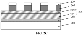
- patterning the first mask layer 207 comprises: depositing a third mask layer 209 on the first mask layer 207; patterning the third mask layer 209 and the first mask layer 207; removing the third mask layer 209 and retaining the first mask layer 207.
- the symmetrical spacer can be formed by one-step etching.
- the third mask layer 209 is deposited on the first mask layer 207.
- the material of the third mask layer may include, but is not limited to, an oxide or silicon oxynitride (SiON), such as, for example, silica (SiO 2 ) or oxygen-enriched silicon oxynitride.
- the process for forming the third mask layer includes, but is not limited to, chemical vapor deposition (CVD), plasma enhanced chemical vapor deposition (PECVD), atomic layer deposition (ALD), or a combination thereof.
- the third mask layer 209 and the first mask layer 207 are patterned.
- patterning the third mask layer 209 and the first mask layer 207 comprises: forming a photoresist (PR) layer on the third mask layer 209; patterning the photoresist layer to form a first patterned photoresist layer 211, the first patterned photoresist layer 211 exposing the third mask layer 209; etching the third mask layer 209 and the first mask layer 207 with the first patterned photoresist layer 211 as a mask.
- a photoresist is spin-coated on the third mask layer 209, and the photoresist is patterned through a mask.
- the process for patterning the third mask layer 209 and the first mask layer 207 is not limited thereto.
- the third mask layer 209 and the first mask layer 207 may also be patterned by self-aligned double patterning (SADP) process or self-aligned quadruple patterning (SAQP) process on the surface of the third mask layer 209.
- SADP self-aligned double patterning
- SAQP self-aligned quadruple patterning
- the third mask layer 209 is removed and the first mask layer 207 is retained.
- the third mask layer 209 may be removed by dry etching that includes sputtering and ion beam milling, plasma etching, high pressure plasma etching, high density plasma (HDP) etching, reactive ion etching (RIE) and the like.
- the photoresist layer further includes a Si-containing anti-reflection coating (SiARC).
- SiARC Si-containing anti-reflection coating
- the anti-reflection coating covers the surface of the third mask layer 209. In this way, the reflected light of lithography can be absorbed, thereby improving the line width resolution in lithography process.
- the operation 103 is performed, that is, spacers 2131 with vertical sidewall morphology are formed on sidewalls of the first mask layer 207.
- the material of the spacers 2131 has a Young's modulus greater than or equal to 25GPa.
- Young's modulus of the material of the spacers 2131 can have a range of 25GPa-250GPa, exemplary, for example, may be 28Gpa, 46Gpa, 190GPa or 230GPa.
- the material of the spacers 2131 comprises polysilicon, silicon nitride or metal oxide.
- the material of the spacers 2131 includes boron-doped polysilicon (Cygnus poly) or titanium oxide. In this way, a higher Young's modulus can be obtained, and the etching selectivity ratio of the material of the spacers to the material of the filling layer material formed subsequently is large, so that the influence on the structure of the filling layer mask is reduced in the subsequent process for removing spacers, and the problem of metal line bridging or breakage is improved.
- forming spacers 2131 with vertical sidewall morphology on sidewalls of the first mask layer 207 comprises: forming a spacer layer 213 covering the first mask layer 207 and a surface of the bottom mask layer 205; removing the spacer layer 213 covering a top of the first mask layer 207 and the spacer layer 213 covering the surface of the bottom mask layer 205, and retaining the spacer layer 213 on the sidewalls of the first mask layer 207 to form spacers 2131 with vertical sidewall morphology.
- the spacer layer 213 covering the first mask layer 207 and a surface of the bottom mask layer 205 is formed.
- the spacer layer may be formed by chemical vapor deposition process, spin coating process, or atomic layer deposition process, and its thickness may have a range of 30nm to 180nm, for example, may be 60nm, 65nm, 80nm, 85nm, 90nm, 95nm, or 120nm. If the thickness of the spacer layer is smaller, it will not be conducive to the subsequent formation of spacers with vertical sidewall morphology, and the spacers with vertical sidewall morphology will easily collapse.
- the thickness of the spacer layer is larger, it will not be conducive to the formation of fine patterns.
- the spacer layer 213 covering the top of the first mask layer 207 and the spacer layer 213 covering the surface of the bottom mask layer 205 is removed, and the spacer layer 213 on the a sidewall of the first mask layer 207 is retained to form spacers 2131 with vertical sidewall morphology.
- the operation 104 is performed, that is the first mask layer 207 is removed.
- the first mask layer 207 may be removed by dry etching process, and the dry etching process includes sputtering and ion beam milling, plasma etching, high pressure plasma etching, high density plasma (HDP) etching, reactive ion etching (RIE) and the like. Dry etching process has high selection ratio, good controllability, flexibility and repeatability, and safe operation of fine lines, which can ensure the high fidelity of fine patterns after transfer.
- removing the first mask layer comprises: removing the first mask layer 207 by an ashing process.
- the pattern of the first mask layer can be efficiently and completely removed by the ashing process, and no intermediate products will be brought.
- the surface cleanliness of the bottom mask layer can be improved, which is beneficial to the subsequent deposition of the filling layer.
- the parameters of the ashing process are as follows. The temperature of the ashing chamber is 235 to 265°C, the radio frequency power is 2000 to 5000W, and the pressure of the ashing chamber is 50 to 1500Mtorr, and the ashing time is 5 to 300 seconds. In this way, the efficiency of removing the first mask layer 207 can be further improved, the cleanliness of the surface of the bottom mask layer can be improved, and the yield is increased.
- smoothing the profile of the spacers is further included such that the profiles of both sides of the spacers are uniformly symmetrically smooth. In this way, the quality of the filling layer mask formed subsequently according to the spacers can be improved, so that the filling layer mask is more regular, thereby improving the yield of the finally formed product.
- the profiles of the spacers are smoothed by the gas etching process, in which the etching gas comprises at least one of Cl 2 , HBr, O 2 , SiCl 4 and SiBr.
- the operation 105 is performed, that is, the gap between the spacers 2131 is filled with a filling layer 215, in which the material of the spacers 2131 to the material of the filling layer 215 has a high etching selectivity ratio.
- filling the gap between the spacers 2131 with the filling layer 215 comprises: forming the filling layer 215 on the bottom mask layer 205, in which the filling layer fills each gap between two adjacent ones of the spacers 2131 and covers the spacers 2131; and planarizing the filling layer 215 such that an upper surface of the filling layer 215 is flush with upper surfaces of the spacers 2131.
- the filling layer 215 is formed on the bottom mask layer 205, in which the filling layer fills the gap between two adjacent ones of the spacers 2131 and covers the spacers2131.
- the material of the filling layer comprises oxide.
- the filling effect of oxide is better, which further solves the problem of poor effect of SOC filling in the prior art.
- the filling layer may be formed by chemical vapor deposition, floating Oxide coating or atomic layer deposition.
- the etching selectivity ratio of the material of the spacers to the material of the filling layer is greater than or equal to 100.
- the etching selectivity ratio of the material of the spacers to the material of the filling layer has, for example, a range of 120-800, and more specifically, may be 155, 334 or 650. In this way, the influence on the filling layer mask structure is reduced in the subsequent process for removing spacers, and the problem of metal line bridging or breakage is improved.
- the filling layer is planarized such that the upper surface of the filling layer 215 is flush with the upper surfaces of the spacers 2131.
- the process of planarization includes chemical mechanical polishing, back etching, or a combination thereof.
- the operation 106 is performed, that is, the spacers 2131 are removed.
- removing the spacers 2131 comprises: removing the spacers 2131 by gas etching, in which the gas comprises chlorine and hydrogen bromide. It should be understood that gas etching has less pollution to the bottom mask, the etching rate is controllable, and the formed filling layer mask is finer. In other embodiments, the gas includes at least one of O 2 , SiCl 4 and SiBr.
- the method further comprises: forming a second mask layer 217 on the filling layer 215; etching the second mask layer 217 to form a second pattern, the second pattern exposing parts of the filling layer 215; patterning the filling layer 215 with the second mask layer as a mask to form a filling layer mask 2151.
- the filling layer is trimmed to form a final mask, which can effectively simplify the process and improve the yield.
- the second mask layer 217 is formed on the filling layer 215.
- the second mask layer 217 may comprise a lower second mask layer 2171 and an upper second mask layer 2172 which are stacked, and the upper second mask layer 2172 is located on the lower second mask layer 2171.
- the material of the upper second mask layer 2172 may include, but is not limited to, silicon oxynitride (SiON), polysilicon (Poly), amorphous carbon layer (ACL), oxide, and the like.
- the upper second mask layer 2172 may be formed by chemical vapor deposition (CVD) or spin-on dielectrics (SOD).
- the material of the lower second mask layer 2171 may include, but is not limited to, a spin-on hard mask (SOH) layer, the SOH layer may be formed by spin coating, and may be an insulating layer of a hydrocarbon system, which may include a silicon hard mask material, a carbon hard mask material, an organic hard mask material, and the like.
- SOH spin-on hard mask
- the second mask layer 217 is etched to form a second pattern, and the second pattern exposes parts of the filling layer 215.
- etching the second mask layer 217 to form a second pattern comprises: forming a photoresist (PR) layer on the second mask layer 217; patterning the photoresist layer to form a second patterned photoresist layer 211', in which the first patterned photoresist layer 211' exposes the second mask layer 217.
- the photoresist layer further includes a Si-containing anti-reflection coating (SiARC) that covers the surface of the second mask layer 217.
- SiARC Si-containing anti-reflection coating
- the process for etching the second mask layer 217 to form the second pattern is not limited thereto.
- the second mask layer 217 may also be etched by self-aligned double patterning (SADP) process or self-aligned quadruple patterning (SAQP) process on the surface of the second mask layer 217 to form the second pattern.
- SADP self-aligned double patterning
- SAQP self-aligned quadruple patterning
- the filling layer 215 is patterned with the second mask layer 217 as a mask to form the filling layer mask 2151.
- the filling layer 215 may be patterned by dry etching that includes sputtering and ion beam milling, plasma etching, high pressure plasma etching, high density plasma (HDP) etching, reactive ion etching (RIE) and the like. Dry etching has a high selection ratio, good controllability, flexibility and repeatability, and safe operation of fine lines, which can ensure the high fidelity of fine patterns after transfer.
- the method further comprises: patterning the bottom mask layer 205 with the filling layer mask 2151 as a mask to form a third pattern, in which the third pattern exposes parts of the etching target layer 203; patterning the etching target layer 203 with the bottom mask layer 205 as a mask.
- the bottom mask layer not only participates in pattern transfer, but also serves as an etching barrier layer to protect the etching target layer and avoid the etching target layer from being damaged by the subsequent process of forming the filling layer mask.
- patterning the bottom mask layer 205 with the filling layer mask 2151 as a mask includes: patterning the bottom mask layer by dry etching.
- dry etching may have etching rates with different speeds, which is first fast and then slow down. This enables a more uniform depth when the desired pattern is subsequently transferred to the bottom mask layer 205.
- the etching rate which is first fast and then slow down, may be achieved by adjusting the pressure of the cavity and/or radio frequency (RF) power of the dry etching device.
- RF radio frequency
- the etching rate increases.
- Increasing RF power can increase the density of active agent and ions in plasma, thereby increasing the etching rate.
- the etching rate, which is first fast and then slow down may be achieved by adjusting the composition of the etching gas and/or the gas flow rate.
- the etching rate can be controlled by adjusting the proportion of composition in the mixed gas.
- the gas flow rate determines the degree of the effective supply of reactant.
- an etching rate which is first fast and then slows down may be achieved by adjusting the etching temperature.
- the etching temperature includes the temperature of the substrate and the temperature of the cavity, and the influence of the temperature is mainly reflected by the chemical reaction rate.
- the bottom mask layer comprises a first bottom mask layer and a second bottom mask layer, and the second bottom mask layer is located on the first bottom mask layer, and the second bottom mask layer has an etching rate greater than the etching rate of the first bottom mask layer.
- the bottom mask layer may include a stack of multiple layers of material with etching rates of each layer gradually decreasing in a top-down direction, thereby achieving the etching rate which is first fast and then slow down using different etching rates of different materials.
- the etching target layer 203 includes an array unit area 20b and a peripheral unit area 20a located on the periphery of the array unit area 20b.
- the spacers 2131 are located on the peripheral unit area 20a.
- Dynamic random access memory includes an array memory cell array and a peripheral circuit.
- the memory cell array and the peripheral circuit may be integrated on the same chip, which allows for a wider bus and higher operating speeds. In practical applications, the memory cell array and the peripheral circuit may be formed in different areas of the same plane. Because the array unit area and the peripheral unit area have different device densities, and are not suitable for one-step formation. Patterning the metal layers separately can effectively improve the yield.
- the bottom mask layer 205 can be used to protect the device in the array unit area 20b, and avoid the contamination of process of patterning the etching target layer in the peripheral unit area 20a.
- the etching target layer 203 in the array unit area 20b is patterned individually firstly and the device in the array unit area 20b is protected by the bottom mask layer 205. Then, for the etching target layer 203 in the peripheral unit area 20a, the method of forming spacers with vertical sidewall morphology, then depositing a filling layer and removing the spacers to form recesses is adopted to form a mask with a corresponding pattern for etching the etching target layer 203 in the peripheral unit area 20a.
- the sequence of separately patterning the etching target layer 203 in the array unit area 20b and the etching target layer 203 in the peripheral unit area 20a described above can be executed in reverse order without conflict.
- Embodiments of the present disclosure also provide a semiconductor structure prepared by anyone of the above methods.
- embodiments of the present disclosure provide a preparation method for a semiconductor structure and a semiconductor structure.
- the preparation method comprises: providing a structure to be processed, in which the structure to be processed comprises a substrate, and an etching target layer, a bottom mask layer and a first mask layer stacked on the substrate; patterning the first mask layer to form a first pattern, the first pattern exposing parts of the bottom mask layer; forming spacers with vertical sidewall morphology on sidewalls of the first mask layer; removing the first mask layer; filling a gap between the spacers with a filling layer, in which a material of the spacers to a material of the filling layer has a high etching selectivity ratio; removing the spacers.
- the embodiments of the present disclosure adopts a method of forming spacers with vertical sidewall morphology firstly, then depositing a filling layer and removing the spacers to form recesses, to form a mask with a corresponding pattern, and a high etching selectivity ratio of the spacers to the filling layer can improve the consistency of pattern transfer and the fineness of forming a patterned structure.
- the embodiments of the present disclosure adopt a method of forming spacers with vertical sidewall morphology firstly, then depositing a filling layer and removing the spacers to form recesses, to form a mask with a corresponding pattern and a high etching selectivity ratio of the spacers to the filling layer can improve the consistency of pattern transfer and the fineness of forming a patterned structure.
Landscapes
- Drying Of Semiconductors (AREA)
Abstract
Description
- This application is based on, and claims priority to
Chinese Patent Application No. 202210209445.5, filed on March. 4, 2022 - The disclosure relates to, but not limited to, the technical field of semiconductor, in particular to a preparation method for a semiconductor structure and a semiconductor structure.
- With the evolution of semiconductor technology nodes and machines, the density of devices in integrated circuits becomes increasingly high, and the feature critical dimensions (CD) of semiconductor devices are decreasing, which has approached the optical physical limit of lithography. The mask patterns formed by existing lithography processes are difficult to meet the requirements of continuously decreasing feature critical dimensions of semiconductor devices, which limits the development of semiconductor technology. How to optimize the preparation process of fine patterns has become an urgent problem to be solved.
- Embodiments of the present disclosure provide a preparation method for a semiconductor structure. The method comprises: providing a structure to be processed, in which the structure to be processed comprises a substrate, and an etching target layer, a bottom mask layer and a first mask layer stacked on the substrate; patterning the first mask layer to form a first pattern, the first pattern exposing parts of the bottom mask layer; forming spacers with vertical sidewall morphology on sidewalls of the first mask layer; removing the first mask layer; filling a gap between the spacers with a filling layer, in which there is a high etching selectivity ratio of a material of the spacers to a material of the filling layer; and removing the spacers.
- In some embodiments, after removing the spacers, the preparation method further comprises: forming a second mask layer on the filling layer; etching the second mask layer to form a second pattern, the second pattern exposing parts of the filling layer; and patterning the filling layer with the second mask layer as a mask to form a filling layer mask.
- In some embodiments, after forming the filling layer mask, the method further comprises: patterning the bottom mask layer with the filling layer mask as a mask to form a third pattern, the third pattern exposing parts of the etching target layer; and patterning the etching target layer with the bottom mask layer as a mask.
- In some embodiments, the etching selectivity ratio of the material of the spacers to the material of the filling layer is greater than or equal to 100.
- In some embodiments, the material of the spacers has a Young's modulus greater than or equal to 25GPa.
- In some embodiments, the material of the filling layer comprises oxide.
- In some embodiments, the material of the spacers comprises polysilicon, silicon nitride or metal oxide.
- In some embodiments, forming spacers with vertical sidewall morphology on sidewalls of the first mask layer comprises: forming a spacer layer covering the first mask layer and a surface of the bottom mask layer; removing the spacer layer covering a top of the first mask layer and the spacer layer covering the surface of the bottom mask layer, and retaining the spacer layer on the sidewalls of the first mask layer to form the spacers with vertical sidewall morphology.
- In some embodiments, removing the spacers comprises: removing the spacers by an etching process with gas, in which the gas comprises chlorine and hydrogen bromide.
- In some embodiments, removing the first mask layer comprises: removing the first mask layer by an ashing process.
- In some embodiments, patterning the first mask layer comprises: depositing a third mask layer on the first mask layer; patterning the third mask layer and the first mask layer; and removing the third mask layer and retaining the first mask layer.
- In some embodiments, patterning the third mask layer and the first mask layer comprises: forming a photoresist layer on the third mask layer; patterning the photoresist layer to form a first patterned photoresist layer, the first patterned photoresist layer exposing the third mask layer; and etching the third mask layer and the first mask layer with the first patterned photoresist layer as a mask.
- In some embodiments, filling the gap between the spacers with the filling layer comprises: forming the filling layer on the bottom mask layer, the filling layer filling the gap between two adjacent ones of the spacers and covering the spacers; planarizing the filling layer such that an upper surface of the filling layer is flush with upper surfaces of the spacers.
- In some embodiments, the bottom mask layer comprises a first bottom mask layer and a second bottom mask layer, and the second bottom mask layer is located on the first bottom mask layer.
- Embodiments of the present disclosure also provide a semiconductor structure prepared by anyone of the above methods.
- Embodiments of the present disclosure provide a preparation method for a semiconductor structure and a semiconductor structure. Herein, the preparation method comprises: providing a structure to be processed, in which the structure to be processed comprises a substrate, and an etching target layer, a bottom mask layer and a first mask layer stacked on the substrate; patterning the first mask layer to form a first pattern, the first pattern exposing parts of the bottom mask layer; forming spacers with vertical sidewall morphology on sidewalls of the first mask layer; removing the first mask layer; filling a gap between the spacers with a filling layer, in which a material of the spacers to a material of the filling layer has a high etching selectivity ratio; removing the spacers. The embodiments of the present disclosure adopt a method of forming spacers with vertical sidewall morphology firstly, then depositing a filling layer and removing the spacers to form recesses, to form a mask with a corresponding pattern, and a high etching selectivity ratio of the spacers to the filling layer can improve the consistency of pattern transfer and the fineness of forming a patterned structure.
- In order to more clearly illustrate the embodiments of the disclosure or the technical solution in the conventional technique, a brief description of the drawings required to be used in the embodiments will be provided below. Apparently, the drawings of the following description are merely some embodiments of the disclosure. For a person of ordinary skill in the art, other drawings can be obtained based on these drawings without creative work.
-
FIG 1 illustrates a flow chart of a preparation method for a semiconductor structure in an embodiment of the present disclosure; -
FIGs 2A to 2N illustrate a device structural diagram of a semiconductor structure provided by embodiments of the present disclosure in the preparing process; -
FIG 3 illustrates a device structural diagram of a semiconductor structure provided by another embodiment of the present disclosure; - 201: substrate; 203: etching target layer; 205: bottom mask layer; 2051: first bottom mask layer; 2052: second bottom mask layer; 207: first mask layer; 209: third mask layer; 211: first patterned photoresist layer; 211': second patterned photoresist layer; 213: spacer layer; 2131: spacer; 215: filling layer; 2151: filling layer mask; 217: second mask layer; 2171: lower second mask layer; 2172: upper second mask layer; 20a: peripheral unit area; 20b: array unit area.
- Exemplary embodiments of the present disclosure will be described in more detail below with reference to the accompanying drawings. Although exemplary embodiments of the present disclosure are shown in the drawings, it should be understood that the present disclosure may be embodied in various forms and should be not be limited to the specific embodiments set forth herein. These embodiments are provided so that the disclosure will be more thoroughly understood and the scope of the disclosure will be fully conveyed to those skilled in the art.
- In the description herein below, numerous specific details are given to provide a more thorough understanding of the disclosure. However it will be apparent to those skilled in the art that the present disclosure may be embodied without one or more of these details. In other examples, some technical features well known in the art are not described in order to avoid confusion with the present disclosure; that is, not all of the features of the actual embodiment are described herein and well-known functions and structures are not described in detail.
- In the drawings, the dimensions of layers, regions, elements and their relative dimensions may be exaggerated for clarity. Throughout the description, the same reference numeral denotes the same element.
- It should be understood that when an element or layer is referred to as "on", "adjacent to", "connected to" or "coupled to" another element or layer, it may be directly on the another element or layer, adjacent to the another element or layer, or connected to or coupled to the another element or layer, or there may be an intermediate element or layer. In contrast, when an element is referred to as "directly on", "directly adjacent to", "directly connected to" or "directly coupled to" another element or layer, there is no intermediate element or layer. It should be understood that although the terms , "first", "second", "third" and the like may be used to describe various elements, components, regions, layers, and/or portions, these elements, components, regions, layers, and/or portions should not be limited by these terms. These terms are only used to distinguish one element, component, region, layer or portion from another element, component, region, layer or portion. Therefore, without departing from the teaching of the present disclosure, a first element, component, region, layer or portion discussed hereinafter may be expressed as a second element, component, region, layer or portion. While discussing a second element, component, region, layer or portion, it does not imply that a first element, component, region, layer or portion is necessarily present in the present disclosure.
- The terms used herein are intended to describe specific embodiments only and are not to be a limitation to the present disclosure. As used herein, the singular forms "a/an", "one", and "the" may include the plural forms as well, unless the context clearly dictates otherwise. It should be further understood that when terms "comprise " and/or "include" are used in the specification, it means that the stated features, integers, steps, operations, elements and/or components are present, but the presence or addition of one or more of other features, integers, steps, operations, elements, components and/or combinations is not excluded. When used herein, the term "and/or" includes any of the listed items and all combinations thereof.
- Patterning process in related art is prone to problems such as bridge, breakage, poor filling quality in corner space, etc., and it is often difficult to form a fine patterned structure.
- On the basis of this, embodiments of the present disclosure provide a preparation method for a semiconductor structure. With reference to
FIG 1 , the preparation method comprises the following operations. - The operation 101: A structure to be processed is provided, in which the structure to be processed comprises a substrate, an etching target layer, a bottom mask layer and a first mask layer stacked on the substrate.
- The operation 102: The first mask layer is patterned to form a first pattern, in which the first pattern exposes parts of the bottom mask layer.
- The operation 103: Spacers with vertical sidewall morphology are formed on sidewalls of the first mask layer.
- The operation 104: The first mask layer is removed.
- The operation 105: A gap between the spacers is filled with a filling layer, in which a material of the spacers to a material of the filling layer has a high etching selectivity ratio.
- The operation 105: The spacers are removed.
- The embodiments of the present disclosure adopt a method of forming spacers with vertical sidewall morphology firstly, then depositing a filling layer and removing the spacers to form a recess, to form a mask corresponding to a pattern. The high etching selectivity ratio of the spacers to the filling layer can improve the consistency of pattern transfer and the fineness of forming a patterned structure.
- Specific embodiments of the present disclosure will be described in detail below with reference to
FIGs 2A to 2N . In detailing the embodiments of the present disclosure, the schematic diagram is partially enlarged without a general scale for convenience in description, and the schematic diagram is only taken as an example, which should not limit the scope of protection of the disclosure herein. - The method begins with the
operation 101, as shown inFIG 2A , a structure to be processed is provided, in which the structure to be processed includes asubstrate 201, and anetching target layer 203, abottom mask layer 205 and afirst mask layer 207 stacked on the substrate. - Here, the substrate may be a semiconductor substrate and may include at least one elemental semiconductor material (e.g. silicon (Si) substrate, germanium (Ge) substrate), at least one III-V compound semiconductor material, at least one II-VI compound semiconductor material, at least one organic semiconductor material, or other semiconductor materials known in the art. In a specific embodiment, the substrate is a silicon substrate, which may be doped or undoped. Specifically, the substrate may be, but is not limited to, a wafer.
- Taking as an example, the
etching target layer 203 may be a material layer to be etched, which is located on a substrate, for instance, including but not limited to a polysilicon layer or a metal layer, and in some embodiments may also be a substrate; that is, the target layer to be etched later may be a polysilicon layer located on the base, also may be a metal layer located on the substrate or may be the substrate itself. In some embodiments, theetching target layer 203 may be tungsten (W). - In some embodiments, with reference to
FIG 2A , thebottom mask layer 205 comprises a firstbottom mask layer 2051 and a secondbottom mask layer 2052, and the secondbottom mask layer 2052 is located above the firstbottom mask layer 2051. Herein, thebottom mask layer 205 not only participates in pattern transfer, but also serves as an etching barrier layer to protect the etching target layer and avoid the etching target layer from being damaged by the subsequent process of forming a filling layer mask. The mask layer with multi-layer structure can improve the line width consistency and edge roughness. Here, the material of the firstbottom mask layer 2051 may include, but is not limited to, an amorphous carbon layer (ACL), and the material of the secondbottom mask layer 2052 may include, but is not limited to, silicon nitride (SiN) or silicon oxynitride (SiON). More specifically, the material of the second bottom mask layer may be silicon-rich silicon oxynitride. In practice, the process for forming thebottom mask layer 205 includes, but is not limited to, chemical vapor deposition (CVD), plasma enhanced chemical vapor deposition (PECVD), atomic layer deposition (ALD), or a combination thereof. - Here, the
first mask layer 207 may include but is not limited to an amorphous carbon layer (ACL). In practice, the forming process of thefirst mask layer 207 includes, but is not limited to, chemical vapor deposition (CVD), plasma enhanced chemical vapor deposition (PECVD), atomic layer deposition (ALD), or a combination thereof. - Subsequently, as shown in
FIGs. 2B to 2D , theoperation 102 is performed, that is, thefirst mask layer 207 is patterned to form a first pattern, in which the first pattern exposes parts of thebottom mask layer 205. - In some embodiments, as shown in
FIGs.2B to 2D , patterning thefirst mask layer 207 comprises: depositing athird mask layer 209 on thefirst mask layer 207; patterning thethird mask layer 209 and thefirst mask layer 207; removing thethird mask layer 209 and retaining thefirst mask layer 207. In this way, after the cap layer structure at the top is removed and then the spacer layer with high modulus is deposited, the symmetrical spacer can be formed by one-step etching. - Specifically, firstly, referring to
FIG 2B , thethird mask layer 209 is deposited on thefirst mask layer 207. Here, the material of the third mask layer may include, but is not limited to, an oxide or silicon oxynitride (SiON), such as, for example, silica (SiO2) or oxygen-enriched silicon oxynitride. In practice, the process for forming the third mask layer includes, but is not limited to, chemical vapor deposition (CVD), plasma enhanced chemical vapor deposition (PECVD), atomic layer deposition (ALD), or a combination thereof. - Subsequently, referring to
FIG2C , thethird mask layer 209 and thefirst mask layer 207 are patterned. - In some embodiments, patterning the
third mask layer 209 and thefirst mask layer 207 comprises: forming a photoresist (PR) layer on thethird mask layer 209; patterning the photoresist layer to form a firstpatterned photoresist layer 211, the firstpatterned photoresist layer 211 exposing thethird mask layer 209; etching thethird mask layer 209 and thefirst mask layer 207 with the firstpatterned photoresist layer 211 as a mask. For example, a photoresist is spin-coated on thethird mask layer 209, and the photoresist is patterned through a mask. The process for patterning thethird mask layer 209 and thefirst mask layer 207 is not limited thereto. In other embodiments, thethird mask layer 209 and thefirst mask layer 207 may also be patterned by self-aligned double patterning (SADP) process or self-aligned quadruple patterning (SAQP) process on the surface of thethird mask layer 209. - Finally, referring to
FIG2D , thethird mask layer 209 is removed and thefirst mask layer 207 is retained. Here, thethird mask layer 209 may be removed by dry etching that includes sputtering and ion beam milling, plasma etching, high pressure plasma etching, high density plasma (HDP) etching, reactive ion etching (RIE) and the like. - In some embodiments, the photoresist layer further includes a Si-containing anti-reflection coating (SiARC). The anti-reflection coating covers the surface of the
third mask layer 209. In this way, the reflected light of lithography can be absorbed, thereby improving the line width resolution in lithography process. - Subsequently, as shown in
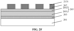
FIG 2F , theoperation 103 is performed, that is,spacers 2131 with vertical sidewall morphology are formed on sidewalls of thefirst mask layer 207. - In some embodiments, the material of the
spacers 2131 has a Young's modulus greater than or equal to 25GPa. In practice, Young's modulus of the material of thespacers 2131 can have a range of 25GPa-250GPa, exemplary, for example, may be 28Gpa, 46Gpa, 190GPa or 230GPa. By choosing the spacers with appropriate Young's modulus, after the pattern of the first mask layer is subsequently removed, it is easier to maintain the vertical morphology for the spacers with high Young's modulus; in addition, the higher the Young's modulus, the less easily the spacers are to deform, so that a finer pattern can be obtained and the accuracy can be improved. In some embodiments, the material of thespacers 2131 has a Young's modulus of less than 500Gpa, so that the spacers and other materials are not prone to delamination caused by stress and have better compatibility. - In some embodiments, the material of the
spacers 2131 comprises polysilicon, silicon nitride or metal oxide. In a specific embodiment, the material of thespacers 2131 includes boron-doped polysilicon (Cygnus poly) or titanium oxide. In this way, a higher Young's modulus can be obtained, and the etching selectivity ratio of the material of the spacers to the material of the filling layer material formed subsequently is large, so that the influence on the structure of the filling layer mask is reduced in the subsequent process for removing spacers, and the problem of metal line bridging or breakage is improved. - In some embodiments, as shown in
FIGs. 2E to 2F , formingspacers 2131 with vertical sidewall morphology on sidewalls of thefirst mask layer 207 comprises: forming aspacer layer 213 covering thefirst mask layer 207 and a surface of thebottom mask layer 205; removing thespacer layer 213 covering a top of thefirst mask layer 207 and thespacer layer 213 covering the surface of thebottom mask layer 205, and retaining thespacer layer 213 on the sidewalls of thefirst mask layer 207 to formspacers 2131 with vertical sidewall morphology. - Specifically, firstly, referring to
FIG 2E , thespacer layer 213 covering thefirst mask layer 207 and a surface of thebottom mask layer 205 is formed. Here, the spacer layer may be formed by chemical vapor deposition process, spin coating process, or atomic layer deposition process, and its thickness may have a range of 30nm to 180nm, for example, may be 60nm, 65nm, 80nm, 85nm, 90nm, 95nm, or 120nm. If the thickness of the spacer layer is smaller, it will not be conducive to the subsequent formation of spacers with vertical sidewall morphology, and the spacers with vertical sidewall morphology will easily collapse. If the thickness of the spacer layer is larger, it will not be conducive to the formation of fine patterns. In practice, when selecting the thickness of the spacer layer, it should take into account the material of the spacers and the Young's modulus of the material of the spacers. For example, if the Young's modulus of the spacer higher, a smaller thickness of the spacer layer may be selected, and thus the fineness of the pattern is improved. - Subsequently, as shown in
FIG 2F , thespacer layer 213 covering the top of thefirst mask layer 207 and thespacer layer 213 covering the surface of thebottom mask layer 205 is removed, and thespacer layer 213 on the a sidewall of thefirst mask layer 207 is retained to formspacers 2131 with vertical sidewall morphology. - Then, as shown in
FIG 2G , theoperation 104 is performed, that is thefirst mask layer 207 is removed. In practice, thefirst mask layer 207 may be removed by dry etching process, and the dry etching process includes sputtering and ion beam milling, plasma etching, high pressure plasma etching, high density plasma (HDP) etching, reactive ion etching (RIE) and the like. Dry etching process has high selection ratio, good controllability, flexibility and repeatability, and safe operation of fine lines, which can ensure the high fidelity of fine patterns after transfer. - In some embodiments, removing the first mask layer comprises: removing the
first mask layer 207 by an ashing process. The pattern of the first mask layer can be efficiently and completely removed by the ashing process, and no intermediate products will be brought. At the same time, the surface cleanliness of the bottom mask layer can be improved, which is beneficial to the subsequent deposition of the filling layer. In practice, the parameters of the ashing process are as follows. The temperature of the ashing chamber is 235 to 265°C, the radio frequency power is 2000 to 5000W, and the pressure of the ashing chamber is 50 to 1500Mtorr, and the ashing time is 5 to 300 seconds. In this way, the efficiency of removing thefirst mask layer 207 can be further improved, the cleanliness of the surface of the bottom mask layer can be improved, and the yield is increased. - In some embodiments, after the pattern of the first mask layer is removed, smoothing the profile of the spacers is further included such that the profiles of both sides of the spacers are uniformly symmetrically smooth. In this way, the quality of the filling layer mask formed subsequently according to the spacers can be improved, so that the filling layer mask is more regular, thereby improving the yield of the finally formed product. In some embodiments, the profiles of the spacers are smoothed by the gas etching process, in which the etching gas comprises at least one of Cl2, HBr, O2, SiCl4 and SiBr.
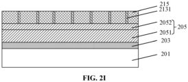
- Subsequently, as shown in
FIG 2I , theoperation 105 is performed, that is, the gap between thespacers 2131 is filled with afilling layer 215, in which the material of thespacers 2131 to the material of thefilling layer 215 has a high etching selectivity ratio. - In some embodiments, as shown in
FIG 2H to 2I , filling the gap between thespacers 2131 with thefilling layer 215 comprises: forming thefilling layer 215 on thebottom mask layer 205, in which the filling layer fills each gap between two adjacent ones of thespacers 2131 and covers thespacers 2131; and planarizing thefilling layer 215 such that an upper surface of thefilling layer 215 is flush with upper surfaces of thespacers 2131. - Specifically, firstly, referring to
FIG2H , thefilling layer 215 is formed on thebottom mask layer 205, in which the filling layer fills the gap between two adjacent ones of thespacers 2131 and covers the spacers2131. In some embodiments, the material of the filling layer comprises oxide. Compared with spin-on-carbon (SOC) layer filled by the related technology, the filling effect of oxide is better, which further solves the problem of poor effect of SOC filling in the prior art. In practice, the filling layer may be formed by chemical vapor deposition, floating Oxide coating or atomic layer deposition. - In some embodiments, the etching selectivity ratio of the material of the spacers to the material of the filling layer is greater than or equal to 100. Exemplary, the etching selectivity ratio of the material of the spacers to the material of the filling layer has, for example, a range of 120-800, and more specifically, may be 155, 334 or 650. In this way, the influence on the filling layer mask structure is reduced in the subsequent process for removing spacers, and the problem of metal line bridging or breakage is improved.
- Subsequently, referring to
FIG 2I , the filling layer is planarized such that the upper surface of thefilling layer 215 is flush with the upper surfaces of thespacers 2131. In practice, the process of planarization includes chemical mechanical polishing, back etching, or a combination thereof. - Finally, referring to
FIG 2J , the operation 106 is performed, that is, thespacers 2131 are removed. - In some embodiments, removing the
spacers 2131 comprises: removing thespacers 2131 by gas etching, in which the gas comprises chlorine and hydrogen bromide. It should be understood that gas etching has less pollution to the bottom mask, the etching rate is controllable, and the formed filling layer mask is finer. In other embodiments, the gas includes at least one of O2, SiCl4 and SiBr. - In some embodiments, as shown in
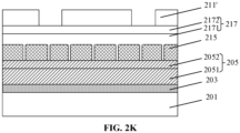
FIG 2K to 2M , after removing thespacers 2131, the method further comprises: forming asecond mask layer 217 on thefilling layer 215; etching thesecond mask layer 217 to form a second pattern, the second pattern exposing parts of thefilling layer 215; patterning thefilling layer 215 with the second mask layer as a mask to form afilling layer mask 2151. In practice, because of the precision and complex of the pattern, the process of one-step etching is difficult, and the process maintenance is difficult or even impossible to achieve. In this way, the filling layer is trimmed to form a final mask, which can effectively simplify the process and improve the yield. - Specifically, firstly, referring to
FIG 2K , thesecond mask layer 217 is formed on thefilling layer 215. Here, thesecond mask layer 217 may comprise a lowersecond mask layer 2171 and an uppersecond mask layer 2172 which are stacked, and the uppersecond mask layer 2172 is located on the lowersecond mask layer 2171. The material of the uppersecond mask layer 2172 may include, but is not limited to, silicon oxynitride (SiON), polysilicon (Poly), amorphous carbon layer (ACL), oxide, and the like. The uppersecond mask layer 2172 may be formed by chemical vapor deposition (CVD) or spin-on dielectrics (SOD). - The material of the lower
second mask layer 2171 may include, but is not limited to, a spin-on hard mask (SOH) layer, the SOH layer may be formed by spin coating, and may be an insulating layer of a hydrocarbon system, which may include a silicon hard mask material, a carbon hard mask material, an organic hard mask material, and the like. - Subsequently, referring to
FIG 2I , thesecond mask layer 217 is etched to form a second pattern, and the second pattern exposes parts of thefilling layer 215. In some embodiments, etching thesecond mask layer 217 to form a second pattern comprises: forming a photoresist (PR) layer on thesecond mask layer 217; patterning the photoresist layer to form a second patterned photoresist layer 211', in which the first patterned photoresist layer 211' exposes thesecond mask layer 217. In some embodiments, the photoresist layer further includes a Si-containing anti-reflection coating (SiARC) that covers the surface of thesecond mask layer 217. In this way, the reflected light of lithography can be absorbed, thereby improving the linewidth resolution in lithography process. The process for etching thesecond mask layer 217 to form the second pattern is not limited thereto. In other embodiments, thesecond mask layer 217 may also be etched by self-aligned double patterning (SADP) process or self-aligned quadruple patterning (SAQP) process on the surface of thesecond mask layer 217 to form the second pattern. - Finally, referring to
FIG2M , thefilling layer 215 is patterned with thesecond mask layer 217 as a mask to form thefilling layer mask 2151. Here, thefilling layer 215 may be patterned by dry etching that includes sputtering and ion beam milling, plasma etching, high pressure plasma etching, high density plasma (HDP) etching, reactive ion etching (RIE) and the like. Dry etching has a high selection ratio, good controllability, flexibility and repeatability, and safe operation of fine lines, which can ensure the high fidelity of fine patterns after transfer. - In some embodiments, as shown in
FIG2N , after forming thefilling layer mask 2151, the method further comprises: patterning thebottom mask layer 205 with thefilling layer mask 2151 as a mask to form a third pattern, in which the third pattern exposes parts of theetching target layer 203; patterning theetching target layer 203 with thebottom mask layer 205 as a mask. Here, the bottom mask layer not only participates in pattern transfer, but also serves as an etching barrier layer to protect the etching target layer and avoid the etching target layer from being damaged by the subsequent process of forming the filling layer mask. - In one embodiment, patterning the
bottom mask layer 205 with thefilling layer mask 2151 as a mask includes: patterning the bottom mask layer by dry etching. In some embodiments, dry etching may have etching rates with different speeds, which is first fast and then slow down. This enables a more uniform depth when the desired pattern is subsequently transferred to thebottom mask layer 205. - In some embodiments, the etching rate, which is first fast and then slow down, may be achieved by adjusting the pressure of the cavity and/or radio frequency (RF) power of the dry etching device. Generally, with the increase of cavity pressure, the etching rate increases. Increasing RF power can increase the density of active agent and ions in plasma, thereby increasing the etching rate. In other embodiments, the etching rate, which is first fast and then slow down, may be achieved by adjusting the composition of the etching gas and/or the gas flow rate. For example, the etching rate can be controlled by adjusting the proportion of composition in the mixed gas. On the other hand, the gas flow rate determines the degree of the effective supply of reactant. If gas flow rate is too low, the etching rate is limited by the supplement of reactant gas, which will reduce the etching rate. If the gas flow rate is too high, it will lead to the loss of reactant gas in transit, which will also reduce the etching rate. In other embodiments, an etching rate which is first fast and then slows down may be achieved by adjusting the etching temperature. The etching temperature includes the temperature of the substrate and the temperature of the cavity, and the influence of the temperature is mainly reflected by the chemical reaction rate.
- In other embodiments, the bottom mask layer comprises a first bottom mask layer and a second bottom mask layer, and the second bottom mask layer is located on the first bottom mask layer, and the second bottom mask layer has an etching rate greater than the etching rate of the first bottom mask layer. In some other embodiments, the bottom mask layer may include a stack of multiple layers of material with etching rates of each layer gradually decreasing in a top-down direction, thereby achieving the etching rate which is first fast and then slow down using different etching rates of different materials.
- In some embodiments, as shown in
FIG 3 theetching target layer 203 includes anarray unit area 20b and aperipheral unit area 20a located on the periphery of thearray unit area 20b. Thespacers 2131 are located on theperipheral unit area 20a. Dynamic random access memory (DRAM) includes an array memory cell array and a peripheral circuit. The memory cell array and the peripheral circuit may be integrated on the same chip, which allows for a wider bus and higher operating speeds. In practical applications, the memory cell array and the peripheral circuit may be formed in different areas of the same plane. Because the array unit area and the peripheral unit area have different device densities, and are not suitable for one-step formation. Patterning the metal layers separately can effectively improve the yield. At this time, thebottom mask layer 205 can be used to protect the device in thearray unit area 20b, and avoid the contamination of process of patterning the etching target layer in theperipheral unit area 20a. Referring toFIG 3 , theetching target layer 203 in thearray unit area 20b is patterned individually firstly and the device in thearray unit area 20b is protected by thebottom mask layer 205. Then, for theetching target layer 203 in theperipheral unit area 20a, the method of forming spacers with vertical sidewall morphology, then depositing a filling layer and removing the spacers to form recesses is adopted to form a mask with a corresponding pattern for etching theetching target layer 203 in theperipheral unit area 20a. In this way, the process difficulty can be effectively reduced, the complexity of the pattern is reduced, and the yield is improved. It should be understood that, the sequence of separately patterning theetching target layer 203 in thearray unit area 20b and theetching target layer 203 in theperipheral unit area 20a described above can be executed in reverse order without conflict. - Embodiments of the present disclosure also provide a semiconductor structure prepared by anyone of the above methods.
- In summary, embodiments of the present disclosure provide a preparation method for a semiconductor structure and a semiconductor structure. Herein, the preparation method comprises: providing a structure to be processed, in which the structure to be processed comprises a substrate, and an etching target layer, a bottom mask layer and a first mask layer stacked on the substrate; patterning the first mask layer to form a first pattern, the first pattern exposing parts of the bottom mask layer; forming spacers with vertical sidewall morphology on sidewalls of the first mask layer; removing the first mask layer; filling a gap between the spacers with a filling layer, in which a material of the spacers to a material of the filling layer has a high etching selectivity ratio; removing the spacers. The embodiments of the present disclosure adopts a method of forming spacers with vertical sidewall morphology firstly, then depositing a filling layer and removing the spacers to form recesses, to form a mask with a corresponding pattern, and a high etching selectivity ratio of the spacers to the filling layer can improve the consistency of pattern transfer and the fineness of forming a patterned structure.
- In should be noted that the preparation method for a semiconductor structure and the semiconductor structure provided by the embodiments of the present disclosure may be applied to any integrated circuit including this structure. Any technical feature of the technical solution described in each embodiment can be arbitrarily combined without conflict. Those skilled in the art can change the operation sequence of the formation method without leaving the protection scope of the present disclosure. Under the condition that each operation of the embodiments of the present disclosure does not conflict, part of the operations may be executed at the same time or may be executed in reverse order.
- The descriptions above are only preferred embodiments of the present disclosure, and are not intended to limit the scope of protection of the present disclosure. Any modification, equivalent replacement and improvement made within the spirit and principles of the present disclosure all fall with the protection scope of the present disclosure.
- The embodiments of the present disclosure adopt a method of forming spacers with vertical sidewall morphology firstly, then depositing a filling layer and removing the spacers to form recesses, to form a mask with a corresponding pattern and a high etching selectivity ratio of the spacers to the filling layer can improve the consistency of pattern transfer and the fineness of forming a patterned structure.
Claims (15)
- A preparation method for a semiconductor structure, comprising:providing a structure to be processed, wherein the structure to be processed comprises a substrate, and an etching target layer, a bottom mask layer and a first mask layer stacked on the substrate;patterning the first mask layer to form a first pattern, the first pattern exposing parts of the bottom mask layer;forming spacers with vertical sidewall morphology on sidewalls of the first mask layer;removing the first mask layer;filling a gap between the spacers with a filling layer,wherein there is a high etching selectivity ratio of a material of the spacers to a material of the filling layer; andremoving the spacers.
- The preparation method according to claim 1, wherein, after removing the spacers, the preparation method further comprises:forming a second mask layer on the filling layer;etching the second mask layer to form a second pattern, the second pattern exposing parts of the filling layer; andpatterning the filling layer with the second mask layer as a mask to form a filling layer mask.
- The preparation method according to claim 2, wherein, after forming the filling layer mask, the method further comprises:patterning the bottom mask layer with the filling layer mask as a mask to form a third pattern, the third pattern exposing parts of the etching target layer; andpatterning the etching target layer with the bottom mask layer as a mask.
- The preparation method according to claim 1, wherein, the etching selectivity ratio of the material of the spacers to the material of the filling layer is greater than or equal to 100.
- The preparation method according to claim 1, wherein, the material of the spacers has a Young's modulus greater than or equal to 25GPa.
- The preparation method according to claim 1, wherein, the material of the filling layers comprises oxide.
- The preparation method according to claim 1, wherein, the material of the spacers comprises polysilicon, silicon nitride or metal oxide.
- The preparation method according to claim 1, wherein, forming spacers with vertical sidewall morphology on sidewalls of the first mask layer comprises:forming a spacer layer covering the first mask layer and a surface of the bottom mask layer; andremoving the spacer layer covering a top of the first mask layer and the spacer layer covering the surface of the bottom mask layer, and retaining the spacer layer on the sidewalls of the first mask layer to form the spacers with vertical sidewall morphology.
- The preparation method according to claim 1, wherein, removing the spacers comprises:removing the spacers by an etching process with gas, wherein the gas comprises chlorine and hydrogen bromide.
- The preparation method according to claim 1, wherein, removing the first mask layer comprises:
removing the first mask layer by an ashing process. - The preparation method according to claim 1, wherein, patterning the first mask layer comprises:depositing a third mask layer on the first mask layer;patterning the third mask layer and the first mask layer; andremoving the third mask layer and retaining the first mask layer.
- The preparation method according to claim 11, wherein, patterning the third mask layer and the first mask layer comprises:forming a photoresist layer on the third mask layer;patterning the photoresist layer to form a first patterned photoresist layer, the first patterned photoresist layer exposing the third mask layer; andetching the third mask layer and the first mask layer with the first patterned photoresist layer as a mask.
- The preparation method according to claim 1, wherein, filling the gap between the spacers with the filling layer comprises:forming the filling layer on the bottom mask layer, the filling layer filling the gap between two adjacent ones of the spacers and covering the spacers; andplanarizing the filling layer such that an upper surface of the filling layer is flush with upper surfaces of the spacers.
- The preparation method according to claim 1, wherein,
the bottom mask layer comprises a first bottom mask layer and a second bottom mask layer, and the second bottom mask layer is located on the first bottom mask layer. - A semiconductor structure prepared by the preparation method for a semiconductor structure according to anyone of claims 1 to 14.
Applications Claiming Priority (2)
| Application Number | Priority Date | Filing Date | Title |
|---|---|---|---|
| CN202210209445.5A CN116741626A (en) | 2022-03-04 | 2022-03-04 | Preparation method of semiconductor structure and semiconductor structure |
| PCT/CN2022/080318 WO2023164966A1 (en) | 2022-03-04 | 2022-03-11 | Method for preparing semiconductor structure, and semiconductor structure |
Publications (2)
| Publication Number | Publication Date |
|---|---|
| EP4261869A1 true EP4261869A1 (en) | 2023-10-18 |
| EP4261869A4 EP4261869A4 (en) | 2023-11-15 |
Family
ID=84044748
Family Applications (1)
| Application Number | Title | Priority Date | Filing Date |
|---|---|---|---|
| EP22728335.5A Withdrawn EP4261869A4 (en) | 2022-03-04 | 2022-03-11 | METHOD FOR PREPARING SEMICONDUCTOR STRUCTURE, AND SEMICONDUCTOR STRUCTURE |
Country Status (7)
| Country | Link |
|---|---|
| US (1) | US12341010B2 (en) |
| EP (1) | EP4261869A4 (en) |
| JP (1) | JP7527382B2 (en) |
| KR (1) | KR102775089B1 (en) |
| CN (1) | CN116741626A (en) |
| TW (1) | TWI829194B (en) |
| WO (1) | WO2023164966A1 (en) |
Family Cites Families (30)
| Publication number | Priority date | Publication date | Assignee | Title |
|---|---|---|---|---|
| JP4686006B2 (en) | 2000-04-27 | 2011-05-18 | 大日本印刷株式会社 | Halftone phase shift photomask, blank for halftone phase shift photomask, and method for manufacturing halftone phase shift photomask |
| US6429123B1 (en) * | 2000-10-04 | 2002-08-06 | Vanguard International Semiconductor Corporation | Method of manufacturing buried metal lines having ultra fine features |
| JP4193438B2 (en) * | 2002-07-30 | 2008-12-10 | ソニー株式会社 | Manufacturing method of semiconductor device |
| TWI237871B (en) * | 2003-11-17 | 2005-08-11 | Nanya Technology Corp | Method of forming contacts for memory device |
| US20060199370A1 (en) * | 2005-03-01 | 2006-09-07 | Taiwan Semiconductor Manufacturing Co., Ltd. | Method of in-situ ash strip to eliminate memory effect and reduce wafer damage |
| US7291560B2 (en) | 2005-08-01 | 2007-11-06 | Infineon Technologies Ag | Method of production pitch fractionizations in semiconductor technology |
| KR100876808B1 (en) * | 2006-07-10 | 2009-01-07 | 주식회사 하이닉스반도체 | Pattern formation method of semiconductor device |
| US8227352B2 (en) | 2010-04-30 | 2012-07-24 | Applied Materials, Inc. | Amorphous carbon deposition method for improved stack defectivity |
| KR101804517B1 (en) * | 2011-06-01 | 2018-01-10 | 삼성전자 주식회사 | Method for fabricating metal contact using DPT(Double Patterning Technology) |
| US8916337B2 (en) * | 2012-02-22 | 2014-12-23 | International Business Machines Corporation | Dual hard mask lithography process |
| US20150035064A1 (en) | 2013-08-01 | 2015-02-05 | International Business Machines Corporation | Inverse side-wall image transfer |
| US8987008B2 (en) | 2013-08-20 | 2015-03-24 | Taiwan Semiconductor Manufacturing Company, Ltd. | Integrated circuit layout and method with double patterning |
| US8969206B1 (en) * | 2013-09-04 | 2015-03-03 | Sandisk Technologies Inc. | Triple patterning NAND flash memory with stepped mandrel |
| US9595441B2 (en) | 2014-12-22 | 2017-03-14 | Tokyo Electron Limited | Patterning a substrate using grafting polymer material |
| JP6604738B2 (en) * | 2015-04-10 | 2019-11-13 | 東京エレクトロン株式会社 | Plasma etching method, pattern forming method, and cleaning method |
| CN106252229B (en) * | 2015-06-12 | 2019-04-23 | 中国科学院微电子研究所 | A method of manufacturing a semiconductor device |
| US9911619B1 (en) * | 2016-10-12 | 2018-03-06 | Globalfoundries Inc. | Fin cut with alternating two color fin hardmask |
| US10157751B1 (en) * | 2017-10-26 | 2018-12-18 | Taiwan Semiconductor Manufacturing Co., Ltd. | Method for manufacturing semiconductor device |
| US10991584B2 (en) | 2017-12-19 | 2021-04-27 | International Business Machines Corporation | Methods and structures for cutting lines or spaces in a tight pitch structure |
| US10181401B1 (en) * | 2018-01-08 | 2019-01-15 | Nanya Technology Corporation | Method for manufacturing a semiconductor device |
| US10629437B2 (en) * | 2018-05-09 | 2020-04-21 | Varian Semiconductor Equipment Associates, Inc. | Techniques and structure for forming dynamic random-access device using angled ions |
| US10867804B2 (en) | 2018-06-29 | 2020-12-15 | Taiwan Semiconductor Manufacturing Company, Ltd. | Patterning method for semiconductor device and structures resulting therefrom |
| US11393694B2 (en) | 2018-11-13 | 2022-07-19 | Tokyo Electron Limited | Method for planarization of organic films |
| US11676821B2 (en) * | 2019-10-29 | 2023-06-13 | Taiwan Semiconductor Manufacturing Co., Ltd. | Self-aligned double patterning |
| CN110993499B (en) * | 2019-11-05 | 2022-08-16 | 北京北方华创微电子装备有限公司 | Etching method, air gap type dielectric layer and dynamic random access memory |
| US11315786B2 (en) | 2020-03-06 | 2022-04-26 | Nanya Technology Corporation | Semiconductor device structure with fine patterns at different levels and method for forming the same |
| TWI724815B (en) | 2020-03-10 | 2021-04-11 | 華邦電子股份有限公司 | Method for forming semiconductor structure |
| KR20220162158A (en) | 2020-04-30 | 2022-12-07 | 후지필름 가부시키가이샤 | Structure manufacturing method, and structure |
| CN111584431B (en) | 2020-05-19 | 2023-06-02 | 上海集成电路研发中心有限公司 | A self-aligned quadruple pattern forming method |
| US11776812B2 (en) * | 2020-05-22 | 2023-10-03 | Tokyo Electron Limited | Method for pattern reduction using a staircase spacer |
-
2022
- 2022-03-04 CN CN202210209445.5A patent/CN116741626A/en active Pending
- 2022-03-11 JP JP2022548078A patent/JP7527382B2/en active Active
- 2022-03-11 KR KR1020227026579A patent/KR102775089B1/en active Active
- 2022-03-11 EP EP22728335.5A patent/EP4261869A4/en not_active Withdrawn
- 2022-03-11 WO PCT/CN2022/080318 patent/WO2023164966A1/en not_active Ceased
- 2022-05-13 US US17/743,560 patent/US12341010B2/en active Active
- 2022-06-10 TW TW111121592A patent/TWI829194B/en active
Also Published As
| Publication number | Publication date |
|---|---|
| JP2024512830A (en) | 2024-03-21 |
| TWI829194B (en) | 2024-01-11 |
| TW202336527A (en) | 2023-09-16 |
| CN116741626A (en) | 2023-09-12 |
| KR102775089B1 (en) | 2025-02-27 |
| EP4261869A4 (en) | 2023-11-15 |
| US12341010B2 (en) | 2025-06-24 |
| US20230282479A1 (en) | 2023-09-07 |
| WO2023164966A1 (en) | 2023-09-07 |
| KR20230131101A (en) | 2023-09-12 |
| JP7527382B2 (en) | 2024-08-02 |
Similar Documents
| Publication | Publication Date | Title |
|---|---|---|
| US20220262626A1 (en) | Methods of forming electronic devices using pitch reduction | |
| KR102332866B1 (en) | Patterning methods for semiconductor devices and structures resulting therefrom | |
| US10510540B2 (en) | Mask scheme for cut pattern flow with enlarged EPE window | |
| US8889560B2 (en) | Methods of forming fine patterns for semiconductor device | |
| US10692728B2 (en) | Use of selective aluminum oxide etch | |
| KR20110102872A (en) | Multiple depth shallow trench isolation process | |
| US10957550B2 (en) | Semiconductor structure and formation method thereof | |
| KR100596834B1 (en) | Polysilicon Plug Formation Method of Semiconductor Device | |
| US12341010B2 (en) | Preparation method for semiconductor structure and same | |
| US20220293608A1 (en) | Semiconductor structure having buried word lines and method of manufacturing the same | |
| CN114446788A (en) | Method of forming a semiconductor structure | |
| US12322597B2 (en) | Pitch scaling in microfabrication | |
| US20040031994A1 (en) | Semiconductor device with gate space of positive slope and fabrication method thereof | |
| CN223487039U (en) | semiconductor devices | |
| CN118870807B (en) | Method for preparing semiconductor structure | |
| KR20080084293A (en) | Manufacturing method of semiconductor device | |
| KR20110047820A (en) | Method for manufacturing semiconductor device using hard mask film in which organic film and oxide film are laminated | |
| KR20090027431A (en) | Method of forming fine pattern of semiconductor device | |
| KR100417195B1 (en) | Fabricating method of semiconductor device | |
| KR100695417B1 (en) | Semiconductor device manufacturing method capable of forming a fine pattern | |
| KR20020089998A (en) | Method for Forming ILD in Semiconductor Device | |
| CN105336676A (en) | Forming method of contact plug | |
| CN116417405A (en) | Formation method of semiconductor structure | |
| KR20010004893A (en) | Method of manufacture semiconductor device | |
| KR20090067508A (en) | Method of forming fine pattern of semiconductor device |
Legal Events
| Date | Code | Title | Description |
|---|---|---|---|
| STAA | Information on the status of an ep patent application or granted ep patent |
Free format text: STATUS: UNKNOWN |
|
| STAA | Information on the status of an ep patent application or granted ep patent |
Free format text: STATUS: THE INTERNATIONAL PUBLICATION HAS BEEN MADE |
|
| PUAI | Public reference made under article 153(3) epc to a published international application that has entered the european phase |
Free format text: ORIGINAL CODE: 0009012 |
|
| STAA | Information on the status of an ep patent application or granted ep patent |
Free format text: STATUS: REQUEST FOR EXAMINATION WAS MADE |
|
| REG | Reference to a national code |
Ref country code: DE Ref legal event code: R079 Free format text: PREVIOUS MAIN CLASS: H99Z9999999999 Ipc: H01L0021033000 |
|
| 17P | Request for examination filed |
Effective date: 20220616 |
|
| AK | Designated contracting states |
Kind code of ref document: A1 Designated state(s): AL AT BE BG CH CY CZ DE DK EE ES FI FR GB GR HR HU IE IS IT LI LT LU LV MC MK MT NL NO PL PT RO RS SE SI SK SM TR |
|
| A4 | Supplementary search report drawn up and despatched |
Effective date: 20231013 |
|
| RIC1 | Information provided on ipc code assigned before grant |
Ipc: H01L 21/033 20060101AFI20231009BHEP |
|
| STAA | Information on the status of an ep patent application or granted ep patent |
Free format text: STATUS: THE APPLICATION IS DEEMED TO BE WITHDRAWN |
|
| 18D | Application deemed to be withdrawn |
Effective date: 20240511 |