EP4258552B1 - Fraktional-n-adpll mit referenzdithering - Google Patents
Fraktional-n-adpll mit referenzdithering Download PDFInfo
- Publication number
- EP4258552B1 EP4258552B1 EP23158493.9A EP23158493A EP4258552B1 EP 4258552 B1 EP4258552 B1 EP 4258552B1 EP 23158493 A EP23158493 A EP 23158493A EP 4258552 B1 EP4258552 B1 EP 4258552B1
- Authority
- EP
- European Patent Office
- Prior art keywords
- delay
- delay line
- adpll
- phase
- generate
- Prior art date
- Legal status (The legal status is an assumption and is not a legal conclusion. Google has not performed a legal analysis and makes no representation as to the accuracy of the status listed.)
- Active
Links
Images


Classifications
-
- H—ELECTRICITY
- H03—ELECTRONIC CIRCUITRY
- H03L—AUTOMATIC CONTROL, STARTING, SYNCHRONISATION OR STABILISATION OF GENERATORS OF ELECTRONIC OSCILLATIONS OR PULSES
- H03L7/00—Automatic control of frequency or phase; Synchronisation
- H03L7/06—Automatic control of frequency or phase; Synchronisation using a reference signal applied to a frequency- or phase-locked loop
- H03L7/16—Indirect frequency synthesis, i.e. generating a desired one of a number of predetermined frequencies using a frequency- or phase-locked loop
-
- H—ELECTRICITY
- H03—ELECTRONIC CIRCUITRY
- H03L—AUTOMATIC CONTROL, STARTING, SYNCHRONISATION OR STABILISATION OF GENERATORS OF ELECTRONIC OSCILLATIONS OR PULSES
- H03L7/00—Automatic control of frequency or phase; Synchronisation
- H03L7/06—Automatic control of frequency or phase; Synchronisation using a reference signal applied to a frequency- or phase-locked loop
- H03L7/08—Details of the phase-locked loop
- H03L7/081—Details of the phase-locked loop provided with an additional controlled phase shifter
- H03L7/0812—Details of the phase-locked loop provided with an additional controlled phase shifter and where no voltage or current controlled oscillator is used
- H03L7/0818—Details of the phase-locked loop provided with an additional controlled phase shifter and where no voltage or current controlled oscillator is used the controlled phase shifter comprising coarse and fine delay or phase-shifting means
-
- H—ELECTRICITY
- H03—ELECTRONIC CIRCUITRY
- H03L—AUTOMATIC CONTROL, STARTING, SYNCHRONISATION OR STABILISATION OF GENERATORS OF ELECTRONIC OSCILLATIONS OR PULSES
- H03L7/00—Automatic control of frequency or phase; Synchronisation
- H03L7/06—Automatic control of frequency or phase; Synchronisation using a reference signal applied to a frequency- or phase-locked loop
- H03L7/08—Details of the phase-locked loop
- H03L7/083—Details of the phase-locked loop the reference signal being additionally directly applied to the generator
-
- H—ELECTRICITY
- H03—ELECTRONIC CIRCUITRY
- H03L—AUTOMATIC CONTROL, STARTING, SYNCHRONISATION OR STABILISATION OF GENERATORS OF ELECTRONIC OSCILLATIONS OR PULSES
- H03L7/00—Automatic control of frequency or phase; Synchronisation
- H03L7/06—Automatic control of frequency or phase; Synchronisation using a reference signal applied to a frequency- or phase-locked loop
- H03L7/08—Details of the phase-locked loop
- H03L7/085—Details of the phase-locked loop concerning mainly the frequency- or phase-detection arrangement including the filtering or amplification of its output signal
- H03L7/093—Details of the phase-locked loop concerning mainly the frequency- or phase-detection arrangement including the filtering or amplification of its output signal using special filtering or amplification characteristics in the loop
-
- H—ELECTRICITY
- H03—ELECTRONIC CIRCUITRY
- H03L—AUTOMATIC CONTROL, STARTING, SYNCHRONISATION OR STABILISATION OF GENERATORS OF ELECTRONIC OSCILLATIONS OR PULSES
- H03L7/00—Automatic control of frequency or phase; Synchronisation
- H03L7/06—Automatic control of frequency or phase; Synchronisation using a reference signal applied to a frequency- or phase-locked loop
- H03L7/08—Details of the phase-locked loop
- H03L7/099—Details of the phase-locked loop concerning mainly the controlled oscillator of the loop
- H03L7/0991—Details of the phase-locked loop concerning mainly the controlled oscillator of the loop the oscillator being a digital oscillator, e.g. composed of a fixed oscillator followed by a variable frequency divider
-
- H—ELECTRICITY
- H03—ELECTRONIC CIRCUITRY
- H03L—AUTOMATIC CONTROL, STARTING, SYNCHRONISATION OR STABILISATION OF GENERATORS OF ELECTRONIC OSCILLATIONS OR PULSES
- H03L2207/00—Indexing scheme relating to automatic control of frequency or phase and to synchronisation
- H03L2207/50—All digital phase-locked loop
Definitions
- the present disclosure relates to a method, ab all-digital phase locked loop, and a fractional-n all-digital phase locked loop.
- a phase locked loop generates an output signal with a defined phase relationship to an input reference signal.
- the output signal is matched to the phase of the input reference signal by a feedback loop in which the phase difference between the input reference signal and the output signal is determined by a phase detector.
- the phase detector In a digital phase locked loop, the phase detector outputs a digital signal.
- the output from the phase detector (indicating phase error) is received by a loop filter.
- the loop filter in turn provides an output signal to a frequency-controlled oscillator.
- ADPLL all-digital phase locked loop
- the phase detector outputs a digital signal
- the loop filter is a digital loop filter
- the frequency-controlled oscillator is a digitally controlled oscillator.
- an integer ADPLL can function as a fractional-N ADPLL.
- addition of a delta-sigma modulator can produce a fractional-N frequency resolution in the parts per million (ppm) range.
- dithering the FCW with a delta-sigma modulator generates an offset to an integer frequency which causes the phase to move over the entire phase range.
- quantization effects cause a regular pattern that leads to spurious tones (also referred to as spurs) in the feedback path.
- spurs spurs
- the shaped noise with contributions mainly at high frequencies generated by the delta-sigma modulator can negatively impact the ADPLL performance.
- Phase locked loops are often required to achieve a specific noise performance and the maximum allowable phase noise may be determined by an intended application for a phase locked loop.
- spurious tones can lead to serious performance degradation of an entire system. For example, if the phase locked loop is used as a local oscillator in a transceiver, spurious tones lead to unwanted mixing of side channels and result in a reduced signal to noise ratio. If the phase locked loop is used as a clock source of a digital circuit, spurious tones lead to additional clock uncertainty and can cause timing violations. If the phase locked loop is used in highspeed interfaces, spurious tones degrade the jitter performance and can lead to an increased bit error rate. Fractional-N ADPLLs and fractional-N PLLs in general are particularly prone to exhibiting spurs in their output spectrum when the ratio of output to input frequency is close to an integer value, severely limiting their application in such cases.
- FIGs. 1-9 illustrate techniques for reducing spurious tones introduced by delta sigma modulation of the FCW to implement a fractional-N ADPLL.
- a randomly modulated delay having a triangular distribution to a frequency reference at an input of the fractional-n ADPLL, spurious tones are reduced for multiple TDC resolutions without requiring active control or calibration.
- the randomly modulated delay is added via a delay line.
- the delay line is analog in some embodiments and digital in other embodiments and is controlled by a digital signal.
- the range of the randomly modulated delay spans at least q to -q, where q is the quantization step (sometimes referred to as the "quantization step size") of the TDC.
- FIG. 1 illustrates a system 100 including an example fractional-N ADPLL 150 with single delay line reference dithering in accordance with some embodiments.
- the fractional-N ADPLL 150 receives a system clock signal CKR 128. Based on the system clock signal CKR 128, the system 100 produces an output signal CLK_OUT 136.
- the output signal CLK_OUT 136 includes an output frequency labeled and an output phase.
- the fractional-N ADPLL 150 Upon receiving a new system clock signal CKR 128 having one or more of a new frequency reference and a new phase reference, the fractional-N ADPLL 150 first tunes to, and locks to, a new output signal CLK_OUT 136 having a new output frequency and a new output phase.
- the reference phase generator 110 includes an adder 106 and a register 108 arranged to integrate an input integer frequency control word signal having FCW.i 132 and FCW.f 134 which are dithered by a delta-sigma modulator 104 with a fractional frequency control word signal. Both are added at 102.
- the system clock signal CKR 128 is derived from a reference signal FREF 130 by sampling the reference signal FREF 130 with the DCO 116 clock, and provides an output signal with a stable frequency that is used to clock the register 108 of the reference phase generator 110.
- the reference phase generator 110 is configured to convert the FCW.i 132 and FCW.f 134 from the frequency domain to the phase domain and provide a reference phase ramp PHI_REF.
- the system 100 introduces a randomly modulated delay 140 (also referred to as a dithering signal) with controlled properties to dither the phase of the reference frequency 130 at the input to the fractional-N ADPLL 150.
- a randomly modulated delay 140 also referred to as a dithering signal
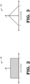
- FIG. 2 is a graph 200 of a probability distribution of a uniformly distributed random number generated by the random number source 126 in accordance with some embodiments.
- the value range of the uniformly distributed random number is normalized to have a value range from -1 to 1. Because the random number is uniformly distributed, the probability P of the random number having any value within the range of -1 to 1 is the same, giving the probability distribution a flat shape or spectrum.
- the delta-sigma modulator 104 is implemented as a multi-stage noise shaping (MASH 1-1-1) structure with a noise shaping characteristic of +60 dB/decade and the loop filter 114 is implemented as at least a third order filter. In other embodiments, other implementations of the delta-sigma modulator 104 are used, and characteristics of the loop filter 114 are selected to reject delta-sigma quantization noise from the output.
- MASH 1-1-1-1 multi-stage noise shaping
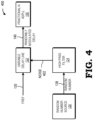
- FIG. 4 is a block diagram 400 of the fractional-N ADPLL 150 having the reference frequency 130 dithered by the variable delay line 122 in accordance with some embodiments.
- the random number 138 generated by the random number source 126 is filtered by the high pass filter 124 to produce noise 402 having a triangular distribution.
- the noise 402 is added to the reference frequency 130 at the variable delay line 122 to produce the randomly modulated delay 140 that is input to the fractional-N ADPLL 150.
- the resulting randomly modulated delay 140 produces a triangularly distributed and noise shaped non-subtractive reference dither that reduces fractional-N spurs in the fractional-N ADPLL 150 without adversely affecting the overall phase noise.
- the randomly modulated delay 140 in conjunction with the higher order loop filter 114 cancels the delta-sigma quantization noise without requiring active control or calibration.
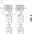
- FIG. 7 is a block diagram of a system 700 including the fractional-N ADPLL 150 having a frequency reference dithered by the variable delay line 122 with digital control and a dynamic element matching module 702 in accordance with some embodiments.
- thermal noise serves as a uniform random source and the triangularly distributed random signal, such as noise 402 in FIG. 4 , is generated by high-pass filtering the output from the uniform random source.
- the system 700 includes a linear-feedback shift register (LFSR) 704 as a uniform pseudo-random source and a simple finite impulse response high-pass filter 706 with a z-domain transfer function 1 - z -1 to generate the triangularly distributed random signal.
- the LFSR 704 produces a statistically even predictable stream of bits having approximately the same number of zeros as ones on average.
- the system 700 includes the dynamic element matching module 702 to increase linearity when using a digitally controlled variable delay line 122.
- the dynamic element matching module 702 includes one or more dynamic element matching circuits. Mismatches among nominally identical circuit elements cause non-linear distortion that appears as spurs caused by the delay line.
- the system 700 monitors the timing relationship between the control signal and the reference propagating through the variable delay line 122. The system 700 ensures that the control signals do not change while a reference clock edge propagates through the variable delay line 122. In some embodiments, the system 700 clocks the control signal generation circuitry with the output of the variable delay line 122.
- the fine resolution variable delay line 808 introduces a variable delay on the order of 100 femtoseconds, while the coarse resolution variable delay line 818 introduces a variable delay on the order of 10 picoseconds.
- a single variable delay line such as that illustrated in FIG. 1 includes on the order of 1000 stages in some embodiments
- a divided variable delay line such as that illustrated in FIG. 8 includes on the order of 20 stages for each of the coarse resolution variable delay line 818 and the fine resolution variable delay line 808 in some embodiments while achieving similar suppression of tones in the quantization noise.
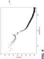
- FIG. 9 is a graph 900 illustrating noise in a fractional-N ADPLL without dithering by a delay line.
- the graph 900 depicts the output noise spectrum of an example fractional-N ADPLL with a ratio of output to input frequency of 66.0001 without dither enabled.
- the spectrum contains large spurs, for example, at 10 kilohertz, which limit the usage of the fractional-N ADPLL.
- FIG. 10 is a graph 1000 illustrating noise reduction in a fractional-N ADPLL having a frequency reference dithered by a delay line in accordance with some embodiments.
- the graph 900 depicts the output noise spectrum of an example fractional-N ADPLL with a ratio of output to input frequency of 66.0001 with dither enabled. The spectrum is free of any visible spurs.
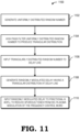
- FIG. 11 is a flow diagram of a method 1100 of dithering a phase of a reference clock signal at an input of a fractional-n ADPLL with a dithering signal having a triangular distribution in accordance with some embodiments.
- the method 1100 is described with respect to an example implementation of the system 100 of FIG. 1 .
- the system 100 includes the fractional-N ADPLL 150 in which the frequency control word is modulated by the delta-sigma modulator 104, which introduces spurious tones due to regular quantization patterns in the feedback path.
- the random number source 126 generates a uniformly distributed random number 138 having a flat spectrum.
- the random number source 126 is implemented as the LFSR 704.
- the high pass filter 124 high-pass filters the uniformly distributed random number 138 to produce a random number having a triangular distribution to use as the delay control 142 input to the variable delay line 122.
- the high pass filter 124 is a first order high pass filter that differentiates the uniformly distributed random number 138 such that the probability distribution of the differences between the normalized values of the uniformly distributed random number follows a triangular distribution.
- the triangularly distributed random number is input to the variable delay line 122.
- variable delay line 122 generates a randomly modulated delay 140 having a triangular distribution.
- the variable delay line 122 is controlled by a digital signal and is implemented in either the analog domain or the digital domain.
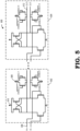
- the variable delay line 122 includes a plurality of unit delay cells 502, 504 and varies either the delay of each unit delay cell 502, 504 or the number of unit delay cells 502, 504 that the signal that is to be delayed traverses.
- a dynamic element matching module 702 is included to randomize mismatch to eliminate spurs from the variable delay line 122.
- the variable delay line 122 is implemented as a single delay line, while in other embodiments the variable delay line 122 is split into a coarse resolution variable delay line 818 and a fine resolution variable delay line 808.
- the randomly modulated delay 140 is input to the fractional-N ADPLL 150 to reduce spurious tones resulting from delta-sigma modulation of the frequency control word 132.
- additional control signals can be added to control the amount of dither to support dithering for multiple TDC resolutions.
- certain aspects of the techniques described above may implemented by one or more processors of a processing system executing software.
- the software comprises one or more sets of executable instructions stored or otherwise tangibly embodied on a non-transitory computer readable storage medium.
- the software can include the instructions and certain data that, when executed by the one or more processors, manipulate the one or more processors to perform one or more aspects of the techniques described above.
- the non-transitory computer readable storage medium can include, for example, a magnetic or optical disk storage device, solid state storage devices such as Flash memory, a cache, random access memory (RAM) or other non-volatile memory device or devices, and the like.
- the executable instructions stored on the non-transitory computer readable storage medium may be in source code, assembly language code, object code, or other instruction format that is interpreted or otherwise executable by one or more processors.
- a computer readable storage medium may include any storage medium, or combination of storage media, accessible by a computer system during use to provide instructions and/or data to the computer system.
- Such storage media can include, but is not limited to, optical media (e.g., compact disc (CD), digital versatile disc (DVD), Blu-Ray disc), magnetic media (e.g., floppy disc, magnetic tape, or magnetic hard drive), volatile memory (e.g., random access memory (RAM) or cache), non-volatile memory (e.g., read-only memory (ROM) or Flash memory), or microelectromechanical systems (MEMS)-based storage media.
- optical media e.g., compact disc (CD), digital versatile disc (DVD), Blu-Ray disc
- magnetic media e.g., floppy disc, magnetic tape, or magnetic hard drive
- volatile memory e.g., random access memory (RAM) or cache
- non-volatile memory e.g., read-only memory (ROM) or Flash memory
- MEMS microelectro
- the computer readable storage medium may be embedded in the computing system (e.g., system RAM or ROM), fixedly attached to the computing system (e.g., a magnetic hard drive), removably attached to the computing system (e.g., an optical disc or Universal Serial Bus (USB)-based Flash memory), or coupled to the computer system via a wired or wireless network (e.g., network accessible storage (NAS)).
- system RAM or ROM system RAM or ROM
- USB Universal Serial Bus
- NAS network accessible storage
Landscapes
- Compression, Expansion, Code Conversion, And Decoders (AREA)
Claims (8)
- Verfahren, umfassend:
Anwenden von Dithering an einem Eingangsfrequenzsteuerwort (FCW.I) eines ganzzahligen, volldigitalen Phasenregelkreises, ADPLL, sodass der ADPLL als ein Fraktional-n-ADPLL (150) fungiert, wobei der ADPLL umfasst:einen Delta-Sigma-Modulator (104), der ausgelegt ist zum Anwenden von Dithering am Eingangsfrequenzsteuerwort (FCW.I) mit einem fraktionalen Frequenzsteuerwortsignal (FCW.F),einen Referenzphasengenerator (110), der ausgelegt ist zum Integrieren des Eingangsfrequenzsteuerworts, an dem Dithering angewendet wurde, um eine Referenzphase (PHI_REF) zu erzeugen,einen Phasendetektor (112), der ausgelegt ist zum Vergleichen der Referenzphase (PHI_REF) mit einer Rückkopplungsphase (PHV),ein Schleifenfilter (114), das ausgelegt ist zum Empfangen des Phasenvergleichsergebnisses (PHE) vom Phasendetektor (112) und Erzeugen von Steuersignalen (PVT, ACQ, TR),einen digital gesteuerten Oszillator, DCO, (116), der ausgelegt ist zum Empfangen von Steuersignalen (PVT, ACQ, TR), und Erzeugen eines Ausgangssignals (CLK_OUT),einen Rückkopplungspfad einschließlich eines Zählers (118) und eines Zeit-Digital-Wandlers, TDC, (120), der ausgelegt ist zum Empfangen einer verzögerungsmodulierten Frequenzreferenz (140) und des Ausgangssignals (CLK_OUT) und Erzeugen der Rückkopplungsphase (PHV), undeine Verzögerungsleitung (122), die ausgelegt ist zum Empfangen einer Frequenzreferenz (FREF) und Erzeugen der verzögerungsmodulierten Frequenzreferenz (140); undErzeugen einer zufällig modulierten Verzögerung basierend auf einer einheitlich verteilten Zufallszahl mit einem flachen Spektrum, das durch ein Hochpassfilter (124) geformt wird, wobei die Zufallszahl die Dreiecksverteilung aufweist, die nach der Formung durch das Hochpassfilter mindestens q bis -q überspannt;Hinzufügen der zufällig modulierten Verzögerung, die eine Dreiecksverteilung aufweist, zu der Frequenzreferenz an einem Eingang des Fraktional-n-ADPLL, durch Modulieren der Verzögerung der Verzögerungsleitung (122), um die verzögerungsmodulierte Frequenzreferenz (140) zu erzeugen, die dem Eingang des Fraktional-n-ADPLL bereitgestellt wird, wobei ein Bereich der zufällig modulierten Verzögerung mindestens q bis -q überspannt, wobei q ein Quantisierungsschritt des Zeit-Digital-Wandlers (120) des ADPLL ist. - Verfahren nach Anspruch 1, wobei das Hinzufügen der zufällig modulierten Verzögerung umfasst:Empfangen der Frequenzreferenz (130) durch die Verzögerungsleitung (122), wobei die Verzögerungsleitung eine Vielzahl von Verzögerungszellen umfasst; undVariieren mindestens eines von Folgendem:eine Verzögerung jeder Verzögerungszelle; undeine Anzahl von Verzögerungszellen, die die Frequenzreferenz durchläuft.
- Verfahren nach Anspruch 2, wobei die Verzögerungsleitung eine Feinverzögerungsleitung und eine Grobverzögerungsleitung umfasst.
- Verfahren nach Anspruch 3, ferner umfassend:
Steuern der Feinverzögerungsleitung unabhängig vom Steuern der Grobverzögerungsleitung. - Volldigitaler Phasenregelkreis, ADPLL, umfassend:einen Delta-Sigma-Modulator (104), der ausgelegt ist zum Anwenden von Dithering an einem Eingangsfrequenzsteuerwort (FCW.I) mit einem fraktionalen Frequenzsteuerwortsignal (FCW.F),einen Referenzphasengenerator (110), der ausgelegt ist zum Integrieren des Eingangsfrequenzsteuerworts, an dem Dithering angewendet wurde, um eine Referenzphase (PHI_REF) zu erzeugen,einen Phasendetektor (112), der ausgelegt ist zum Vergleichen der Referenzphase (PHI_REF) mit einer Rückkopplungsphase (PHV),ein Schleifenfilter (114), das ausgelegt ist zum Empfangen des Phasenvergleichsergebnisses (PHE) vom Phasendetektor (112) und Erzeugen von Steuersignalen (PVT, ACQ, TR),einen digital gesteuerten Oszillator, DCO, (116), der ausgelegt ist zum Empfangen von Steuersignalen (PVT, ACQ, TR), und Erzeugen eines Ausgangssignals (CLK_OUT),einen Rückkopplungspfad einschließlich eines Zählers (118) und eines Zeit-Digital-Wandlers, TDC, (120), der ausgelegt ist zum Empfangen einer verzögerungsmodulierten Frequenzreferenz (140) und des Ausgangssignals (CLK_OUT) und Erzeugen der Rückkopplungsphase (PHV), und eine Verzögerungsleitung (122), die ausgelegt ist zum Empfangen einer Frequenzreferenz (FREF) und Erzeugen der verzögerungsmodulierten Frequenzreferenz (140); wobeidie Verzögerungsleitung ferner ausgelegt ist zum Hinzufügen einer zufällig modulierten Verzögerung zu einer Frequenzreferenz (FREF) des ADPLL durch Modulieren der Verzögerung der Verzögerungsleitung (122), um die verzögerungsmodulierte Frequenzreferenz (140) zu erzeugen,wobei die zufällig modulierte Verzögerung eine Dreiecksverteilung zu der Frequenzreferenz an einem Eingang des ADPLL aufweist;wobei ein Bereich der zufällig modulierten Verzögerung mindestens q bis -q überspannt, wobei q ein Quantisierungsschritt des Zeit-Digital-Wandlers ist;wobei ein Hochpassfilter (124) ausgelegt ist zum Formen einheitlich verteilter Zufallszahlen mit einem flachen Spektrum in die Dreiecksverteilung, um die zufällig modulierte Verzögerung zu erzeugen; undwobei die Dreiecksverteilung nach dem Formen durch das Hochpassfilter mindestens q bis -q überspannt.
- ADPLL nach Anspruch 5, wobei die Verzögerungsleitung eine Vielzahl von Verzögerungszellen umfasst und ausgelegt ist zum Empfangen der Frequenzreferenz (130) und Variieren mindestens eines von Folgendem:eine Verzögerung jeder Verzögerungszelle; undeine Anzahl von Verzögerungszellen, die die Frequenzreferenz durchläuft.
- ADPLL nach Anspruch 6, wobei die Verzögerungsleitung eine Feinverzögerungsleitung und eine Grobverzögerungsleitung umfasst.
- ADPLL nach Anspruch 7, wobei die Feinverzögerungsleitung unabhängig von der Grobverzögerungsleitung gesteuert wird.
Applications Claiming Priority (1)
| Application Number | Priority Date | Filing Date | Title |
|---|---|---|---|
| US17/708,681 US11658666B1 (en) | 2022-03-30 | 2022-03-30 | Fractional-N ADPLL with reference dithering |
Publications (2)
| Publication Number | Publication Date |
|---|---|
| EP4258552A1 EP4258552A1 (de) | 2023-10-11 |
| EP4258552B1 true EP4258552B1 (de) | 2025-04-09 |
Family
ID=85382554
Family Applications (1)
| Application Number | Title | Priority Date | Filing Date |
|---|---|---|---|
| EP23158493.9A Active EP4258552B1 (de) | 2022-03-30 | 2023-02-24 | Fraktional-n-adpll mit referenzdithering |
Country Status (2)
| Country | Link |
|---|---|
| US (1) | US11658666B1 (de) |
| EP (1) | EP4258552B1 (de) |
Families Citing this family (2)
| Publication number | Priority date | Publication date | Assignee | Title |
|---|---|---|---|---|
| US12308860B2 (en) * | 2021-12-21 | 2025-05-20 | University College Dublin | Apparatus for mitigating nonlinearity-induced spurs and noise in a fractional-N frequency synthesizer |
| US20230327681A1 (en) * | 2022-04-11 | 2023-10-12 | University College Dublin | Digital delta sigma modulator with inherent spur immunity after nonlinear distortion |
Family Cites Families (10)
| Publication number | Priority date | Publication date | Assignee | Title |
|---|---|---|---|---|
| US20050186920A1 (en) | 2004-02-19 | 2005-08-25 | Texas Instruments Incorporated | Apparatus for and method of noise suppression and dithering to improve resolution quality in a digital RF processor |
| US7570182B2 (en) | 2006-09-15 | 2009-08-04 | Texas Instruments Incorporated | Adaptive spectral noise shaping to improve time to digital converter quantization resolution using dithering |
| US20120244824A1 (en) | 2007-02-12 | 2012-09-27 | Texas Instruments Incorporated | Minimization of rms phase error in a phase locked loop by dithering of a frequency reference |
| US8830001B2 (en) * | 2007-06-22 | 2014-09-09 | Texas Instruments Incorporated | Low power all digital PLL architecture |
| US8134411B2 (en) | 2008-04-17 | 2012-03-13 | Texas Instruments Incorporated | Computation spreading utilizing dithering for spur reduction in a digital phase lock loop |
| EP2194646B1 (de) * | 2008-12-04 | 2013-01-02 | STMicroelectronics Srl | Verfahren zur Verbesserung der Rauschcharakteristiken von einem volldigitalen Phasenregelkreis (ADPLL) und einem relativen ADPLL |
| US8395428B2 (en) * | 2010-09-30 | 2013-03-12 | St-Ericsson Sa | Reference clock sampling digital PLL |
| CN107528588A (zh) * | 2016-06-21 | 2017-12-29 | 马维尔国际贸易有限公司 | 模拟分数n锁相环 |
| US10122378B2 (en) * | 2017-03-16 | 2018-11-06 | Samsung Electronics Co., Ltd. | Digital-to-time converter and operating method thereof |
| US11271584B2 (en) * | 2020-07-08 | 2022-03-08 | Korean Advanced Institute Of Science And Technology | Integrated circuit, electronic device including the same, and operating method thereof |
-
2022
- 2022-03-30 US US17/708,681 patent/US11658666B1/en active Active
-
2023
- 2023-02-24 EP EP23158493.9A patent/EP4258552B1/de active Active
Also Published As
| Publication number | Publication date |
|---|---|
| EP4258552A1 (de) | 2023-10-11 |
| US11658666B1 (en) | 2023-05-23 |
Similar Documents
| Publication | Publication Date | Title |
|---|---|---|
| Hwang et al. | A low-jitter and low-fractional-spur ring-DCO-based fractional-N digital PLL using a DTC’s second-/third-order nonlinearity cancellation and a probability-density-shaping ΔΣM | |
| US11817868B2 (en) | Apparatus for digital frequency synthesizer with sigma-delta modulator and associated methods | |
| Park et al. | 32.1 A 365fsrms-jitter and-63dBc-fractional spur 5.3 GHz-ring-DCO-based fractional-N DPLL using a DTC second/third-order nonlinearity cancelation and a probability-density-shaping ΔΣM | |
| US10090845B1 (en) | Fraction-N digital PLL capable of canceling quantization noise from sigma-delta modulator | |
| US10979059B1 (en) | Successive approximation register analog to digital converter based phase-locked loop with programmable range | |
| US9319051B2 (en) | Digital PLL with hybrid phase/frequency detector and digital noise cancellation | |
| US10763869B2 (en) | Apparatus for digital frequency synthesizers and associated methods | |
| US8433024B2 (en) | Spread spectrum clock generator and method for adjusting spread amount | |
| US9246499B2 (en) | Digital phase lock loop circuit including finite impulse response filtering to reduce aliasing of quantization noise | |
| EP4258552B1 (de) | Fraktional-n-adpll mit referenzdithering | |
| US8198929B2 (en) | Dynamic element matching for time-to-digital converters | |
| US7605665B2 (en) | Fractional-N phase locked loop | |
| US20100289541A1 (en) | Digital phase-locked loop circuit including a phase delay quantizer and method of use | |
| US20220014205A1 (en) | System and method for low jitter phase-lock loop based frequency synthesizer | |
| EP1538752A1 (de) | Taktimpulserzeugungsgerät mit reduziertem Phasenzittern | |
| CN101841326A (zh) | 混合模式锁相环及减少全数字锁相环中分数杂散的方法 | |
| Levantino et al. | Nonlinearity cancellation in digital PLLs | |
| Elmallah et al. | A 3.2-GHz 405 fs rms jitter–237.2 dB FoM JIT ring-based fractional-N synthesizer | |
| Xu et al. | A spread-spectrum clock generator with FIR-embedded binary phase detection and 1-bit high-order ΔΣ modulation | |
| US20250167797A1 (en) | Dtc linearization via mismatch-noise cancellation for digital fractional-n plls | |
| Wang et al. | Comparison of DTC-related spurs in fractional-N digital PLLs with MASH-and-ENOP-based divider controllers | |
| EP3523878B1 (de) | Digital steuerbarer oszillator mit hoher genauigkeit | |
| US9019017B2 (en) | Digitally controlled oscillator and digital PLL including the same | |
| Temporiti et al. | Insights into wideband fractional all-digital PLLs for RF applications | |
| Pamarti | Digital techniques for integrated frequency synthesizers: A tutorial |
Legal Events
| Date | Code | Title | Description |
|---|---|---|---|
| PUAI | Public reference made under article 153(3) epc to a published international application that has entered the european phase |
Free format text: ORIGINAL CODE: 0009012 |
|
| STAA | Information on the status of an ep patent application or granted ep patent |
Free format text: STATUS: THE APPLICATION HAS BEEN PUBLISHED |
|
| AK | Designated contracting states |
Kind code of ref document: A1 Designated state(s): AL AT BE BG CH CY CZ DE DK EE ES FI FR GB GR HR HU IE IS IT LI LT LU LV MC ME MK MT NL NO PL PT RO RS SE SI SK SM TR |
|
| STAA | Information on the status of an ep patent application or granted ep patent |
Free format text: STATUS: REQUEST FOR EXAMINATION WAS MADE |
|
| 17P | Request for examination filed |
Effective date: 20240411 |
|
| RBV | Designated contracting states (corrected) |
Designated state(s): AL AT BE BG CH CY CZ DE DK EE ES FI FR GB GR HR HU IE IS IT LI LT LU LV MC ME MK MT NL NO PL PT RO RS SE SI SK SM TR |
|
| GRAP | Despatch of communication of intention to grant a patent |
Free format text: ORIGINAL CODE: EPIDOSNIGR1 |
|
| STAA | Information on the status of an ep patent application or granted ep patent |
Free format text: STATUS: GRANT OF PATENT IS INTENDED |
|
| INTG | Intention to grant announced |
Effective date: 20241205 |
|
| GRAS | Grant fee paid |
Free format text: ORIGINAL CODE: EPIDOSNIGR3 |
|
| GRAA | (expected) grant |
Free format text: ORIGINAL CODE: 0009210 |
|
| STAA | Information on the status of an ep patent application or granted ep patent |
Free format text: STATUS: THE PATENT HAS BEEN GRANTED |
|
| AK | Designated contracting states |
Kind code of ref document: B1 Designated state(s): AL AT BE BG CH CY CZ DE DK EE ES FI FR GB GR HR HU IE IS IT LI LT LU LV MC ME MK MT NL NO PL PT RO RS SE SI SK SM TR |
|
| REG | Reference to a national code |
Ref country code: GB Ref legal event code: FG4D |
|
| REG | Reference to a national code |
Ref country code: CH Ref legal event code: EP |
|
| REG | Reference to a national code |
Ref country code: DE Ref legal event code: R096 Ref document number: 602023002776 Country of ref document: DE |
|
| REG | Reference to a national code |
Ref country code: IE Ref legal event code: FG4D |
|
| REG | Reference to a national code |
Ref country code: NL Ref legal event code: MP Effective date: 20250409 |
|
| PG25 | Lapsed in a contracting state [announced via postgrant information from national office to epo] |
Ref country code: NL Free format text: LAPSE BECAUSE OF FAILURE TO SUBMIT A TRANSLATION OF THE DESCRIPTION OR TO PAY THE FEE WITHIN THE PRESCRIBED TIME-LIMIT Effective date: 20250409 |
|
| REG | Reference to a national code |
Ref country code: AT Ref legal event code: MK05 Ref document number: 1784479 Country of ref document: AT Kind code of ref document: T Effective date: 20250409 |
|
| PG25 | Lapsed in a contracting state [announced via postgrant information from national office to epo] |
Ref country code: PT Free format text: LAPSE BECAUSE OF FAILURE TO SUBMIT A TRANSLATION OF THE DESCRIPTION OR TO PAY THE FEE WITHIN THE PRESCRIBED TIME-LIMIT Effective date: 20250811 Ref country code: FI Free format text: LAPSE BECAUSE OF FAILURE TO SUBMIT A TRANSLATION OF THE DESCRIPTION OR TO PAY THE FEE WITHIN THE PRESCRIBED TIME-LIMIT Effective date: 20250409 Ref country code: ES Free format text: LAPSE BECAUSE OF FAILURE TO SUBMIT A TRANSLATION OF THE DESCRIPTION OR TO PAY THE FEE WITHIN THE PRESCRIBED TIME-LIMIT Effective date: 20250409 |
|
| REG | Reference to a national code |
Ref country code: LT Ref legal event code: MG9D |
|
| PG25 | Lapsed in a contracting state [announced via postgrant information from national office to epo] |
Ref country code: GR Free format text: LAPSE BECAUSE OF FAILURE TO SUBMIT A TRANSLATION OF THE DESCRIPTION OR TO PAY THE FEE WITHIN THE PRESCRIBED TIME-LIMIT Effective date: 20250710 Ref country code: NO Free format text: LAPSE BECAUSE OF FAILURE TO SUBMIT A TRANSLATION OF THE DESCRIPTION OR TO PAY THE FEE WITHIN THE PRESCRIBED TIME-LIMIT Effective date: 20250709 |
|
| PG25 | Lapsed in a contracting state [announced via postgrant information from national office to epo] |
Ref country code: PL Free format text: LAPSE BECAUSE OF FAILURE TO SUBMIT A TRANSLATION OF THE DESCRIPTION OR TO PAY THE FEE WITHIN THE PRESCRIBED TIME-LIMIT Effective date: 20250409 |
|
| PG25 | Lapsed in a contracting state [announced via postgrant information from national office to epo] |
Ref country code: BG Free format text: LAPSE BECAUSE OF FAILURE TO SUBMIT A TRANSLATION OF THE DESCRIPTION OR TO PAY THE FEE WITHIN THE PRESCRIBED TIME-LIMIT Effective date: 20250409 |
|
| PG25 | Lapsed in a contracting state [announced via postgrant information from national office to epo] |
Ref country code: HR Free format text: LAPSE BECAUSE OF FAILURE TO SUBMIT A TRANSLATION OF THE DESCRIPTION OR TO PAY THE FEE WITHIN THE PRESCRIBED TIME-LIMIT Effective date: 20250409 |
|
| PG25 | Lapsed in a contracting state [announced via postgrant information from national office to epo] |
Ref country code: AT Free format text: LAPSE BECAUSE OF FAILURE TO SUBMIT A TRANSLATION OF THE DESCRIPTION OR TO PAY THE FEE WITHIN THE PRESCRIBED TIME-LIMIT Effective date: 20250409 |
|
| PG25 | Lapsed in a contracting state [announced via postgrant information from national office to epo] |
Ref country code: RS Free format text: LAPSE BECAUSE OF FAILURE TO SUBMIT A TRANSLATION OF THE DESCRIPTION OR TO PAY THE FEE WITHIN THE PRESCRIBED TIME-LIMIT Effective date: 20250709 |
|
| PG25 | Lapsed in a contracting state [announced via postgrant information from national office to epo] |
Ref country code: IS Free format text: LAPSE BECAUSE OF FAILURE TO SUBMIT A TRANSLATION OF THE DESCRIPTION OR TO PAY THE FEE WITHIN THE PRESCRIBED TIME-LIMIT Effective date: 20250809 |
|
| PG25 | Lapsed in a contracting state [announced via postgrant information from national office to epo] |
Ref country code: LV Free format text: LAPSE BECAUSE OF FAILURE TO SUBMIT A TRANSLATION OF THE DESCRIPTION OR TO PAY THE FEE WITHIN THE PRESCRIBED TIME-LIMIT Effective date: 20250409 |
|
| REG | Reference to a national code |
Ref country code: DE Ref legal event code: R097 Ref document number: 602023002776 Country of ref document: DE |
|
| PG25 | Lapsed in a contracting state [announced via postgrant information from national office to epo] |
Ref country code: DK Free format text: LAPSE BECAUSE OF FAILURE TO SUBMIT A TRANSLATION OF THE DESCRIPTION OR TO PAY THE FEE WITHIN THE PRESCRIBED TIME-LIMIT Effective date: 20250409 Ref country code: SM Free format text: LAPSE BECAUSE OF FAILURE TO SUBMIT A TRANSLATION OF THE DESCRIPTION OR TO PAY THE FEE WITHIN THE PRESCRIBED TIME-LIMIT Effective date: 20250409 |
|
| PG25 | Lapsed in a contracting state [announced via postgrant information from national office to epo] |
Ref country code: CZ Free format text: LAPSE BECAUSE OF FAILURE TO SUBMIT A TRANSLATION OF THE DESCRIPTION OR TO PAY THE FEE WITHIN THE PRESCRIBED TIME-LIMIT Effective date: 20250409 |
|
| PG25 | Lapsed in a contracting state [announced via postgrant information from national office to epo] |
Ref country code: EE Free format text: LAPSE BECAUSE OF FAILURE TO SUBMIT A TRANSLATION OF THE DESCRIPTION OR TO PAY THE FEE WITHIN THE PRESCRIBED TIME-LIMIT Effective date: 20250409 |
|
| PG25 | Lapsed in a contracting state [announced via postgrant information from national office to epo] |
Ref country code: SK Free format text: LAPSE BECAUSE OF FAILURE TO SUBMIT A TRANSLATION OF THE DESCRIPTION OR TO PAY THE FEE WITHIN THE PRESCRIBED TIME-LIMIT Effective date: 20250409 |
|
| PG25 | Lapsed in a contracting state [announced via postgrant information from national office to epo] |
Ref country code: IT Free format text: LAPSE BECAUSE OF FAILURE TO SUBMIT A TRANSLATION OF THE DESCRIPTION OR TO PAY THE FEE WITHIN THE PRESCRIBED TIME-LIMIT Effective date: 20250409 |
|
| PLBE | No opposition filed within time limit |
Free format text: ORIGINAL CODE: 0009261 |
|
| STAA | Information on the status of an ep patent application or granted ep patent |
Free format text: STATUS: NO OPPOSITION FILED WITHIN TIME LIMIT |
|
| REG | Reference to a national code |
Ref country code: CH Ref legal event code: L10 Free format text: ST27 STATUS EVENT CODE: U-0-0-L10-L00 (AS PROVIDED BY THE NATIONAL OFFICE) Effective date: 20260218 |
|
| 26N | No opposition filed |
Effective date: 20260112 |
|
| PGFP | Annual fee paid to national office [announced via postgrant information from national office to epo] |
Ref country code: DE Payment date: 20260121 Year of fee payment: 4 |
|
| PGFP | Annual fee paid to national office [announced via postgrant information from national office to epo] |
Ref country code: FR Payment date: 20260121 Year of fee payment: 4 |