EP4258337A1 - Insulated board and power converter - Google Patents
Insulated board and power converter Download PDFInfo
- Publication number
- EP4258337A1 EP4258337A1 EP21900266.4A EP21900266A EP4258337A1 EP 4258337 A1 EP4258337 A1 EP 4258337A1 EP 21900266 A EP21900266 A EP 21900266A EP 4258337 A1 EP4258337 A1 EP 4258337A1
- Authority
- EP
- European Patent Office
- Prior art keywords
- conductor
- conductors
- insulating plate
- insulating
- insulating substrate
- Prior art date
- Legal status (The legal status is an assumption and is not a legal conclusion. Google has not performed a legal analysis and makes no representation as to the accuracy of the status listed.)
- Granted
Links
Images





Classifications
-
- H—ELECTRICITY
- H10—SEMICONDUCTOR DEVICES; ELECTRIC SOLID-STATE DEVICES NOT OTHERWISE PROVIDED FOR
- H10W—GENERIC PACKAGES, INTERCONNECTIONS, CONNECTORS OR OTHER CONSTRUCTIONAL DETAILS OF DEVICES COVERED BY CLASS H10
- H10W40/00—Arrangements for thermal protection or thermal control
- H10W40/20—Arrangements for cooling
- H10W40/25—Arrangements for cooling characterised by their materials
- H10W40/255—Arrangements for cooling characterised by their materials having a laminate or multilayered structure, e.g. direct bond copper [DBC] ceramic substrates
-
- H—ELECTRICITY
- H10—SEMICONDUCTOR DEVICES; ELECTRIC SOLID-STATE DEVICES NOT OTHERWISE PROVIDED FOR
- H10W—GENERIC PACKAGES, INTERCONNECTIONS, CONNECTORS OR OTHER CONSTRUCTIONAL DETAILS OF DEVICES COVERED BY CLASS H10
- H10W40/00—Arrangements for thermal protection or thermal control
- H10W40/20—Arrangements for cooling
- H10W40/22—Arrangements for cooling characterised by their shape, e.g. having conical or cylindrical projections
- H10W40/226—Arrangements for cooling characterised by their shape, e.g. having conical or cylindrical projections characterised by projecting parts, e.g. fins to increase surface area
- H10W40/228—Arrangements for cooling characterised by their shape, e.g. having conical or cylindrical projections characterised by projecting parts, e.g. fins to increase surface area the projecting parts being wire-shaped or pin-shaped
-
- H—ELECTRICITY
- H10—SEMICONDUCTOR DEVICES; ELECTRIC SOLID-STATE DEVICES NOT OTHERWISE PROVIDED FOR
- H10W—GENERIC PACKAGES, INTERCONNECTIONS, CONNECTORS OR OTHER CONSTRUCTIONAL DETAILS OF DEVICES COVERED BY CLASS H10
- H10W44/00—Electrical arrangements for controlling or matching impedance
- H10W44/501—Inductive arrangements
-
- H—ELECTRICITY
- H10—SEMICONDUCTOR DEVICES; ELECTRIC SOLID-STATE DEVICES NOT OTHERWISE PROVIDED FOR
- H10W—GENERIC PACKAGES, INTERCONNECTIONS, CONNECTORS OR OTHER CONSTRUCTIONAL DETAILS OF DEVICES COVERED BY CLASS H10
- H10W90/00—Package configurations
-
- H—ELECTRICITY
- H02—GENERATION; CONVERSION OR DISTRIBUTION OF ELECTRIC POWER
- H02M—APPARATUS FOR CONVERSION BETWEEN AC AND AC, BETWEEN AC AND DC, OR BETWEEN DC AND DC, AND FOR USE WITH MAINS OR SIMILAR POWER SUPPLY SYSTEMS; CONVERSION OF DC OR AC INPUT POWER INTO SURGE OUTPUT POWER; CONTROL OR REGULATION THEREOF
- H02M1/00—Details of apparatus for conversion
- H02M1/32—Means for protecting converters other than automatic disconnection
- H02M1/327—Means for protecting converters other than automatic disconnection against abnormal temperatures
-
- H—ELECTRICITY
- H02—GENERATION; CONVERSION OR DISTRIBUTION OF ELECTRIC POWER
- H02M—APPARATUS FOR CONVERSION BETWEEN AC AND AC, BETWEEN AC AND DC, OR BETWEEN DC AND DC, AND FOR USE WITH MAINS OR SIMILAR POWER SUPPLY SYSTEMS; CONVERSION OF DC OR AC INPUT POWER INTO SURGE OUTPUT POWER; CONTROL OR REGULATION THEREOF
- H02M7/00—Conversion of AC power input into DC power output; Conversion of DC power input into AC power output
- H02M7/003—Constructional details, e.g. physical layout, assembly, wiring or busbar connections
-
- H—ELECTRICITY
- H10—SEMICONDUCTOR DEVICES; ELECTRIC SOLID-STATE DEVICES NOT OTHERWISE PROVIDED FOR
- H10W—GENERIC PACKAGES, INTERCONNECTIONS, CONNECTORS OR OTHER CONSTRUCTIONAL DETAILS OF DEVICES COVERED BY CLASS H10
- H10W70/00—Package substrates; Interposers; Redistribution layers [RDL]
- H10W70/60—Insulating or insulated package substrates; Interposers; Redistribution layers
- H10W70/611—Insulating or insulated package substrates; Interposers; Redistribution layers for connecting multiple chips together
-
- H—ELECTRICITY
- H10—SEMICONDUCTOR DEVICES; ELECTRIC SOLID-STATE DEVICES NOT OTHERWISE PROVIDED FOR
- H10W—GENERIC PACKAGES, INTERCONNECTIONS, CONNECTORS OR OTHER CONSTRUCTIONAL DETAILS OF DEVICES COVERED BY CLASS H10
- H10W70/00—Package substrates; Interposers; Redistribution layers [RDL]
- H10W70/60—Insulating or insulated package substrates; Interposers; Redistribution layers
- H10W70/62—Insulating or insulated package substrates; Interposers; Redistribution layers characterised by their interconnections
- H10W70/65—Shapes or dispositions of interconnections
-
- H—ELECTRICITY
- H10—SEMICONDUCTOR DEVICES; ELECTRIC SOLID-STATE DEVICES NOT OTHERWISE PROVIDED FOR
- H10W—GENERIC PACKAGES, INTERCONNECTIONS, CONNECTORS OR OTHER CONSTRUCTIONAL DETAILS OF DEVICES COVERED BY CLASS H10
- H10W72/00—Interconnections or connectors in packages
- H10W72/50—Bond wires
- H10W72/531—Shapes of wire connectors
- H10W72/5363—Shapes of wire connectors the connected ends being wedge-shaped
-
- H—ELECTRICITY
- H10—SEMICONDUCTOR DEVICES; ELECTRIC SOLID-STATE DEVICES NOT OTHERWISE PROVIDED FOR
- H10W—GENERIC PACKAGES, INTERCONNECTIONS, CONNECTORS OR OTHER CONSTRUCTIONAL DETAILS OF DEVICES COVERED BY CLASS H10
- H10W74/00—Encapsulations, e.g. protective coatings
-
- H—ELECTRICITY
- H10—SEMICONDUCTOR DEVICES; ELECTRIC SOLID-STATE DEVICES NOT OTHERWISE PROVIDED FOR
- H10W—GENERIC PACKAGES, INTERCONNECTIONS, CONNECTORS OR OTHER CONSTRUCTIONAL DETAILS OF DEVICES COVERED BY CLASS H10
- H10W74/00—Encapsulations, e.g. protective coatings
- H10W74/10—Encapsulations, e.g. protective coatings characterised by their shape or disposition
- H10W74/111—Encapsulations, e.g. protective coatings characterised by their shape or disposition the semiconductor body being completely enclosed
-
- H—ELECTRICITY
- H10—SEMICONDUCTOR DEVICES; ELECTRIC SOLID-STATE DEVICES NOT OTHERWISE PROVIDED FOR
- H10W—GENERIC PACKAGES, INTERCONNECTIONS, CONNECTORS OR OTHER CONSTRUCTIONAL DETAILS OF DEVICES COVERED BY CLASS H10
- H10W74/00—Encapsulations, e.g. protective coatings
- H10W74/10—Encapsulations, e.g. protective coatings characterised by their shape or disposition
- H10W74/111—Encapsulations, e.g. protective coatings characterised by their shape or disposition the semiconductor body being completely enclosed
- H10W74/114—Encapsulations, e.g. protective coatings characterised by their shape or disposition the semiconductor body being completely enclosed by a substrate and the encapsulations
-
- H—ELECTRICITY
- H10—SEMICONDUCTOR DEVICES; ELECTRIC SOLID-STATE DEVICES NOT OTHERWISE PROVIDED FOR
- H10W—GENERIC PACKAGES, INTERCONNECTIONS, CONNECTORS OR OTHER CONSTRUCTIONAL DETAILS OF DEVICES COVERED BY CLASS H10
- H10W76/00—Containers; Fillings or auxiliary members therefor; Seals
- H10W76/10—Containers or parts thereof
- H10W76/12—Containers or parts thereof characterised by their shape
- H10W76/13—Containers comprising a conductive base serving as an interconnection
- H10W76/138—Containers comprising a conductive base serving as an interconnection having another interconnection being formed by a cover plate parallel to the conductive base, e.g. sandwich type
-
- H—ELECTRICITY
- H10—SEMICONDUCTOR DEVICES; ELECTRIC SOLID-STATE DEVICES NOT OTHERWISE PROVIDED FOR
- H10W—GENERIC PACKAGES, INTERCONNECTIONS, CONNECTORS OR OTHER CONSTRUCTIONAL DETAILS OF DEVICES COVERED BY CLASS H10
- H10W90/00—Package configurations
- H10W90/701—Package configurations characterised by the relative positions of pads or connectors relative to package parts
- H10W90/751—Package configurations characterised by the relative positions of pads or connectors relative to package parts of bond wires
- H10W90/754—Package configurations characterised by the relative positions of pads or connectors relative to package parts of bond wires between a chip and a stacked insulating package substrate, interposer or RDL
Definitions
- the present invention relates to an insulating substrate and a power conversion apparatus, and more particularly to an insulating substrate for mounting a semiconductor chip and a power conversion apparatus using the insulating substrate.
- the power semiconductor chip of SiC, GaN, or the like can be driven at a high frequency, passive components such as inductors or capacitors provided in the power conversion apparatus can be downsized. With these effects, it is possible to reduce an overall size of the power conversion apparatus.
- a parasitic inductance Ls of the power conversion apparatus becomes a problem during high-frequency driving.
- a surge voltage ⁇ V is represented by a product of the parasitic inductance Ls and an amount of current per time unit (di/dt).
- the large parasitic inductance Ls causes the large surge voltage ⁇ V to be applied when the semiconductor chip is turned off, and also becomes a source of noise.
- the surge voltage ⁇ V and the noise greatly affect the off-speed.
- PTL 1 discloses an insulating substrate including an insulating plate, a top surface wiring conductor formed on a top surface of the insulating plate, and a back surface wiring conductor formed on a back surface of the insulating plate.
- a semiconductor chip is disposed on the top surface wiring conductor.
- PTL 1 discloses a technique for reducing a parasitic inductance using a bridge terminal provided on the top surface wiring conductor due to an effect of proximity reverse conduction.
- the inventors of the present application have studied structures according to Study Example 1 shown in FIG. 2 and Study Example 2 shown in FIG. 3 as power conversion apparatus 100 for compound semiconductor substrates.
- the power conversion apparatus 100 uses an insulating substrate 1 including an insulating plate 2a, a plurality of conductors 3a formed on a top surface of the insulating plate 2a, and a heat dissipation conductor 5 formed on a back surface of the insulating plate 2a.
- a plurality of semiconductor chips CHP are disposed on the plurality of conductors 3a, and the plurality of conductors 3a and the plurality of semiconductor chips CHP are electrically connected by bonding wires BW as appropriate.
- the heat dissipation conductor 5 is connected to a heat sink 300 via a base plate 200.
- the power conversion apparatus 100 according to Study Example 2 further includes a conductor 3b and an insulating plate 2b between the insulating plate 2a and the heat dissipation conductor 5, thereby forming a multilayer insulating substrate structure.
- the parasitic inductance Ls can be reduced by mutual inductance as compared with Study Example 1.
- an insulating substrate including: a first insulating plate including a top surface and a back surface; a second insulating plate formed on a back surface side of the first insulating plate and including a top surface and a back surface; a plurality of first conductors formed on the top surface of the first insulating plate; a second conductor formed between the back surface of the first insulating plate and the top surface of the second insulating plate; a heat dissipation conductor formed on the back surface of the second insulating plate and electrically insulated from the second conductor; and a plurality of first connection conductors formed inside the first insulating plate in a manner of electrically connecting some of the plurality of first conductors and the second conductor.
- the plurality of first conductors include a first non-connected conductor that is not electrically connected to the second conductor via the plurality of first connection conductors, a protruding conductor is formed in the first insulating plate in a manner of being embedded in the first insulating plate and protruding from the back surface of the first insulating plate, and the protruding conductor is electrically connected to the first non-connected conductor, and is electrically insulated from the second conductor and the heat dissipation conductor.
- an insulating substrate including: a first insulating plate including a top surface and a back surface; a plurality of first conductors formed on the top surface of the first insulating plate; a plurality of second conductors formed on the back surface of the first insulating plate; and a plurality of first connection conductors formed inside the first insulating plate in a manner of electrically connecting some of the plurality of first conductors and some of the plurality of second conductors.
- the plurality of second conductors include a second non-connected conductor electrically insulated from another second conductor, and a heat dissipation conductor is connected to the second non-connected conductor in a manner of protruding from the other second conductor on a back surface side of the first insulating plate.
- an insulating substrate capable of keeping a parasitic inductance low and improving heat dissipation. Reliability of a power conversion apparatus can be improved using such an insulating substrate.
- An X direction, a Y direction, and a Z direction described in the present application intersect with one another and are orthogonal to one another.
- the Z direction is referred to as a vertical direction, an upper-lower direction, a height direction, or a thickness direction of a certain structure.
- An expression "plan view" used in the present application means viewing a plane formed by the X direction and the Y direction from the Z direction.
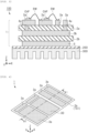
- FIG. 4 is a perspective view showing the insulating substrate 1
- FIG. 5 is a cross-sectional view taken along a line A1-A1 shown in FIG. 4
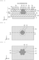
- FIGS. 6 and 7 are plan views showing a layer of the insulating substrate 1, a conductor 3b.
- the insulating substrate 1 includes a multilayer insulating substrate structure in which insulating plates and conductors through which a current flows are stacked for a plurality of layers.
- the insulating substrate 1 includes an insulating plate 2a, an insulating plate 2b, a plurality of conductors 3a, the conductor 3b, a plurality of connection conductors 4a, and a heat dissipation conductor 5.
- the insulating plate 2a includes a top surface TS1 and a back surface BS1. As shown in FIG. 4 , the plurality of conductors 3a are formed on the top surface TS1 of the insulating plate 2a. The plurality of conductors 3a include a non-connected conductor 30.
- the insulating plate 2b is formed on a back surface BS1 side of the insulating plate 2a and has a top surface TS2 and a back surface BS2.
- the conductor 3b is formed between the back surface BS1 of the insulating plate 2a and the top surface TS2 of the insulating plate 2b.
- the plurality of connection conductors 4a are formed in the insulating plate 2a in a manner of electrically connecting some of the plurality of conductors 3a and the conductor 3b.
- the heat dissipation conductor 5 electrically insulated from the conductor 3b is formed on the back surface BS2 of the insulating plate 2b.
- various electronic devices such as a plurality of semiconductor chips, capacitors, and inductors are disposed on the plurality of conductors 3a, and electrical conduction among the electronic devices is formed and a current path is constructed by electrically connecting the plurality of conductors 3a, the plurality of connection conductors 4a, and the conductor 3b.
- a case where one conductor 3b is provided is illustrated here.
- a plurality of conductors 3b may be provided. In this case, a more complicated circuit can be constructed by the plurality of conductors 3b.
- the insulating substrate 1 has a multilayer insulating substrate structure. Therefore, a distance between the plurality of semiconductor chips and the heat dissipation conductor 5 may increase, and heat dissipation may tend to deteriorate.
- the plurality of conductors 3a include the non-connected conductor 30 that is not electrically connected to the conductor 3b via the plurality of connection conductors 4a. Since a heat dissipation path electrically insulated from the current path is provided below the non-connected conductor 30, heat dissipation can be improved.
- a protruding conductor 40 is formed in the insulating plate 2a in a manner of being embedded in the insulating plate 2a and protruding from the back surface BS1 of the insulating plate 2a.
- the protruding conductor 40 is electrically connected to the non-connected conductor 30, and is electrically insulated from the heat dissipation conductor 5 by the insulating plate 2b.
- the protruding conductor 40 is electrically insulated from the conductor 3b by an insulating layer 41 surrounding the protruding conductor 40 in a plan view.
- the parasitic inductance Ls can be kept low, and heat dissipation can be improved.
- a plurality of protruding conductors 40 may be provided as shown in FIG. 7 instead of only one as shown in FIG 6 .
- the plurality of protruding conductors 40 are formed in the insulating plate 2a.
- Each of the plurality of protruding conductors 40 is electrically connected to the non-connected conductor 30, electrically insulated from the conductor 3b by the insulating layer 41, and electrically insulated from the heat dissipation conductor 5 by the insulating plate 2b.
- a planar area of each protruding conductor 40 is smaller than that in FIG. 6 , but heat dissipation can be ensured substantially the same in FIG. 7 as that in FIG. 6 when a total planar area of the plurality of protruding conductors 40 is designed to be substantially the same as that in FIG. 6 .
- the plurality of conductors 3a including the non-connected conductor 30, the conductor 3b, the heat dissipation conductor 5, the plurality of connection conductors 4a, and the protruding conductor 40 are made of, for example, a metal material containing copper (Cu) or aluminum (Al).
- the insulating plate 2a and the insulating plate 2b are made of, for example, a ceramic or resin material.
- FIG. 8 is a perspective view showing the power conversion apparatus 100
- FIGS. 9 and 10 are cross-sectional views taken along a line A2-A2 shown in FIG 8 .
- the line A2-A2 is located on the same straight line as the line A1-A1 shown in FIGS. 4 and 6 .
- the power conversion apparatus 100 includes the insulating substrate 1, a plurality of semiconductor chips CHP, bonding wires BW, a base plate 200 and a heat sink 300.
- the heat sink 300 is connected to the heat dissipation conductor 5 via the base plate 200.
- the heat dissipation conductor 5 and the base plate 200 are connected to each other via a thermal interface material (TIM).
- the base plate 200 and the heat sink 300 are also connected via a TIM.
- the TIM is, for example, a material such as solder or a sintered material.
- Each of the plurality of semiconductor chips CHP has a top surface and a back surface, and back surfaces of the plurality of semiconductor chips CHP are disposed on the plurality of conductors 3a by a TIM. At least one of the plurality of semiconductor chips CHP is provided on the non-connected conductor 30.
- the plurality of semiconductor chips CHP and the plurality of conductors 3a are electrically connected to each other by the bonding wires BW as appropriate.
- capacitors and inductors may be disposed on the plurality of conductors 3a.
- the insulating substrate 1, the plurality of semiconductor chips CHP, and the bonding wires BW may be covered with a protective member 400.
- the protective member 400 is made of an insulating material, and is made of, for example, an insulating gel or a molding resin.
- the semiconductor chip CHP includes, for example, a compound semiconductor substrate of silicon carbide (SiC), gallium nitride (GaN), gallium oxide (Ga 2 O 3 ), or the like, and a transistor such as a MOSFET formed on the compound semiconductor substrate.
- SiC silicon carbide
- GaN gallium nitride
- Ga 2 O 3 gallium oxide
- the bonding wire BW is made of, for example, a metal material containing gold (Au), copper (Cu), or aluminum (Al).
- the plurality of semiconductor chips CHP and the plurality of conductors 3a may be electrically connected by ribbons, bus bars, or the like instead of the bonding wires BW.
- the base plate 200 is made of, for example, a composite material (AlSiC) in which SiC ceramic particles are contained in copper (Cu) or an aluminum alloy, or a composite material (MgSiC) in which SiC ceramic particles are contained in magnesium.
- the heat sink 300 is made of, for example, a metal material containing copper (Cu), iron (Fe), or aluminum.
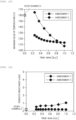
- FIGS. 11 and 12 are graphs showing effects according to Embodiment 1, and are simulation results measured by the inventors of the present application.
- FIGS. 11 and 12 also show effects according to Embodiment 3 described later.
- "Heat area” on a horizontal axis in FIGS. 11 and 12 indicates an area of the protruding conductor 40 in a plan view.
- a temperature rise can be prevented as compared with Study Example 2 ( FIG. 3 ), and the parasitic inductance Ls can be maintained to be substantially the same as that in Study Example 2 ( FIG. 3 ). That is, according to Embodiment 1, it is possible to provide the insulating substrate 1 capable of keeping the parasitic inductance Ls low and improving heat dissipation, and reliability of the power conversion apparatus 100 can be improved using such an insulating substrate 1.
- Embodiment 2 the insulating substrate 1 and the power conversion apparatus 100 according to Embodiment 2 will be described with reference to FIGS. 13 and 14 .
- differences from Embodiment 1 will be mainly described, and the description of points overlapping with Embodiment 1 will be omitted.
- the insulating substrate 1 according to Embodiment 2 has a multilayer insulating substrate structure in which more insulating plates and conductors are stacked between the insulating plate 2b and the heat dissipation conductor 5.
- an insulating plate 2c including a top surface TS3 and a back surface BS3 is formed between the insulating plate 2b and the heat dissipation conductor 5.
- a conductor 3c is formed between the back surface BS2 of the insulating plate 2b and the top surface TS3 of the insulating plate 2c.
- a plurality of connection conductors 4b are formed in the insulating plate 2b in a manner of electrically connecting the conductor 3b and the conductor 3c.
- the protruding conductor 40 penetrates the insulating plate 2b, protrudes from the back surface of the insulating plate 2b, and is electrically insulated from the conductor 3c and the connection conductors 4b.
- a structure including the insulating plate 2c, the conductor 3c, the plurality of connection conductors 4b, and the protruding conductor 40 is repeatedly formed once or more from the insulating plate 2b to the heat dissipation conductor 5.
- a conductor 3d, connection conductors 4c, and the like shown in FIG. 13 are formed.
- FIG. 14 shows the power conversion apparatus 100 using the insulating substrate 1 according to Embodiment 2.
- the insulating substrate 1 that is further multi-layered, a plurality of semiconductor chips CHP, and the bonding wires BW may also be covered with the protective member 400.
- Various electronic devices such as the plurality of semiconductor chips CHP, capacitors, and inductors are disposed on a plurality of conductors 3a, but the insulating substrate 1 is further multi-layered. Therefore, it is easier to freely design connection paths of these electronic devices, and a degree of freedom in circuit design can be increased. It is also easier to freely design a current path that reduces the parasitic inductor Ls.
- Embodiment 3 the insulating substrate 1 and the power conversion apparatus 100 according to Embodiment 3 will be described with reference to FIGS. 15 to 18 .
- differences from Embodiment 1 will be mainly described, and the description of points overlapping with Embodiment 1 will be omitted.
- Embodiment 1 when the insulating substrate 1 has the multilayer insulating substrate structure, heat dissipation is improved by connecting the protruding conductor 40 to the non-connected conductor 30. In Embodiment 3, when the insulating substrate 1 has a single-layer insulating substrate structure, heat dissipation is improved by other devices.
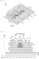
- FIG. 15 is a plan view showing a layer of the insulating substrate 1, the conductors 3b, according to Embodiment 3.
- FIG. 16 is a cross-sectional view taken along the line A1-A1 shown in FIG. 15, and
- FIG. 17 is a cross-sectional view taken along a line B-B shown in FIG. 15 .
- a plurality of conductors 3a, the non-connected conductor 30, the insulating plate 2a, and the connection conductors 4a according to Embodiment 3 are the same as in Embodiment 1.
- the insulating plate 2b is not formed, and the protruding conductor 40 for connection to the non-connected conductor 30 is also not formed.
- a plurality of conductors 3b are formed, and the plurality of conductors 3b include non-connected conductors 31 electrically insulated from another conductor 3b.
- the non-connected conductors 31 are electrically insulated from the other conductor 3b and the connection conductors 4a.
- the non-connected conductors 31 are provided at four corners of the insulating substrate 1, but the number and positions of the non-connected conductors 31 can be changed as appropriate.
- the heat dissipation conductor 5 is connected to each of the plurality of non-connected conductors 31 in a manner of protruding from the other conductor 3b on a back surface BS1 side of the insulating plate 2a. That is, the heat dissipation conductor 5 is not connected to the conductor 3b other than the non-connected conductors 31. In other words, a total thickness of the non-connected conductor 31 and the heat dissipation conductor 5 is larger than a thickness of the conductor 3b other than the non-connected conductors 31.
- the conductor 3b other than the non-connected conductors 31 serves as a current path, and the non-connected conductor 31 and the heat dissipation conductor 5 constitute a heat dissipation path insulated from the current path.
- the connection conductors 4a may be provided at lower portions of some of the conductors 3a, and some of the conductors 3a and the non-connected conductors 31 may be connected to each other via the connection conductors 4a. Such a method can also improve heat dissipation.
- FIG. 18 shows the power conversion apparatus 100 using the insulating substrate 1 according to Embodiment 3.
- the heat dissipation conductors 5 are connected to the heat sink 300 via the base plate 200.
- the insulating substrate 1, a plurality of semiconductor chips CHP, and the bonding wires BW are also covered with the protective member 400.
- the protective member 400 is present between the conductor 3b serving as the current path and the non-connected conductors 31 and between the conductor 3b serving as the current path and the base plate 200, these members are electrically insulated.
- FIGS. 11 and 12 show the effects according to Embodiment 3.
- "Heat area” on the horizontal axis in FIGS. 11 and 12 indicates an area of the heat dissipation conductors 5 in a plan view (here, a total area of the four heat dissipation conductors 5).
- the parasitic inductance Ls is higher in Embodiment 3 than in Study Example 2 ( FIG. 3 ), but the parasitic inductance Ls is substantially the same in Embodiment 3 as that in Study Example 1 ( FIG. 1 ), which has a single-layer insulating substrate structure.
- Embodiment 3 can also provide the insulating substrate 1 capable of keeping the parasitic inductance Ls low and improving heat dissipation, and reliability of the power conversion apparatus 100 can be improved using such an insulating substrate 1.
- Embodiment 4 the insulating substrate 1 and the power conversion apparatus 100 according to Embodiment 4 will be described with reference to FIGS. 19 to 22 .
- differences from Embodiment 3 will be mainly described, and the description of points overlapping with Embodiment 3 will be omitted.
- the protruding conductor 40 described in Embodiment 1 is applied based on the insulating substrate 1 according to Embodiment 3.
- FIG. 19 is a plan view showing a layer of the insulating substrate 1, the conductors 3b, according to Embodiment 4.
- FIG. 20 is a cross-sectional view taken along the line A1-A1 shown in FIG. 19, and
- FIG. 21 is a cross-sectional view taken along the line B-B shown in FIG. 19 .
- the protruding conductor 40 is formed in the insulating plate 2a in a manner of being embedded in the insulating plate 2a and protruding from the back surface BS1 of the insulating plate 2a.
- the protruding conductor 40 is electrically connected to the non-connected conductor 30, and is electrically insulated from the conductor 3b, the non-connected conductors 31, and the heat dissipation conductors 5.
- a plurality of protruding conductors 40 as shown in FIG. 7 can be also applied in Embodiment 4.
- FIG. 22 shows the power conversion apparatus 100 using the insulating substrate 1 according to Embodiment 4.
- the heat dissipation conductors 5 are connected to the heat sink 300 via the base plate 200.
- the insulating substrate 1, a plurality of semiconductor chips CHP, and the bonding wires BW are also covered with the protective member 400.
- the protective member 400 is present between the protruding conductor 40 and the conductor 3b serving as a current path and between the protruding conductor 40 and the base plate 200, these members are electrically insulated.
- the protruding conductor 40 according to Embodiment 4 protrudes toward the base plate 200 to the same extent as the conductor 3b, the protruding conductor 40 only needs to protrude to such an extent that the protruding conductor 40 does not contact the base plate 200.
- Embodiment 4 substantially the same effects as those according to Embodiment 3 can be attained, and heat dissipation can be further improved due to presence of the protruding conductor 40. Therefore, reliability of the power conversion apparatus 100 can be further improved.
- the insulating substrate 1 is mounted only on back surfaces of the semiconductor chips CHP in the power conversion apparatus 100 according to Embodiments 1 to 4. Alternatively, the insulating substrate 1 may be mounted on top surfaces of semiconductor chips CHP as well.
- one insulating substrate 1 and the other insulating substrate 1 are arranged such that a plurality of conductors 3a face each other.
- Back surfaces of a plurality of semiconductor chips CHP are disposed on a plurality of conductors 3a of the one insulating substrate 1
- top surfaces of the plurality of semiconductor chips CHP are disposed on a plurality of conductors 3a of the other insulating substrate 1.
- at least one of the plurality of semiconductor chips CHP is provided on the non-connected conductor 30 of the one insulating substrate 1 and on the non-connected conductor 30 of the other insulating substrate 1.
- Each of the heat dissipation conductor 5 of the one insulating substrate 1 and the heat dissipation conductor 5 of the other insulating substrate 1 is connected to a respective one of the heat sinks 300 via the base plate 200.
- Two sets of insulating substrates 1 and the plurality of semiconductor chips CHP are covered with the protective member 400.
- the parasitic inductance Ls can be reduced even in a structure in which both surfaces of each of the semiconductor chips CHP are sandwiched by the two sets of insulating substrates 1. Since heat can be dissipated from both surfaces of each of the semiconductor chips CHP, heat dissipation can be further improved. Therefore, reliability of the power conversion apparatus 100 can be improved.
- the two sets of insulating substrates 1 may not have the same structure.
- a structure according to Embodiment 1 may be applied to the one insulating substrate 1
- a structure according to Embodiment 4 may be applied to the other insulating substrate 1.
- a combination of the two sets of insulating substrates 1 can be selected from structures according to Embodiments 1 to 4 as appropriate.
- the base plates 200 and the heat sinks 300 may not necessarily be provided when an amount of heat dissipation is sufficient.
Landscapes
- Structure Of Printed Boards (AREA)
- Inverter Devices (AREA)
- Cooling Or The Like Of Semiconductors Or Solid State Devices (AREA)
Abstract
Description
- The present invention relates to an insulating substrate and a power conversion apparatus, and more particularly to an insulating substrate for mounting a semiconductor chip and a power conversion apparatus using the insulating substrate.
- In recent years, a power semiconductor chip of SiC, GaN, or the like, using a compound semiconductor substrate having a wideband gap, has been developed, and a power conversion apparatus having the power semiconductor chip mounted thereon has started to be introduced into the market. Since the power semiconductor chip of SiC, GaN, or the like has a smaller conduction loss than that of a related-art Si power semiconductor chip, a cooling system of the power conversion apparatus can be simplified.
- Since the power semiconductor chip of SiC, GaN, or the like can be driven at a high frequency, passive components such as inductors or capacitors provided in the power conversion apparatus can be downsized. With these effects, it is possible to reduce an overall size of the power conversion apparatus.
- A parasitic inductance Ls of the power conversion apparatus becomes a problem during high-frequency driving. As shown in
FIG. 1 , a surge voltage ΔV is represented by a product of the parasitic inductance Ls and an amount of current per time unit (di/dt). The large parasitic inductance Ls causes the large surge voltage ΔV to be applied when the semiconductor chip is turned off, and also becomes a source of noise. For high-frequency driving, it is necessary to increase an off-speed of the semiconductor chip, but the surge voltage ΔV and the noise greatly affect the off-speed. - For example,
PTL 1 discloses an insulating substrate including an insulating plate, a top surface wiring conductor formed on a top surface of the insulating plate, and a back surface wiring conductor formed on a back surface of the insulating plate. A semiconductor chip is disposed on the top surface wiring conductor. Here,PTL 1 discloses a technique for reducing a parasitic inductance using a bridge terminal provided on the top surface wiring conductor due to an effect of proximity reverse conduction. - PTL 1:
JP2015-185630A - The inventors of the present application have studied structures according to Study Example 1 shown in
FIG. 2 and Study Example 2 shown inFIG. 3 aspower conversion apparatus 100 for compound semiconductor substrates. - As shown in
FIG. 2 , thepower conversion apparatus 100 according to Study Example 1 uses aninsulating substrate 1 including aninsulating plate 2a, a plurality ofconductors 3a formed on a top surface of theinsulating plate 2a, and aheat dissipation conductor 5 formed on a back surface of theinsulating plate 2a. - A plurality of semiconductor chips CHP are disposed on the plurality of
conductors 3a, and the plurality ofconductors 3a and the plurality of semiconductor chips CHP are electrically connected by bonding wires BW as appropriate. Theheat dissipation conductor 5 is connected to aheat sink 300 via abase plate 200. - As shown in
FIG. 3 , thepower conversion apparatus 100 according to Study Example 2 further includes aconductor 3b and aninsulating plate 2b between theinsulating plate 2a and theheat dissipation conductor 5, thereby forming a multilayer insulating substrate structure. For this reason, in Study Example 2, since insulating plates and conductors through which a current flows are stacked for a plurality of layers, the parasitic inductance Ls can be reduced by mutual inductance as compared with Study Example 1. - However, in Study Example 2, since a distance from the semiconductor chips CHP as heat sources to a cooling system (heat sink 300) increases due to formation of the multilayer insulating substrate structure, a temperature of each of the semiconductor chips CHP tends to rise due to an increase in thermal resistance as compared with Study Example 1. As a result, a temperature difference between the maximum temperature and the minimum temperature increases, which makes the
conductor 3a to be likely to peel off from the semiconductor chip CHP. Similarly, peeling is likely to occur between theheat dissipation conductor 5 and thebase plate 200 and between thebase plate 200 and theheat sink 300. Not only the temperature of the semiconductor chip CHP but also a temperature of the entirepower conversion apparatus 100 tends to rise, and thus reliability of thepower conversion apparatus 100 may be lowered and a product life may be shortened. - Therefore, it is desirable to develop the
insulating substrate 1 capable of keeping the parasitic inductance Ls low and improving heat dissipation, thereby improving reliability of thepower conversion apparatus 100. Other problems and novel features will be apparent from the description of the present specification and the accompanying drawings. - Overviews of representative aspects in embodiments disclosed in the present application will be briefly described as follows.
- According to one aspect, there is provided an insulating substrate including: a first insulating plate including a top surface and a back surface; a second insulating plate formed on a back surface side of the first insulating plate and including a top surface and a back surface; a plurality of first conductors formed on the top surface of the first insulating plate; a second conductor formed between the back surface of the first insulating plate and the top surface of the second insulating plate; a heat dissipation conductor formed on the back surface of the second insulating plate and electrically insulated from the second conductor; and a plurality of first connection conductors formed inside the first insulating plate in a manner of electrically connecting some of the plurality of first conductors and the second conductor. Here, the plurality of first conductors include a first non-connected conductor that is not electrically connected to the second conductor via the plurality of first connection conductors, a protruding conductor is formed in the first insulating plate in a manner of being embedded in the first insulating plate and protruding from the back surface of the first insulating plate, and the protruding conductor is electrically connected to the first non-connected conductor, and is electrically insulated from the second conductor and the heat dissipation conductor.
- According to another aspect, there is provided an insulating substrate including: a first insulating plate including a top surface and a back surface; a plurality of first conductors formed on the top surface of the first insulating plate; a plurality of second conductors formed on the back surface of the first insulating plate; and a plurality of first connection conductors formed inside the first insulating plate in a manner of electrically connecting some of the plurality of first conductors and some of the plurality of second conductors. Here, the plurality of second conductors include a second non-connected conductor electrically insulated from another second conductor, and a heat dissipation conductor is connected to the second non-connected conductor in a manner of protruding from the other second conductor on a back surface side of the first insulating plate.
- According to the aspects, it is possible to provide an insulating substrate capable of keeping a parasitic inductance low and improving heat dissipation. Reliability of a power conversion apparatus can be improved using such an insulating substrate.
-
- [
FIG. 1] FIG. 1 is a graph showing a surge voltage during turn-off. - [
FIG. 2] FIG. 2 is a cross-sectional view showing an insulating substrate and a power conversion apparatus according to Study Example 1. - [
FIG. 3] FIG. 3 is a cross-sectional view showing an insulating substrate and a power conversion apparatus according to Study Example 2. - [
FIG. 4] FIG. 4 is a perspective view showing an insulating substrate according toEmbodiment 1. - [
FIG. 5] FIG. 5 is a cross-sectional view showing the insulating substrate according toEmbodiment 1. - [
FIG. 6] FIG. 6 is a plan view showing the inside of the insulating substrate according toEmbodiment 1. - [
FIG. 7] FIG. 7 is a plan view showing the inside of the insulating substrate according toEmbodiment 1. - [
FIG. 8] FIG. 8 is a perspective view showing a power conversion apparatus according toEmbodiment 1. - [
FIG. 9] FIG. 9 is a cross-sectional view showing the power conversion apparatus according toEmbodiment 1. - [
FIG. 10] FIG. 10 is a cross-sectional view showing the power conversion apparatus according toEmbodiment 1. - [
FIG. 11] FIG. 11 is a graph showing effects according toEmbodiment 1 andEmbodiment 3. - [
FIG. 12] FIG. 12 is a graph showing effects according toEmbodiment 1 andEmbodiment 3. - [
FIG. 13] FIG. 13 is a cross-sectional view showing an insulating substrate according toEmbodiment 2. - [
FIG. 14] FIG. 14 is a cross-sectional view showing a power conversion apparatus according toEmbodiment 2. - [
FIG. 15] FIG. 15 is a plan view showing the inside of an insulating substrate according toEmbodiment 3. - [
FIG. 16] FIG. 16 is a cross-sectional view showing the insulating substrate according toEmbodiment 3. - [
FIG. 17] FIG. 17 is a cross-sectional view showing the insulating substrate according toEmbodiment 3. - [
FIG. 18] FIG. 18 is a cross-sectional view showing a power conversion apparatus according toEmbodiment 3. - [
FIG. 19] FIG. 19 is a plan view showing the inside of an insulating substrate according to Embodiment 4. - [
FIG. 20] FIG. 20 is a cross-sectional view showing the insulating substrate according to Embodiment 4. - [
FIG. 21] FIG. 21 is a cross-sectional view showing the insulating substrate according to Embodiment 4. - [
FIG. 22] FIG. 22 is a cross-sectional view showing a power conversion apparatus according to Embodiment 4. - [
FIG. 23] FIG. 23 is a cross-sectional view showing a power conversion apparatus according to a modification. - [
FIG. 24] FIG. 24 is a cross-sectional view showing the power conversion apparatus according to the modification. - Hereinafter, embodiments of the invention will be described in detail with reference to the drawings. In all the drawings showing the embodiments, members having the same functions are denoted by the same reference numerals, and the repeated description thereof will be omitted. In the following embodiments, the description of the same or similar parts will not be repeated in principle unless particularly necessary.
- An X direction, a Y direction, and a Z direction described in the present application intersect with one another and are orthogonal to one another. In the present application, the Z direction is referred to as a vertical direction, an upper-lower direction, a height direction, or a thickness direction of a certain structure. An expression "plan view" used in the present application means viewing a plane formed by the X direction and the Y direction from the Z direction.
- Hereinafter, an insulating
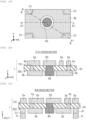
substrate 1 according toEmbodiment 1 will be described with reference toFIGS. 4 to 7 .FIG. 4 is a perspective view showing the insulatingsubstrate 1, andFIG. 5 is a cross-sectional view taken along a line A1-A1 shown inFIG. 4 .FIGS. 6 and 7 are plan views showing a layer of the insulatingsubstrate 1, aconductor 3b. - The insulating
substrate 1 includes a multilayer insulating substrate structure in which insulating plates and conductors through which a current flows are stacked for a plurality of layers. The insulatingsubstrate 1 includes an insulatingplate 2a, an insulatingplate 2b, a plurality ofconductors 3a, theconductor 3b, a plurality ofconnection conductors 4a, and aheat dissipation conductor 5. - The insulating
plate 2a includes a top surface TS1 and a back surface BS1. As shown inFIG. 4 , the plurality ofconductors 3a are formed on the top surface TS1 of the insulatingplate 2a. The plurality ofconductors 3a include anon-connected conductor 30. - As shown in
FIG. 5 , the insulatingplate 2b is formed on a back surface BS1 side of the insulatingplate 2a and has a top surface TS2 and a back surface BS2. Theconductor 3b is formed between the back surface BS1 of the insulatingplate 2a and the top surface TS2 of the insulatingplate 2b. The plurality ofconnection conductors 4a are formed in the insulatingplate 2a in a manner of electrically connecting some of the plurality ofconductors 3a and theconductor 3b. Theheat dissipation conductor 5 electrically insulated from theconductor 3b is formed on the back surface BS2 of the insulatingplate 2b. - As will be described later, various electronic devices such as a plurality of semiconductor chips, capacitors, and inductors are disposed on the plurality of
conductors 3a, and electrical conduction among the electronic devices is formed and a current path is constructed by electrically connecting the plurality ofconductors 3a, the plurality ofconnection conductors 4a, and theconductor 3b. A case where oneconductor 3b is provided is illustrated here. Alternatively, a plurality ofconductors 3b may be provided. In this case, a more complicated circuit can be constructed by the plurality ofconductors 3b. - In the insulating
substrate 1 according toEmbodiment 1, since the current path is multi-layered, a parasitic inductance Ls can be reduced by mutual inductance. - As described above, when a plurality of semiconductor chips are disposed on the plurality of
conductors 3a, the insulatingsubstrate 1 has a multilayer insulating substrate structure. Therefore, a distance between the plurality of semiconductor chips and theheat dissipation conductor 5 may increase, and heat dissipation may tend to deteriorate. - Here, the plurality of
conductors 3a include thenon-connected conductor 30 that is not electrically connected to theconductor 3b via the plurality ofconnection conductors 4a. Since a heat dissipation path electrically insulated from the current path is provided below thenon-connected conductor 30, heat dissipation can be improved. - As shown in
FIG. 5 , a protrudingconductor 40 is formed in the insulatingplate 2a in a manner of being embedded in the insulatingplate 2a and protruding from the back surface BS1 of the insulatingplate 2a. The protrudingconductor 40 is electrically connected to thenon-connected conductor 30, and is electrically insulated from theheat dissipation conductor 5 by the insulatingplate 2b. - As shown in
FIGS. 5 and 6 , the protrudingconductor 40 is electrically insulated from theconductor 3b by an insulatinglayer 41 surrounding the protrudingconductor 40 in a plan view. By using such a protrudingconductor 40 as a heat dissipation path independent of an electric path formed by theconductor 3b or the like, the parasitic inductance Ls can be kept low, and heat dissipation can be improved. - A plurality of protruding
conductors 40 may be provided as shown inFIG. 7 instead of only one as shown inFIG 6 . InFIG. 7 , the plurality of protrudingconductors 40 are formed in the insulatingplate 2a. Each of the plurality of protrudingconductors 40 is electrically connected to thenon-connected conductor 30, electrically insulated from theconductor 3b by the insulatinglayer 41, and electrically insulated from theheat dissipation conductor 5 by the insulatingplate 2b. - In a case in
FIG. 7 , a planar area of each protrudingconductor 40 is smaller than that inFIG. 6 , but heat dissipation can be ensured substantially the same inFIG. 7 as that inFIG. 6 when a total planar area of the plurality of protrudingconductors 40 is designed to be substantially the same as that inFIG. 6 . - The plurality of
conductors 3a including thenon-connected conductor 30, theconductor 3b, theheat dissipation conductor 5, the plurality ofconnection conductors 4a, and the protrudingconductor 40 are made of, for example, a metal material containing copper (Cu) or aluminum (Al). The insulatingplate 2a and the insulatingplate 2b are made of, for example, a ceramic or resin material. - Hereinafter, a
power conversion apparatus 100 according toEmbodiment 1 will be described with reference toFIGS. 8 to 10 .FIG. 8 is a perspective view showing thepower conversion apparatus 100, andFIGS. 9 and10 are cross-sectional views taken along a line A2-A2 shown inFIG 8 . The line A2-A2 is located on the same straight line as the line A1-A1 shown inFIGS. 4 and6 . - The
power conversion apparatus 100 includes the insulatingsubstrate 1, a plurality of semiconductor chips CHP, bonding wires BW, abase plate 200 and aheat sink 300. - As shown in
FIGS. 8 and 9 , theheat sink 300 is connected to theheat dissipation conductor 5 via thebase plate 200. Here, theheat dissipation conductor 5 and thebase plate 200 are connected to each other via a thermal interface material (TIM). Thebase plate 200 and theheat sink 300 are also connected via a TIM. The TIM is, for example, a material such as solder or a sintered material. Each of the plurality of semiconductor chips CHP has a top surface and a back surface, and back surfaces of the plurality of semiconductor chips CHP are disposed on the plurality ofconductors 3a by a TIM. At least one of the plurality of semiconductor chips CHP is provided on thenon-connected conductor 30. The plurality of semiconductor chips CHP and the plurality ofconductors 3a are electrically connected to each other by the bonding wires BW as appropriate. - Although not particularly shown, in addition to the plurality of semiconductor chips CHP, other electronic devices such as capacitors and inductors may be disposed on the plurality of
conductors 3a. - As shown in
FIG. 10 , in thepower conversion apparatus 100, the insulatingsubstrate 1, the plurality of semiconductor chips CHP, and the bonding wires BW may be covered with aprotective member 400. This can prevent the insulatingsubstrate 1, the semiconductor chips CHP, and the bonding wires BW from discharging with an external environment. Theprotective member 400 is made of an insulating material, and is made of, for example, an insulating gel or a molding resin. - The semiconductor chip CHP includes, for example, a compound semiconductor substrate of silicon carbide (SiC), gallium nitride (GaN), gallium oxide (Ga2O3), or the like, and a transistor such as a MOSFET formed on the compound semiconductor substrate.
- The bonding wire BW is made of, for example, a metal material containing gold (Au), copper (Cu), or aluminum (Al). The plurality of semiconductor chips CHP and the plurality of
conductors 3a may be electrically connected by ribbons, bus bars, or the like instead of the bonding wires BW. - The
base plate 200 is made of, for example, a composite material (AlSiC) in which SiC ceramic particles are contained in copper (Cu) or an aluminum alloy, or a composite material (MgSiC) in which SiC ceramic particles are contained in magnesium. Theheat sink 300 is made of, for example, a metal material containing copper (Cu), iron (Fe), or aluminum. -
FIGS. 11 and 12 are graphs showing effects according toEmbodiment 1, and are simulation results measured by the inventors of the present application.FIGS. 11 and 12 also show effects according toEmbodiment 3 described later. InEmbodiment 1, "Heat area" on a horizontal axis inFIGS. 11 and 12 indicates an area of the protrudingconductor 40 in a plan view. - As shown in
FIGS. 11 and 12 , in thepower conversion apparatus 100 according toEmbodiment 1, a temperature rise can be prevented as compared with Study Example 2 (FIG. 3 ), and the parasitic inductance Ls can be maintained to be substantially the same as that in Study Example 2 (FIG. 3 ). That is, according toEmbodiment 1, it is possible to provide the insulatingsubstrate 1 capable of keeping the parasitic inductance Ls low and improving heat dissipation, and reliability of thepower conversion apparatus 100 can be improved using such an insulatingsubstrate 1. - Hereinafter, the insulating
substrate 1 and thepower conversion apparatus 100 according toEmbodiment 2 will be described with reference toFIGS. 13 and14 . In the following description, differences fromEmbodiment 1 will be mainly described, and the description of points overlapping withEmbodiment 1 will be omitted. - As compared with
Embodiment 1, the insulatingsubstrate 1 according toEmbodiment 2 has a multilayer insulating substrate structure in which more insulating plates and conductors are stacked between the insulatingplate 2b and theheat dissipation conductor 5. - As shown in
FIG. 13 , an insulatingplate 2c including a top surface TS3 and a back surface BS3 is formed between the insulatingplate 2b and theheat dissipation conductor 5. Aconductor 3c is formed between the back surface BS2 of the insulatingplate 2b and the top surface TS3 of the insulatingplate 2c. A plurality ofconnection conductors 4b are formed in the insulatingplate 2b in a manner of electrically connecting theconductor 3b and theconductor 3c. The protrudingconductor 40 penetrates the insulatingplate 2b, protrudes from the back surface of the insulatingplate 2b, and is electrically insulated from theconductor 3c and theconnection conductors 4b. - As described above, in
Embodiment 2, a structure including the insulatingplate 2c, theconductor 3c, the plurality ofconnection conductors 4b, and the protrudingconductor 40 is repeatedly formed once or more from the insulatingplate 2b to theheat dissipation conductor 5. For example, when the structure is repeatedly formed twice, aconductor 3d,connection conductors 4c, and the like shown inFIG. 13 are formed. -
FIG. 14 shows thepower conversion apparatus 100 using the insulatingsubstrate 1 according toEmbodiment 2. InEmbodiment 2, the insulatingsubstrate 1 that is further multi-layered, a plurality of semiconductor chips CHP, and the bonding wires BW may also be covered with theprotective member 400. - Various electronic devices such as the plurality of semiconductor chips CHP, capacitors, and inductors are disposed on a plurality of
conductors 3a, but the insulatingsubstrate 1 is further multi-layered. Therefore, it is easier to freely design connection paths of these electronic devices, and a degree of freedom in circuit design can be increased. It is also easier to freely design a current path that reduces the parasitic inductor Ls. - Even when the insulating
substrate 1 is further multi-layered as described above, since the protrudingconductor 40 penetrates the insulating plates, a heat dissipation path can be ensured. Therefore, deterioration in heat dissipation can be prevented. Therefore, reliability of thepower conversion apparatus 100 using the insulatingsubstrate 1 can be improved. - Hereinafter, the insulating
substrate 1 and thepower conversion apparatus 100 according toEmbodiment 3 will be described with reference toFIGS. 15 to 18 . In the following description, differences fromEmbodiment 1 will be mainly described, and the description of points overlapping withEmbodiment 1 will be omitted. - In
Embodiment 1, when the insulatingsubstrate 1 has the multilayer insulating substrate structure, heat dissipation is improved by connecting the protrudingconductor 40 to thenon-connected conductor 30. InEmbodiment 3, when the insulatingsubstrate 1 has a single-layer insulating substrate structure, heat dissipation is improved by other devices. -
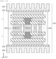
FIG. 15 is a plan view showing a layer of the insulatingsubstrate 1, theconductors 3b, according toEmbodiment 3.FIG. 16 is a cross-sectional view taken along the line A1-A1 shown inFIG. 15, and FIG. 17 is a cross-sectional view taken along a line B-B shown inFIG. 15 . - As shown in
FIG. 16 , a plurality ofconductors 3a, thenon-connected conductor 30, the insulatingplate 2a, and theconnection conductors 4a according toEmbodiment 3 are the same as inEmbodiment 1. However, inEmbodiment 3, the insulatingplate 2b is not formed, and the protrudingconductor 40 for connection to thenon-connected conductor 30 is also not formed. - As shown in
FIGS. 15 and 17 , inEmbodiment 3, a plurality ofconductors 3b are formed, and the plurality ofconductors 3b includenon-connected conductors 31 electrically insulated from anotherconductor 3b. Thenon-connected conductors 31 are electrically insulated from theother conductor 3b and theconnection conductors 4a. Here, thenon-connected conductors 31 are provided at four corners of the insulatingsubstrate 1, but the number and positions of thenon-connected conductors 31 can be changed as appropriate. - The
heat dissipation conductor 5 is connected to each of the plurality ofnon-connected conductors 31 in a manner of protruding from theother conductor 3b on a back surface BS1 side of the insulatingplate 2a. That is, theheat dissipation conductor 5 is not connected to theconductor 3b other than thenon-connected conductors 31. In other words, a total thickness of thenon-connected conductor 31 and theheat dissipation conductor 5 is larger than a thickness of theconductor 3b other than thenon-connected conductors 31. - As described above, in
Embodiment 3, theconductor 3b other than thenon-connected conductors 31 serves as a current path, and thenon-connected conductor 31 and theheat dissipation conductor 5 constitute a heat dissipation path insulated from the current path. - Since the
non-connected conductors 31 are electrically insulated from the plurality ofconductors 3a, the plurality ofconductors 3a can be freely arranged above thenon-connected conductors 31. By increasing an arrangement area of the plurality ofconductors 3a, heat dissipation from a top surface TS1 side of the insulatingplate 2a can be improved. When some of the plurality ofconductors 3a are not provided in the current path, theconnection conductors 4a may be provided at lower portions of some of theconductors 3a, and some of theconductors 3a and thenon-connected conductors 31 may be connected to each other via theconnection conductors 4a. Such a method can also improve heat dissipation. -
FIG. 18 shows thepower conversion apparatus 100 using the insulatingsubstrate 1 according toEmbodiment 3. Theheat dissipation conductors 5 are connected to theheat sink 300 via thebase plate 200. InEmbodiment 3, the insulatingsubstrate 1, a plurality of semiconductor chips CHP, and the bonding wires BW are also covered with theprotective member 400. - Here, since the
protective member 400 is present between theconductor 3b serving as the current path and thenon-connected conductors 31 and between theconductor 3b serving as the current path and thebase plate 200, these members are electrically insulated. -
FIGS. 11 and 12 show the effects according toEmbodiment 3. InEmbodiment 3, "Heat area" on the horizontal axis inFIGS. 11 and 12 indicates an area of theheat dissipation conductors 5 in a plan view (here, a total area of the four heat dissipation conductors 5). - As shown in
FIGS. 11 and 12 , in thepower conversion apparatus 100 according toEmbodiment 3, a temperature rise can be prevented as compared with Study Example 2 (FIG. 3 ). Meanwhile, since the insulatingsubstrate 1 according toEmbodiment 3 basically has the single-layer insulating substrate structure, the parasitic inductance Ls is higher inEmbodiment 3 than in Study Example 2 (FIG. 3 ), but the parasitic inductance Ls is substantially the same inEmbodiment 3 as that in Study Example 1 (FIG. 1 ), which has a single-layer insulating substrate structure. - That is,
Embodiment 3 can also provide the insulatingsubstrate 1 capable of keeping the parasitic inductance Ls low and improving heat dissipation, and reliability of thepower conversion apparatus 100 can be improved using such an insulatingsubstrate 1. - Hereinafter, the insulating
substrate 1 and thepower conversion apparatus 100 according to Embodiment 4 will be described with reference toFIGS. 19 to 22 . In the following description, differences fromEmbodiment 3 will be mainly described, and the description of points overlapping withEmbodiment 3 will be omitted. - In Embodiment 4, the protruding
conductor 40 described inEmbodiment 1 is applied based on the insulatingsubstrate 1 according toEmbodiment 3. -
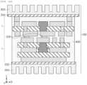
FIG. 19 is a plan view showing a layer of the insulatingsubstrate 1, theconductors 3b, according to Embodiment 4.FIG. 20 is a cross-sectional view taken along the line A1-A1 shown inFIG. 19, and FIG. 21 is a cross-sectional view taken along the line B-B shown inFIG. 19 . - As shown in
FIGS. 19 to 21 , the protrudingconductor 40 is formed in the insulatingplate 2a in a manner of being embedded in the insulatingplate 2a and protruding from the back surface BS1 of the insulatingplate 2a. The protrudingconductor 40 is electrically connected to thenon-connected conductor 30, and is electrically insulated from theconductor 3b, thenon-connected conductors 31, and theheat dissipation conductors 5. A plurality of protrudingconductors 40 as shown inFIG. 7 can be also applied in Embodiment 4. -
FIG. 22 shows thepower conversion apparatus 100 using the insulatingsubstrate 1 according to Embodiment 4. Theheat dissipation conductors 5 are connected to theheat sink 300 via thebase plate 200. In Embodiment 4, the insulatingsubstrate 1, a plurality of semiconductor chips CHP, and the bonding wires BW are also covered with theprotective member 400. - Here, since the
protective member 400 is present between the protrudingconductor 40 and theconductor 3b serving as a current path and between the protrudingconductor 40 and thebase plate 200, these members are electrically insulated. Although the protrudingconductor 40 according to Embodiment 4 protrudes toward thebase plate 200 to the same extent as theconductor 3b, the protrudingconductor 40 only needs to protrude to such an extent that the protrudingconductor 40 does not contact thebase plate 200. - As described above, according to Embodiment 4, substantially the same effects as those according to
Embodiment 3 can be attained, and heat dissipation can be further improved due to presence of the protrudingconductor 40. Therefore, reliability of thepower conversion apparatus 100 can be further improved. - Hereinafter, the
power conversion apparatus 100 according to a modification ofEmbodiments 1 to 4 will be described with reference toFIGS. 23 and24 . - The insulating
substrate 1 is mounted only on back surfaces of the semiconductor chips CHP in thepower conversion apparatus 100 according toEmbodiments 1 to 4. Alternatively, the insulatingsubstrate 1 may be mounted on top surfaces of semiconductor chips CHP as well. - As shown in
FIG. 23 , one insulatingsubstrate 1 and the other insulatingsubstrate 1 are arranged such that a plurality ofconductors 3a face each other. Back surfaces of a plurality of semiconductor chips CHP are disposed on a plurality ofconductors 3a of the one insulatingsubstrate 1, and top surfaces of the plurality of semiconductor chips CHP are disposed on a plurality ofconductors 3a of the other insulatingsubstrate 1. Here, at least one of the plurality of semiconductor chips CHP is provided on thenon-connected conductor 30 of the one insulatingsubstrate 1 and on thenon-connected conductor 30 of the other insulatingsubstrate 1. - Each of the
heat dissipation conductor 5 of the one insulatingsubstrate 1 and theheat dissipation conductor 5 of the other insulatingsubstrate 1 is connected to a respective one of theheat sinks 300 via thebase plate 200. Two sets of insulatingsubstrates 1 and the plurality of semiconductor chips CHP are covered with theprotective member 400. - As described above, the parasitic inductance Ls can be reduced even in a structure in which both surfaces of each of the semiconductor chips CHP are sandwiched by the two sets of insulating
substrates 1. Since heat can be dissipated from both surfaces of each of the semiconductor chips CHP, heat dissipation can be further improved. Therefore, reliability of thepower conversion apparatus 100 can be improved. - The two sets of insulating
substrates 1 may not have the same structure. For example, as shown inFIG. 24 , a structure according toEmbodiment 1 may be applied to the one insulatingsubstrate 1, and a structure according to Embodiment 4 may be applied to the other insulatingsubstrate 1. As described above, a combination of the two sets of insulatingsubstrates 1 can be selected from structures according toEmbodiments 1 to 4 as appropriate. - In the
power conversion apparatus 100 using the two sets of insulatingsubstrates 1, since heat can be dissipated from both surfaces of each of the semiconductor chips CHP, thebase plates 200 and theheat sinks 300 may not necessarily be provided when an amount of heat dissipation is sufficient. - Although the invention has been specifically described based on the above embodiments, the invention is not limited to the above embodiments, and various modifications can be made without departing from the scope of the invention.
-
- 1: insulating substrate
- 2a to 2c: insulating plate
- 3a to 3d: conductor
- 4a to 4c: connection conductor
- 5: heat dissipation conductor
- 30, 31: non-connected conductor
- 40: protruding conductor
- 41: insulating layer
- 100: power conversion apparatus
- 200: base plate
- 300: heat sink
- 400: protective member
- BS1 to BS3: back surface
- BW: bonding wire
- CHP: semiconductor chip
- TS1 to TS3: top surface
Claims (15)
- An insulating substrate comprising:a first insulating plate including a top surface and a back surface;a second insulating plate formed on a back surface side of the first insulating plate and including a top surface and a back surface;a plurality of first conductors formed on the top surface of the first insulating plate;a second conductor formed between the back surface of the first insulating plate and the top surface of the second insulating plate;a heat dissipation conductor formed on the back surface of the second insulating plate and electrically insulated from the second conductor; anda plurality of first connection conductors formed inside the first insulating plate in a manner of electrically connecting some of the plurality of first conductors and the second conductor, whereinthe plurality of first conductors include a first non-connected conductor that is not electrically connected to the second conductor via the plurality of first connection conductors,a protruding conductor is formed in the first insulating plate in a manner of being embedded in the first insulating plate and protruding from the back surface of the first insulating plate, andthe protruding conductor is electrically connected to the first non-connected conductor, and is electrically insulated from the second conductor and the heat dissipation conductor.
- The insulating substrate according to claim 1, whereina plurality of the protruding conductors are formed in the first insulating plate, andeach of the plurality of protruding conductors is electrically connected to the first non-connected conductor, and is electrically insulated from the second conductor and the heat dissipation conductor.
- The insulating substrate according to claim 1, further comprising:a third insulating plate formed between the second insulating plate and the heat dissipation conductor and including a top surface and a back surface;a third conductor formed between the back surface of the second insulating plate and the top surface of the third insulating plate; anda plurality of second connection conductors formed inside the second insulating plate in a manner of electrically connecting the second conductor and the third conductor, whereinthe protruding conductor penetrates the second insulating plate, protrudes from the back surface of the second insulating plate, and is electrically insulated from the third conductor and the second connection conductors, anda structure including the third insulating plate, the third conductor, the plurality of second connection conductors, and the protruding conductor is repeatedly formed once or more from the second insulating plate to the heat dissipation conductor.
- A power conversion apparatus using the insulating substrate according to claim 1, the power conversion apparatus comprising:a plurality of semiconductor chips each including a top surface and a back surface; anda heat sink connected to the heat dissipation conductor via a base plate, whereinback surfaces of the plurality of semiconductor chips are disposed on the plurality of first conductors, andat least one of the plurality of semiconductor chips is provided on the first non-connected conductor.
- A power conversion apparatus using the insulating substrate according to claim 1, the power conversion apparatus comprising:a plurality of semiconductor chips each including a top surface and a back surface; andtwo sets of the insulating substrates, whereinone insulating substrate and the other insulating substrate are arranged such that the plurality of first conductors face each other,back surfaces of the plurality of semiconductor chips are disposed on a plurality of the first conductors of the one insulating substrate,top surfaces of the plurality of semiconductor chips are disposed on a plurality of the first conductors of the other insulating substrate, andat least one of the plurality of semiconductor chips is provided on the first non-connected conductor of the one insulating substrate and on the first non-connected conductor of the other insulating substrate.
- The power conversion apparatus according to claim 5, wherein
a heat sink is connected to each of the heat dissipation conductor of the one insulating substrate and the heat dissipation conductor of the other insulating substrate via a base plate. - The power conversion apparatus according to claim 4, wherein
each of the plurality of semiconductor chips includes a compound semiconductor substrate and a transistor formed on the compound semiconductor substrate. - An insulating substrate comprising:a first insulating plate including a top surface and a back surface;a plurality of first conductors formed on the top surface of the first insulating plate;a plurality of second conductors formed on the back surface of the first insulating plate; anda plurality of first connection conductors formed inside the first insulating plate in a manner of electrically connecting some of the plurality of first conductors and some of the plurality of second conductors, whereinthe plurality of second conductors include a second non-connected conductor electrically insulated from another second conductor, anda heat dissipation conductor is connected to the second non-connected conductor in a manner of protruding from the other second conductor on a back surface side of the first insulating plate.
- The insulating substrate according to claim 8, whereinthe plurality of second conductors include a plurality of the second non-connected conductors, andeach of the plurality of second non-connected conductors is connected to the heat dissipation conductor.
- The insulating substrate according to claim 8, whereinthe plurality of first conductors include a first non-connected conductor that is not electrically connected to the plurality of second conductors via the plurality of first connection conductors,a protruding conductor is formed in the first insulating plate in a manner of being embedded in the first insulating plate and protruding from the back surface of the first insulating plate, andthe protruding conductor is electrically connected to the first non-connected conductor, and is electrically insulated from the plurality of second conductors, the second non-connected conductor, and the heat dissipation conductor.
- The insulating substrate according to claim 10, whereina plurality of the protruding conductors are formed in the first insulating plate, andeach of the plurality of protruding conductors is electrically connected to the first non-connected conductor, and is electrically insulated from the plurality of second conductors and the heat dissipation conductor.
- A power conversion apparatus using the insulating substrate according to claim 8, the power conversion apparatus comprising:a plurality of semiconductor chips each including a top surface and a back surface; anda heat sink connected to the heat dissipation conductor via a base plate, whereinback surfaces of the plurality of semiconductor chips are disposed on the plurality of first conductors.
- A power conversion apparatus using the insulating substrate according to claim 8, the power conversion apparatus comprising:a plurality of semiconductor chips each including a top surface and a back surface; andtwo sets of the insulating substrates, whereinone insulating substrate and the other insulating substrate are arranged such that the plurality of first conductors face each other,back surfaces of the plurality of semiconductor chips are disposed on a plurality of the first conductors of the one insulating substrate, andtop surfaces of the plurality of semiconductor chips are disposed on a plurality of the first conductors of the other insulating substrate.
- The power conversion apparatus according to claim 13, wherein
a heat sink is connected to each of the heat dissipation conductor of the one insulating substrate and the heat dissipation conductor of the other insulating substrate via a base plate. - The power conversion apparatus according to claim 12, wherein
each of the plurality of semiconductor chips includes a compound semiconductor substrate and a transistor formed on the compound semiconductor substrate.
Applications Claiming Priority (2)
| Application Number | Priority Date | Filing Date | Title |
|---|---|---|---|
| JP2020200810A JP7535444B2 (en) | 2020-12-03 | 2020-12-03 | Insulating substrate and power conversion device |
| PCT/JP2021/032188 WO2022118510A1 (en) | 2020-12-03 | 2021-09-01 | Insulated board and power converter |
Publications (3)
| Publication Number | Publication Date |
|---|---|
| EP4258337A1 true EP4258337A1 (en) | 2023-10-11 |
| EP4258337A4 EP4258337A4 (en) | 2024-10-09 |
| EP4258337B1 EP4258337B1 (en) | 2025-12-24 |
Family
ID=81852691
Family Applications (1)
| Application Number | Title | Priority Date | Filing Date |
|---|---|---|---|
| EP21900266.4A Active EP4258337B1 (en) | 2020-12-03 | 2021-09-01 | Insulated board and power converter |
Country Status (3)
| Country | Link |
|---|---|
| EP (1) | EP4258337B1 (en) |
| JP (1) | JP7535444B2 (en) |
| WO (1) | WO2022118510A1 (en) |
Families Citing this family (1)
| Publication number | Priority date | Publication date | Assignee | Title |
|---|---|---|---|---|
| CN115580225A (en) * | 2022-11-04 | 2023-01-06 | 大庆华研环保应用技术研发中心有限公司 | A heat dissipation structure for a concentrated photovoltaic cell substrate |
Family Cites Families (7)
| Publication number | Priority date | Publication date | Assignee | Title |
|---|---|---|---|---|
| JP5250707B2 (en) * | 2011-05-26 | 2013-07-31 | 有限会社 ナプラ | Electronic equipment substrate and electronic equipment |
| EP2991106A1 (en) * | 2013-04-24 | 2016-03-02 | Fuji Electric Co., Ltd. | Power semiconductor module and method for manufacturing same, and power converter |
| DE112014001487B4 (en) * | 2013-10-03 | 2021-03-04 | Fuji Electric Co., Ltd. | Semiconductor module |
| JP6331543B2 (en) * | 2014-03-24 | 2018-05-30 | 日産自動車株式会社 | Half-bridge power semiconductor module and manufacturing method thereof |
| CN106489203B (en) * | 2014-07-03 | 2018-09-18 | 日产自动车株式会社 | Semibridge system power semiconductor modular and its manufacturing method |
| JP2019046899A (en) * | 2017-08-31 | 2019-03-22 | ルネサスエレクトロニクス株式会社 | Electronic device |
| FR3084960B1 (en) * | 2018-08-07 | 2020-10-23 | Safran Electrical & Power | ELECTRICAL POWER CIRCUIT FOR ELECTRIC POWER CONVERTER |
-
2020
- 2020-12-03 JP JP2020200810A patent/JP7535444B2/en active Active
-
2021
- 2021-09-01 EP EP21900266.4A patent/EP4258337B1/en active Active
- 2021-09-01 WO PCT/JP2021/032188 patent/WO2022118510A1/en not_active Ceased
Also Published As
| Publication number | Publication date |
|---|---|
| JP2022088783A (en) | 2022-06-15 |
| EP4258337B1 (en) | 2025-12-24 |
| JP7535444B2 (en) | 2024-08-16 |
| WO2022118510A1 (en) | 2022-06-09 |
| EP4258337A4 (en) | 2024-10-09 |
Similar Documents
| Publication | Publication Date | Title |
|---|---|---|
| US7786486B2 (en) | Double-sided package for power module | |
| US11527456B2 (en) | Power module with organic layers | |
| CN102593081B (en) | Comprise the semiconductor device of radiator | |
| Dietrich | Trends in automotive power semiconductor packaging | |
| US9385107B2 (en) | Multichip device including a substrate | |
| EP4128341B1 (en) | Multi-chip package with reinforced isolation | |
| CN114008774A (en) | Electronic circuit and method for producing an electronic circuit | |
| US20230240012A1 (en) | Power electronic assembly having a laminate inlay and method of producing the power electronic assembly | |
| EP2889902B1 (en) | Electric power semiconductor device | |
| KR102905151B1 (en) | Electronic packages with integrated heat spreaders | |
| JP2007234690A (en) | Power semiconductor module | |
| WO2022213013A1 (en) | Double-side cooled power modules with sintered-silver interposers | |
| JPWO2012081434A1 (en) | Semiconductor device | |
| EP4258337B1 (en) | Insulated board and power converter | |
| EP3410481A1 (en) | Power semiconductor chip module | |
| CN112530915A (en) | Semiconductor device with a plurality of semiconductor chips | |
| JP2023134143A (en) | Semiconductor modules, semiconductor devices, and vehicles | |
| EP4084062A1 (en) | Power semiconductor module arrangement | |
| Bäumler et al. | Reliability aspects of 3D integrated power devices | |
| US11521921B2 (en) | Semiconductor device package assemblies and methods of manufacture | |
| US20250380362A1 (en) | Circuit assembly with two circuit carriers and a semiconductor component | |
| CN111584422A (en) | Semiconductor device and method of manufacturing the same | |
| KR20230136459A (en) | Power semiconductor module and method for manufacturing thereof | |
| JP2009064904A (en) | Copper circuit board and semiconductor module device using the same | |
| CN114615857A (en) | Heat dissipation for power switches |
Legal Events
| Date | Code | Title | Description |
|---|---|---|---|
| STAA | Information on the status of an ep patent application or granted ep patent |
Free format text: STATUS: THE INTERNATIONAL PUBLICATION HAS BEEN MADE |
|
| PUAI | Public reference made under article 153(3) epc to a published international application that has entered the european phase |
Free format text: ORIGINAL CODE: 0009012 |
|
| STAA | Information on the status of an ep patent application or granted ep patent |
Free format text: STATUS: REQUEST FOR EXAMINATION WAS MADE |
|
| 17P | Request for examination filed |
Effective date: 20230703 |
|
| AK | Designated contracting states |
Kind code of ref document: A1 Designated state(s): AL AT BE BG CH CY CZ DE DK EE ES FI FR GB GR HR HU IE IS IT LI LT LU LV MC MK MT NL NO PL PT RO RS SE SI SK SM TR |
|
| DAV | Request for validation of the european patent (deleted) | ||
| DAX | Request for extension of the european patent (deleted) | ||
| REG | Reference to a national code |
Ref country code: DE Ref legal event code: R079 Free format text: PREVIOUS MAIN CLASS: H01L0023120000 Ipc: H01L0023373000 Ref country code: DE Ref legal event code: R079 Ref document number: 602021045224 Country of ref document: DE Free format text: PREVIOUS MAIN CLASS: H01L0023120000 Ipc: H01L0023373000 |
|
| A4 | Supplementary search report drawn up and despatched |
Effective date: 20240911 |
|
| RIC1 | Information provided on ipc code assigned before grant |
Ipc: H01L 23/48 20060101ALN20240905BHEP Ipc: H01L 25/16 20230101ALN20240905BHEP Ipc: H01L 23/31 20060101ALN20240905BHEP Ipc: H01L 23/051 20060101ALN20240905BHEP Ipc: H01L 23/538 20060101ALN20240905BHEP Ipc: H02M 7/00 20060101ALN20240905BHEP Ipc: H02M 1/32 20070101ALN20240905BHEP Ipc: H01L 25/18 20230101ALI20240905BHEP Ipc: H01L 25/07 20060101ALI20240905BHEP Ipc: H01L 23/367 20060101ALI20240905BHEP Ipc: H01L 23/373 20060101AFI20240905BHEP |
|
| STAA | Information on the status of an ep patent application or granted ep patent |
Free format text: STATUS: EXAMINATION IS IN PROGRESS |
|
| 17Q | First examination report despatched |
Effective date: 20250213 |
|
| RIC1 | Information provided on ipc code assigned before grant |
Ipc: H01L 23/373 20060101AFI20250801BHEP Ipc: H01L 23/367 20060101ALI20250801BHEP Ipc: H01L 25/07 20060101ALI20250801BHEP Ipc: H01L 25/18 20230101ALI20250801BHEP Ipc: H02M 1/32 20070101ALN20250801BHEP Ipc: H02M 7/00 20060101ALN20250801BHEP Ipc: H01L 23/538 20060101ALN20250801BHEP Ipc: H01L 23/051 20060101ALN20250801BHEP Ipc: H01L 23/31 20060101ALN20250801BHEP Ipc: H01L 25/16 20230101ALN20250801BHEP Ipc: H01L 23/48 20060101ALN20250801BHEP |
|
| GRAP | Despatch of communication of intention to grant a patent |
Free format text: ORIGINAL CODE: EPIDOSNIGR1 |
|
| STAA | Information on the status of an ep patent application or granted ep patent |
Free format text: STATUS: GRANT OF PATENT IS INTENDED |
|
| INTG | Intention to grant announced |
Effective date: 20250919 |
|
| GRAS | Grant fee paid |
Free format text: ORIGINAL CODE: EPIDOSNIGR3 |
|
| GRAA | (expected) grant |
Free format text: ORIGINAL CODE: 0009210 |
|
| STAA | Information on the status of an ep patent application or granted ep patent |
Free format text: STATUS: THE PATENT HAS BEEN GRANTED |
|
| REG | Reference to a national code |
Ref country code: DE Ref legal event code: R079 Ref document number: 602021045224 Country of ref document: DE Free format text: PREVIOUS MAIN CLASS: H01L0023373000 Ipc: H10W0040250000 |
|
| AK | Designated contracting states |
Kind code of ref document: B1 Designated state(s): AL AT BE BG CH CY CZ DE DK EE ES FI FR GB GR HR HU IE IS IT LI LT LU LV MC MK MT NL NO PL PT RO RS SE SI SK SM TR |
|
| REG | Reference to a national code |
Ref country code: CH Ref legal event code: F10 Free format text: ST27 STATUS EVENT CODE: U-0-0-F10-F00 (AS PROVIDED BY THE NATIONAL OFFICE) Effective date: 20251224 Ref country code: GB Ref legal event code: FG4D |
|
| REG | Reference to a national code |
Ref country code: DE Ref legal event code: R096 Ref document number: 602021045224 Country of ref document: DE |
|
| REG | Reference to a national code |
Ref country code: LT Ref legal event code: MG9D |
|
| PG25 | Lapsed in a contracting state [announced via postgrant information from national office to epo] |
Ref country code: NO Free format text: LAPSE BECAUSE OF FAILURE TO SUBMIT A TRANSLATION OF THE DESCRIPTION OR TO PAY THE FEE WITHIN THE PRESCRIBED TIME-LIMIT Effective date: 20260324 |
|
| PG25 | Lapsed in a contracting state [announced via postgrant information from national office to epo] |
Ref country code: HR Free format text: LAPSE BECAUSE OF FAILURE TO SUBMIT A TRANSLATION OF THE DESCRIPTION OR TO PAY THE FEE WITHIN THE PRESCRIBED TIME-LIMIT Effective date: 20251224 Ref country code: FI Free format text: LAPSE BECAUSE OF FAILURE TO SUBMIT A TRANSLATION OF THE DESCRIPTION OR TO PAY THE FEE WITHIN THE PRESCRIBED TIME-LIMIT Effective date: 20251224 |
|
| PG25 | Lapsed in a contracting state [announced via postgrant information from national office to epo] |
Ref country code: RS Free format text: LAPSE BECAUSE OF FAILURE TO SUBMIT A TRANSLATION OF THE DESCRIPTION OR TO PAY THE FEE WITHIN THE PRESCRIBED TIME-LIMIT Effective date: 20260324 |
|
| PG25 | Lapsed in a contracting state [announced via postgrant information from national office to epo] |
Ref country code: LV Free format text: LAPSE BECAUSE OF FAILURE TO SUBMIT A TRANSLATION OF THE DESCRIPTION OR TO PAY THE FEE WITHIN THE PRESCRIBED TIME-LIMIT Effective date: 20251224 |
|
| REG | Reference to a national code |
Ref country code: NL Ref legal event code: MP Effective date: 20251224 |
|
| PG25 | Lapsed in a contracting state [announced via postgrant information from national office to epo] |
Ref country code: BG Free format text: LAPSE BECAUSE OF FAILURE TO SUBMIT A TRANSLATION OF THE DESCRIPTION OR TO PAY THE FEE WITHIN THE PRESCRIBED TIME-LIMIT Effective date: 20251224 |