EP4258314A2 - Circuit breaker and circuit breaking method - Google Patents
Circuit breaker and circuit breaking method Download PDFInfo
- Publication number
- EP4258314A2 EP4258314A2 EP23195006.4A EP23195006A EP4258314A2 EP 4258314 A2 EP4258314 A2 EP 4258314A2 EP 23195006 A EP23195006 A EP 23195006A EP 4258314 A2 EP4258314 A2 EP 4258314A2
- Authority
- EP
- European Patent Office
- Prior art keywords
- grid
- arc
- circuit breaker
- insulating portion
- contact
- Prior art date
- Legal status (The legal status is an assumption and is not a legal conclusion. Google has not performed a legal analysis and makes no representation as to the accuracy of the status listed.)
- Pending
Links
Images



Classifications
-
- H—ELECTRICITY
- H01—ELECTRIC ELEMENTS
- H01H—ELECTRIC SWITCHES; RELAYS; SELECTORS; EMERGENCY PROTECTIVE DEVICES
- H01H73/00—Protective overload circuit-breaking switches in which excess current opens the contacts by automatic release of mechanical energy stored by previous operation of a hand reset mechanism
- H01H73/02—Details
- H01H73/18—Means for extinguishing or suppressing arc
-
- H—ELECTRICITY
- H01—ELECTRIC ELEMENTS
- H01H—ELECTRIC SWITCHES; RELAYS; SELECTORS; EMERGENCY PROTECTIVE DEVICES
- H01H9/00—Details of switching devices, not covered by groups H01H1/00 - H01H7/00
- H01H9/30—Means for extinguishing or preventing arc between current-carrying parts
- H01H9/34—Stationary parts for restricting or subdividing the arc, e.g. barrier plate
- H01H9/36—Metal parts
-
- H—ELECTRICITY
- H01—ELECTRIC ELEMENTS
- H01H—ELECTRIC SWITCHES; RELAYS; SELECTORS; EMERGENCY PROTECTIVE DEVICES
- H01H9/00—Details of switching devices, not covered by groups H01H1/00 - H01H7/00
- H01H9/30—Means for extinguishing or preventing arc between current-carrying parts
- H01H9/34—Stationary parts for restricting or subdividing the arc, e.g. barrier plate
- H01H9/36—Metal parts
- H01H2009/365—Metal parts using U-shaped plates
-
- H—ELECTRICITY
- H01—ELECTRIC ELEMENTS
- H01H—ELECTRIC SWITCHES; RELAYS; SELECTORS; EMERGENCY PROTECTIVE DEVICES
- H01H9/00—Details of switching devices, not covered by groups H01H1/00 - H01H7/00
- H01H9/30—Means for extinguishing or preventing arc between current-carrying parts
- H01H9/46—Means for extinguishing or preventing arc between current-carrying parts using arcing horns
Definitions
- the present invention relates to a circuit breaker and a circuit breaking method, which include an arc chute arranged with grids.
- Patent document 1 discloses a circuit breaker in which a notched portion is provided at an arc approach portion of a grid to generate electromagnetic force that draws the arc into the grid by the action of biasing magnetic flux.
- Patent Document 1 JP-A-2006-12540
- the present invention has been made to solve the aforementioned problem, and an object of the present invention is to provide a circuit breaker and a circuit breaking method, which improve breaking performance by suppressing the return of the arc to the contact sides and maintaining a high arc voltage.
- circuit breaker and a circuit breaking method as defined in the independent claims are provided. Further embodiments of the claimed invention are defined in the dependent claims. Although the claimed invention is only defined by the claims, the below embodiments, examples, and aspects are present for aiding in understanding the background and advantages of the claimed invention.
- a circuit breaker includes: a fixed member having a fixed contact; a movable member having a movable contact that is connected to and disconnected from the fixed contact; and an arc chute arranged with a plurality of laminated grids, each of which has a notch portion into which an arc generated between the fixed contact and the movable contact is drawn and an insulating portion which is adjacent to a peak portion of the notch portion and is extended in a width direction.
- a circuit breaking method is a circuit breaking method of a circuit breaker in which an arc generated between contact is interrupted by at least one grid to extinguish the arc, the circuit breaking method comprising the steps of: drawing the arc generated between the contact into a state where the arc generates arc discharge s at mutually different positions of the grid and flows through the grid; and bypassing currents flowing the grid between those generated arc discharges by an insulating portion provided between those mutually different positions of the grid to extinguish the arc.
- the plurality of laminated grids are arranged in the arc chute, whereby it becomes possible to suppress the return of the arc to the contact sides and to improve breaking performance. Furthermore, according to the circuit breaking method of the present invention, the currents flowing between the arcs in which arc discharges are generated at the mutually different positions of the grid are made to bypass by the insulating portion, whereby it becomes possible to suppress the return of the arc to the contact sides and to improve breaking performance.
- FIG. 1 is a schematic configuration diagram showing a circuit breaker according to Embodiment 1 of the present invention.
- a circuit breaker 100 includes: a fixed member 1 having a fixed contact 1a; a movable member 2 having a movable contact 2a; a fixed member side arc horn 3 electrically connected to the fixed member 1; a movable member side arc horn 4 electrically connected to the movable member 2; and an arc chute 7 arranged with a plurality of grids 5 that interrupt an arc 10 and a plurality of support plates 6 that support the grids 5.
- the circuit breaker 100 is arranged with an upper conductor 11 and a lower conductor 12 below the arc chute 7.
- the upper conductor 11 and the lower conductor 12 are electrically connected to the fixed member 1 and the movable member 2, respectively.
- the fixed contact 1a is connected to and disconnected from the movable contact 2a, thereby energizing and breaking current between the upper conductor 11 and the lower conductor 12.
- An tripping device 13 connected to the lower conductor 12 detects overcurrent in breaking current and a latch 14 that holds the movable member 2 in energizing is released, whereby the movable member 2 is rotated in a direction away from the fixed member 1 to open the fixed contact 1a and the movable contact 2a. Furthermore, when the opened state is brought to the energizing state shown in FIG. 1 , an actuator 15 coupled to the movable member 2 drives the movable member 2 to a position where the movable contact 2a comes in contact with the fixed contact 1a.
- the fixed member side arc horn 3 is provided on an upper portion of the fixed member 1; and the movable member side arc horn 4 is provided on an upper portion of the movable member 2, the fixed member side arc horn 3 and the movable member side arc horn 4 being for guiding the arc 10 generated between the fixed contact 1a and the movable contact 2a (hereinafter, referred to as both contact 1a, 2a) to the arc chute 7.
- Each one end of the fixed member side arc horn 3 and the movable member side arc horn 4 is arranged adjacent to both contact 1a, 2a, respectively; and each other end thereof is provided in an extended manner so as to separate from each other.
- the arc chute 7 has the grid 5 formed of conductive plate-shaped metal and the insulating support plate 6 that supports the grid 5.
- the plurality of laminated grids 5 and support plates 6 are arranged with a predetermined distance on an upper portion of the fixed member side arc horn 3 and the movable member side arc horn 4.
- the support plate 6 is arranged on the bottom surface of the grid 5 to support the grid 5 and to prevent the arc 10 from jumping out to both contact 1a, 2a sides and from causing bridging.
- a top surface plate 8 is arranged on the uppermost tier of the grids 5. The top surface plate 8 prevents arc gas 20 generated by the heat of the arc 10 from leaking above the arc chute 7.
- An exhaust port 16 (not shown in the drawing) which is for discharging the arc gas 20 to the outside of the circuit breaker 100 is provided on both sides of the arc chute 7.
- FIG. 2 is a schematic configuration diagram showing an example of the grid of the circuit breaker according to Embodiment 1 of the present invention.
- the grid 5 has a notch portion 51 formed on one end portion and an insulating portion 52 which is adjacent to a peak portion 51a of the notch portion 51 and is extended in a width direction.
- a direction toward the notch portion 51 and a direction toward a top portion 53 opposite to the notch portion 51 are referred to as a length direction and a direction perpendicular to the length direction is referred to as a width direction.
- the insulating portion 52 is, for example, a slit-shaped through hole.
- the shape of the notch portion 51 is a V-shape, a U-shape, a rectangular shape, or the like.
- FIG. 3 is a schematic configuration diagram showing the grid and the support plate of the circuit breaker according to Embodiment 1 of the present invention.
- two grids 5 are arranged on the support plate 6 so that the notch portions 51 face to each other.
- the support plate 6 is formed with an opening portion 61 in the center thereof and the insulating portion 52 of the grid 5 is arranged so as to overlap on the opening portion 61 of the support plate 6.
- the support plate 6 is provided so that the center of the opening portion 61 is located at both contact 1a, 2a when seen from the upper side of FIG. 1 . That is, the grids 5 are arranged so that the notch portions 51 are directed toward both contacts 1a, 2a.
- the support plate 6 and the top surface plate 8 are formed of thermosetting resin such as unsaturated polyester resin and melamine resin and may be formed of ceramics such as alumina and zirconia as other material.
- FIG. 4 is a typical view showing an arc of the circuit breaker according to Embodiment 1 of the present invention.
- the circuit breaker 100 is opened the contacts by separating the movable member 2 from the fixed member 1 to generate the arc 10 between the fixed contact 1a and the movable contact 2a.
- the generated arc 10 is commutated to the fixed member side arc horn 3 or the movable member side arc horn 4 arranged on the upper portion of both contact 1a, 2a.
- the commutated arc 10 is guided to the arc chute 7 by electromagnetic force that is exerted by magnetic flux produced by current flowing through the fixed member side arc horn 3 or the movable member side arc horn 4 (hereinafter, referred to as both arc horns 3, 4).
- FIG. 5 is a typical view showing the action of the arc in the arc chute of the circuit breaker according to Embodiment 1 of the present invention.
- FIG. 5(a) is a top view of the grid; and
- FIG. 5(b) is a perspective view of the grid.
- electromagnetic force F exerts on the arc 10 by biasing magnetic flux ⁇ that passes through the grid 5 and the arc 10 is drawn into the notch portion 51 of the grid 5 in the arc chute 7.
- the arc 10 is driven toward the notch portion 51 of the grid 5 to come in contact with the grid 5.
- the arc 10 flows through in the thickness direction of the grid 5 and is interrupted by the plurality of grids 5 arranged in lamination.
- FIG. 6 is a typical view showing the action of the arc in the grid of the circuit breaker according to Embodiment 1 of the present invention.
- FIG. 6(a) is a perspective view of the grid; and
- FIG. 6(b) is a sectional view taken along the line A-A' of the grid.
- the arc 10 flowing through in the thickness direction of the grid 5 generates arc discharges at different positions of the plate surface of the grid 5 due to differences of time from generation between both contacts 1a, 2a to arrival at the plate surface of the grid 5, generation places of arc discharge on the grid 5, and the like. As shown in FIG.
- the arc 10c traces a current path that flows from the arc 10b on the top portion 53 side to the arc 10a on the notch portion 51 side, bypassing the insulating portion 52.
- FIG. 7 is a typical view for explaining the action of a grid according to Embodiment 1 of the present invention.
- FIG. 7 (a) is a perspective view of the grid; and
- FIG. 7(b) is a sectional view taken along the line B-B' of the grid.
- electromagnetic repulsive force P exerts between the arc 10c flowing straight from the top portion 53 side toward the notch portion 51 side along the plate surface of the grid 5 and the arcs 10a, 10b flowing through in the thickness direction of the grid 5.
- the arc 10a on the notch portion 51 side is drawn back to both contact 1a, 2a sides by the electromagnetic repulsive force P.
- FIG. 8 is a typical view showing a flow of arc gas according to Embodiment 1 of the present invention.
- the arc gas 20 generated at both contacts 1a, 2a flows from the opening portion 61 of the support plate 6 to a mutual gap 5d between the grids 5 arranged in lamination and is discharged from the exhaust port 16 arranged on both sides of the arc chute 7 to the outside of the circuit breaker 100.
- the insulating portion 52 of the grid 5 is the through hole, the arc gas 20 generated at both arc horns 3, 4 flows passing through in the thickness direction of the grid 5 via the insulating portion 52.
- the arc gas 20 flows from the insulating portion 52 to the gap 5d between the grids 5 and is discharged from the exhaust port 16 to the outside of the circuit breaker 100.
- the arc 10 interrupted by the grids 5 is driven to the top portion 53 side in the opposite direction to both contact 1a, 2a sides by the gas flow of the arc gas 20.
- the insulating portion 52 of the grid 5 is the through hole, whereby in addition to the arc gas 20 generated between both contact 1a, 2a, the arc gas 20 generated at both arc horns 3, 4 can be efficiently sent to the gap 5d between the grids 5.
- This can drive the arc 10 to the top portion 53 side in the opposite direction to both contact 1a, 2a sides and can improve breaking performance.
- the circuit breaker 100 includes the arc chute 7 arranged with the plurality of laminated grids 5, each of which has the insulating portion 52 extended in the width direction, whereby the electromagnetic repulsive force, which is directed toward both contact 1a, 2a sides and exerts on the arc 10 generated sandwiching the insulating portion 52, can be suppressed.
- This interrupts the arc 10 by the grids 5, can maintain a state where an arc voltage is elevated, and can improve breaking performance.
- the insulating portion 52 is the through hole, whereby the arc gas 20 is efficiently sent to the gap 5d between the grids 5, the arc 10 can be driven to the top portion 53 side in the opposite direction to both contact 1a, 2a sides, and the breaking performance can be improved.
- FIG. 9 is other example of the grid of the circuit breaker according to Embodiment 1 of the present invention.
- the width W52 of the insulating portion 52 is preferable to be brought close to the width W5 of the grid 5. This can lengthen distance in which current flowing along the plate surface of the grid 5 bypasses the insulating portion 52 without going straight in the length direction of the grid 5.
- the length of the side L52 of the insulating portion 52 in the length direction of the grid 5 is preferable to be lengthened in a range where the arc 10 flowing through in the thickness direction of the grid 5 can be driven to the top portion 53 side, sandwiching the insulating portion 52.
- the insulating portion 52 of the grid 5 is the through hole, the length of the side L52 of the insulating portion 52 is lengthened and the area of the surface of the grid 5 of the insulating portion 52 is increased, whereby the inflow area of the arc gas 20 can be increased and driving in the opposite direction to both contact 1a, 2a sides of the arc 10 can be expedited utilizing the gas flow.
- the position of the insulating portion 52 of the grid 5 is preferable to be provided adjacent to the peak portion 51a of the notch portion 51.
- the insulating portion 52 is provided to the notch portion 51 side than a midpoint of a line segment connecting the peak portion 51a of the notch portion 51 and the top portion 53 opposite to the peak portion 51a. This can further suppress the return of the arc 10 remained in the vicinity of the peak portion 51a of the notch portion 51.
- FIG. 10 is a schematic configuration diagram showing an example of a grid of a circuit breaker according to Embodiment 2 of the present invention.
- Two insulating portions 52 of a grid 5 are formed with a predetermined distance spaced in a length direction.
- the number of insulating portions 52 of the grid 5 may be further increased to three or four.
- the number of the insulating portions 52 is increased, whereby electromagnetic repulsive force, which is directed toward both contact 1a, 2a sides and exerts on an arc 10 generated sandwiching the insulating portion 52, can be suppressed; and when the insulating portion 52 is a through hole, the inflow area of arc gas 20 can be increased and driving in the opposite direction to both contact 1a, 2a sides of the arc 10 can be expedited utilizing a gas flow.
- FIG. 11 is a schematic configuration diagram showing an example of a grid of a circuit breaker according to Embodiment 3 of the present invention.
- An insulating portion 52 of a grid 5 is formed so as to be connected with a notch portion 51.
- the insulating portion 52 is a through hole and a slit 51b is provided between the notch portion 51 and the insulating portion 52, whereby the notch portion 51 and the insulating portion 52 can be communicated with each other. This can suppress electromagnetic repulsive force, which is directed toward both contact 1a, 2a sides and exerts on an arc 10 generated sandwiching the insulating portion 52, and processing of the insulating portion 52 of the grid 5 becomes easy.
- FIG. 12 is a schematic configuration diagram showing an example of a grid of a circuit breaker according to Embodiment 4 of the present invention.
- a grid 5 is segmented in a length direction to be electrically connected.
- the grid 5 is segmented into a divided grid 5a on the top portion 53 side and a divided grid 5b on the notch portion 51 side; and the divided grids 5a, 5b are electrically connected with a predetermined distance spaced from each other using connection portions 5c.
- the connection portion 5c is, for example, a electric wire, a connecting pin, a rivet, or the like.
- the divided grids 5a, 5b may be connected by welding.
- the distance between the divided grid 5a and the divided grid 5b functions as an insulating portion 52; and similarly, electromagnetic repulsive force, which is directed toward both contact 1a, 2a sides and exerts on an arc 10, can be suppressed. Further, the width W52 and the length L52 of the insulating portion 52 can be suitably adjusted and therefore the distance between the divided grids 5a, 5b and the connection position can be easily changed according to an arc discharge generation point of arc discharge.
- FIG. 13 is a schematic configuration diagram showing an example of a grid of a circuit breaker according to Embodiment 5 of the present invention.
- An insulating portion 52 of a grid 5 is formed in a T-shape.
- the insulating portion 52 is formed by a portion extended in a width direction and a portion extended from the center position thereof toward a top portion 53.
- the insulating portion 52 is formed in the T-shape, whereby a distance in which current flowing along the plate surface of the grid 5 bypasses the insulating portion 52 without going straight in a length direction can be lengthened and electromagnetic repulsive force directed toward both contact 1a, 2a sides can be suppressed.
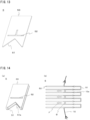
- FIG. 14 is a schematic configuration diagram showing an example of a grid of a circuit breaker according to Embodiment 6 of the present invention.
- FIG. 14(a) is a perspective view of the grid; and
- FIG. 14(b) is a side view in which a plurality of the grids are laminated.
- a grid 5 has a shape folded back in a U-shape in a length direction. As shown in FIG. 14 (a), the grid 5 folded back in the U-shape is provided with a notch portion 51 in a folded end portion and is provided with an insulating portion 52 that is made adjacent to a peak portion 51a of the notch portion 51. Furthermore, as shown in FIG.
- an arc 10 flowing through the grid 5 in a thickness direction forms an arc 10c that flows along the plate surface of the grid 5.
- the arc 10c traces a current path that flows from an arc discharge generation point of the arc 10 to the top portion 53 side via the folded end portion.
- the arc 10c forms magnetic flux ⁇ in a direction orthogonal with respect to the thickness direction of the grid 5.
- Electromagnetic force F which is driven by the magnetic flux ⁇ to the top portion 53 side in the opposite direction to both contact 1a, 2a sides, exerts on the arc 10 flowing in the thickness direction in the direction orthogonal with respect to the thickness direction of the grid 5.
- the grid 5 folded back in the U-shape is provided with the insulating portion 52 extended in the width direction, whereby electromagnetic repulsive force, which is directed toward both contact 1a, 2a sides and exerts on the arc 10 generated sandwiching the insulating portion 52, can be suppressed, and driving of the arc 10 in the opposite direction to both contact 1a, 2a sides can be expedited by the electromagnetic force F.
- FIG. 15 is a schematic configuration diagram showing a grid of a circuit breaker according to Embodiment 7 of the present invention.
- An insulating portion 52 of a grid 5 is formed in a V-shape along a notch portion 51.
- the grid 5 has a peak portion 52a of the insulating portion 52 adjacent to a peak portion 51a of the notch portion 51; and the insulating portion 52 has leg portions 521, 522 each extending from the peak portion 52a toward each side formed by the notch portion 51 and a top portion 53, the leg portions 521, 522 being coupled to form the V-shape.
- an arc 10c flowing along the plate surface of the grid 5 is generated by arcs 10a, 10b flowing through in a thickness direction.
- the arc 10c flows from the top portion 53 side to the notch portion 51 side and flows bypassing from the notch portion 51 side to the top portion 53 side along the V-shape of the insulating portion 52.
- Electromagnetic repulsive force Q exerts between the arc 10c directed toward the top portion 53 side from the notch portion 51 side of the grid 5 and the arc 10a on the notch portion 51 side sandwiching the insulating portion 52.
- the arc 10a on the notch portion 51 side is exerted by the electromagnetic repulsive force Q and is driven to the top portion 53 in the opposite direction to both contact 1a, 2a sides.
- the insulating portion 52 extended in the width direction of the grid 5 is provided, whereby the electromagnetic repulsive force, which is directed toward both contact 1a, 2a sides and exerts on the arc 10 generated sandwiching the insulating portion 5, can be suppressed;
- the insulating portion 52 is the V-shape, whereby the electromagnetic repulsive force Q directed toward the top portion 53 in the opposite direction to both contact 1a, 2a sides can exert on the arc 10a in which the arc 10 generates on the notch portion 51 side sandwiching the insulating portion 52; and therefore, breaking performance can be further improved.
- FIG. 16 is a schematic configuration diagram showing an example of a grid of a circuit breaker according to Embodiment 8 of the present invention.
- An insulating portion 52 of a grid 5 is formed of solid insulation material.
- the insulation material for example, thermosetting resin such as unsaturated polyester resin and melamine resin can be used.
- the insulating portion 52 may be formed of ceramics such as alumina and zirconia, as other material.
- insulating portion 52 of the grid 5 is formed of the insulation material, whereby electromagnetic repulsive force, which is directed toward both contact 1a, 2a sides and exerts on an arc 10 generated sandwiching the insulating portion 52, and the arc 10 can be prevented from passing through the insulating portion 52 and causing bridging.
- FIG. 17 is a top view showing the schematic configuration of a grid and a support plate of a circuit breaker according to Embodiment 9 of the present invention.
- the width W52 of an insulating portion 52 of a grid 5 is formed so as to be equal to or longer than the width W61 of an opening portion 61 of a support plate 6.
- the width W52 of the insulating portion 52 of the grid 5 is formed so as to be equal to or longer than the width W61 of the opening portion 61 of the support plate 6, whereby a current path, in which an arc 10c flowing along the plate surface of the grid 5 bypasses the insulating portion 52, is blocked. That is, the current path, which flows on the plate surface of the grid 5 from the top portion 53 side to the notch portion 51 side or from the notch portion 51 side to the top portion 53 side, is blocked and electromagnetic repulsive force, which is directed toward both contact 1a, 2a sides and exerts on an arc 10, is not generated. This suppresses the return of the arc 10 to both contact 1a, 2a sides from a state where the arc 10 is interrupted by the grids 5 and breaking performance can be improved.
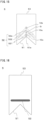
- FIG. 18 is a schematic configuration diagram of a circuit breaker according to Embodiment 10 of the present invention.
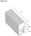
- FIG. 19 is a perspective view showing the schematic configuration of an arc chute of the circuit breaker according to Embodiment 10 of the present invention.
- the grids 5 are arranged in lamination from the lower side to the upper side of the arc chute 7; whereas, in this embodiment, grids 5 are arranged in parallel along the movable direction of a movable member 2.
- the grid 5 has a notch portion 51 formed on one end portion and an insulating portion 52 extended in a width direction.
- the notch portion 51 is arranged on both contact 1a, 2a sides of a fixed contact 1a and a movable contact 2a and a top portion 53 opposite to the notch portion 51 is arranged so as to face the upper side of the arc chute 7.
- a support plate 6 is provided on the plate surface of each grid 5 and an opening portion 61 is arranged so as to face both contact 1a, 2a sides.
- An exhaust port 16 which is for discharging arc gas 20 is provided on the upper side of the arc chute 7.
- This interrupts the arc 10 by the grids 5, can maintain a state where an arc voltage is elevated, and can improve breaking performance.
- the grid 5 is arranged so that the notch portion 51 faces the both contact 1a, 2a sides and the top portion 53 opposite to the notch portion 51 faces the upper side of the arc chute 7 provided with the exhaust port 16, whereby the arc gas 20 generated between both contact 1a, 2a can be efficiently sent to a gap 5d between the grids 5.
- the present invention may suitably combine a plurality of constituent elements disclosed in Embodiment 1 to 10 without departing from the spirit or scope of the present invention.
Landscapes
- Arc-Extinguishing Devices That Are Switches (AREA)
- Breakers (AREA)
Abstract
Description
- The present invention relates to a circuit breaker and a circuit breaking method, which include an arc chute arranged with grids.
- Hitherto, a circuit breaker that breaks current flowing through a circuit to protect an electric power apparatus from short circuit, ground short circuit, and the like has been used. In the circuit breaker, when contacts are separated off to break the current, an arc is generated between the contacts. When a fault current occurs, it is important to extinguish the generated arc immediately and to reduce breaking time for reducing damage of the electric power apparatus connected to the circuit. The circuit breaker generates an arc voltage higher than a power source voltage of the circuit and breaks the current by current limit by interrupting the arc by a plurality of grids arranged in an arc chute. In order to obtain high breaking performance, it is necessary to remain a state where the arc is interrupted by the grids and to maintain the elevated arc voltage.
Patent document 1 discloses a circuit breaker in which a notched portion is provided at an arc approach portion of a grid to generate electromagnetic force that draws the arc into the grid by the action of biasing magnetic flux. - Patent Document 1:
JP-A-2006-12540 - However, a problem exists in that when it becomes a state where the arc reaches the plate surface of the plate-shaped grid and flows through in a thickness direction, the electromagnetic force by the biasing magnetic flux is not generated and thus the arc interrupted by the grids continues again and breaking performance degrades.
- The present invention has been made to solve the aforementioned problem, and an object of the present invention is to provide a circuit breaker and a circuit breaking method, which improve breaking performance by suppressing the return of the arc to the contact sides and maintaining a high arc voltage.
- According to the present disclosure, a circuit breaker and a circuit breaking method as defined in the independent claims are provided. Further embodiments of the claimed invention are defined in the dependent claims. Although the claimed invention is only defined by the claims, the below embodiments, examples, and aspects are present for aiding in understanding the background and advantages of the claimed invention.
- A circuit breaker according to the present invention includes: a fixed member having a fixed contact; a movable member having a movable contact that is connected to and disconnected from the fixed contact; and an arc chute arranged with a plurality of laminated grids, each of which has a notch portion into which an arc generated between the fixed contact and the movable contact is drawn and an insulating portion which is adjacent to a peak portion of the notch portion and is extended in a width direction.
- A circuit breaking method according to the present invention is a circuit breaking method of a circuit breaker in which an arc generated between contact is interrupted by at least one grid to extinguish the arc, the circuit breaking method comprising the steps of: drawing the arc generated between the contact into a state where the arc generates arc discharge s at mutually different positions of the grid and flows through the grid; and bypassing currents flowing the grid between those generated arc discharges by an insulating portion provided between those mutually different positions of the grid to extinguish the arc.
- According to the circuit breaker of the present invention, the plurality of laminated grids, each of which has the insulating portion which is adjacent to the notch portion and is extended in the width direction, are arranged in the arc chute, whereby it becomes possible to suppress the return of the arc to the contact sides and to improve breaking performance. Furthermore, according to the circuit breaking method of the present invention, the currents flowing between the arcs in which arc discharges are generated at the mutually different positions of the grid are made to bypass by the insulating portion, whereby it becomes possible to suppress the return of the arc to the contact sides and to improve breaking performance.
-
-
FIG. 1 is a schematic configuration diagram showing a circuit breaker according toEmbodiment 1 of the present invention; -
FIG. 2 is a schematic configuration diagram showing an example of a grid of the circuit breaker according toEmbodiment 1 of the present invention; -
FIG. 3 is a schematic configuration diagram showing the grid and a support plate of the circuit breaker according toEmbodiment 1 of the present invention; -
FIG. 4 is a typical view showing an arc of the circuit breaker according toEmbodiment 1 of the present invention; -
FIG. 5 is a typical view showing the action of the arc of the circuit breaker according toEmbodiment 1 of the present invention; -
FIG. 6 is a typical view showing the action of the arc of the circuit breaker according toEmbodiment 1 of the present invention; -
FIG. 7 is a typical view for explaining the action of a grid of the circuit breaker according toEmbodiment 1 of the present invention; -
FIG. 8 is a typical view showing flows of arc gas of the circuit breaker according toEmbodiment 1 of the present invention; -
FIG. 9 is a schematic configuration diagram showing other example of the grid of the circuit breaker according toEmbodiment 1 of the present invention; -
FIG. 10 is a schematic configuration diagram showing an example of a grid of a circuit breaker according toEmbodiment 2 of the present invention; -
FIG. 11 is a schematic configuration diagram showing an example of a grid of a circuit breaker according toEmbodiment 3 of the present invention; -
FIG. 12 is a schematic configuration diagram showing an example of a grid of a circuit breaker according toEmbodiment 4 of the present invention; -
FIG. 13 is a schematic configuration diagram showing an example of a grid of a circuit breaker according toEmbodiment 5 of the present invention; -
FIG. 14 is a schematic configuration diagram showing an example of a grid of a circuit breaker according toEmbodiment 6 of the present invention; -
FIG. 15 is a schematic configuration diagram showing an example of a grid of a circuit breaker according toEmbodiment 7 of the present invention; -
FIG. 16 is a schematic configuration diagram showing an example of a grid of a circuit breaker according toEmbodiment 8 of the present invention; -
FIG. 17 is a schematic configuration diagram showing a grid and a support plate of a circuit breaker according to Embodiment 9 of the present invention; -
FIG. 18 is a schematic configuration diagram showing a circuit breaker according toEmbodiment 10 of the present invention; and -
FIG. 19 is a schematic configuration diagram showing an arc chute of the circuit breaker according toEmbodiment 10 of the present invention. -
FIG. 1 is a schematic configuration diagram showing a circuit breaker according toEmbodiment 1 of the present invention. As shown inFIG. 1 , acircuit breaker 100 includes: afixed member 1 having afixed contact 1a; amovable member 2 having amovable contact 2a; a fixed memberside arc horn 3 electrically connected to thefixed member 1; a movable memberside arc horn 4 electrically connected to themovable member 2; and anarc chute 7 arranged with a plurality ofgrids 5 that interrupt anarc 10 and a plurality ofsupport plates 6 that support thegrids 5. - The
circuit breaker 100 is arranged with anupper conductor 11 and alower conductor 12 below thearc chute 7. Theupper conductor 11 and thelower conductor 12 are electrically connected to thefixed member 1 and themovable member 2, respectively. Thefixed contact 1a is connected to and disconnected from themovable contact 2a, thereby energizing and breaking current between theupper conductor 11 and thelower conductor 12. - An
tripping device 13 connected to thelower conductor 12 detects overcurrent in breaking current and alatch 14 that holds themovable member 2 in energizing is released, whereby themovable member 2 is rotated in a direction away from the fixedmember 1 to open thefixed contact 1a and themovable contact 2a. Furthermore, when the opened state is brought to the energizing state shown inFIG. 1 , anactuator 15 coupled to themovable member 2 drives themovable member 2 to a position where themovable contact 2a comes in contact with the fixedcontact 1a. - The fixed member
side arc horn 3 is provided on an upper portion of the fixedmember 1; and the movable memberside arc horn 4 is provided on an upper portion of themovable member 2, the fixed memberside arc horn 3 and the movable memberside arc horn 4 being for guiding thearc 10 generated between thefixed contact 1a and themovable contact 2a (hereinafter, referred to as bothcontact arc chute 7. Each one end of the fixed memberside arc horn 3 and the movable memberside arc horn 4 is arranged adjacent to bothcontact - The
arc chute 7 has thegrid 5 formed of conductive plate-shaped metal and theinsulating support plate 6 that supports thegrid 5. The plurality of laminatedgrids 5 andsupport plates 6 are arranged with a predetermined distance on an upper portion of the fixed memberside arc horn 3 and the movable memberside arc horn 4. Thesupport plate 6 is arranged on the bottom surface of thegrid 5 to support thegrid 5 and to prevent thearc 10 from jumping out to bothcontact top surface plate 8 is arranged on the uppermost tier of thegrids 5. Thetop surface plate 8 preventsarc gas 20 generated by the heat of thearc 10 from leaking above thearc chute 7. An exhaust port 16 (not shown in the drawing) which is for discharging thearc gas 20 to the outside of thecircuit breaker 100 is provided on both sides of thearc chute 7. -
FIG. 2 is a schematic configuration diagram showing an example of the grid of the circuit breaker according toEmbodiment 1 of the present invention. As shown inFIG. 2 , thegrid 5 has anotch portion 51 formed on one end portion and aninsulating portion 52 which is adjacent to apeak portion 51a of thenotch portion 51 and is extended in a width direction. Here, a direction toward thenotch portion 51 and a direction toward atop portion 53 opposite to thenotch portion 51 are referred to as a length direction and a direction perpendicular to the length direction is referred to as a width direction. Theinsulating portion 52 is, for example, a slit-shaped through hole. Here,
the shape of thenotch portion 51 is a V-shape, a U-shape, a rectangular shape, or the like. -
FIG. 3 is a schematic configuration diagram showing the grid and the support plate of the circuit breaker according toEmbodiment 1 of the present invention. As shown inFIG. 3 , twogrids 5 are arranged on thesupport plate 6 so that thenotch portions 51 face to each other. Thesupport plate 6 is formed with an openingportion 61 in the center thereof and the insulatingportion 52 of thegrid 5 is arranged so as to overlap on the openingportion 61 of thesupport plate 6. Thesupport plate 6 is provided so that the center of the openingportion 61 is located at bothcontact FIG. 1 . That is, thegrids 5 are arranged so that thenotch portions 51 are directed toward bothcontacts - The
support plate 6 and thetop surface plate 8 are formed of thermosetting resin such as unsaturated polyester resin and melamine resin and may be formed of ceramics such as alumina and zirconia as other material. - Next, operation in breaking current of the
circuit breaker 100 according to the present invention will be described.FIG. 4 is a typical view showing an arc of the circuit breaker according toEmbodiment 1 of the present invention. - The
circuit breaker 100 is opened the contacts by separating themovable member 2 from the fixedmember 1 to generate thearc 10 between thefixed contact 1a and themovable contact 2a. The generatedarc 10 is commutated to the fixed memberside arc horn 3 or the movable memberside arc horn 4 arranged on the upper portion of bothcontact arc 10 is guided to thearc chute 7 by electromagnetic force that is exerted by magnetic flux produced by current flowing through the fixed memberside arc horn 3 or the movable member side arc horn 4 (hereinafter, referred to as botharc horns 3, 4). -
FIG. 5 is a typical view showing the action of the arc in the arc chute of the circuit breaker according toEmbodiment 1 of the present invention. FIG. 5(a) is a top view of the grid; and FIG. 5(b) is a perspective view of the grid. As shown inFIG. 5 , electromagnetic force F exerts on thearc 10 by biasing magnetic flux φ that passes through thegrid 5 and thearc 10 is drawn into thenotch portion 51 of thegrid 5 in thearc chute 7. Thearc 10 is driven toward thenotch portion 51 of thegrid 5 to come in contact with thegrid 5. Then, thearc 10 flows through in the thickness direction of thegrid 5 and is interrupted by the plurality ofgrids 5 arranged in lamination. -
FIG. 6 is a typical view showing the action of the arc in the grid of the circuit breaker according toEmbodiment 1 of the present invention. FIG. 6(a) is a perspective view of the grid; and FIG. 6(b) is a sectional view taken along the line A-A' of the grid. Thearc 10 flowing through in the thickness direction of thegrid 5 generates arc discharges at different positions of the plate surface of thegrid 5 due to differences of time from generation between bothcontacts grid 5, generation places of arc discharge on thegrid 5, and the like. As shown in FIG. 6(a), anarc 10a on thenotch portion 51 side and anarc 10b on thetop portion 53 side, thearc 10a and thearc 10b being generated sandwiching the insulatingportion 52 of thegrid 5, form anarc 10c that is current flowing along the plate surface of thegrid 5. Thearc 10c traces a current path that flows from thearc 10b on thetop portion 53 side to thearc 10a on thenotch portion 51 side, bypassing the insulatingportion 52. - Next, the action of the present invention will be described by comparing with a
grid 5 that has not an insulatingportion 52.FIG. 7 is a typical view for explaining the action of a grid according toEmbodiment 1 of the present invention. FIG. 7 (a) is a perspective view of the grid; and FIG. 7(b) is a sectional view taken along the line B-B' of the grid. As shown inFIG. 7 , in the case of thegrid 5 that has not the insulatingportion 52, electromagnetic repulsive force P exerts between thearc 10c flowing straight from thetop portion 53 side toward thenotch portion 51 side along the plate surface of thegrid 5 and thearcs grid 5. Thearc 10a on thenotch portion 51 side is drawn back to bothcontact - On the other hand, in the case of the
grid 5 having the insulatingportion 52 extended in the width direction according to the present invention shown inFIG. 6 , current flows bypassing the insulatingportion 52 without going straight in the length direction and therefore the electromagnetic repulsive force P that exerts on thearc 10a on thenotch portion 51 side can be suppressed. This can reduce current that flows straight in the length direction of thegrid 5 and can suppress the return of thearc 10a toward bothcontact -
FIG. 8 is a typical view showing a flow of arc gas according toEmbodiment 1 of the present invention. Thearc gas 20 generated at bothcontacts portion 61 of thesupport plate 6 to amutual gap 5d between thegrids 5 arranged in lamination and is discharged from theexhaust port 16 arranged on both sides of thearc chute 7 to the outside of thecircuit breaker 100. Furthermore, when the insulatingportion 52 of thegrid 5 is the through hole, thearc gas 20 generated at botharc horns grid 5 via the insulatingportion 52. Then, thearc gas 20 flows from the insulatingportion 52 to thegap 5d between thegrids 5 and is discharged from theexhaust port 16 to the outside of thecircuit breaker 100. Thearc 10 interrupted by thegrids 5 is driven to thetop portion 53 side in the opposite direction to bothcontact arc gas 20. - In such a manner, the insulating
portion 52 of thegrid 5 is the through hole, whereby in addition to thearc gas 20 generated between bothcontact arc gas 20 generated at botharc horns gap 5d between thegrids 5. This can drive thearc 10 to thetop portion 53 side in the opposite direction to bothcontact - As described above, the
circuit breaker 100 according to the present embodiment includes thearc chute 7 arranged with the plurality oflaminated grids 5, each of which has the insulatingportion 52 extended in the width direction, whereby the electromagnetic repulsive force, which is directed toward bothcontact arc 10 generated sandwiching the insulatingportion 52, can be suppressed. This interrupts thearc 10 by thegrids 5, can maintain a state where an arc voltage is elevated, and can improve breaking performance. Furthermore, the insulatingportion 52 is the through hole, whereby thearc gas 20 is efficiently sent to thegap 5d between thegrids 5, thearc 10 can be driven to thetop portion 53 side in the opposite direction to bothcontact - Incidentally, the shape and the position of the insulating
portion 52 of thegrid 5 can be suitably changed.FIG. 9 is other example of the grid of the circuit breaker according toEmbodiment 1 of the present invention. The width W52 of the insulatingportion 52 is preferable to be brought close to the width W5 of thegrid 5. This can lengthen distance in which current flowing along the plate surface of thegrid 5 bypasses the insulatingportion 52 without going straight in the length direction of thegrid 5. - Furthermore, the length of the side L52 of the insulating
portion 52 in the length direction of thegrid 5 is preferable to be lengthened in a range where thearc 10 flowing through in the thickness direction of thegrid 5 can be driven to thetop portion 53 side, sandwiching the insulatingportion 52. When the insulatingportion 52 of thegrid 5 is the through hole, the length of the side L52 of the insulatingportion 52 is lengthened and the area of the surface of thegrid 5 of the insulatingportion 52 is increased, whereby the inflow area of thearc gas 20 can be increased and driving in the opposite direction to bothcontact arc 10 can be expedited utilizing the gas flow. - Furthermore, the position of the insulating
portion 52 of thegrid 5 is preferable to be provided adjacent to thepeak portion 51a of thenotch portion 51. For example, the insulatingportion 52 is provided to thenotch portion 51 side than a midpoint of a line segment connecting thepeak portion 51a of thenotch portion 51 and thetop portion 53 opposite to thepeak portion 51a. This can further suppress the return of thearc 10 remained in the vicinity of thepeak portion 51a of thenotch portion 51. -
FIG. 10 is a schematic configuration diagram showing an example of a grid of a circuit breaker according toEmbodiment 2 of the present invention. Two insulatingportions 52 of agrid 5 are formed with a predetermined distance spaced in a length direction. The number of insulatingportions 52 of thegrid 5 may be further increased to three or four. The number of the insulatingportions 52 is increased, whereby electromagnetic repulsive force, which is directed toward bothcontact arc 10 generated sandwiching the insulatingportion 52, can be suppressed; and when the insulatingportion 52 is a through hole, the inflow area ofarc gas 20 can be increased and driving in the opposite direction to bothcontact arc 10 can be expedited utilizing a gas flow. -
FIG. 11 is a schematic configuration diagram showing an example of a grid of a circuit breaker according toEmbodiment 3 of the present invention. An insulatingportion 52 of agrid 5 is formed so as to be connected with anotch portion 51. The insulatingportion 52 is a through hole and aslit 51b is provided between thenotch portion 51 and the insulatingportion 52, whereby thenotch portion 51 and the insulatingportion 52 can be communicated with each other. This can suppress electromagnetic repulsive force, which is directed toward bothcontact arc 10 generated sandwiching the insulatingportion 52, and processing of the insulatingportion 52 of thegrid 5 becomes easy. -
FIG. 12 is a schematic configuration diagram showing an example of a grid of a circuit breaker according toEmbodiment 4 of the present invention. Agrid 5 is segmented in a length direction to be electrically connected. For example, thegrid 5 is segmented into a dividedgrid 5a on thetop portion 53 side and a dividedgrid 5b on thenotch portion 51 side; and the dividedgrids connection portions 5c. Theconnection portion 5c is, for example, a electric wire, a connecting pin, a rivet, or the like. Furthermore, the dividedgrids grid 5a and the dividedgrid 5b functions as an insulatingportion 52; and similarly, electromagnetic repulsive force, which is directed toward bothcontact arc 10, can be suppressed. Further, the width W52 and the length L52 of the insulatingportion 52 can be suitably adjusted and therefore the distance between the dividedgrids -
FIG. 13 is a schematic configuration diagram showing an example of a grid of a circuit breaker according toEmbodiment 5 of the present invention. An insulatingportion 52 of agrid 5 is formed in a T-shape. The insulatingportion 52 is formed by a portion extended in a width direction and a portion extended from the center position thereof toward atop portion 53. The insulatingportion 52 is formed in the T-shape, whereby a distance in which current flowing along the plate surface of thegrid 5 bypasses the insulatingportion 52 without going straight in a length direction can be lengthened and electromagnetic repulsive force directed toward bothcontact -
FIG. 14 is a schematic configuration diagram showing an example of a grid of a circuit breaker according toEmbodiment 6 of the present invention. FIG. 14(a) is a perspective view of the grid; and FIG. 14(b) is a side view in which a plurality of the grids are laminated. Agrid 5 has a shape folded back in a U-shape in a length direction. As shown in FIG. 14 (a), thegrid 5 folded back in the U-shape is provided with anotch portion 51 in a folded end portion and is provided with an insulatingportion 52 that is made adjacent to apeak portion 51a of thenotch portion 51. Furthermore, as shown in FIG. 14(b), anarc 10 flowing through thegrid 5 in a thickness direction forms anarc 10c that flows along the plate surface of thegrid 5. Thearc 10c traces a current path that flows from an arc discharge generation point of thearc 10 to thetop portion 53 side via the folded end portion. Thearc 10c forms magnetic flux Φ in a direction orthogonal with respect to the thickness direction of thegrid 5. Electromagnetic force F, which is driven by the magnetic flux Φ to thetop portion 53 side in the opposite direction to bothcontact arc 10 flowing in the thickness direction in the direction orthogonal with respect to the thickness direction of thegrid 5. - As described above, in the present embodiment, the
grid 5 folded back in the U-shape is provided with the insulatingportion 52 extended in the width direction, whereby electromagnetic repulsive force, which is directed toward bothcontact arc 10 generated sandwiching the insulatingportion 52, can be suppressed, and driving of thearc 10 in the opposite direction to bothcontact -
FIG. 15 is a schematic configuration diagram showing a grid of a circuit breaker according toEmbodiment 7 of the present invention. An insulatingportion 52 of agrid 5 is formed in a V-shape along anotch portion 51. Thegrid 5 has apeak portion 52a of the insulatingportion 52 adjacent to apeak portion 51a of thenotch portion 51; and the insulatingportion 52 hasleg portions peak portion 52a toward each side formed by thenotch portion 51 and atop portion 53, theleg portions grid 5, anarc 10c flowing along the plate surface of thegrid 5 is generated byarcs arc 10c flows from thetop portion 53 side to thenotch portion 51 side and flows bypassing from thenotch portion 51 side to thetop portion 53 side along the V-shape of the insulatingportion 52. Electromagnetic repulsive force Q exerts between thearc 10c directed toward thetop portion 53 side from thenotch portion 51 side of thegrid 5 and thearc 10a on thenotch portion 51 side sandwiching the insulatingportion 52. Thearc 10a on thenotch portion 51 side is exerted by the electromagnetic repulsive force Q and is driven to thetop portion 53 in the opposite direction to bothcontact - As described above, in the present embodiment, the insulating
portion 52 extended in the width direction of thegrid 5 is provided, whereby the electromagnetic repulsive force, which is directed toward bothcontact arc 10 generated sandwiching the insulatingportion 5, can be suppressed; the insulatingportion 52 is the V-shape, whereby the electromagnetic repulsive force Q directed toward thetop portion 53 in the opposite direction to bothcontact arc 10a in which thearc 10 generates on thenotch portion 51 side sandwiching the insulatingportion 52; and therefore, breaking performance can be further improved. -
FIG. 16 is a schematic configuration diagram showing an example of a grid of a circuit breaker according toEmbodiment 8 of the present invention. An insulatingportion 52 of agrid 5 is formed of solid insulation material. As the insulation material, for example, thermosetting resin such as unsaturated polyester resin and melamine resin can be used. The insulatingportion 52 may be formed of ceramics such as alumina and zirconia, as other material. Then insulatingportion 52 of thegrid 5 is formed of the insulation material, whereby electromagnetic repulsive force, which is directed toward bothcontact arc 10 generated sandwiching the insulatingportion 52, and thearc 10 can be prevented from passing through the insulatingportion 52 and causing bridging. -
FIG. 17 is a top view showing the schematic configuration of a grid and a support plate of a circuit breaker according to Embodiment 9 of the present invention. In acircuit breaker 100 according to the present embodiment, the width W52 of an insulatingportion 52 of agrid 5 is formed so as to be equal to or longer than the width W61 of anopening portion 61 of asupport plate 6. - The width W52 of the insulating
portion 52 of thegrid 5 is formed so as to be equal to or longer than the width W61 of the openingportion 61 of thesupport plate 6, whereby a current path, in which anarc 10c flowing along the plate surface of thegrid 5 bypasses the insulatingportion 52, is blocked. That is, the current path, which flows on the plate surface of thegrid 5 from thetop portion 53 side to thenotch portion 51 side or from thenotch portion 51 side to thetop portion 53 side, is blocked and electromagnetic repulsive force, which is directed toward bothcontact arc 10, is not generated. This suppresses the return of thearc 10 to bothcontact arc 10 is interrupted by thegrids 5 and breaking performance can be improved. -
FIG. 18 is a schematic configuration diagram of a circuit breaker according toEmbodiment 10 of the present invention.FIG. 19 is a perspective view showing the schematic configuration of an arc chute of the circuit breaker according toEmbodiment 10 of the present invention. InEmbodiment 1, thegrids 5 are arranged in lamination from the lower side to the upper side of thearc chute 7; whereas, in this embodiment,grids 5 are arranged in parallel along the movable direction of amovable member 2. - The
grid 5 has anotch portion 51 formed on one end portion and an insulatingportion 52 extended in a width direction. In thegrid 5, thenotch portion 51 is arranged on bothcontact fixed contact 1a and amovable contact 2a and atop portion 53 opposite to thenotch portion 51 is arranged so as to face the upper side of thearc chute 7. Asupport plate 6 is provided on the plate surface of eachgrid 5 and anopening portion 61 is arranged so as to face bothcontact exhaust port 16 which is for dischargingarc gas 20 is provided on the upper side of thearc chute 7. - In such a manner, the
arc chute 7, in which thegrids 5 each having the insulatingportion 52 extended in the width direction are arranged in parallel along the movable direction of themovable member 2, is provided, whereby electromagnetic repulsive force, which is directed toward bothcontact arc 10 generated sandwiching the insulatingportion 52, can be suppressed. This interrupts thearc 10 by thegrids 5, can maintain a state where an arc voltage is elevated, and can improve breaking performance. Furthermore, thegrid 5 is arranged so that thenotch portion 51 faces the bothcontact top portion 53 opposite to thenotch portion 51 faces the upper side of thearc chute 7 provided with theexhaust port 16, whereby thearc gas 20 generated between bothcontact gap 5d between thegrids 5. - Incidentally, the present invention may suitably combine a plurality of constituent elements disclosed in
Embodiment 1 to 10 without departing from the spirit or scope of the present invention. - Further, the present disclosure includes configurations as defined by the following clauses:
- (1) A circuit breaker comprising:
- a fixed member having a fixed contact;
- a movable member having a movable contact that is connected to and disconnected from the fixed contact; and
- an arc chute arranged with a plurality of laminated grids, each of which has a notch portion into which an arc generated between the fixed contact and the movable contact is drawn and an insulating portion which is adjacent to a peak portion of the notch portion and is extended in a width direction.
- (2) The circuit breaker according to clause (1), wherein
the insulating portion of the grid is provided so that current directed toward the top portion side opposite to the notch portion from the notch portion side and current directed toward the notch portion side from the top portion side are made to bypass in the width direction of the grid. - (3) The circuit breaker according to clause (1) or (2), wherein the insulating portion is a through hole provided in the grid.
- (4) The circuit breaker according to claim (3), wherein
the notch portion and the insulating portion of the grid are communicated with each other. - (5) The circuit breaker according to clause (1) or (2), wherein the insulating portion is formed of solid insulation material.
- (6) The circuit breaker according to clause (1) or (2), wherein
- the grid is segmented into the notch portion side and the top portion side to be mutually electrically connected with a distance spaced therebetween; and
- the distance is the insulating portion.
- (7) The circuit breaker according to clause (1) or (2), wherein
- the grid is folded back in a U-shape in a length direction; and
- the folded end portion is provided with the notch portion.
- (8) The circuit breaker according to any one of clause (1) to (5), wherein
the insulating portion has leg portions each extending in a width direction, the leg portions being coupled to form a V-shape. - (9) The circuit breaker according to any one of clause (1) to (8), wherein
- the grid is supported by a support plate having an opening portion in the center thereof; and
- the insulating portion of the grid is arranged so as to overlap with the opening portion of the support plate.
- (10) The circuit breaker according to clause (9), wherein
the width of the insulating portion of the grid is equal to or larger than the width of the opening portion of the support plate. - (11) A circuit breaker in which an arc generated between contact is interrupted by at least one grid to extinguish the arc, wherein the grid has an insulating portion;
- the arc generated between the contact is drawn into the grid, generates arc discharges at mutually different positions of the grid, and flows through the grid; and
- the insulating portion is provided between those mutually different positions of the grid and makes current flowing through the grid between those generated arc discharges bypass.
- (12) A circuit breaker comprising:
- a first and a second contact; and
- an arc chute arranged with a grid which has a notch portion into which an arc generated between the first and the second contact is drawn and a through hole, wherein
- arc gas flows passing through the through hole in the thickness direction of the grid.
- 13. A circuit breaking method of a circuit breaker in which an arc generated between contact is interrupted by at least one grid to extinguish the arc, the circuit breaking method comprising the steps of:
- drawing the arc generated between the contact into a state where the arc generates arc discharges at mutually different positions of the grid and flows through the grid; and
- bypassing currents flowing the grid between those generated arc discharges by an insulating portion provided between those mutually different positions of the grid to extinguish the arc.
-
- 1
- Fixed member
- 2
- Movable member
- 3
- Fixed member side arc horn
- 4
- Movable member side arc horn
- 5
- Grid
- 51
- Notch portion
- 52
- Insulating portion
- 6
- Support plate
- 61
- Opening portion
- 7
- Arc chute
- 8
- Top surface plate
- 10
- Arc
- 11
- Upper conductor
- 12
- Lower conductor
- 13
- Tripping device
- 14
- Latch
- 15
- Actuator
- 16
- Exhaust port
- 100
- Circuit breaker
Claims (8)
- A circuit breaker in which an arc generated between contact (1a, 2a) is interrupted by at least one grid (5) to extinguish the arc (10), whereinthe grid (5) has an insulating portion (52);the arc (10) generated between the contact (1a, 2a) is drawn into the grid (5), generates arc discharges at mutually different positions of the grid (5), and flows through the grid (5); andthe insulating portion (52) is provided between those mutually different positions of the grid (5) and makes current flowing through the grid (5) between those generated arc discharges bypass.
- The circuit breaker according to claim 1, wherein
the insulating portion (52) is a through hole provided in the grid (5). - The circuit breaker according to claim 1 or 2, wherein
the insulating portion (52) is formed of solid insulation material. - The circuit breaker according to any one of claim 1 to 3, wherein
the insulating portion (52) has leg portions each extending in a width direction, the leg portions being coupled to form a V-shape. - The circuit breaker according to any one of claim 1 to 4, whereinthe grid (5) is supported by a support plate (6) having an opening portion (61) in the center thereof; andthe insulating portion (52) of the grid (5) is arranged so as to overlap with the opening portion (61) of the support plate (6) .
- The circuit breaker according to claim 5, wherein
the width of the insulating portion (52) of the grid (5) is equal to or larger than the width of the opening portion (61) of the support plate (6). - The circuit breaker according to claim 2, wherein
arc gas flows passing through the through hole in the thickness direction of the grid (5). - A circuit breaking method of a circuit breaker in which an arc (10) generated between contact (1a, 2a) is interrupted by at least one grid (5) to extinguish the arc (10), the circuit breaking method comprising the steps of:drawing the arc (10) generated between the contact (1a, 2a) into a state where the arc (10) generates arc discharges at mutually different positions of the grid (5) and flows through the grid (5) ; andbypassing currents flowing the grid (5) between those generated arc discharges by an insulating portion (52) provided between those mutually different positions of the grid (5) to extinguish the arc (10).
Applications Claiming Priority (3)
| Application Number | Priority Date | Filing Date | Title |
|---|---|---|---|
| JP2018016138 | 2018-02-01 | ||
| PCT/JP2018/029414 WO2019150613A1 (en) | 2018-02-01 | 2018-08-06 | Circuit breaker and circuit breaking method |
| EP18904243.5A EP3748666B1 (en) | 2018-02-01 | 2018-08-06 | Circuit breaker and circuit breaking method |
Related Parent Applications (2)
| Application Number | Title | Priority Date | Filing Date |
|---|---|---|---|
| EP18904243.5A Division-Into EP3748666B1 (en) | 2018-02-01 | 2018-08-06 | Circuit breaker and circuit breaking method |
| EP18904243.5A Division EP3748666B1 (en) | 2018-02-01 | 2018-08-06 | Circuit breaker and circuit breaking method |
Publications (2)
| Publication Number | Publication Date |
|---|---|
| EP4258314A2 true EP4258314A2 (en) | 2023-10-11 |
| EP4258314A3 EP4258314A3 (en) | 2024-01-17 |
Family
ID=67479628
Family Applications (2)
| Application Number | Title | Priority Date | Filing Date |
|---|---|---|---|
| EP18904243.5A Active EP3748666B1 (en) | 2018-02-01 | 2018-08-06 | Circuit breaker and circuit breaking method |
| EP23195006.4A Pending EP4258314A3 (en) | 2018-02-01 | 2018-08-06 | Circuit breaker and circuit breaking method |
Family Applications Before (1)
| Application Number | Title | Priority Date | Filing Date |
|---|---|---|---|
| EP18904243.5A Active EP3748666B1 (en) | 2018-02-01 | 2018-08-06 | Circuit breaker and circuit breaking method |
Country Status (3)
| Country | Link |
|---|---|
| EP (2) | EP3748666B1 (en) |
| JP (1) | JP6516078B1 (en) |
| WO (1) | WO2019150613A1 (en) |
Families Citing this family (8)
| Publication number | Priority date | Publication date | Assignee | Title |
|---|---|---|---|---|
| EP4187572B1 (en) * | 2019-05-28 | 2025-09-24 | Mitsubishi Electric Corporation | Direct-current circuit breaker |
| KR102788742B1 (en) * | 2020-03-10 | 2025-03-31 | 엘에스일렉트릭(주) | Direct Current Circuit Breaker |
| EP3933866B1 (en) * | 2020-07-01 | 2026-01-28 | ABB Schweiz AG | A switching apparatus for electric power distribution grids |
| KR102754542B1 (en) * | 2021-02-26 | 2025-01-14 | 엘에스일렉트릭(주) | Arc chute and Load break switch including the same |
| KR102754543B1 (en) * | 2021-02-26 | 2025-01-14 | 엘에스일렉트릭(주) | Arc chute and Load break switch including the same |
| KR102804378B1 (en) * | 2022-05-17 | 2025-05-09 | 에이치디현대일렉트릭 주식회사 | Circuit breaker |
| KR102696708B1 (en) * | 2022-05-24 | 2024-08-21 | 에이치디현대일렉트릭 주식회사 | Circuit breaker |
| CN116190176B (en) * | 2023-04-07 | 2024-07-09 | 南京双京电器集团有限公司 | Low-voltage circuit breaker |
Citations (1)
| Publication number | Priority date | Publication date | Assignee | Title |
|---|---|---|---|---|
| JP2006012540A (en) | 2004-06-24 | 2006-01-12 | Hitachi Ltd | Circuit breaker |
Family Cites Families (10)
| Publication number | Priority date | Publication date | Assignee | Title |
|---|---|---|---|---|
| NL86694C (en) * | 1951-05-03 | |||
| CH594976A5 (en) * | 1976-05-07 | 1978-01-31 | Bbc Brown Boveri & Cie | |
| JPS5489278A (en) * | 1977-12-27 | 1979-07-16 | Mitsubishi Electric Corp | Arc extinguishing apparatus |
| JPS59113946U (en) * | 1983-01-20 | 1984-08-01 | 三菱電機株式会社 | switch |
| KR910001537B1 (en) * | 1987-04-21 | 1991-03-15 | 미쓰비시전기 주식회사 | Circuit breaker |
| CH681933A5 (en) * | 1991-03-14 | 1993-06-15 | Secheron Sa | Electrical switch with arc-quenching system - has plate of magnetic material with coupled plate of insulation having cut-away section near to arcing point |
| JP3896322B2 (en) * | 2002-10-31 | 2007-03-22 | エナジーサポート株式会社 | Arc extinguishing device |
| JP2015032376A (en) * | 2013-07-31 | 2015-02-16 | 富士電機機器制御株式会社 | Circuit breaker |
| US9153399B2 (en) * | 2013-11-15 | 2015-10-06 | Eaton Corporation | ARC baffling device |
| CN107068456B (en) * | 2017-07-01 | 2018-04-24 | 龚柱 | Arc extinguishing grid pieces and the arc-control device comprising the arc extinguishing grid pieces and the switch comprising the arc-control device |
-
2018
- 2018-08-06 WO PCT/JP2018/029414 patent/WO2019150613A1/en not_active Ceased
- 2018-08-06 EP EP18904243.5A patent/EP3748666B1/en active Active
- 2018-08-06 JP JP2018567764A patent/JP6516078B1/en active Active
- 2018-08-06 EP EP23195006.4A patent/EP4258314A3/en active Pending
Patent Citations (1)
| Publication number | Priority date | Publication date | Assignee | Title |
|---|---|---|---|---|
| JP2006012540A (en) | 2004-06-24 | 2006-01-12 | Hitachi Ltd | Circuit breaker |
Also Published As
| Publication number | Publication date |
|---|---|
| EP3748666B1 (en) | 2023-10-11 |
| EP4258314A3 (en) | 2024-01-17 |
| EP3748666A4 (en) | 2021-06-30 |
| EP3748666A1 (en) | 2020-12-09 |
| JP6516078B1 (en) | 2019-05-22 |
| WO2019150613A1 (en) | 2019-08-08 |
| JPWO2019150613A1 (en) | 2020-02-06 |
Similar Documents
| Publication | Publication Date | Title |
|---|---|---|
| EP3748666B1 (en) | Circuit breaker and circuit breaking method | |
| EP3149755B1 (en) | Electrical switching apparatus, and arc chute assembly and barrier member therefor | |
| EP2561534B1 (en) | Circuit interrupter with enhanced arc quenching capabilities | |
| EP1388154B1 (en) | Electrical switching apparatus having an arc runner with an elongated raised ridge | |
| KR200460487Y1 (en) | Circuit breaker with an arc extinguishing device | |
| CN101625934B (en) | Circuit breaker | |
| JP2010251299A (en) | Circuit breaker | |
| CN101243529B (en) | Electromechanical circuit breaker and method of breaking the current in said electromechanical circuit breaker | |
| HK40096535A (en) | Circuit breaker and circuit breaking method | |
| HK40035091A (en) | Circuit breaker and circuit breaking method | |
| HK40035091B (en) | Circuit breaker and circuit breaking method | |
| CN102237230B (en) | Double interrupted protective switching device for monitoring circuit | |
| CN100356493C (en) | Electric switcher | |
| JP6966002B2 (en) | Circuit breaker | |
| KR20210133637A (en) | Grid to remove arc and assembly having the same | |
| JP3647536B2 (en) | Switch | |
| CN221176018U (en) | Arc extinguishing assembly and contactor | |
| CN103117197B (en) | For the arc-chutes device of electromagentic switching apparatus | |
| JP7580990B2 (en) | Circuit Breakers | |
| JP7330385B2 (en) | DC circuit breaker | |
| CN121399713A (en) | Switchgear panel | |
| KR20250006533A (en) | Grid, arc extinguishing unit and circuit breaker | |
| CN116844894A (en) | Arc extinguishing system of electric switch and electric switch | |
| CN117393349A (en) | Arc extinguishing components and contactors | |
| CN116844892A (en) | Electrical equipment switch |
Legal Events
| Date | Code | Title | Description |
|---|---|---|---|
| PUAI | Public reference made under article 153(3) epc to a published international application that has entered the european phase |
Free format text: ORIGINAL CODE: 0009012 |
|
| STAA | Information on the status of an ep patent application or granted ep patent |
Free format text: STATUS: REQUEST FOR EXAMINATION WAS MADE |
|
| 17P | Request for examination filed |
Effective date: 20230904 |
|
| AC | Divisional application: reference to earlier application |
Ref document number: 3748666 Country of ref document: EP Kind code of ref document: P |
|
| AK | Designated contracting states |
Kind code of ref document: A2 Designated state(s): AL AT BE BG CH CY CZ DE DK EE ES FI FR GB GR HR HU IE IS IT LI LT LU LV MC MK MT NL NO PL PT RO RS SE SI SK SM TR |
|
| REG | Reference to a national code |
Ref country code: DE Ref legal event code: R079 Free format text: PREVIOUS MAIN CLASS: H01H0033100000 Ipc: H01H0073180000 |
|
| PUAL | Search report despatched |
Free format text: ORIGINAL CODE: 0009013 |
|
| AK | Designated contracting states |
Kind code of ref document: A3 Designated state(s): AL AT BE BG CH CY CZ DE DK EE ES FI FR GB GR HR HU IE IS IT LI LT LU LV MC MK MT NL NO PL PT RO RS SE SI SK SM TR |
|
| RIC1 | Information provided on ipc code assigned before grant |
Ipc: H01H 33/10 20060101ALI20231208BHEP Ipc: H01H 9/36 20060101ALI20231208BHEP Ipc: H01H 73/18 20060101AFI20231208BHEP |
|
| REG | Reference to a national code |
Ref country code: HK Ref legal event code: DE Ref document number: 40096535 Country of ref document: HK |
|
| STAA | Information on the status of an ep patent application or granted ep patent |
Free format text: STATUS: EXAMINATION IS IN PROGRESS |
|
| 17Q | First examination report despatched |
Effective date: 20251010 |