EP4255160A1 - Piezoelectric-body film joint substrate and manufacturing method thereof - Google Patents
Piezoelectric-body film joint substrate and manufacturing method thereof Download PDFInfo
- Publication number
- EP4255160A1 EP4255160A1 EP23160680.7A EP23160680A EP4255160A1 EP 4255160 A1 EP4255160 A1 EP 4255160A1 EP 23160680 A EP23160680 A EP 23160680A EP 4255160 A1 EP4255160 A1 EP 4255160A1
- Authority
- EP
- European Patent Office
- Prior art keywords
- film
- piezoelectric
- substrate
- body film
- aln
- Prior art date
- Legal status (The legal status is an assumption and is not a legal conclusion. Google has not performed a legal analysis and makes no representation as to the accuracy of the status listed.)
- Granted
Links
Images




Classifications
-
- H—ELECTRICITY
- H10—SEMICONDUCTOR DEVICES; ELECTRIC SOLID-STATE DEVICES NOT OTHERWISE PROVIDED FOR
- H10N—ELECTRIC SOLID-STATE DEVICES NOT OTHERWISE PROVIDED FOR
- H10N30/00—Piezoelectric or electrostrictive devices
- H10N30/01—Manufacture or treatment
- H10N30/07—Forming of piezoelectric or electrostrictive parts or bodies on an electrical element or another base
- H10N30/072—Forming of piezoelectric or electrostrictive parts or bodies on an electrical element or another base by laminating or bonding of piezoelectric or electrostrictive bodies
- H10N30/073—Forming of piezoelectric or electrostrictive parts or bodies on an electrical element or another base by laminating or bonding of piezoelectric or electrostrictive bodies by fusion of metals or by adhesives
-
- H—ELECTRICITY
- H10—SEMICONDUCTOR DEVICES; ELECTRIC SOLID-STATE DEVICES NOT OTHERWISE PROVIDED FOR
- H10N—ELECTRIC SOLID-STATE DEVICES NOT OTHERWISE PROVIDED FOR
- H10N30/00—Piezoelectric or electrostrictive devices
- H10N30/01—Manufacture or treatment
- H10N30/05—Manufacture of multilayered piezoelectric or electrostrictive devices, or parts thereof, e.g. by stacking piezoelectric bodies and electrodes
- H10N30/057—Manufacture of multilayered piezoelectric or electrostrictive devices, or parts thereof, e.g. by stacking piezoelectric bodies and electrodes by stacking bulk piezoelectric or electrostrictive bodies and electrodes
-
- H—ELECTRICITY
- H10—SEMICONDUCTOR DEVICES; ELECTRIC SOLID-STATE DEVICES NOT OTHERWISE PROVIDED FOR
- H10N—ELECTRIC SOLID-STATE DEVICES NOT OTHERWISE PROVIDED FOR
- H10N30/00—Piezoelectric or electrostrictive devices
- H10N30/01—Manufacture or treatment
- H10N30/06—Forming electrodes or interconnections, e.g. leads or terminals
-
- H—ELECTRICITY
- H10—SEMICONDUCTOR DEVICES; ELECTRIC SOLID-STATE DEVICES NOT OTHERWISE PROVIDED FOR
- H10N—ELECTRIC SOLID-STATE DEVICES NOT OTHERWISE PROVIDED FOR
- H10N30/00—Piezoelectric or electrostrictive devices
- H10N30/101—Piezoelectric or electrostrictive devices with electrical and mechanical input and output, e.g. having combined actuator and sensor parts
-
- H—ELECTRICITY
- H10—SEMICONDUCTOR DEVICES; ELECTRIC SOLID-STATE DEVICES NOT OTHERWISE PROVIDED FOR
- H10N—ELECTRIC SOLID-STATE DEVICES NOT OTHERWISE PROVIDED FOR
- H10N30/00—Piezoelectric or electrostrictive devices
- H10N30/50—Piezoelectric or electrostrictive devices having a stacked or multilayer structure
-
- H—ELECTRICITY
- H10—SEMICONDUCTOR DEVICES; ELECTRIC SOLID-STATE DEVICES NOT OTHERWISE PROVIDED FOR
- H10N—ELECTRIC SOLID-STATE DEVICES NOT OTHERWISE PROVIDED FOR
- H10N30/00—Piezoelectric or electrostrictive devices
- H10N30/50—Piezoelectric or electrostrictive devices having a stacked or multilayer structure
- H10N30/503—Piezoelectric or electrostrictive devices having a stacked or multilayer structure having a non-rectangular cross-section in a plane orthogonal to the stacking direction, e.g. polygonal or circular in top view
-
- H—ELECTRICITY
- H10—SEMICONDUCTOR DEVICES; ELECTRIC SOLID-STATE DEVICES NOT OTHERWISE PROVIDED FOR
- H10N—ELECTRIC SOLID-STATE DEVICES NOT OTHERWISE PROVIDED FOR
- H10N30/00—Piezoelectric or electrostrictive devices
- H10N30/704—Piezoelectric or electrostrictive devices based on piezoelectric or electrostrictive films or coatings
- H10N30/706—Piezoelectric or electrostrictive devices based on piezoelectric or electrostrictive films or coatings characterised by the underlying bases, e.g. substrates
- H10N30/708—Intermediate layers, e.g. barrier, adhesion or growth control buffer layers
Definitions
- the present disclosure relates to a piezoelectric-body film joint substrate and a manufacturing method thereof.
- Patent Reference 1 Japanese Patent Application Publication No. 2018-190890 (Patent Reference 1), for example.
- a high-performance device including a plurality of piezoelectric films cannot be obtained when a plurality of piezoelectric films of different types are stacked on the same substrate in a conventional device.
- An object of the present disclosure is to provide a high-performance piezoelectric-body film joint substrate in which piezoelectric films of two or more types are provided in superimposition with each other on the same substrate and a manufacturing method thereof.
- a piezoelectric-body film joint substrate in the present disclosure includes a substrate, a substrate electrode provided on the substrate, a first piezoelectric-body film stuck on the substrate electrode and including a first piezoelectric film and a first upper electrode film formed on the first piezoelectric film, and a second piezoelectric-body film stuck on the first upper electrode film and including a second piezoelectric film different from the first piezoelectric film and a second upper electrode film formed on the second piezoelectric film.
- a method of manufacturing a piezoelectric-body film joint substrate in the present disclosure includes peeling off a first piezoelectric-body film formed on a first substrate and including a first piezoelectric film and a first electrode film provided on the first piezoelectric film and a second piezoelectric-body film formed on a second substrate and including a second piezoelectric film and a second electrode film provided on the second piezoelectric film respectively from the first substrate and the second substrate, sticking the first piezoelectric-body film on an electrode formed on a third substrate different from both of the first substrate and the second substrate, and sticking the second piezoelectric-body film on the first piezoelectric-body film.
- the piezoelectric-body film joint substrate is a product as an intermediate in which a plurality of piezoelectric films are provided on the same substrate. While the piezoelectric films are desired to be monocrystalline piezoelectric films, it is also possible to form the piezoelectric-body film joint substrate with polycrystalline piezoelectric films.
- a piezoelectric film integrated device including a plurality of piezoelectric bodies can be manufactured.
- the piezoelectric film integrated device is an acoustic oscillation sensor, for example.
- the acoustic oscillation sensor is a sensor that detects status (e.g., distance, shape, movement or the like) of a detection target object by outputting an acoustic oscillatory wave and detecting reflected waves of the acoustic oscillatory wave.
- the acoustic oscillation sensor is referred to also as an "ultrasonic sensor".
- the acoustic oscillatory wave is made up of at least one of a sonic wave and an ultrasonic wave.
- the acoustic oscillatory wave includes a sonic wave, an ultrasonic wave, or both of a sonic wave and an ultrasonic wave.
- Fig. 1 is a side view schematically showing the structure of a piezoelectric-body film joint substrate 100 according to a first embodiment.
- Fig. 2 is a top view schematically showing the structure of the piezoelectric-body film joint substrate 100.
- Fig. 3 is a cross-sectional view of the piezoelectric-body film joint substrate 100 in Fig. 2 taken along the line S3-S3.
- the piezoelectric-body film joint substrate 100 includes an SOI substrate 33 as a substrate and a platinum (Pt) film 34 as an electrode (i.e., substrate electrode) provided on the SOI substrate 33. As shown in Fig. 2 , the Pt film 34 is connected to a wiring layer formed on the SOI substrate 33.
- the SOI stands for Silicon On Insulator.
- a drive circuit for driving the piezoelectric-body film joint substrate 100 and thereby generating the acoustic oscillatory wave a processing circuit that executes a process by using an acoustic oscillatory wave detection signal, and so forth.
- the piezoelectric-body film joint substrate 100 includes an AlN piezoelectric-body film 27 as a first piezoelectric-body film stuck (i.e., bonded) on the Pt film 34 being the substrate electrode and a PZT piezoelectric-body film 17 as a second piezoelectric-body film stuck (i.e., bonded) on the AlN piezoelectric-body film 27.
- the AlN piezoelectric-body film 27 includes an AlN film 25 as a first piezoelectric film and a Pt film 26 as a first upper electrode film formed on the AlN film 25.
- the PZT piezoelectric-body film 17 includes a PZT film 15 as a second piezoelectric film different from the first piezoelectric film (e.g., in crystal structure) and a Pt film 16 as a second upper electrode film formed on the PZT film 15, and is stuck on the Pt film 26. Further, area of the PZT piezoelectric-body film 17 and area of the AlN piezoelectric-body film 27 differ from each other. In the first embodiment, the area of the PZT piezoelectric-body film 17 is smaller than the area of the AlN piezoelectric-body film 27.
- the AlN represents aluminum nitride.
- the PZT represents piezoelectric zirconate titanate (lead zirconate titanate).
- a different piezoelectric film such as a lithium tantalate (LiTaO 3 ) piezoelectric-body film or a lithium niobate (LiNbO 3 ) piezoelectric-body film may be used.
- the second piezoelectric-body film instead of the PZT piezoelectric-body film, a different piezoelectric-body film such as a potassium sodium niobate (KNN) piezoelectric-body film or a barium titanate (BaTiO 3 ) piezoelectric-body film may be used.
- KNN potassium sodium niobate
- BaTiO 3 barium titanate
- first and second piezoelectric-body films are desired to be monocrystalline piezoelectric-body films, polycrystalline piezoelectric-body films may also be used.
- the first piezoelectric-body film is a piezoelectric body that detects the acoustic oscillatory wave (or its reflected waves), and is a piezoelectric body having lower specific inductive capacity and higher detection sensitivity compared to the second piezoelectric-body film.
- the second piezoelectric-body film is a piezoelectric body that generates the acoustic oscillatory wave, and is desired to be a piezoelectric body having a higher piezoelectric constant and capable of obtaining greater oscillation amplitude compared to the first piezoelectric-body film.
- the first piezoelectric-body film as a piezoelectric-body film on a lower side includes a PZT film and a Pt film
- the second piezoelectric-body film as a piezoelectric-body film on an upper side includes an AlN film and a Pt film overlaid on the AlN film.
- the piezoelectric-body film joint substrate 100 includes an insulation film 35a, a wiring film 36a formed on the insulation film 35a, an insulation film 35b, and a wiring film 36b formed on the insulation film 35b.
- the SOI substrate 33 includes a Si substrate 30, a silicon dioxide (SiO 2 ) part 31 as an insulation film, and a monocrystalline silicon (monocrystalline Si) part 32.
- a cavity (hole) may be formed by etching the Si substrate 30 in a region of the monocrystalline Si part 32 under the PZT film 15 and the AlN film 25 (i.e., region overlapping with the piezoelectric films).
- the SiOz part 31 and the monocrystalline Si part 32 situated in the region where the cavity is formed have a function as a vibrating plate.
- a substrate made of a different material such as a glass substrate or an organic film substrate may also be used instead of the SOI substrate 33.
- the acoustic oscillatory wave generated by the PZT film 15 is outputted through the cavity, and the AlN film 25 detects reflected waves of the acoustic oscillatory wave through the cavity.
- the thickness of the PZT film 15 is generally in a range of 10 nm to 10 ⁇ m, and preferably in a range of 100 nm to 5 ⁇ m.
- the thickness of the AlN film 25 is generally in a range of 10 nm to 10 ⁇ m, and preferably in a range of 100 nm to 2 ⁇ m.
- the Pt film 34 is formed on the upper surface of the SOI substrate 33.
- the surface (upper surface) of the Pt film 34 and the AlN piezoelectric-body film 27 are joined together by intermolecular force.
- the surface of the Pt film 26 of the AlN piezoelectric-body film 27 and the PZT piezoelectric-body film 17 are joined together by intermolecular force.
- the use of an adhesive agent is unnecessary.
- the surface roughness of a sticking surface of the AlN piezoelectric-body film 27, a sticking surface of the PZT piezoelectric-body film 17, the Pt film 34 and the Pt film 26 is desired to be less than or equal to 10 nm.
- processes for smoothing the surfaces of the Pt film 34 and the Pt film 26 may be executed.
- an interface when the sticking surface of the AlN piezoelectric-body film 27 has been stuck on the Pt film 34 is less than or equal to 10 nm.
- area of the surface of the Pt film 34 is desired to be larger than area of the sticking surface of the AlN piezoelectric-body film 27. Thanks to such structure, a permissible range of a sticking accuracy error when the AlN piezoelectric-body film 27 is stuck on the Pt film 34 can be made wide.
- the AlN piezoelectric-body film 27 formed on a growth substrate 21 and including the AlN film 25 and the Pt film 26 formed on the AlN film 25 and the PZT piezoelectric-body film 17 formed on a growth substrate 11 and including the PZT film 15 and the Pt film 16 formed on the PZT film 15 are peeled off respectively from the growth substrates 21 and 11, the AIN piezoelectric-body film 27 is stuck on the Pt films 34 as the electrode formed on the SOI substrate 33 different from both of the growth substrates 21 and 11, and the PZT piezoelectric-body film 17 is stuck on the AlN piezoelectric-body film 27.
- Fig. 4 is a flowchart showing a method of manufacturing the piezoelectric-body film joint substrate 100.
- Figs. 5A and 5B are a top view and a cross-sectional view schematically showing the structure of a PZT epitaxial growth film in step ST101 in Fig. 4 .
- Figs. 5C and 5D are a top view and a cross-sectional view schematically showing the structure of the PZT epitaxial growth film in step ST102 in Fig. 4 .
- Figs. 6A and 6B are a top view and a cross-sectional view schematically showing the structure of an AlN epitaxial growth film in step ST104 in Fig. 4 .
- FIGS. 6C and 6D are a top view and a cross-sectional view schematically showing the structure of the AlN epitaxial growth film in step ST105 in Fig. 4 .
- Figs. 7A and 7B are cross-sectional views schematically showing a holding process of a plurality of PZT piezoelectric-body films 17 in step ST103 in Fig. 4 .
- Figs. 8A and 8B are cross-sectional views schematically showing a holding process of a plurality of AlN piezoelectric-body films 27 in step ST106 in Fig. 4 .
- Fig. 9A is a cross-sectional view schematically showing a sticking process of the AlN piezoelectric-body film 27 in step ST107 in Fig. 4 , and Fig.
- FIG. 9B is a top view showing a state in which the AIN piezoelectric-body film 27 has been stuck.
- Fig. 10A is a cross-sectional view schematically showing a sticking process of the PZT piezoelectric-body film 17 in step ST108 in Fig. 4
- Fig. 10B is a top view showing a state in which the PZT piezoelectric-body film 17 has been stuck.
- Fig. 11A is a cross-sectional view showing a manufacturing process of the next piezoelectric-body film joint.
- substrate, and Fig. 113 is a top view showing a state in which the PZT piezoelectric-body film 17 has been stuck.
- a sacrificial layer 14 the PZT film 15 and the Pt film 16 are grown epitaxially on a growth substrate as shown in Figs. 5A and 5B (step ST101), and a plurality of PZT piezoelectric-body films 17 are formed by forming the PZT film 15 and the Pt film 16 into circular shapes by means of etching as shown in Figs. 5C and 5D (step ST102).
- a sacrificial layer 24, the AlN film 25 and the Pt film 26 are grown epitaxially on another growth substrate as shown in Figs. 6A and 6B (step ST104), and a plurality of AlN piezoelectric-body films 27 are formed by forming the AlN film 25 and the Pt film 26 into circular shapes by means of etching as shown in Figs. 6C and 6D (step ST105).
- the plurality of (4 in the illustrated example) PZT piezoelectric-body films 17 as individual pieces each formed with the PZT film 15 and the Pt film 16 are held by a stamp 42 as a holding member and are peeled off by etching the sacrificial layer (step ST103).
- the plurality of (4 in the illustrated example) AlN piezoelectric-body films 27 as individual pieces each formed with the AlN film 25 and the Pt film 26 are held by a stamp 41 as a holding member and are peeled off by etching the sacrificial layer (step ST106).
- one of the plurality of AlN piezoelectric-body films 27 held by the stamp 41 is stuck on the Pt film 34 (step ST107).
- one of the plurality of PZT piezoelectric-body films 17 held by the stamp 42 is stuck on the Pt film 26 of the AlN piezoelectric-body film 27 that has been stuck on the Pt film 34 (step ST108). It is also possible to add a process of strengthening the sticking of Pt and each piezoelectric film by performing an annealing process after the sticking.
- contact electrodes and a wiring pattern are formed with Pt on the SOI substrate 33, the AlN piezoelectric-body film 27 is stuck, and thereafter the PZT piezoelectric-body film 17 is overlaid and stuck on the Pt film 26 as the upper electrode film of the AlN piezoelectric-body film 27.
- the AIN piezoelectric-body films 27 are successively stuck on different SOI substrates 33 in the illustrated order of #1, #2, #3 and #4. In this case, the AIN piezoelectric-body film 27 as the piezoelectric-body film having greater diameter is stuck first.
- the PZT piezoelectric-body film 17 is stuck on the AlN piezoelectric-body film 27 as shown in Figs. 10A and 10B .
- the sticking is executed successively in the order of #1, #2, #3 and #4, and thus the stamp 42 as the holding member for sticking the PZT piezoelectric-body film 17 on the AlN piezoelectric-body film 27 is capable of executing the sticking without interfering with the AlN piezoelectric-body film 27 as shown in Fig. 11A .
- the insulation film 35a and the wiring film 36a are formed on the PZT film 15 and the Pt film 16, and the insulation film 35b and the wiring film 36b are formed on the AlN film 25 and the Pt film 26.
- the hexagonal crystal of AlN and the cubic crystal of PZT are arranged in a phase relationship so that their c-axes are parallel to each other, by which efficiency of the piezoelectric oscillation driving of the PZT film 15 and the piezoelectric oscillation reception of the AlN film 25 is maximized.
- Figs. 12A and 12B are a side view and a top view schematically showing the structure of a piezoelectric-body film joint substrate 100a according to a modification of the first embodiment.
- the piezoelectric-body film, joint substrate 100a differs from the piezoelectric-body film joint substrate 100 shown in Fig. 1 to Fig. 3 in that the two-dimensional shape of each of an AlN piezoelectric-body film 27a and a PZT piezoelectric-body film 17a is a quadrangular shape. Except for this feature, the piezoelectric-body film joint substrate 100a is the same as the piezoelectric-body film joint substrate 100.
- the PZT piezoelectric-body film 17 and the AlN piezoelectric-body film 27, which are unlikely to grow epitaxially on the same SOI substrate 33 because of the difference in the lattice constant and the crystal structure, are respectively formed on separate growth substrates, peeled off from the growth substrates, and stuck on a common SOI substrate 33 in superimposition with each other, by which a high-performance piezoelectric-body film joint substrate 100 can be made.
- the PZT film 15 being monocrystalline has a higher piezoelectric constant compared to a polycrystalline PZT film, amplitude of the oscillation can be increased with ease.
- the AlN film 25 being monocrystalline has lower specific inductive capacity compared to a polycrystalline AlN film, the oscillation reception sensitivity can be increased.
- the PZT film 15 may contain polycrystalline PZT, and the AlN film 25 may contain polycrystalline AlN. Namely, monocrystallization ratios of the PZT film 15 and the AlN film 25 may be less than or equal to 100%.
- the piezoelectric-body film joint substrate and the acoustic oscillation sensor can be formed in a state with no residual stress distortion.
- Figs. 13A and 13B are a side view and a top view schematically showing the structure of a piezoelectric-body film joint substrate 200 according to a second embodiment.
- each component identical or corresponding to a component shown in Fig. 1 to Fig. 3 is assigned the same reference character as in Fig. 1 to Fig. 3 .
- the piezoelectric-body film joint substrate 200 includes an AlN piezoelectric-body film 127 as a first piezoelectric-body film stuck on a Pt film 134 and a PZT piezoelectric-body film 117 as a second piezoelectric-body film stuck on the AlN piezoelectric-body film 127.
- the AlN piezoelectric-body film 127 includes a Pt film 126 as a first lower electrode film, the AlN film 25 as a first piezoelectric film formed on the Pt film 126, and the Pt film 26 as a first upper electrode film formed on the AlN film 25.
- the PZT piezoelectric-body film 117 includes a Pt film 116 as a second lower electrode film, the PZT film 15 as a second piezoelectric film different from the first piezoelectric film (e.g., in crystal structure), and the Pt film 16 as a second upper electrode film formed on the PZT film 15, and the Pt film 116 is stuck on the Pt film 26. Further, area of the PZT piezoelectric-body film 117 and area of the AlN piezoelectric-body film 127 differ from each other. In the second embodiment, the area of the PZT piezoelectric-body film 117 is smaller than the area of the AlN piezoelectric-body film 127.
- the structure of the piezoelectric-body film joint substrate 200 is the same as that of the piezoelectric-body film joint substrate 100.
- the substrate electrode is formed with Pt (platinum) in this example, it is not particularly necessary to limit the material of the substrate electrode to Pt.
- the substrate electrode may be formed with a variety of metal such as gold, aluminum or copper.
- Fig. 14 is a cross-sectional view schematically showing the structure of an epitaxial growth film including the PZT piezoelectric-body film 117.
- Fig. 15 is a cross-sectional view schematically showing the structure of an epitaxial growth film including the AlN piezoelectric-body film 127.
- the AlN piezoelectric-body film 127 as the first piezoelectric-body film formed on the growth substrate 21 and including the Pt film 126, the AlN film 25 and the Pt film 26 and the PZT piezoelectric-body film 117 formed on the growth substrate 11 and including the Pt film 116, the PZT film 15 and the Pt film 16 are peeled off respectively from the growth substrates 21 and 11, the AlN piezoelectric-body film 127 is stuck on the Pt films 134 formed on the SOI substrate 33 different from both of the growth substrates 21 and 11, and the PZT piezoelectric-body film 117 is stuck on the AlN piezoelectric-body film 127.
- Fig. 16 is a flowchart showing a method of manufacturing the piezoelectric-body film joint substrate 200.
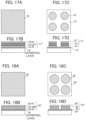
- Figs. 17A and 17B are a top view and a cross-sectional view schematically showing the structure of a PZT epitaxial growth film in step ST201 in Fig. 16 .
- Figs. 17C and 17D are a top view and a cross-sectional view schematically showing the structure of the PZT epitaxial growth film in step ST202 in Fig. 16 .
- Figs. 18A and 18B are a top view and a cross-sectional view schematically showing the structure of an AlN epitaxial growth film in step ST204 in Fig. 16 .
- FIGS. 18C and 18D are a top view and a cross-sectional view schematically showing the structure of the AlN epitaxial growth film in step ST205 in Fig. 16 .
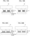
- Figs. 19A and 19B are cross-sectional views schematically showing a holding process of a plurality of PZT piezoelectric-body films 117 in step ST203 in Fig. 16 .
- Figs. 20A and 20B are cross-sectional views schematically showing a holding process of a plurality of AlN piezoelectric-body films 127 in step ST206 in Fig. 16 .
- Fig. 21A is a cross-sectional view schematically showing a sticking process of the AlN piezoelectric-body film 127 in step ST207 in Fig. 16 , and Fig.
- FIG. 21B is a top view showing a state in which the AlN piezoelectric-body film 127 has been stuck.
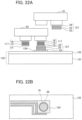
- Fig. 22A is a cross-sectional view schematically showing a sticking process of the PZT piezoelectric-body film 117 in step ST208 in Fig. 16
- Fig. 22B is a top view showing a state in which the PZT piezoelectric-body film 117 has been stuck.
- the sacrificial layer 14, a Pt film 13, the PZT film 15 and the Pt film 16 are grown epitaxially on a growth substrate as shown in Figs. 17A and 17B (step ST201), and a plurality of PZT piezoelectric-body films 117 are formed by forming the Pt film 13, the PZT film 15 and the Pt film 16 into circular shapes by means of etching as shown in Figs. 17C and 17D (step ST202) .
- the sacrificial layer 24, a Pt film 23, the AlN film 25 and the Pt film 26 are grown epitaxially on another growth substrate as shown in Figs. 18A and 18B (step ST204), and a plurality of AlN piezoelectric-body films 127 are formed by forming the Pt film 23, the AlN film 25 and the Pt film 26 into circular shapes by means of etching as shown in Figs. 18C and 18D (step ST205).
- the plurality of (4 in the illustrated example) PZT piezoelectric-body films 117 as individual pieces each formed with the Pt film 13, the PZT film 15 and the Pt film 16 are held by the stamp 42 as the holding member and are peeled off by etching the sacrificial layer (step ST203).
- the plurality of (4 in the illustrated example) AlN piezoelectric-body films 127 as individual pieces each formed with the Pt film 23, the AlN film 25 and the Pt film 26 are held by the stamp 41 as the holding member and are peeled off by etching the sacrificial layer (step ST206).
- one of the plurality of AlN piezoelectric-body films 127 held by the stamp 41 is stuck on the Pt film 134 (step ST207).
- the Pt film 134 is formed on a glass polyimide multilayer substrate 133.
- the glass polyimide multilayer substrate 133 is formed with a glass part 131 and a polyimide part 132 stacked on the glass part 131, and the Pt film 134 is formed on the polyimide part 132.
- one of the plurality of PZT piezoelectric-body films 117 held by the stamp 42 is stuck on the Pt film 26 of the AlN piezoelectric-body film 127 that has been stuck on the Pt film 134 (step ST208) . While it is desirable in the first embodiment to add the process of strengthening the sticking of Pt and each piezoelectric film by performing the annealing process after the sticking, it is unnecessary to perform the annealing process in the second embodiment since each piezoelectric-body film has structure including the Pt film 16, 26 as the upper electrode and the Pt film 13, 23 as the lower electrode.
- the contact electrodes and the wiring pattern are formed with Pt on the glass polyimide multilayer substrate 133, the AlN piezoelectric-body film 127 is stuck, and thereafter the PZT piezoelectric-body film 117 is overlaid and stuck on the Pt film 26 as the upper-electrode film of the AlN piezoelectric-body film 127.
- the AlN piezoelectric-body films 127 held by the stamp 41 are in a 2 ⁇ 2 matrix
- the AlN piezoelectric-body films 27 are successively stuck on different glass polyimide multilayer substrates 133 in the illustrated order of #1, #2, #3 and #4.
- the AlN piezoelectric-body film 127 as the piezoelectric-body film having greater diameter is stuck first.
- four glass polyimide multilayer substrates 133 are prepared for the four piezoelectric-body films.
- the PZT piezoelectric-body film 117 is stuck on the AlN piezoelectric-body film 127 as shown in Figs. 22A and 22B .
- the sticking is executed successively in the order of #1, #2, #3 and #4, and thus the stamp 42 as the holding member for sticking the PZT piezoelectric-body film 117 on the AlN piezoelectric-body film 127 is capable of executing the sticking without interfering with the AlN piezoelectric-body film 127 as shown in Fig. 23A .
- the insulation film 35a and the wiring film 36a are formed on the PZT film 15 and the Pt film 16, and the insulation film 35b and the wiring film 36b are formed on the AlN film 25 and the Pt film 26.
- the PZT piezoelectric-body film 117 and the AlN piezoelectric-body film 127 which are unlikely to grow epitaxially on the same glass polyimide multilayer substrate 133, are respectively grown epitaxially on separate growth substrates, peeled off from the growth substrates, and stuck on a common glass polyimide multilayer substrate 133 in superimposition with each other, by which a high-performance piezoelectric-body film joint substrate 200 can be made.
- the annealing process for stabilizing characteristics is necessary, and thus a plurality of piezoelectric-body films differing in the crystal structure can be provided on a non-heat-resistant substrate.
- the second embodiment is the same as the first embodiment.
Landscapes
- Engineering & Computer Science (AREA)
- Manufacturing & Machinery (AREA)
- Piezo-Electric Or Mechanical Vibrators, Or Delay Or Filter Circuits (AREA)
- Surface Acoustic Wave Elements And Circuit Networks Thereof (AREA)
Abstract
Description
- The present disclosure relates to a piezoelectric-body film joint substrate and a manufacturing method thereof.
- Conventionally, there has been proposed a device formed by stacking a plurality of piezoelectric films of different types. See
Japanese Patent Application Publication No. 2018-190890 - However, a high-performance device including a plurality of piezoelectric films cannot be obtained when a plurality of piezoelectric films of different types are stacked on the same substrate in a conventional device.
- An object of the present disclosure is to provide a high-performance piezoelectric-body film joint substrate in which piezoelectric films of two or more types are provided in superimposition with each other on the same substrate and a manufacturing method thereof.
- A piezoelectric-body film joint substrate in the present disclosure includes a substrate, a substrate electrode provided on the substrate, a first piezoelectric-body film stuck on the substrate electrode and including a first piezoelectric film and a first upper electrode film formed on the first piezoelectric film, and a second piezoelectric-body film stuck on the first upper electrode film and including a second piezoelectric film different from the first piezoelectric film and a second upper electrode film formed on the second piezoelectric film.
- A method of manufacturing a piezoelectric-body film joint substrate in the present disclosure includes peeling off a first piezoelectric-body film formed on a first substrate and including a first piezoelectric film and a first electrode film provided on the first piezoelectric film and a second piezoelectric-body film formed on a second substrate and including a second piezoelectric film and a second electrode film provided on the second piezoelectric film respectively from the first substrate and the second substrate, sticking the first piezoelectric-body film on an electrode formed on a third substrate different from both of the first substrate and the second substrate, and sticking the second piezoelectric-body film on the first piezoelectric-body film.
- According to the present disclosure, it is possible to provide a high-performance piezoelectric-body film joint substrate in which piezoelectric films of two or more types are provided in superimposition with each other on the same substrate and a manufacturing method thereof.
- The present disclosure will become more fully understood from the detailed description given hereinbelow and the accompanying drawings which are given by way of illustration only, and wherein:
-
Fig. 1 is a side view schematically showing the structure of a piezoelectric-body film joint substrate according to a first embodiment; -
Fig. 2 is a top view schematically showing the structure of the piezoelectric-body film joint substrate inFig. 1 ; -
Fig. 3 is a cross-sectional view of the piezoelectric-body film joint substrate inFig. 2 taken along the line S3-S3; -
Fig. 4 is a flowchart showing a method of manufacturing the piezoelectric-body film joint substrate according to the first embodiment; -
Figs. 5A and 5B are a top view and a cross-sectional view schematically showing the structure of a PZT epitaxial growth film in step ST101 inFig. 4 , andFigs. 5C and 5D are a top view and a cross-sectional view schematically showing the structure of the PZT epitaxial growth film in step ST102 inFig. 4 ; -
Figs. 6A and 6B are a top view and a cross-sectional view schematically showing the structure of an AlN epitaxial growth film in step ST104 inFig. 4 , andFigs. 6C and 6D are a top view and a cross-sectional view schematically showing the structure of the AlN epitaxial growth film in step ST105 inFig. 4 ; -
Figs. 7A and 7B are cross-sectional views schematically showing a holding process of a plurality of PZT piezoelectric-body films in step ST103 inFig. 4 ; -
Figs. 8A and 8B are cross-sectional views schematically showing a holding process of a plurality of AlN piezoelectric-body films in step ST106 inFig. 4 ; -
Fig. 9A is a cross-sectional view schematically showing a sticking process of the AlN piezoelectric-body film in step ST107 inFig. 4 , andFig. 9B is a top view showing a state in which the AlN piezoelectric-body film has been stuck; -
Fig. 10A is a cross-sectional view schematically showing a sticking process of the PZT piezoelectric-body film in step ST108 inFig. 4 , andFig. 10B is a top view showing a state in which the PZT piezoelectric-body film has been stuck; -
Fig. 11A is a cross-sectional view showing a manufacturing process of the next piezoelectric-body film joint substrate, andFig. 11B is a top view showing a state in which the PZT piezoelectric-body film has been stuck; -
Figs. 12A and 12B are a side view and a top view schematically showing the structure of a piezoelectric-body film joint substrate according to a modification of the first embodiment; -
Figs. 13A and 13B are a side view and a top view schematically showing the structure of a piezoelectric-body film joint substrate according to a second embodiment; -
Fig. 14 is a cross-sectional view schematically showing the structure of an epitaxial growth film including a PZT piezoelectric-body film; -
Fig. 15 is a cross-sectional view schematically showing the structure of an epitaxial growth film including an AlN piezoelectric-body film; -
Fig. 16 is a flowchart showing a method of manufacturing the piezoelectric-body film joint substrate inFigs. 13A and 13B ; -
Figs. 17A and 17B are a top view and a cross-sectional view schematically showing the structure of a PZT epitaxial growth film in step ST201 inFig. 16 , andFigs. 17C and 17D are a top view and a cross-sectional view schematically showing the structure of the PZT epitaxial growth film in step ST202 inFig. 16 ; -
Figs. 18A and 18B are a top view and a cross-sectional view schematically showing the structure of an AlN epitaxial growth film in step ST204 inFig. 16 , andFigs. 18C and 18D are a top view and a cross-sectional view schematically showing the structure of the AlN epitaxial growth film in step ST205 inFig. 16 ; -
Figs. 19A and 19B are cross-sectional views schematically showing a holding process of a plurality of PZT piezoelectric-body films in step ST203 inFig. 16 ; -
Figs. 20A and 20B are cross-sectional views schematically showing a holding process of a plurality of AlN piezoelectric-body films in step ST206 inFig. 16 ; -
Fig. 21A is a cross-sectional view schematically showing a sticking process of the AlN piezoelectric-body film in step ST207 inFig. 16 , andFig. 21B is a top view showing a state in which the AlN piezoelectric-body film has been stuck; -
Fig. 22A is a cross-sectional view schematically showing a sticking process of the PZT piezoelectric-body film in step ST208 inFig. 16 , andFig. 22B is a top view showing a state in which the PZT piezoelectric-body film has been stuck; and -
Fig. 23A is a cross-sectional view showing a manufacturing process of the next piezoelectric-body film joint substrate, andFig. 23B is a top view showing a state in which the PZT piezoelectric-body film has been stuck. - A piezoelectric-body film joint substrate and a manufacturing method thereof according to each embodiment will be described below with reference to the drawings. The following embodiments are just examples and a variety of modifications are possible within the scope of the present disclosure. In the present application, the piezoelectric-body film joint substrate is a product as an intermediate in which a plurality of piezoelectric films are provided on the same substrate. While the piezoelectric films are desired to be monocrystalline piezoelectric films, it is also possible to form the piezoelectric-body film joint substrate with polycrystalline piezoelectric films.
- By using a piezoelectric-body film joint substrate according to each embodiment, a piezoelectric film integrated device including a plurality of piezoelectric bodies can be manufactured. The piezoelectric film integrated device is an acoustic oscillation sensor, for example. Incidentally, the acoustic oscillation sensor is a sensor that detects status (e.g., distance, shape, movement or the like) of a detection target object by outputting an acoustic oscillatory wave and detecting reflected waves of the acoustic oscillatory wave. The acoustic oscillation sensor is referred to also as an "ultrasonic sensor". In general, and in the present application, the acoustic oscillatory wave is made up of at least one of a sonic wave and an ultrasonic wave. Namely, the acoustic oscillatory wave includes a sonic wave, an ultrasonic wave, or both of a sonic wave and an ultrasonic wave.
-
Fig. 1 is a side view schematically showing the structure of a piezoelectric-body filmjoint substrate 100 according to a first embodiment.Fig. 2 is a top view schematically showing the structure of the piezoelectric-body filmjoint substrate 100.Fig. 3 is a cross-sectional view of the piezoelectric-body filmjoint substrate 100 inFig. 2 taken along the line S3-S3. - The piezoelectric-body film
joint substrate 100 includes anSOI substrate 33 as a substrate and a platinum (Pt)film 34 as an electrode (i.e., substrate electrode) provided on theSOI substrate 33. As shown inFig. 2 , thePt film 34 is connected to a wiring layer formed on theSOI substrate 33. The SOI stands for Silicon On Insulator. Further, in theSOI substrate 33, there may be formed a drive circuit for driving the piezoelectric-body filmjoint substrate 100 and thereby generating the acoustic oscillatory wave, a processing circuit that executes a process by using an acoustic oscillatory wave detection signal, and so forth. - The piezoelectric-body film
joint substrate 100 includes an AlN piezoelectric-body film 27 as a first piezoelectric-body film stuck (i.e., bonded) on thePt film 34 being the substrate electrode and a PZT piezoelectric-body film 17 as a second piezoelectric-body film stuck (i.e., bonded) on the AlN piezoelectric-body film 27. The AlN piezoelectric-body film 27 includes anAlN film 25 as a first piezoelectric film and aPt film 26 as a first upper electrode film formed on theAlN film 25. The PZT piezoelectric-body film 17 includes aPZT film 15 as a second piezoelectric film different from the first piezoelectric film (e.g., in crystal structure) and aPt film 16 as a second upper electrode film formed on thePZT film 15, and is stuck on thePt film 26. Further, area of the PZT piezoelectric-body film 17 and area of the AlN piezoelectric-body film 27 differ from each other. In the first embodiment, the area of the PZT piezoelectric-body film 17 is smaller than the area of the AlN piezoelectric-body film 27. - The AlN represents aluminum nitride. The PZT represents piezoelectric zirconate titanate (lead zirconate titanate). As the first piezoelectric-body film, instead of the AlN piezoelectric-body film, a different piezoelectric film such as a lithium tantalate (LiTaO3) piezoelectric-body film or a lithium niobate (LiNbO3) piezoelectric-body film may be used. As the second piezoelectric-body film, instead of the PZT piezoelectric-body film, a different piezoelectric-body film such as a potassium sodium niobate (KNN) piezoelectric-body film or a barium titanate (BaTiO3) piezoelectric-body film may be used. Further, while the first and second piezoelectric-body films are desired to be monocrystalline piezoelectric-body films, polycrystalline piezoelectric-body films may also be used. In the illustrated example, the first piezoelectric-body film is a piezoelectric body that detects the acoustic oscillatory wave (or its reflected waves), and is a piezoelectric body having lower specific inductive capacity and higher detection sensitivity compared to the second piezoelectric-body film. The second piezoelectric-body film is a piezoelectric body that generates the acoustic oscillatory wave, and is desired to be a piezoelectric body having a higher piezoelectric constant and capable of obtaining greater oscillation amplitude compared to the first piezoelectric-body film.
- Incidentally, it is permissible even if the first piezoelectric-body film as a piezoelectric-body film on a lower side includes a PZT film and a Pt film and the second piezoelectric-body film as a piezoelectric-body film on an upper side includes an AlN film and a Pt film overlaid on the AlN film.
- Further, as shown in
Fig. 1 , the piezoelectric-body filmjoint substrate 100 includes aninsulation film 35a, awiring film 36a formed on theinsulation film 35a, aninsulation film 35b, and awiring film 36b formed on theinsulation film 35b. - The
SOI substrate 33 includes aSi substrate 30, a silicon dioxide (SiO2)part 31 as an insulation film, and a monocrystalline silicon (monocrystalline Si)part 32. A cavity (hole) may be formed by etching theSi substrate 30 in a region of themonocrystalline Si part 32 under thePZT film 15 and the AlN film 25 (i.e., region overlapping with the piezoelectric films). TheSiOz part 31 and themonocrystalline Si part 32 situated in the region where the cavity is formed have a function as a vibrating plate. Further, as the substrate, a substrate made of a different material such as a glass substrate or an organic film substrate may also be used instead of theSOI substrate 33. The acoustic oscillatory wave generated by thePZT film 15 is outputted through the cavity, and theAlN film 25 detects reflected waves of the acoustic oscillatory wave through the cavity. - The thickness of the
PZT film 15 is generally in a range of 10 nm to 10 µm, and preferably in a range of 100 nm to 5 µm. The thickness of theAlN film 25 is generally in a range of 10 nm to 10 µm, and preferably in a range of 100 nm to 2 µm. ThePt film 34 is formed on the upper surface of theSOI substrate 33. The surface (upper surface) of thePt film 34 and the AlN piezoelectric-body film 27 are joined together by intermolecular force. The surface of thePt film 26 of the AlN piezoelectric-body film 27 and the PZT piezoelectric-body film 17 are joined together by intermolecular force. For these joints, the use of an adhesive agent is unnecessary. For excellently joining these surfaces by intermolecular force, the surface roughness of a sticking surface of the AlN piezoelectric-body film 27, a sticking surface of the PZT piezoelectric-body film 17, thePt film 34 and thePt film 26 is desired to be less than or equal to 10 nm. For this purpose, processes for smoothing the surfaces of thePt film 34 and thePt film 26 may be executed. Further, an interface when the sticking surface of the AlN piezoelectric-body film 27 has been stuck on thePt film 34 is less than or equal to 10 nm. Furthermore, area of the surface of thePt film 34 is desired to be larger than area of the sticking surface of the AlN piezoelectric-body film 27. Thanks to such structure, a permissible range of a sticking accuracy error when the AlN piezoelectric-body film 27 is stuck on thePt film 34 can be made wide. - In the manufacture of the piezoelectric-body film
joint substrate 100, the AlN piezoelectric-body film 27 formed on agrowth substrate 21 and including theAlN film 25 and thePt film 26 formed on theAlN film 25 and the PZT piezoelectric-body film 17 formed on agrowth substrate 11 and including thePZT film 15 and thePt film 16 formed on thePZT film 15 are peeled off respectively from thegrowth substrates body film 27 is stuck on thePt films 34 as the electrode formed on theSOI substrate 33 different from both of thegrowth substrates body film 17 is stuck on the AlN piezoelectric-body film 27. -
Fig. 4 is a flowchart showing a method of manufacturing the piezoelectric-body filmjoint substrate 100.Figs. 5A and 5B are a top view and a cross-sectional view schematically showing the structure of a PZT epitaxial growth film in step ST101 inFig. 4 .Figs. 5C and 5D are a top view and a cross-sectional view schematically showing the structure of the PZT epitaxial growth film in step ST102 inFig. 4 .Figs. 6A and 6B are a top view and a cross-sectional view schematically showing the structure of an AlN epitaxial growth film in step ST104 inFig. 4 .Figs. 6C and 6D are a top view and a cross-sectional view schematically showing the structure of the AlN epitaxial growth film in step ST105 inFig. 4 .Figs. 7A and 7B are cross-sectional views schematically showing a holding process of a plurality of PZT piezoelectric-body films 17 in step ST103 inFig. 4 .Figs. 8A and 8B are cross-sectional views schematically showing a holding process of a plurality of AlN piezoelectric-body films 27 in step ST106 inFig. 4 .Fig. 9A is a cross-sectional view schematically showing a sticking process of the AlN piezoelectric-body film 27 in step ST107 inFig. 4 , andFig. 9B is a top view showing a state in which the AIN piezoelectric-body film 27 has been stuck.Fig. 10A is a cross-sectional view schematically showing a sticking process of the PZT piezoelectric-body film 17 in step ST108 inFig. 4 , andFig. 10B is a top view showing a state in which the PZT piezoelectric-body film 17 has been stuck.Fig. 11A is a cross-sectional view showing a manufacturing process of the next piezoelectric-body film joint. substrate, andFig. 113 is a top view showing a state in which the PZT piezoelectric-body film 17 has been stuck. - First, a
sacrificial layer 14, thePZT film 15 and thePt film 16 are grown epitaxially on a growth substrate as shown inFigs. 5A and 5B (step ST101), and a plurality of PZT piezoelectric-body films 17 are formed by forming thePZT film 15 and thePt film 16 into circular shapes by means of etching as shown inFigs. 5C and 5D (step ST102). - Further, a
sacrificial layer 24, theAlN film 25 and thePt film 26 are grown epitaxially on another growth substrate as shown inFigs. 6A and 6B (step ST104), and a plurality of AlN piezoelectric-body films 27 are formed by forming theAlN film 25 and thePt film 26 into circular shapes by means of etching as shown inFigs. 6C and 6D (step ST105). - Subsequently, as shown in
Figs. 7A and 7B , the plurality of (4 in the illustrated example) PZT piezoelectric-body films 17 as individual pieces each formed with thePZT film 15 and thePt film 16 are held by astamp 42 as a holding member and are peeled off by etching the sacrificial layer (step ST103). Further, as shown inFigs. 8A and 8B , the plurality of (4 in the illustrated example) AlN piezoelectric-body films 27 as individual pieces each formed with theAlN film 25 and thePt film 26 are held by astamp 41 as a holding member and are peeled off by etching the sacrificial layer (step ST106). - Subsequently, as shown in
Figs. 9A and 9B , one of the plurality of AlN piezoelectric-body films 27 held by thestamp 41 is stuck on the Pt film 34 (step ST107). - Subsequently, as shown in
Figs. 10A and 10B , one of the plurality of PZT piezoelectric-body films 17 held by thestamp 42 is stuck on thePt film 26 of the AlN piezoelectric-body film 27 that has been stuck on the Pt film 34 (step ST108). It is also possible to add a process of strengthening the sticking of Pt and each piezoelectric film by performing an annealing process after the sticking. - As shown in
Figs. 9A and 9B , in the first embodiment, contact electrodes and a wiring pattern are formed with Pt on theSOI substrate 33, the AlN piezoelectric-body film 27 is stuck, and thereafter the PZT piezoelectric-body film 17 is overlaid and stuck on thePt film 26 as the upper electrode film of the AlN piezoelectric-body film 27. In cases where the AlN piezoelectric-body films 27 held by thestamp 41 are in a 2 × 2 matrix, the AIN piezoelectric-body films 27 are successively stuck ondifferent SOI substrates 33 in the illustrated order of #1, #2, #3 and #4. In this case, the AIN piezoelectric-body film 27 as the piezoelectric-body film having greater diameter is stuck first. In this example, fourSOI substrates 33 are prepared for the four piezoelectric-body films. The PZT piezoelectric-body film 17 is stuck on the AlN piezoelectric-body film 27 as shown inFigs. 10A and 10B . The sticking is executed successively in the order of #1, #2, #3 and #4, and thus thestamp 42 as the holding member for sticking the PZT piezoelectric-body film 17 on the AlN piezoelectric-body film 27 is capable of executing the sticking without interfering with the AlN piezoelectric-body film 27 as shown inFig. 11A . - Subsequently, the
insulation film 35a and thewiring film 36a are formed on thePZT film 15 and thePt film 16, and theinsulation film 35b and thewiring film 36b are formed on theAlN film 25 and thePt film 26. - At the time of the sticking, the hexagonal crystal of AlN and the cubic crystal of PZT are arranged in a phase relationship so that their c-axes are parallel to each other, by which efficiency of the piezoelectric oscillation driving of the
PZT film 15 and the piezoelectric oscillation reception of theAlN film 25 is maximized. -
Figs. 12A and 12B are a side view and a top view schematically showing the structure of a piezoelectric-body filmjoint substrate 100a according to a modification of the first embodiment. The piezoelectric-body film,joint substrate 100a differs from the piezoelectric-body filmjoint substrate 100 shown inFig. 1 to Fig. 3 in that the two-dimensional shape of each of an AlN piezoelectric-body film 27a and a PZT piezoelectric-body film 17a is a quadrangular shape. Except for this feature, the piezoelectric-body filmjoint substrate 100a is the same as the piezoelectric-body filmjoint substrate 100. - As described above, in the first embodiment, the PZT piezoelectric-
body film 17 and the AlN piezoelectric-body film 27, which are unlikely to grow epitaxially on thesame SOI substrate 33 because of the difference in the lattice constant and the crystal structure, are respectively formed on separate growth substrates, peeled off from the growth substrates, and stuck on acommon SOI substrate 33 in superimposition with each other, by which a high-performance piezoelectric-body filmjoint substrate 100 can be made. - Further, since the
PZT film 15 being monocrystalline has a higher piezoelectric constant compared to a polycrystalline PZT film, amplitude of the oscillation can be increased with ease. Furthermore, since theAlN film 25 being monocrystalline has lower specific inductive capacity compared to a polycrystalline AlN film, the oscillation reception sensitivity can be increased. However, thePZT film 15 may contain polycrystalline PZT, and theAlN film 25 may contain polycrystalline AlN. Namely, monocrystallization ratios of thePZT film 15 and theAlN film 25 may be less than or equal to 100%. - Furthermore, conventionally, in order to form piezoelectric films of different types, a process like temporarily covering one piezoelectric film with a protective layer, forming the other piezoelectric film, and thereafter removing the protective layer used to be a complicated process, and application of heat in processing in each step used to leave residual stress distortion in the piezoelectric films and cause deterioration in the efficiency of the sensor. By the manufacturing method in the first embodiment, the piezoelectric-body film joint substrate and the acoustic oscillation sensor can be formed in a state with no residual stress distortion.
-
Figs. 13A and 13B are a side view and a top view schematically showing the structure of a piezoelectric-body filmjoint substrate 200 according to a second embodiment. InFigs. 13A and 13B , each component identical or corresponding to a component shown inFig. 1 to Fig. 3 is assigned the same reference character as inFig. 1 to Fig. 3 . - The piezoelectric-body film
joint substrate 200 includes an AlN piezoelectric-body film 127 as a first piezoelectric-body film stuck on aPt film 134 and a PZT piezoelectric-body film 117 as a second piezoelectric-body film stuck on the AlN piezoelectric-body film 127. The AlN piezoelectric-body film 127 includes aPt film 126 as a first lower electrode film, theAlN film 25 as a first piezoelectric film formed on thePt film 126, and thePt film 26 as a first upper electrode film formed on theAlN film 25. The PZT piezoelectric-body film 117 includes aPt film 116 as a second lower electrode film, thePZT film 15 as a second piezoelectric film different from the first piezoelectric film (e.g., in crystal structure), and thePt film 16 as a second upper electrode film formed on thePZT film 15, and thePt film 116 is stuck on thePt film 26. Further, area of the PZT piezoelectric-body film 117 and area of the AlN piezoelectric-body film 127 differ from each other. In the second embodiment, the area of the PZT piezoelectric-body film 117 is smaller than the area of the AlN piezoelectric-body film 127. Except for the above-described features, the structure of the piezoelectric-body filmjoint substrate 200 is the same as that of the piezoelectric-body filmjoint substrate 100. While the substrate electrode is formed with Pt (platinum) in this example, it is not particularly necessary to limit the material of the substrate electrode to Pt. For example, the substrate electrode may be formed with a variety of metal such as gold, aluminum or copper. -
Fig. 14 is a cross-sectional view schematically showing the structure of an epitaxial growth film including the PZT piezoelectric-body film 117.Fig. 15 is a cross-sectional view schematically showing the structure of an epitaxial growth film including the AlN piezoelectric-body film 127. In the manufacture of the piezoelectric-body filmjoint substrate 200, the AlN piezoelectric-body film 127 as the first piezoelectric-body film formed on thegrowth substrate 21 and including thePt film 126, theAlN film 25 and thePt film 26 and the PZT piezoelectric-body film 117 formed on thegrowth substrate 11 and including thePt film 116, thePZT film 15 and thePt film 16 are peeled off respectively from thegrowth substrates body film 127 is stuck on thePt films 134 formed on theSOI substrate 33 different from both of thegrowth substrates body film 117 is stuck on the AlN piezoelectric-body film 127. -
Fig. 16 is a flowchart showing a method of manufacturing the piezoelectric-body filmjoint substrate 200.Figs. 17A and 17B are a top view and a cross-sectional view schematically showing the structure of a PZT epitaxial growth film in step ST201 inFig. 16 .Figs. 17C and 17D are a top view and a cross-sectional view schematically showing the structure of the PZT epitaxial growth film in step ST202 inFig. 16 .Figs. 18A and 18B are a top view and a cross-sectional view schematically showing the structure of an AlN epitaxial growth film in step ST204 inFig. 16 .Figs. 18C and 18D are a top view and a cross-sectional view schematically showing the structure of the AlN epitaxial growth film in step ST205 inFig. 16 .Figs. 19A and 19B are cross-sectional views schematically showing a holding process of a plurality of PZT piezoelectric-body films 117 in step ST203 inFig. 16 .Figs. 20A and 20B are cross-sectional views schematically showing a holding process of a plurality of AlN piezoelectric-body films 127 in step ST206 inFig. 16 .Fig. 21A is a cross-sectional view schematically showing a sticking process of the AlN piezoelectric-body film 127 in step ST207 inFig. 16 , andFig. 21B is a top view showing a state in which the AlN piezoelectric-body film 127 has been stuck.Fig. 22A is a cross-sectional view schematically showing a sticking process of the PZT piezoelectric-body film 117 in step ST208 inFig. 16 , andFig. 22B is a top view showing a state in which the PZT piezoelectric-body film 117 has been stuck. - First, the
sacrificial layer 14, aPt film 13, thePZT film 15 and thePt film 16 are grown epitaxially on a growth substrate as shown inFigs. 17A and 17B (step ST201), and a plurality of PZT piezoelectric-body films 117 are formed by forming thePt film 13, thePZT film 15 and thePt film 16 into circular shapes by means of etching as shown inFigs. 17C and 17D (step ST202) . - Further, the
sacrificial layer 24, aPt film 23, theAlN film 25 and thePt film 26 are grown epitaxially on another growth substrate as shown inFigs. 18A and 18B (step ST204), and a plurality of AlN piezoelectric-body films 127 are formed by forming thePt film 23, theAlN film 25 and thePt film 26 into circular shapes by means of etching as shown inFigs. 18C and 18D (step ST205). - Subsequently, as shown in
Figs. 19A and 19B , the plurality of (4 in the illustrated example) PZT piezoelectric-body films 117 as individual pieces each formed with thePt film 13, thePZT film 15 and thePt film 16 are held by thestamp 42 as the holding member and are peeled off by etching the sacrificial layer (step ST203). Further, as shown inFigs. 20A and 20B , the plurality of (4 in the illustrated example) AlN piezoelectric-body films 127 as individual pieces each formed with thePt film 23, theAlN film 25 and thePt film 26 are held by thestamp 41 as the holding member and are peeled off by etching the sacrificial layer (step ST206). - Subsequently, as shown in
Figs. 21A and 21B , one of the plurality of AlN piezoelectric-body films 127 held by thestamp 41 is stuck on the Pt film 134 (step ST207). In the second embodiment, an example in which thePt film 134 is formed on a glasspolyimide multilayer substrate 133 is shown. The glasspolyimide multilayer substrate 133 is formed with aglass part 131 and apolyimide part 132 stacked on theglass part 131, and thePt film 134 is formed on thepolyimide part 132. - Subsequently, as shown in
Figs. 22A and 22B , one of the plurality of PZT piezoelectric-body films 117 held by thestamp 42 is stuck on thePt film 26 of the AlN piezoelectric-body film 127 that has been stuck on the Pt film 134 (step ST208) . While it is desirable in the first embodiment to add the process of strengthening the sticking of Pt and each piezoelectric film by performing the annealing process after the sticking, it is unnecessary to perform the annealing process in the second embodiment since each piezoelectric-body film has structure including thePt film Pt film - As shown in
Figs. 23A and 23B , in the second embodiment, the contact electrodes and the wiring pattern are formed with Pt on the glasspolyimide multilayer substrate 133, the AlN piezoelectric-body film 127 is stuck, and thereafter the PZT piezoelectric-body film 117 is overlaid and stuck on thePt film 26 as the upper-electrode film of the AlN piezoelectric-body film 127. In cases where the AlN piezoelectric-body films 127 held by thestamp 41 are in a 2 × 2 matrix, the AlN piezoelectric-body films 27 are successively stuck on different glasspolyimide multilayer substrates 133 in the illustrated order of #1, #2, #3 and #4. In this case, the AlN piezoelectric-body film 127 as the piezoelectric-body film having greater diameter is stuck first. In this example, four glasspolyimide multilayer substrates 133 are prepared for the four piezoelectric-body films. The PZT piezoelectric-body film 117 is stuck on the AlN piezoelectric-body film 127 as shown inFigs. 22A and 22B . The sticking is executed successively in the order of #1, #2, #3 and #4, and thus thestamp 42 as the holding member for sticking the PZT piezoelectric-body film 117 on the AlN piezoelectric-body film 127 is capable of executing the sticking without interfering with the AlN piezoelectric-body film 127 as shown inFig. 23A . - Subsequently, the
insulation film 35a and thewiring film 36a are formed on thePZT film 15 and thePt film 16, and theinsulation film 35b and thewiring film 36b are formed on theAlN film 25 and thePt film 26. - As described above, in the second embodiment, the PZT piezoelectric-
body film 117 and the AlN piezoelectric-body film 127, which are unlikely to grow epitaxially on the same glasspolyimide multilayer substrate 133, are respectively grown epitaxially on separate growth substrates, peeled off from the growth substrates, and stuck on a common glasspolyimide multilayer substrate 133 in superimposition with each other, by which a high-performance piezoelectric-body filmjoint substrate 200 can be made. - Further, according to the manufacturing method in the second embodiment, the annealing process for stabilizing characteristics is necessary, and thus a plurality of piezoelectric-body films differing in the crystal structure can be provided on a non-heat-resistant substrate.
- Incidentally, except for the above-described features, the second embodiment is the same as the first embodiment.
- 100, 100a, 200: piezoelectric-body film joint substrate, 11, 21: growth substrate (monocrystalline Si substrate), 15: PZT film (second piezoelectric film), 16: Pt film (second upper electrode film), 13: Pt film (second lower electrode film), 14, 24: sacrificial layer, 17, 117: PZT piezoelectric-body film (second piezoelectric-body film), 23: Pt film (first lower electrode film), 25: AlN film (first piezoelectric film), 26: Pt film (first upper electrode film), 27, 127: AlN piezoelectric-body film (first piezoelectric-body film), 31: SiO2 part, 32: monocrystalline Si part, 33: SOI substrate (substrate), 34, 134: Pt film (substrate electrode), 116: Pt film, 126: Pt film, 133: glass polyimide multilayer substrate.
Claims (13)
- A piezoelectric-body film joint substrate (100, 200) comprising:a substrate (33);a substrate electrode (34) provided on the substrate (33);a first piezoelectric-body film (27) stuck on the substrate electrode (34) and including a first piezoelectric film (25) and a first upper electrode film (26) formed on the first piezoelectric film (25); anda second piezoelectric-body film (17) stuck on the first upper electrode film (26) and including a second piezoelectric film (15) different from the first piezoelectric film (25) and a second upper electrode film (16) formed on the second piezoelectric film (15).
- The piezoelectric-body film joint substrate (100, 200) according to claim 1, wherein area of the first piezoelectric-body film (27) and area of the second piezoelectric-body film (17) differ from each other.
- The piezoelectric-body film joint substrate (100, 200) according to claim 1 or 2, wherein the area of the second piezoelectric-body film (17) is smaller than the area of the first piezoelectric-body film (27).
- The piezoelectric-body film joint substrate (200) according to any one of claims 1 to 3, wherein the second piezoelectric-body film (17) further includes a second lower electrode film (13) formed on a surface of the second piezoelectric film (15) on a side opposite to the second upper electrode film (16).
- The piezoelectric-body film joint substrate (200) according to any one of claims 1 to 4, wherein the first piezoelectric-body film (27) further includes a first lower electrode film (23) formed on a surface of the first piezoelectric film (25) on a side opposite to the first upper electrode film (26).
- The piezoelectric-body film joint substrate (100, 200) according to any one of claims 1 to 5, wherein the second piezoelectric film (15) is monocrystalline and the first piezoelectric film (25) is monocrystalline.
- The piezoelectric-body film joint substrate (100, 200) according to any one of claims 1 to 6, wherein area of a surface of the substrate electrode (34) is larger than area of a sticking surface of the first piezoelectric-body film (27) stuck on the surface of the substrate electrode (34).
- The piezoelectric-body film joint substrate (100, 200) according to any one of claims 1 to 7, whereinthe first piezoelectric film (25) is an AlN film, a lithium tantalate film or a lithium niobate film, andthe second piezoelectric film (15) is a PZT film, a KNN film or a barium titanate film.
- A method of manufacturing a piezoelectric-body film joint substrate (100, 200), the method comprising:peeling off a first piezoelectric-body film (27) formed on a first substrate (21) and including a first piezoelectric film (25) and a first electrode film (26) provided on the first piezoelectric film (25) and a second piezoelectric-body film (17) formed on a second substrate (11) and including a second piezoelectric film (15) and a second electrode film provided on the second piezoelectric film (15) respectively from the first substrate (21) and the second substrate (11);sticking the first piezoelectric-body film (27) on an electrode formed on a third substrate different from both of the first substrate (21) and the second substrate (11); andsticking the second piezoelectric-body film (17) on the first piezoelectric-body film (27).
- The method of manufacturing a piezoelectric-body film joint substrate (200) according to claim 9, wherein the second piezoelectric-body film (17) further includes a second lower electrode film (23) formed on a surface of the second piezoelectric film (15) on a side opposite to the second electrode film.
- The method of manufacturing a piezoelectric-body film joint substrate (200) according to claim 9 or 10, wherein the first piezoelectric-body film (27) further includes a first lower electrode film (23) formed on a surface of the first piezoelectric film (25) on a side opposite to the first electrode film (26).
- The method of manufacturing a piezoelectric-body film joint substrate (100, 200) according to any one of claims 9 to 11, wherein the second piezoelectric film (15) is monocrystalline and the first piezoelectric film (25) is monocrystalline.
- The method of manufacturing a piezoelectric-body film joint substrate (100, 200) according to any one of claims 9 to 12, wherein area of a surface of the electrode formed on the third substrate is larger than area of a sticking surface of the first piezoelectric-body film (27) to be stuck on the surface of the electrode.
Applications Claiming Priority (1)
| Application Number | Priority Date | Filing Date | Title |
|---|---|---|---|
| JP2022055593A JP7806582B2 (en) | 2022-03-30 | 2022-03-30 | Manufacturing method of piezoelectric film bonded substrate |
Publications (3)
| Publication Number | Publication Date |
|---|---|
| EP4255160A1 true EP4255160A1 (en) | 2023-10-04 |
| EP4255160C0 EP4255160C0 (en) | 2025-08-27 |
| EP4255160B1 EP4255160B1 (en) | 2025-08-27 |
Family
ID=85556246
Family Applications (1)
| Application Number | Title | Priority Date | Filing Date |
|---|---|---|---|
| EP23160680.7A Active EP4255160B1 (en) | 2022-03-30 | 2023-03-08 | Piezoelectric-body film joint substrate and manufacturing method thereof |
Country Status (4)
| Country | Link |
|---|---|
| US (1) | US20230320217A1 (en) |
| EP (1) | EP4255160B1 (en) |
| JP (1) | JP7806582B2 (en) |
| CN (1) | CN116896970A (en) |
Families Citing this family (1)
| Publication number | Priority date | Publication date | Assignee | Title |
|---|---|---|---|---|
| WO2026141097A1 (en) * | 2024-12-27 | 2026-07-02 | 富士フイルム株式会社 | Piezoelectric laminate and piezoelectric element |
Citations (5)
| Publication number | Priority date | Publication date | Assignee | Title |
|---|---|---|---|---|
| US20130162106A1 (en) * | 2010-10-01 | 2013-06-27 | Panasonic Corporation | Vibration power generation element and vibration power generation device including same |
| US20180069168A1 (en) * | 2015-04-30 | 2018-03-08 | Murata Manufacturing Co, Ltd. | Piezoelectric device, piezoelectric transformer, and method of manufacturing piezoelectric device |
| US20180123017A1 (en) * | 2015-06-30 | 2018-05-03 | Fujifilm Corporation | Laminate structure, piezoelectric element, and method of manufacturing piezoelectric element |
| JP2018170343A (en) * | 2017-03-29 | 2018-11-01 | ローム株式会社 | Piezoelectric element and method of manufacturing the same |
| JP2018190890A (en) | 2017-05-10 | 2018-11-29 | 株式会社サイオクス | Multilayer substrate having piezoelectric film, element having piezoelectric film, and method of manufacturing multilayer substrate having piezoelectric film |
Family Cites Families (5)
| Publication number | Priority date | Publication date | Assignee | Title |
|---|---|---|---|---|
| JP5024812B2 (en) | 2006-06-20 | 2012-09-12 | 独立行政法人産業技術総合研究所 | Dielectric structure and manufacturing method thereof |
| JP5836754B2 (en) | 2011-10-04 | 2015-12-24 | 富士フイルム株式会社 | Piezoelectric element and manufacturing method thereof |
| JP7473774B2 (en) | 2019-09-12 | 2024-04-24 | ミツミ電機株式会社 | Piezoelectric actuator, optical scanning device |
| JP7568417B2 (en) | 2020-04-06 | 2024-10-16 | 住友化学株式会社 | Manufacturing method of piezoelectric laminate |
| CN114070254B (en) * | 2020-08-06 | 2025-11-07 | 诺思(天津)微系统有限责任公司 | Semiconductor structure with redundant structure, manufacturing method and electronic equipment |
-
2022
- 2022-03-30 JP JP2022055593A patent/JP7806582B2/en active Active
-
2023
- 2023-03-03 CN CN202310205783.6A patent/CN116896970A/en active Pending
- 2023-03-08 EP EP23160680.7A patent/EP4255160B1/en active Active
- 2023-03-09 US US18/181,093 patent/US20230320217A1/en active Pending
Patent Citations (5)
| Publication number | Priority date | Publication date | Assignee | Title |
|---|---|---|---|---|
| US20130162106A1 (en) * | 2010-10-01 | 2013-06-27 | Panasonic Corporation | Vibration power generation element and vibration power generation device including same |
| US20180069168A1 (en) * | 2015-04-30 | 2018-03-08 | Murata Manufacturing Co, Ltd. | Piezoelectric device, piezoelectric transformer, and method of manufacturing piezoelectric device |
| US20180123017A1 (en) * | 2015-06-30 | 2018-05-03 | Fujifilm Corporation | Laminate structure, piezoelectric element, and method of manufacturing piezoelectric element |
| JP2018170343A (en) * | 2017-03-29 | 2018-11-01 | ローム株式会社 | Piezoelectric element and method of manufacturing the same |
| JP2018190890A (en) | 2017-05-10 | 2018-11-29 | 株式会社サイオクス | Multilayer substrate having piezoelectric film, element having piezoelectric film, and method of manufacturing multilayer substrate having piezoelectric film |
Also Published As
| Publication number | Publication date |
|---|---|
| JP2023147857A (en) | 2023-10-13 |
| US20230320217A1 (en) | 2023-10-05 |
| CN116896970A (en) | 2023-10-17 |
| JP7806582B2 (en) | 2026-01-27 |
| EP4255160C0 (en) | 2025-08-27 |
| EP4255160B1 (en) | 2025-08-27 |
Similar Documents
| Publication | Publication Date | Title |
|---|---|---|
| US11495728B2 (en) | Piezoelectric device and method of manufacturing piezoelectric device | |
| US10361677B2 (en) | Transverse bulk acoustic wave filter | |
| CN111146327A (en) | Single crystal piezoelectric structure, method for manufacturing same, and electronic device having single crystal piezoelectric laminated structure | |
| US20210193901A1 (en) | Piezoelectric transducer | |
| CN114955976B (en) | A MEMS device and a method for manufacturing the same | |
| US20250113738A1 (en) | Semiconductor structure and manufacturing method thereof | |
| EP4255160B1 (en) | Piezoelectric-body film joint substrate and manufacturing method thereof | |
| CN111146328A (en) | Single crystal piezoelectric structure and electronic device having the same | |
| WO2021053884A1 (en) | Piezoelectric element and method for producing same | |
| EP4255159A1 (en) | Piezoelectric-body film joint substrate and manufacturing method thereof | |
| EP4154328B1 (en) | Integration of semiconductor membranes with piezoelectric substrates | |
| CN117548318A (en) | PMUT structure with supporting layer and manufacturing method thereof | |
| JP7863811B2 (en) | Piezoelectric film integrated device, method for manufacturing the same, and acoustic vibration sensor | |
| EP4255157A1 (en) | Piezoelectric film integrated device, manufacturing method thereof, and acoustic oscillation sensor | |
| CN117548320A (en) | Micromechanical ultrasonic transducer structure with dual PMUTs on the same side of the base and manufacturing method thereof | |
| US7969073B2 (en) | Tangentially poled single crystal ring resonator | |
| US11784629B2 (en) | Piezoelectric device | |
| TW202220240A (en) | Composite structure for mems applications, comprising a deformable layer and a piezoelectric layer, and associated fabrication process | |
| JP7216623B2 (en) | semiconductor chip | |
| JP2004198421A (en) | Piezoelectric transducer | |
| WO2024027732A1 (en) | Micromachined ultrasonic transducer structure having dual bearing layers and manufacturing method therefor | |
| CN120639048A (en) | Bulk acoustic wave resonator and manufacturing method thereof | |
| JPWO2024106543A5 (en) | ||
| JP2001016068A (en) | Piezoelectric resonator | |
| JP2007107990A (en) | Acceleration sensor |
Legal Events
| Date | Code | Title | Description |
|---|---|---|---|
| PUAI | Public reference made under article 153(3) epc to a published international application that has entered the european phase |
Free format text: ORIGINAL CODE: 0009012 |
|
| STAA | Information on the status of an ep patent application or granted ep patent |
Free format text: STATUS: THE APPLICATION HAS BEEN PUBLISHED |
|
| AK | Designated contracting states |
Kind code of ref document: A1 Designated state(s): AL AT BE BG CH CY CZ DE DK EE ES FI FR GB GR HR HU IE IS IT LI LT LU LV MC ME MK MT NL NO PL PT RO RS SE SI SK SM TR |
|
| STAA | Information on the status of an ep patent application or granted ep patent |
Free format text: STATUS: REQUEST FOR EXAMINATION WAS MADE |
|
| 17P | Request for examination filed |
Effective date: 20240301 |
|
| RBV | Designated contracting states (corrected) |
Designated state(s): AL AT BE BG CH CY CZ DE DK EE ES FI FR GB GR HR HU IE IS IT LI LT LU LV MC ME MK MT NL NO PL PT RO RS SE SI SK SM TR |
|
| STAA | Information on the status of an ep patent application or granted ep patent |
Free format text: STATUS: EXAMINATION IS IN PROGRESS |
|
| 17Q | First examination report despatched |
Effective date: 20240722 |
|
| GRAP | Despatch of communication of intention to grant a patent |
Free format text: ORIGINAL CODE: EPIDOSNIGR1 |
|
| STAA | Information on the status of an ep patent application or granted ep patent |
Free format text: STATUS: GRANT OF PATENT IS INTENDED |
|
| INTG | Intention to grant announced |
Effective date: 20250506 |
|
| RIN1 | Information on inventor provided before grant (corrected) |
Inventor name: KITAJIMA, YUTAKA Inventor name: ISHIKAWA, TAKUMA Inventor name: TANIGAWA, KENICHI Inventor name: SUZUKI, TAKAHITO Inventor name: KOSAKA, TORU Inventor name: FURUTA, HIRONORI |
|
| GRAS | Grant fee paid |
Free format text: ORIGINAL CODE: EPIDOSNIGR3 |
|
| GRAA | (expected) grant |
Free format text: ORIGINAL CODE: 0009210 |
|
| STAA | Information on the status of an ep patent application or granted ep patent |
Free format text: STATUS: THE PATENT HAS BEEN GRANTED |
|
| AK | Designated contracting states |
Kind code of ref document: B1 Designated state(s): AL AT BE BG CH CY CZ DE DK EE ES FI FR GB GR HR HU IE IS IT LI LT LU LV MC ME MK MT NL NO PL PT RO RS SE SI SK SM TR |
|
| REG | Reference to a national code |
Ref country code: CH Ref legal event code: EP |
|
| REG | Reference to a national code |
Ref country code: IE Ref legal event code: FG4D |
|
| U01 | Request for unitary effect filed |
Effective date: 20250902 |
|
| U07 | Unitary effect registered |
Designated state(s): AT BE BG DE DK EE FI FR IT LT LU LV MT NL PT RO SE SI Effective date: 20250908 |
|
| PG25 | Lapsed in a contracting state [announced via postgrant information from national office to epo] |
Ref country code: IS Free format text: LAPSE BECAUSE OF FAILURE TO SUBMIT A TRANSLATION OF THE DESCRIPTION OR TO PAY THE FEE WITHIN THE PRESCRIBED TIME-LIMIT Effective date: 20251227 |
|
| PG25 | Lapsed in a contracting state [announced via postgrant information from national office to epo] |
Ref country code: NO Free format text: LAPSE BECAUSE OF FAILURE TO SUBMIT A TRANSLATION OF THE DESCRIPTION OR TO PAY THE FEE WITHIN THE PRESCRIBED TIME-LIMIT Effective date: 20251127 |
|
| PG25 | Lapsed in a contracting state [announced via postgrant information from national office to epo] |
Ref country code: HR Free format text: LAPSE BECAUSE OF FAILURE TO SUBMIT A TRANSLATION OF THE DESCRIPTION OR TO PAY THE FEE WITHIN THE PRESCRIBED TIME-LIMIT Effective date: 20250827 |
|
| PG25 | Lapsed in a contracting state [announced via postgrant information from national office to epo] |
Ref country code: GR Free format text: LAPSE BECAUSE OF FAILURE TO SUBMIT A TRANSLATION OF THE DESCRIPTION OR TO PAY THE FEE WITHIN THE PRESCRIBED TIME-LIMIT Effective date: 20251128 |
|
| PG25 | Lapsed in a contracting state [announced via postgrant information from national office to epo] |
Ref country code: PL Free format text: LAPSE BECAUSE OF FAILURE TO SUBMIT A TRANSLATION OF THE DESCRIPTION OR TO PAY THE FEE WITHIN THE PRESCRIBED TIME-LIMIT Effective date: 20250827 |
|
| PG25 | Lapsed in a contracting state [announced via postgrant information from national office to epo] |
Ref country code: RS Free format text: LAPSE BECAUSE OF FAILURE TO SUBMIT A TRANSLATION OF THE DESCRIPTION OR TO PAY THE FEE WITHIN THE PRESCRIBED TIME-LIMIT Effective date: 20251127 |
|
| PG25 | Lapsed in a contracting state [announced via postgrant information from national office to epo] |
Ref country code: ES Free format text: LAPSE BECAUSE OF FAILURE TO SUBMIT A TRANSLATION OF THE DESCRIPTION OR TO PAY THE FEE WITHIN THE PRESCRIBED TIME-LIMIT Effective date: 20250827 |
|
| PG25 | Lapsed in a contracting state [announced via postgrant information from national office to epo] |
Ref country code: SM Free format text: LAPSE BECAUSE OF FAILURE TO SUBMIT A TRANSLATION OF THE DESCRIPTION OR TO PAY THE FEE WITHIN THE PRESCRIBED TIME-LIMIT Effective date: 20250827 |
|
| PG25 | Lapsed in a contracting state [announced via postgrant information from national office to epo] |
Ref country code: CZ Free format text: LAPSE BECAUSE OF FAILURE TO SUBMIT A TRANSLATION OF THE DESCRIPTION OR TO PAY THE FEE WITHIN THE PRESCRIBED TIME-LIMIT Effective date: 20250827 |
|
| PG25 | Lapsed in a contracting state [announced via postgrant information from national office to epo] |
Ref country code: SK Free format text: LAPSE BECAUSE OF FAILURE TO SUBMIT A TRANSLATION OF THE DESCRIPTION OR TO PAY THE FEE WITHIN THE PRESCRIBED TIME-LIMIT Effective date: 20250827 |
|
| U20 | Renewal fee for the european patent with unitary effect paid |
Year of fee payment: 4 Effective date: 20260331 |
|
| PLBE | No opposition filed within time limit |
Free format text: ORIGINAL CODE: 0009261 |
|
| STAA | Information on the status of an ep patent application or granted ep patent |
Free format text: STATUS: NO OPPOSITION FILED WITHIN TIME LIMIT |
|
| REG | Reference to a national code |
Ref country code: CH Ref legal event code: L10 Free format text: ST27 STATUS EVENT CODE: U-0-0-L10-L00 (AS PROVIDED BY THE NATIONAL OFFICE) Effective date: 20260708 |
|
| 26N | No opposition filed |
Effective date: 20260528 |