EP4254930A1 - Image sensor, camera module and electronic device - Google Patents
Image sensor, camera module and electronic device Download PDFInfo
- Publication number
- EP4254930A1 EP4254930A1 EP21897009.3A EP21897009A EP4254930A1 EP 4254930 A1 EP4254930 A1 EP 4254930A1 EP 21897009 A EP21897009 A EP 21897009A EP 4254930 A1 EP4254930 A1 EP 4254930A1
- Authority
- EP
- European Patent Office
- Prior art keywords
- pixel
- amplifier
- sub
- image sensor
- target
- Prior art date
- Legal status (The legal status is an assumption and is not a legal conclusion. Google has not performed a legal analysis and makes no representation as to the accuracy of the status listed.)
- Granted
Links
Images

Classifications
-
- H—ELECTRICITY
- H04—ELECTRIC COMMUNICATION TECHNIQUE
- H04N—PICTORIAL COMMUNICATION, e.g. TELEVISION
- H04N23/00—Cameras or camera modules comprising electronic image sensors; Control thereof
- H04N23/50—Constructional details
- H04N23/54—Mounting of pick-up tubes, electronic image sensors, deviation or focusing coils
-
- H—ELECTRICITY
- H04—ELECTRIC COMMUNICATION TECHNIQUE
- H04N—PICTORIAL COMMUNICATION, e.g. TELEVISION
- H04N25/00—Circuitry of solid-state image sensors [SSIS]; Control thereof
- H04N25/70—SSIS architectures; Circuits associated therewith
- H04N25/76—Addressed sensors, e.g. MOS or CMOS sensors
- H04N25/77—Pixel circuitry, e.g. memories, A/D converters, pixel amplifiers, shared circuits or shared components
- H04N25/778—Pixel circuitry, e.g. memories, A/D converters, pixel amplifiers, shared circuits or shared components comprising amplifiers shared between a plurality of pixels, i.e. at least one part of the amplifier must be on the sensor array itself
-
- H—ELECTRICITY
- H04—ELECTRIC COMMUNICATION TECHNIQUE
- H04N—PICTORIAL COMMUNICATION, e.g. TELEVISION
- H04N23/00—Cameras or camera modules comprising electronic image sensors; Control thereof
- H04N23/50—Constructional details
- H04N23/55—Optical parts specially adapted for electronic image sensors; Mounting thereof
-
- H—ELECTRICITY
- H04—ELECTRIC COMMUNICATION TECHNIQUE
- H04N—PICTORIAL COMMUNICATION, e.g. TELEVISION
- H04N23/00—Cameras or camera modules comprising electronic image sensors; Control thereof
- H04N23/57—Mechanical or electrical details of cameras or camera modules specially adapted for being embedded in other devices
-
- H—ELECTRICITY
- H04—ELECTRIC COMMUNICATION TECHNIQUE
- H04N—PICTORIAL COMMUNICATION, e.g. TELEVISION
- H04N23/00—Cameras or camera modules comprising electronic image sensors; Control thereof
- H04N23/60—Control of cameras or camera modules
- H04N23/61—Control of cameras or camera modules based on recognised objects
- H04N23/611—Control of cameras or camera modules based on recognised objects where the recognised objects include parts of the human body
-
- H—ELECTRICITY
- H04—ELECTRIC COMMUNICATION TECHNIQUE
- H04N—PICTORIAL COMMUNICATION, e.g. TELEVISION
- H04N23/00—Cameras or camera modules comprising electronic image sensors; Control thereof
- H04N23/70—Circuitry for compensating brightness variation in the scene
- H04N23/71—Circuitry for evaluating the brightness variation
-
- H—ELECTRICITY
- H04—ELECTRIC COMMUNICATION TECHNIQUE
- H04N—PICTORIAL COMMUNICATION, e.g. TELEVISION
- H04N23/00—Cameras or camera modules comprising electronic image sensors; Control thereof
- H04N23/70—Circuitry for compensating brightness variation in the scene
- H04N23/76—Circuitry for compensating brightness variation in the scene by influencing the image signals
-
- H—ELECTRICITY
- H04—ELECTRIC COMMUNICATION TECHNIQUE
- H04N—PICTORIAL COMMUNICATION, e.g. TELEVISION
- H04N25/00—Circuitry of solid-state image sensors [SSIS]; Control thereof
- H04N25/10—Circuitry of solid-state image sensors [SSIS]; Control thereof for transforming different wavelengths into image signals
-
- H—ELECTRICITY
- H04—ELECTRIC COMMUNICATION TECHNIQUE
- H04N—PICTORIAL COMMUNICATION, e.g. TELEVISION
- H04N25/00—Circuitry of solid-state image sensors [SSIS]; Control thereof
- H04N25/50—Control of the SSIS exposure
- H04N25/51—Control of the gain
-
- H—ELECTRICITY
- H04—ELECTRIC COMMUNICATION TECHNIQUE
- H04N—PICTORIAL COMMUNICATION, e.g. TELEVISION
- H04N25/00—Circuitry of solid-state image sensors [SSIS]; Control thereof
- H04N25/60—Noise processing, e.g. detecting, correcting, reducing or removing noise
-
- H—ELECTRICITY
- H04—ELECTRIC COMMUNICATION TECHNIQUE
- H04N—PICTORIAL COMMUNICATION, e.g. TELEVISION
- H04N25/00—Circuitry of solid-state image sensors [SSIS]; Control thereof
- H04N25/60—Noise processing, e.g. detecting, correcting, reducing or removing noise
- H04N25/61—Noise processing, e.g. detecting, correcting, reducing or removing noise the noise originating only from the lens unit, e.g. flare, shading, vignetting or "cos4"
-
- H—ELECTRICITY
- H04—ELECTRIC COMMUNICATION TECHNIQUE
- H04N—PICTORIAL COMMUNICATION, e.g. TELEVISION
- H04N25/00—Circuitry of solid-state image sensors [SSIS]; Control thereof
- H04N25/70—SSIS architectures; Circuits associated therewith
-
- H—ELECTRICITY
- H04—ELECTRIC COMMUNICATION TECHNIQUE
- H04N—PICTORIAL COMMUNICATION, e.g. TELEVISION
- H04N25/00—Circuitry of solid-state image sensors [SSIS]; Control thereof
- H04N25/70—SSIS architectures; Circuits associated therewith
- H04N25/71—Charge-coupled device [CCD] sensors; Charge-transfer registers specially adapted for CCD sensors
- H04N25/75—Circuitry for providing, modifying or processing image signals from the pixel array
-
- H—ELECTRICITY
- H04—ELECTRIC COMMUNICATION TECHNIQUE
- H04N—PICTORIAL COMMUNICATION, e.g. TELEVISION
- H04N25/00—Circuitry of solid-state image sensors [SSIS]; Control thereof
- H04N25/70—SSIS architectures; Circuits associated therewith
- H04N25/76—Addressed sensors, e.g. MOS or CMOS sensors
- H04N25/77—Pixel circuitry, e.g. memories, A/D converters, pixel amplifiers, shared circuits or shared components
-
- H—ELECTRICITY
- H04—ELECTRIC COMMUNICATION TECHNIQUE
- H04N—PICTORIAL COMMUNICATION, e.g. TELEVISION
- H04N25/00—Circuitry of solid-state image sensors [SSIS]; Control thereof
- H04N25/70—SSIS architectures; Circuits associated therewith
- H04N25/76—Addressed sensors, e.g. MOS or CMOS sensors
- H04N25/77—Pixel circuitry, e.g. memories, A/D converters, pixel amplifiers, shared circuits or shared components
- H04N25/772—Pixel circuitry, e.g. memories, A/D converters, pixel amplifiers, shared circuits or shared components comprising A/D, V/T, V/F, I/T or I/F converters
-
- H—ELECTRICITY
- H04—ELECTRIC COMMUNICATION TECHNIQUE
- H04N—PICTORIAL COMMUNICATION, e.g. TELEVISION
- H04N25/00—Circuitry of solid-state image sensors [SSIS]; Control thereof
- H04N25/70—SSIS architectures; Circuits associated therewith
- H04N25/76—Addressed sensors, e.g. MOS or CMOS sensors
- H04N25/78—Readout circuits for addressed sensors, e.g. output amplifiers or A/D converters
Definitions
- This application pertains to the technical field of image processing, and specifically relates to an image sensor, a camera module, and an electronic device.
- a true signal-to-noise ratio of an image sensor is improved as much as possible, and on the other hand, noise caused when a raw image output by the image sensor is processed by using an image algorithm in an ISP (Image Signal Processor, image processor) is suppressed as much as possible.
- ISP Image Signal Processor, image processor
- An objective of this application is to provide an image sensor, a camera module, and an electronic device, to reduce noise caused by using an image algorithm to process a raw image in an ISP and resulting in image deterioration.
- an embodiment of this application provides an image sensor, including a pixel array and a plurality of amplifiers, where the pixel array includes a plurality of pixel groups arranged in a row direction and/or a column direction, each pixel group includes a plurality of pixels of different colors, and each amplifier is in a one-to-one correspondence with each pixel, where an input end of a target amplifier is connected to an output end of a target pixel, an output end of the target amplifier is connected to a column line in which the target pixel is located, the target amplifier is any one of the plurality of amplifiers, and the target pixel is a pixel corresponding to the target amplifier.
- an embodiment of this application provides a camera module, including the image sensor according to the first aspect, where a lens group in the camera module is disposed in a correspondence with the image sensor.
- an embodiment of this application provides an electronic device, where the electronic device includes the image sensor according to the first aspect.
- orientations or positional relationships indicated by the terms “center”, “vertical”, “transverse”, “length”, “width”, “thickness”, “upper”, “lower”, “front”, “rear”, “left”, “right”, “perpendicular”, “horizontal”, “top”, “bottom”, “inside”, “outside”, “clockwise”, “counterclockwise”, “axial”, “ radial”, “circumferential”, and the like are based on orientations or positional relationships shown in the accompanying drawings, are merely intended to facilitate the descriptions of this application and simplify the descriptions, are not intended to indicate or imply that the apparatuses or components mentioned in this application must have specific orientations or be constructed and operated for a specific orientation, and therefore shall not be construed as a limitation on this application.
- connection should be understood in its broad sense.
- the term may be a fixed connection, a detachable connection, or an integrated connection, or may be a mechanical connection or an electrical connection, or may be a direct connection, an indirect connection through an intermediate medium, or an internal connection between two components.
- a person of ordinary skill in the art can understand specific meanings of the terms in this application based on specific situations.
- the image sensor may include a pixel array and amplifiers, where the pixel array includes a plurality of pixel groups (for example, at least two pixel groups) arranged in a row direction and/or a column direction, each pixel group may include a plurality of pixels of different colors, such as a red photosensitive pixel, a green photosensitive pixel, and a blue photosensitive pixel, and each amplifier is in a one-to-one correspondence with each pixel.
- the pixel array includes a plurality of pixel groups (for example, at least two pixel groups) arranged in a row direction and/or a column direction
- each pixel group may include a plurality of pixels of different colors, such as a red photosensitive pixel, a green photosensitive pixel, and a blue photosensitive pixel
- each amplifier is in a one-to-one correspondence with each pixel.
- the amplifier may be but is not limited to an operational amplifier or the like.
- a gain (gain) of the amplifier may be set based on an actual requirement. For example, when a shooting environment changes, image quality can be ensured by adjusting the gain of the amplifier, that is, the gain of the amplifier is adjustable.
- a target pixel such as a red photosensitive pixel, a blue photosensitive pixel, or a green photosensitive pixel
- only an output of a target pixel (such as a red photosensitive pixel, a blue photosensitive pixel, or a green photosensitive pixel) in a row in the pixel array may be amplified by using one amplifier, or outputs of target pixels in a plurality of rows in the pixel array may be separately amplified by using a plurality of amplifiers, or outputs of a plurality of target pixels of different colors may be simultaneously amplified by using a plurality of amplifiers corresponding to the pixels of different colors. This is not limited in this embodiment.
- the image sensor has a function for controlling each pixel channel separately, thereby implementing image processing functions such as image brightness uniformity processing, improving the final image quality, increasing the signal-to-noise ratio, and improving user experience.
- image processing functions such as image brightness uniformity processing, improving the final image quality, increasing the signal-to-noise ratio, and improving user experience.
- the first pixel, the second pixel, and the third pixel are the corresponding red photosensitive pixel, green photosensitive pixel, and blue photosensitive pixel respectively, that is, the pixel group including the first pixel, the second pixel, and the third pixel is a three-channel pixel group.
- An input end of the first amplifier is connected to an output end of the first pixel, and an output end of the first amplifier is connected to a column line in which the first pixel is located; an input end of the first sub-amplifier is connected to an output end of the first sub-pixel, and an output end of the first sub-amplifier is connected to a column line in which the first sub-pixel is located; an input end of the second sub-amplifier is connected to an output end of the second sub-pixel, and an output end of the second sub-amplifier is connected to a column line in which the second sub-pixel is located; and an input end of the third amplifier is connected to an output end of the third pixel, and an output end of the third amplifier is connected to a column line in which the third pixel is located.
- the first pixel and the third pixel correspond to the red photosensitive pixel and blue photosensitive pixel
- both the first sub-pixel and the second sub-pixel correspond to the green photosensitive pixel
- the pixel group including the first pixel, the first sub-pixel, the second sub-pixel, and the third pixel is a four-channel pixel group.
- Example 2 If both the first sub-pixel and the second sub-pixel are green photosensitive pixels (such as Gr and Gb), a gain of the first sub-amplifier is different from a gain of the second sub-amplifier. For example, if a Gr channel and a Gb channel are processed by using different gains, a dynamic range of the image sensor can be improved, although a resolution of the image sensor is sacrificed. It may be understood that if signals of the Gr channel and the Gb channel in the image sensor are closer, the resolution of the image sensor is higher, and image quality of an image signal output by the image sensor is better.
- a gain of the first sub-amplifier is different from a gain of the second sub-amplifier. For example, if a Gr channel and a Gb channel are processed by using different gains, a dynamic range of the image sensor can be improved, although a resolution of the image sensor is sacrificed. It may be understood that if signals of the Gr channel and the Gb channel in the image sensor are closer, the resolution of the image sensor is higher
- a face sky scene is used as an example herein.
- a 1x gain is required for the Gb channel to ensure normal exposure of the sky, but a face is underexposed.
- the Gr channel and the Gb channel can support processing with different gains, for example, the sky (that is, the sky scene) is processed by using a 1x gain (1x gain) of the Gr channel, while the face can be processed by using a 4x gain (4x gain) of the Gb channel, that is, there is a 4x relationship between the gain of the first sub-amplifier and the gain of the second sub-amplifier. Therefore, both the sky and the face can be in a normal exposure state, quality of the image output by the image sensor can be improved, and user experience is ensured.
- the image sensor may further include a micro-lens (Micro-lens) and a color filter (color filter).
- the micro-lens is configured to focus light on each photodiode in a light pixel array.
- the color filter is configured to filter incident light, only allowing light of a waveband corresponding to a color of the color filter to pass. When illuminated, the photodiode generates an electrical charge and converts the light into an electrical signal.
- the camera module may further include a protective film 201, a lens (Lens) 202, a voice coil motor (Voice Coil Motor) 203, a supporting part 204, an infrared filter (IR Filter) 205, an image sensor 206 provided in this application, a flexible board (FPC) 207, and a connecting part 208.
- a protective film 201 a protective film 201, a lens (Lens) 202, a voice coil motor (Voice Coil Motor) 203, a supporting part 204, an infrared filter (IR Filter) 205, an image sensor 206 provided in this application, a flexible board (FPC) 207, and a connecting part 208.
- a working process of the camera module may include the following (1) to (4).
- the image sensor 206 senses light.
- IR filter color filter
- the light passing through the IR filter can be sensed by the image sensor 206.
- the image sensor 206 After sensing the light, the image sensor 206 converts an optical signal into an electrical signal.
- the electrical signal is amplified and converted into a digital signal by an ADC, and a raw image is formed and output to an image processor ISP
- the raw image obtained in (2) is processed by ISP algorithm modules such as auto exposure (AE), auto focus (AF), AWB, OB, and lens shading, and a brightness gain matrix required for correct brightness uniformity processing is obtained.
- the brightness gain matrix is set as amplification gains (that is, gains) of an R channel (corresponding to a first amplifier), a Gr channel (corresponding to a first sub-amplifier), a Gb channel (corresponding to a second sub-amplifier), and a B channel (corresponding to a third amplifier) on the image sensor 206, that is, a brightness uniformity processing function setting of the image sensor 206 is completed.
- amplification gains that is, gains
- the gains of the Gr channel (corresponding to the first sub-amplifier) and the Gb channel (corresponding to the second sub-amplifier) are set to a multiple difference, a dynamic range of the sensor can also be improved.
- An exemplary embodiment of this application further provides an electronic device.
- the electronic device includes the image sensor 206 provided in the foregoing embodiment. Because the image sensor 206 included in this embodiment has technical features the same as or similar to those of the image sensor 206 provided in the foregoing embodiments, details are not described herein again to avoid repetition.
Landscapes
- Engineering & Computer Science (AREA)
- Multimedia (AREA)
- Signal Processing (AREA)
- Color Television Image Signal Generators (AREA)
- Studio Devices (AREA)
- Transforming Light Signals Into Electric Signals (AREA)
Abstract
Description
- The present invention claims priority to
Chinese Patent Application No. 202011373308.2, filed with the China National Intellectual Property Administration on November 30, 2020 - This application pertains to the technical field of image processing, and specifically relates to an image sensor, a camera module, and an electronic device.
- With popularization of mobile terminal products, market competition of mobile terminal products is increasingly fierce, especially in terms of photographing of smartphones, for example, in terms of improvements of signal-to-noise ratios of images in smartphones.
- In the related art, to improve a signal-to-noise ratio of an image, on one hand, a true signal-to-noise ratio of an image sensor is improved as much as possible, and on the other hand, noise caused when a raw image output by the image sensor is processed by using an image algorithm in an ISP (Image Signal Processor, image processor) is suppressed as much as possible.
- However, when the image algorithm in the ISP is used to process the raw image, more noise is often caused, resulting in image deterioration.
- An objective of this application is to provide an image sensor, a camera module, and an electronic device, to reduce noise caused by using an image algorithm to process a raw image in an ISP and resulting in image deterioration.
- To resolve the foregoing technical problem, this application is implemented as follows:
- According to a first aspect, an embodiment of this application provides an image sensor, including a pixel array and a plurality of amplifiers, where the pixel array includes a plurality of pixel groups arranged in a row direction and/or a column direction, each pixel group includes a plurality of pixels of different colors, and each amplifier is in a one-to-one correspondence with each pixel, where an input end of a target amplifier is connected to an output end of a target pixel, an output end of the target amplifier is connected to a column line in which the target pixel is located, the target amplifier is any one of the plurality of amplifiers, and the target pixel is a pixel corresponding to the target amplifier.
- According to a second aspect, an embodiment of this application provides a camera module, including the image sensor according to the first aspect, where a lens group in the camera module is disposed in a correspondence with the image sensor.
- According to a third aspect, an embodiment of this application provides an electronic device, where the electronic device includes the image sensor according to the first aspect.
- In the embodiments of this application, an amplifier is added in the image sensor to implement amplification processing of each pixel channel, so that an image amplification operation in an ISP can be implemented in the front-end image sensor, to reduce noise components at the front end, suppress image noise, improve final image quality, increase a signal-to-noise ratio, and improve user experience.
- The foregoing and/or additional aspects and advantages of this application will become apparent and comprehensible from the description of the embodiments with reference to the following drawings.
-
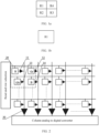
FIG. 1a and FIG. 1b are respectively schematic diagrams of pixels included in a pixel group according to an exemplary embodiment of this application; -
FIG. 2 is a schematic diagram of a structure of an image sensor according to an exemplary embodiment of this application; and -
FIG. 3 is an exploded schematic diagram of a camera module according to an exemplary embodiment of this application. - The embodiments of this application are described in detail below. Examples of the embodiments are shown in the accompanying drawings, and the same or similar reference signs indicate the same or similar components or components with the same or similar functions. The embodiments described below with reference to the drawings are exemplary and only used to explain this application, but cannot be understood as a limitation on this application. All other embodiments obtained by a person of ordinary skill in the art based on the embodiments of this application without creative efforts shall fall within the protection scope of this application.
- Features of the terms "first" and "second" in the specification and claims of this application may include one or more of the features explicitly or implicitly. In the descriptions of this application, unless otherwise stated, "a plurality of" means at least two. In addition, the term "and/or" in the specification and claims indicates at least one of connected objects, and the character "/" generally represents an "or" relationship between associated objects.
- In the descriptions of this application, it should be understood that orientations or positional relationships indicated by the terms "center", "vertical", "transverse", "length", "width", "thickness", "upper", "lower", "front", "rear", "left", "right", "perpendicular", "horizontal", "top", "bottom", "inside", "outside", "clockwise", "counterclockwise", "axial", " radial", "circumferential", and the like are based on orientations or positional relationships shown in the accompanying drawings, are merely intended to facilitate the descriptions of this application and simplify the descriptions, are not intended to indicate or imply that the apparatuses or components mentioned in this application must have specific orientations or be constructed and operated for a specific orientation, and therefore shall not be construed as a limitation on this application.
- In the descriptions of this application, it should be noted that unless otherwise specified and defined explicitly, the term "installation", "link", or "connection" should be understood in its broad sense. For example, the term may be a fixed connection, a detachable connection, or an integrated connection, or may be a mechanical connection or an electrical connection, or may be a direct connection, an indirect connection through an intermediate medium, or an internal connection between two components. A person of ordinary skill in the art can understand specific meanings of the terms in this application based on specific situations.
- An exemplary embodiment of this application provides an image sensor. The image sensor is a semiconductor that may be configured to record light changes. The image sensor may be a complementary metal oxide semiconductor (Complementary Metal Oxide Semiconductor, CMOS) image sensor, a charge coupled device (Charge Coupled Device, CCD) image sensor, a quantum film image sensor, or the like.
- In this embodiment, the image sensor may include a pixel array and amplifiers, where the pixel array includes a plurality of pixel groups (for example, at least two pixel groups) arranged in a row direction and/or a column direction, each pixel group may include a plurality of pixels of different colors, such as a red photosensitive pixel, a green photosensitive pixel, and a blue photosensitive pixel, and each amplifier is in a one-to-one correspondence with each pixel.
- An input end of a target amplifier is connected to an output end of a target pixel, an output end of the target amplifier is connected to a column line in which the target pixel is located, the target amplifier is any one of the plurality of amplifiers, and the target pixel is a pixel corresponding to the target amplifier. Therefore, a pixel channel corresponding to the target pixel can be controlled separately, and each pixel channel can be amplified independently, so that the image sensor can have a function for implementing image processing (such as brightness uniformity (lens shading) processing). In other words, in this application, an amplifier is added in the image sensor, so that an image amplification operation in an ISP can be implemented in the front-end image sensor, to reduce noise components at the front end, suppress image noise, improve final image quality, increase a signal-to-noise ratio, and improve user experience.
- In this embodiment, the target pixel may be but is not limited to a red photosensitive pixel, a blue photosensitive pixel, a green photosensitive pixel, or the like. It may be understood that a pixel of a different color included in each pixel group may include at least one sub-pixel. For example, assuming that the pixel group includes a red photosensitive pixel, a green photosensitive pixel, and a blue photosensitive pixel, and using the red photosensitive pixel as an example herein, the red photosensitive pixel may include a total of four red photosensitive sub-pixels R1, R2, R3, and R4 shown in
FIG. 1a , or may include only one red photosensitive pixel R1 shown inFIG. 1b . This is not limited herein in this embodiment. In addition, in the pixel array, arrangements of the pixels of different colors in each pixel group may be the same or different. - Further, the amplifier may be but is not limited to an operational amplifier or the like. A gain (gain) of the amplifier may be set based on an actual requirement. For example, when a shooting environment changes, image quality can be ensured by adjusting the gain of the amplifier, that is, the gain of the amplifier is adjustable.
- In an implementation, based on different requirements for a gain of each pixel channel, only an output of a target pixel (such as a red photosensitive pixel, a blue photosensitive pixel, or a green photosensitive pixel) in a row in the pixel array may be amplified by using one amplifier, or outputs of target pixels in a plurality of rows in the pixel array may be separately amplified by using a plurality of amplifiers, or outputs of a plurality of target pixels of different colors may be simultaneously amplified by using a plurality of amplifiers corresponding to the pixels of different colors. This is not limited in this embodiment.
- On a basis of the foregoing embodiment, in a possible implementation, each pixel group may include a first pixel, a second pixel, and a third pixel, and correspondingly, the amplifiers may include a first amplifier, a second amplifier, and a third amplifier.
- An input end of the first amplifier is connected to an output end of the first pixel, and an output end of the first amplifier is connected to a column line in which the first pixel is located; an input end of the second amplifier is connected to an output end of the second pixel, and an output end of the second amplifier is connected to a column line in which the second pixel is located; and an input end of the third amplifier is connected to an output end of the third pixel, and an output end of the third amplifier is connected to a column line in which the third pixel is located. Because amplifiers corresponding to different pixels are added in the image sensor to amplify outputs of different pixel channels, the image sensor has a function for controlling each pixel channel separately, thereby implementing image processing functions such as image brightness uniformity processing, improving the final image quality, increasing the signal-to-noise ratio, and improving user experience. It may be understood that in this implementation, the first pixel, the second pixel, and the third pixel are the corresponding red photosensitive pixel, green photosensitive pixel, and blue photosensitive pixel respectively, that is, the pixel group including the first pixel, the second pixel, and the third pixel is a three-channel pixel group.
- In another possible implementation, each pixel group may include a first pixel, a second pixel, and a third pixel, and the second pixel includes a first sub-pixel and a second sub-pixel; and correspondingly, the amplifiers may include a first amplifier, a second amplifier, and a third amplifier, and the second amplifier includes a first sub-amplifier and a second sub-amplifier.
- An input end of the first amplifier is connected to an output end of the first pixel, and an output end of the first amplifier is connected to a column line in which the first pixel is located; an input end of the first sub-amplifier is connected to an output end of the first sub-pixel, and an output end of the first sub-amplifier is connected to a column line in which the first sub-pixel is located; an input end of the second sub-amplifier is connected to an output end of the second sub-pixel, and an output end of the second sub-amplifier is connected to a column line in which the second sub-pixel is located; and an input end of the third amplifier is connected to an output end of the third pixel, and an output end of the third amplifier is connected to a column line in which the third pixel is located. It may be understood that in this implementation, the first pixel and the third pixel correspond to the red photosensitive pixel and blue photosensitive pixel, and that both the first sub-pixel and the second sub-pixel correspond to the green photosensitive pixel, that is, the pixel group including the first pixel, the first sub-pixel, the second sub-pixel, and the third pixel is a four-channel pixel group.
- For example, referring to
FIG. 2 , a four-channel pixel group is used as an example herein to describe a connection mode of an amplifier in the image sensor. It is assumed that a first pixel included in apixel group 20 is a red photosensitive pixel (R), and that first sub-pixel and second sub-pixel are both green photosensitive pixels (Gr and Gb), and that a third pixel is a blue photosensitive pixel (B). In this case, an output of the R pixel is connected to the input end of thefirst amplifier 11, and the output is amplified by the first amplifier and then connected back to a column line in which the R pixel is located; an output of the Gr pixel is connected to the input end of thefirst sub-amplifier 12, and the output is amplified by the first sub-amplifier and then connected back to a column line in which the Gr pixel is located; an output of the Gb pixel is connected to the input end of thesecond sub-amplifier 13, and the output is amplified by the second sub-amplifier and then connected back to a column line in which the Gb pixel is located; an output of the B pixel is connected to the input end of thethird amplifier 14, and the output is amplified by the third amplifier and then connected back to a column line in which the B pixel is located; and finally, acolumn amplifier 30 completes subsequent column amplification (column amplification means amplifying all signals in the image sensor; this column amplifier can only amplify all the signals as a whole, but cannot amplify a channel separately), and an analog to digital converter (ADC) completes conversion. In this case, the first amplifier, the first sub-amplifier, the second sub-amplifier, and the third amplifier respectively control pixel channels corresponding to different colors, so that the image sensor has image processing functions such as brightness uniformity processing. - Gains of the first amplifier, the second amplifier (or the first sub-amplifier and the second sub-amplifier), and the third amplifier may be set based on an actual requirement. Details are hereinafter described with reference to different examples.
- Example 1: Considering that when the ISP passes through a lens shading module, image brightness becomes increasingly dark from the center to four corners due to characteristics of lens shading, in this embodiment, a brightness gain matrix needed to compensate for lens shading is calculated, and then the brightness gain matrix is mapped to each amplifier to implement a lens shading compensation function at the image sensor. In other words, in this embodiment, a gain of each amplifier may be determined based on the brightness gain matrix. The brightness gain matrix is obtained, by using the image processor (ISP), by calculating brightness uniformity of a raw image output by the image sensor. Therefore, the lens shading compensation function of the image sensor can be implemented, to reduce noise components at the front end, avoid lens shading compensation processing at the ISP, suppress image noise, improve the final image quality, increase the signal-to-noise ratio, and improve user experience.
- In an implementation, the foregoing implementation process may include: first, obtaining a first raw image by using the image sensor; then inputting the first raw image into the ISP, and processing the first raw image by using a brightness uniformity algorithm, to obtain a brightness gain matrix; then setting the brightness gain matrix as the gain of each amplifier in the image sensor; and finally, obtaining a second raw image by using the image sensor again. In this case, the second raw image is an image on which brightness uniformity processing has been performed, that is, an automatic brightness uniformity processing function of the image sensor is implemented. When the environment changes, the foregoing steps can be repeated to complete dynamic refreshing of the brightness uniformity processing of the image sensor.
- Example 2: If both the first sub-pixel and the second sub-pixel are green photosensitive pixels (such as Gr and Gb), a gain of the first sub-amplifier is different from a gain of the second sub-amplifier. For example, if a Gr channel and a Gb channel are processed by using different gains, a dynamic range of the image sensor can be improved, although a resolution of the image sensor is sacrificed. It may be understood that if signals of the Gr channel and the Gb channel in the image sensor are closer, the resolution of the image sensor is higher, and image quality of an image signal output by the image sensor is better.
- That a gain of the first sub-amplifier is different from a gain of the second sub-amplifier may include that there is a multiple relationship (multiple difference) between the gain of the first sub-amplifier and the gain of the second sub-amplifier. For example, the gain of the first sub-amplifier and the gain of the second sub-amplifier corresponding to the Gr channel and the Gb channel may be set to an integer multiple difference, such as 2x, 3x, or 4x. This is not limited herein. Therefore, the dynamic range of the image sensor is effectively improved.
- It should be noted that the multiple relationship may be determined based on a target shooting scene, where the target shooting scene includes a portrait shooting scene and/or a sky shooting scene or the like. This is not limited in this embodiment.
- For example, a face sky scene is used as an example herein. When a user takes selfies with a front camera on a smart product such as a mobile phone, the user often encounters a face sky scene. Generally, a 1x gain is required for the Gb channel to ensure normal exposure of the sky, but a face is underexposed. In this case, the Gr channel and the Gb channel can support processing with different gains, for example, the sky (that is, the sky scene) is processed by using a 1x gain (1x gain) of the Gr channel, while the face can be processed by using a 4x gain (4x gain) of the Gb channel, that is, there is a 4x relationship between the gain of the first sub-amplifier and the gain of the second sub-amplifier. Therefore, both the sky and the face can be in a normal exposure state, quality of the image output by the image sensor can be improved, and user experience is ensured.
- It should be noted that in the foregoing implementations, gains of a plurality of target amplifiers are the same or different, where the plurality of target amplifiers correspond to pixels of a same color, and the target amplifier may be the first amplifier, the second amplifier (including the first sub-amplifier or the second sub-amplifier), or the third amplifier. For example, using the first amplifier as an example, gains of a plurality of first amplifiers may be the same or different, and may be set based on an actual requirement. This is not limited in this embodiment.
- On a basis of the image sensor provided in the foregoing implementations, in a possible implementation, the image sensor may further include a micro-lens (Micro-lens) and a color filter (color filter). The micro-lens (micro-lens) is configured to focus light on each photodiode in a light pixel array. The color filter is configured to filter incident light, only allowing light of a waveband corresponding to a color of the color filter to pass. When illuminated, the photodiode generates an electrical charge and converts the light into an electrical signal.
- Further, an exemplary embodiment of this application further provides a camera module. The camera module includes the image sensor provided in the foregoing embodiment, and a lens group in the camera module is disposed in a correspondence with the image sensor, so that light passing through the lens group arrives at the image sensor. It may be understood that because the image sensor included in this embodiment has technical features the same as or similar to those of the image sensor provided in the foregoing embodiment, details are not described herein again to avoid repetition.
- For example, as shown in
FIG. 3 , the camera module may further include aprotective film 201, a lens (Lens) 202, a voice coil motor (Voice Coil Motor) 203, a supportingpart 204, an infrared filter (IR Filter) 205, animage sensor 206 provided in this application, a flexible board (FPC) 207, and a connectingpart 208. - A working process of the camera module may include the following (1) to (4).
- (1) The lens is used for light concentration and focusing. The lens is wrapped and fixed by the voice coil motor, and upper and lower ends of the voice coil motor are linked to a spring. During focusing, the motor is energized to generate electromagnetic force, and the electromagnetic force is finally balanced with elastic force of the spring. A location of the motor may be controlled by a magnitude of energization, and further, the lens is pushed to an in-focus position by the motor.
- The voice coil motor includes an upper cover, an upper spring, a lower spring, a housing, a coil, a magnet, a moving part, a base, and a terminal. The upper cover has a protection function for a motor. When deformed, the upper spring generates acting force on the motor to balance the electromagnetic force with the lower spring. The housing is a main frame of a fixed part of the motor, has a magnetic conduction function, and can improve effective utilization of the magnet. When the coil is energized, the coil generates upward thrust under action of a magnetic field of the magnet, to drive other parts of the moving part to move together. The magnet generates the magnetic field, so that the energized coil generates the electromagnetic force under the action of the magnetic field, allowing the moving part to move with the lens. When deformed, the lower spring generates acting force on the motor to balance the electromagnetic force with the upper spring. The base and the motor are directly assembled with the flexible board. A mobile phone supplies power to the motor by using the terminal.
- (2) The
image sensor 206 senses light. - Light is projected from an object to a color filter (IR filter) in the
image sensor 206, and the IR filter filters out undesired light to prevent theimage sensor 206 from generating false colors or ripples, and improve an effective resolution and color reproducibility of the image sensor. The light passing through the IR filter can be sensed by theimage sensor 206. - After sensing the light, the
image sensor 206 converts an optical signal into an electrical signal. The electrical signal is amplified and converted into a digital signal by an ADC, and a raw image is formed and output to an image processor ISP - (3) The image is processed and fed back to the sensor for processing.
- The raw image obtained in (2) is processed by ISP algorithm modules such as auto exposure (AE), auto focus (AF), AWB, OB, and lens shading, and a brightness gain matrix required for correct brightness uniformity processing is obtained. Then the brightness gain matrix is set as amplification gains (that is, gains) of an R channel (corresponding to a first amplifier), a Gr channel (corresponding to a first sub-amplifier), a Gb channel (corresponding to a second sub-amplifier), and a B channel (corresponding to a third amplifier) on the
image sensor 206, that is, a brightness uniformity processing function setting of theimage sensor 206 is completed. When an environment changes, the foregoing steps can be repeated to complete dynamic refreshing of the brightness uniformity processing of theimage sensor 206. - In addition, if the gains of the Gr channel (corresponding to the first sub-amplifier) and the Gb channel (corresponding to the second sub-amplifier) are set to a multiple difference, a dynamic range of the sensor can also be improved.
- (4) The image is processed and compressed for storage.
- The raw image output by the
image sensor 206 enters the ISP for processing, and is compressed into a JPEG image for storage or sending to a display after sharpening, noise reduction, color calibration, and other operations. - An exemplary embodiment of this application further provides an electronic device. The electronic device includes the
image sensor 206 provided in the foregoing embodiment. Because theimage sensor 206 included in this embodiment has technical features the same as or similar to those of theimage sensor 206 provided in the foregoing embodiments, details are not described herein again to avoid repetition. - In the description of this specification, the description referring to the terms "an embodiment", "some embodiments", "an exemplary embodiment", "an example", "a specific example", or "some examples" means that a specific feature, structure, material, or characteristic described with reference to the embodiment or example is included in at least one embodiment or example of this application. In this specification, illustrative expressions of the terms do not necessarily refer to the same embodiment or example. Moreover, the specific feature, structure, material, or characteristic described may be combined in any suitable manner in any one or more embodiments or examples.
- Although the embodiments of this application have been shown and described, a person of ordinary skill in the art can understand that various changes, modifications, substitutions, and variations of these embodiments may be made without departing from the principles and objectives of this application. The scope of this application is defined by the claims and their equivalents.
Claims (11)
- An image sensor, comprising a pixel array and a plurality of amplifiers, wherein the pixel array comprises a plurality of pixel groups arranged in a row direction and/or a column direction, each pixel group comprises a plurality of pixels of different colors, and each amplifier is in a one-to-one correspondence with each pixel, wherein
an input end of a target amplifier is connected to an output end of a target pixel, an output end of the target amplifier is connected to a column line in which the target pixel is located, the target amplifier is any one of the plurality of amplifiers, and the target pixel is a pixel corresponding to the target amplifier. - The image sensor according to claim 1, wherein the plurality of amplifiers comprise a first amplifier, a second amplifier, and a third amplifier, and each pixel group comprises a first pixel, a second pixel, and a third pixel;an input end of the first amplifier is connected to an output end of the first pixel, and an output end of the first amplifier is connected to a column line in which the first pixel is located;an input end of the second amplifier is connected to an output end of the second pixel, and an output end of the second amplifier is connected to a column line in which the second pixel is located; andan input end of the third amplifier is connected to an output end of the third pixel, and an output end of the third amplifier is connected to a column line in which the third pixel is located.
- The image sensor according to claim 2, wherein the second pixel comprises a first sub-pixel and a second sub-pixel, and the second amplifier comprises a first sub-amplifier and a second sub-amplifier;an input end of the first sub-amplifier is connected to an output end of the first sub-pixel, and an output end of the first sub-amplifier is connected to a column line in which the first sub-pixel is located; andan input end of the second sub-amplifier is connected to an output end of the second sub-pixel, and an output end of the second sub-amplifier is connected to a column line in which the second sub-pixel is located.
- The image sensor according to claim 3, wherein the first sub-pixel and the second sub-pixel are both green photosensitive pixels, and a gain of the first sub-amplifier is different from a gain of the second sub-amplifier.
- The image sensor according to claim 4, wherein that a gain of the first sub-amplifier is different from a gain of the second sub-amplifier comprises that there is a multiple relationship between the gain of the first sub-amplifier and the gain of the second sub-amplifier.
- The image sensor according to claim 5, wherein the multiple relationship is determined based on a target shooting scene, and the target shooting scene comprises a portrait shooting scene and/or a sky shooting scene.
- The image sensor according to any one of claims 1 to 3, wherein a plurality of target amplifiers have a same gain, and the plurality of target amplifiers correspond to pixels of a same color.
- The image sensor according to any one of claims 1 to 3, wherein a gain of each amplifier is determined based on a brightness gain matrix, and the brightness gain matrix is obtained, by using an image processor ISP, by calculating brightness uniformity of a raw image output by the image sensor.
- The image sensor according to any one of claims 1 to 3, wherein the gain of each amplifier is adjustable.
- A camera module, comprising the image sensor according to any one of claims 1 to 9, wherein a lens group in the camera module is disposed in a correspondence with the image sensor.
- An electronic device, wherein the electronic device comprises the image sensor according to any one of claims 1 to 9.
Applications Claiming Priority (2)
| Application Number | Priority Date | Filing Date | Title |
|---|---|---|---|
| CN202011373308.2A CN112492162B (en) | 2020-11-30 | 2020-11-30 | Image sensor, camera module and electronic equipment |
| PCT/CN2021/132700 WO2022111508A1 (en) | 2020-11-30 | 2021-11-24 | Image sensor, camera module and electronic device |
Publications (3)
| Publication Number | Publication Date |
|---|---|
| EP4254930A1 true EP4254930A1 (en) | 2023-10-04 |
| EP4254930A4 EP4254930A4 (en) | 2024-02-07 |
| EP4254930B1 EP4254930B1 (en) | 2026-03-18 |
Family
ID=74937361
Family Applications (1)
| Application Number | Title | Priority Date | Filing Date |
|---|---|---|---|
| EP21897009.3A Active EP4254930B1 (en) | 2020-11-30 | 2021-11-24 | Image sensor, camera module and electronic device |
Country Status (5)
| Country | Link |
|---|---|
| US (1) | US12513426B2 (en) |
| EP (1) | EP4254930B1 (en) |
| JP (1) | JP7661492B2 (en) |
| CN (1) | CN112492162B (en) |
| WO (1) | WO2022111508A1 (en) |
Families Citing this family (1)
| Publication number | Priority date | Publication date | Assignee | Title |
|---|---|---|---|---|
| CN112492162B (en) * | 2020-11-30 | 2022-04-01 | 维沃移动通信有限公司 | Image sensor, camera module and electronic equipment |
Family Cites Families (29)
| Publication number | Priority date | Publication date | Assignee | Title |
|---|---|---|---|---|
| DE19652477A1 (en) * | 1996-12-17 | 1998-06-18 | Wolf Henning | Electronic camera with controllable pixels |
| JP4327928B2 (en) * | 1999-02-26 | 2009-09-09 | メディア・テック・ユーエスエイ・インコーポレーテッド | Electronic camera device |
| JP4284754B2 (en) * | 1999-05-31 | 2009-06-24 | ソニー株式会社 | Color imaging apparatus and control method thereof |
| US6339363B1 (en) * | 2000-12-04 | 2002-01-15 | Pixel Devices International | Low FPN high gain capacitive transimpedance amplifier for use with capacitive sensors |
| US7616231B2 (en) * | 2005-01-06 | 2009-11-10 | Goodrich Corporation | CMOS active pixel sensor with improved dynamic range and method of operation for object motion detection |
| US7518645B2 (en) * | 2005-01-06 | 2009-04-14 | Goodrich Corp. | CMOS active pixel sensor with improved dynamic range and method of operation |
| US7636115B2 (en) * | 2005-08-11 | 2009-12-22 | Aptina Imaging Corporation | High dynamic range imaging device using multiple pixel cells |
| JP2009225315A (en) | 2008-03-18 | 2009-10-01 | Canon Inc | Imaging apparatus |
| JP5165520B2 (en) * | 2008-10-01 | 2013-03-21 | ソニー株式会社 | Solid-state imaging device, imaging device, and AD conversion method for solid-state imaging device |
| CN101521755A (en) * | 2008-12-15 | 2009-09-02 | 昆山锐芯微电子有限公司 | Cmos image sensor reading circuit and reading method |
| JP2010278603A (en) | 2009-05-27 | 2010-12-09 | Kyocera Corp | Imaging module |
| JP4764950B2 (en) | 2010-07-06 | 2011-09-07 | キヤノン株式会社 | Imaging device |
| WO2012081154A1 (en) | 2010-12-16 | 2012-06-21 | パナソニック株式会社 | Imaging device and image processing device |
| US8896733B2 (en) * | 2011-01-21 | 2014-11-25 | Aptina Imaging Corporation | Imaging system with automatic conversion gain selection |
| JP2012227590A (en) | 2011-04-15 | 2012-11-15 | Canon Inc | Solid state imaging element and imaging apparatus |
| JP5519083B2 (en) * | 2011-09-29 | 2014-06-11 | 富士フイルム株式会社 | Image processing apparatus, method, program, and imaging apparatus |
| JP6041531B2 (en) * | 2012-05-24 | 2016-12-07 | キヤノン株式会社 | Photoelectric conversion device |
| US9106851B2 (en) | 2013-03-12 | 2015-08-11 | Tower Semiconductor Ltd. | Single-exposure high dynamic range CMOS image sensor pixel with internal charge amplifier |
| US8902343B1 (en) * | 2013-06-25 | 2014-12-02 | Altasens, Inc. | Charge pump for pixel floating diffusion gain control |
| US9571763B2 (en) * | 2014-01-10 | 2017-02-14 | Omnivision Technologies, Inc. | Split pixel high dynamic range sensor |
| JP6478600B2 (en) * | 2014-12-04 | 2019-03-06 | キヤノン株式会社 | Imaging apparatus and control method thereof |
| US9947712B2 (en) | 2016-01-27 | 2018-04-17 | Varex Imaging Corporation | Matrix type integrated circuit with fault isolation capability |
| CN106101589A (en) * | 2016-07-15 | 2016-11-09 | 王海英 | A high dynamic BiCMOS image sensor and its pixel unit |
| CN106412407B (en) | 2016-11-29 | 2019-06-07 | Oppo广东移动通信有限公司 | Control method, control device and electronic device |
| KR102678455B1 (en) | 2016-12-30 | 2024-06-27 | 삼성전자주식회사 | Image sensor |
| KR102333610B1 (en) | 2017-03-06 | 2021-12-03 | 에스케이하이닉스 주식회사 | Image sensor |
| FR3074991B1 (en) * | 2017-12-07 | 2019-11-22 | Teledyne E2V Semiconductors Sas | HIGH DYNAMIC IMAGE SENSOR |
| JP7077029B2 (en) * | 2018-01-26 | 2022-05-30 | キヤノン株式会社 | Photoelectric converter, imaging system, moving object |
| CN112492162B (en) * | 2020-11-30 | 2022-04-01 | 维沃移动通信有限公司 | Image sensor, camera module and electronic equipment |
-
2020
- 2020-11-30 CN CN202011373308.2A patent/CN112492162B/en active Active
-
2021
- 2021-11-24 WO PCT/CN2021/132700 patent/WO2022111508A1/en not_active Ceased
- 2021-11-24 EP EP21897009.3A patent/EP4254930B1/en active Active
- 2021-11-24 JP JP2023532577A patent/JP7661492B2/en active Active
-
2023
- 2023-05-25 US US18/323,656 patent/US12513426B2/en active Active
Also Published As
| Publication number | Publication date |
|---|---|
| CN112492162B (en) | 2022-04-01 |
| KR20230107877A (en) | 2023-07-18 |
| US12513426B2 (en) | 2025-12-30 |
| CN112492162A (en) | 2021-03-12 |
| US20230300491A1 (en) | 2023-09-21 |
| EP4254930A4 (en) | 2024-02-07 |
| EP4254930B1 (en) | 2026-03-18 |
| WO2022111508A1 (en) | 2022-06-02 |
| JP2023551038A (en) | 2023-12-06 |
| JP7661492B2 (en) | 2025-04-14 |
Similar Documents
| Publication | Publication Date | Title |
|---|---|---|
| US8174595B2 (en) | Drive unit for image sensor, and drive method for imaging device | |
| US9549166B2 (en) | Imaging device and shading correction method | |
| JP5946421B2 (en) | Imaging apparatus and control method thereof | |
| US9179077B2 (en) | Array camera imaging system and method | |
| KR20080056018A (en) | Ambient Light Correction Device, Ambient Light Correction Method, Electronic Information Equipment, Control Program, and Readable Recording Media | |
| US12244949B2 (en) | Image sensor and imaging device with vertical controller performing first control and second control | |
| US10425605B2 (en) | Image sensor and image capturing apparatus | |
| US20130050543A1 (en) | Image pickup unit and image processing unit | |
| CN114679551B (en) | Solid-state imaging device, signal processing method for solid-state imaging device, and electronic apparatus | |
| US20140104470A1 (en) | Data transfer circuit, imaging device and imaginapparatus | |
| EP3813364A1 (en) | Image device | |
| US12513426B2 (en) | Image sensor, camera module, and electronic device | |
| US7595821B2 (en) | Solid-state image pickup device and camera using the same | |
| US10871629B2 (en) | Imaging apparatus and control method of imaging apparatus | |
| US20090027514A1 (en) | Image pickup apparatus and method | |
| JP2020123762A (en) | Imaging device and imaging device | |
| US20250211877A1 (en) | Image capturing apparatus, control method of image sensor, and electronic apparatus | |
| JP2008113236A (en) | Shading correction method and apparatus in imaging apparatus | |
| JP2020092346A (en) | Imaging device and method of controlling the same | |
| JP2005109993A (en) | Imaging device | |
| CN112492161B (en) | Image sensor, camera module and electronic equipment | |
| JP2016134857A (en) | Imaging device and control method therefor, program, storage medium | |
| KR102965578B1 (en) | Image sensors, camera modules, and electronic devices | |
| US20030220741A1 (en) | Signal processing apparatus and signal processing program | |
| JP2018005161A (en) | Control device, image capturing device, control method, program, and storage medium |
Legal Events
| Date | Code | Title | Description |
|---|---|---|---|
| STAA | Information on the status of an ep patent application or granted ep patent |
Free format text: STATUS: THE INTERNATIONAL PUBLICATION HAS BEEN MADE |
|
| PUAI | Public reference made under article 153(3) epc to a published international application that has entered the european phase |
Free format text: ORIGINAL CODE: 0009012 |
|
| STAA | Information on the status of an ep patent application or granted ep patent |
Free format text: STATUS: REQUEST FOR EXAMINATION WAS MADE |
|
| 17P | Request for examination filed |
Effective date: 20230621 |
|
| AK | Designated contracting states |
Kind code of ref document: A1 Designated state(s): AL AT BE BG CH CY CZ DE DK EE ES FI FR GB GR HR HU IE IS IT LI LT LU LV MC MK MT NL NO PL PT RO RS SE SI SK SM TR |
|
| REG | Reference to a national code |
Ref country code: DE Free format text: PREVIOUS MAIN CLASS: H04N0005225000 Ref legal event code: R079 Ref document number: 602021050379 Country of ref document: DE Ipc: H04N0025770000 |
|
| A4 | Supplementary search report drawn up and despatched |
Effective date: 20240108 |
|
| RIC1 | Information provided on ipc code assigned before grant |
Ipc: H04N 23/57 20230101ALN20240102BHEP Ipc: H04N 25/61 20230101ALN20240102BHEP Ipc: H04N 25/57 20230101ALN20240102BHEP Ipc: H04N 25/78 20230101ALI20240102BHEP Ipc: H04N 25/51 20230101ALI20240102BHEP Ipc: H04N 25/77 20230101AFI20240102BHEP |
|
| DAV | Request for validation of the european patent (deleted) | ||
| DAX | Request for extension of the european patent (deleted) | ||
| STAA | Information on the status of an ep patent application or granted ep patent |
Free format text: STATUS: EXAMINATION IS IN PROGRESS |
|
| 17Q | First examination report despatched |
Effective date: 20250423 |
|
| RIC1 | Information provided on ipc code assigned before grant |
Ipc: H04N 25/77 20230101AFI20251205BHEP Ipc: H04N 25/51 20230101ALI20251205BHEP Ipc: H04N 25/78 20230101ALI20251205BHEP Ipc: H04N 23/611 20230101ALI20251205BHEP Ipc: H04N 23/76 20230101ALI20251205BHEP Ipc: H04N 25/57 20230101ALN20251205BHEP Ipc: H04N 25/61 20230101ALN20251205BHEP Ipc: H04N 23/57 20230101ALN20251205BHEP |
|
| GRAP | Despatch of communication of intention to grant a patent |
Free format text: ORIGINAL CODE: EPIDOSNIGR1 |
|
| STAA | Information on the status of an ep patent application or granted ep patent |
Free format text: STATUS: GRANT OF PATENT IS INTENDED |
|
| RIC1 | Information provided on ipc code assigned before grant |
Ipc: H04N 25/77 20230101AFI20251222BHEP Ipc: H04N 25/51 20230101ALI20251222BHEP Ipc: H04N 25/78 20230101ALI20251222BHEP Ipc: H04N 23/611 20230101ALI20251222BHEP Ipc: H04N 23/76 20230101ALI20251222BHEP Ipc: H04N 25/57 20230101ALN20251222BHEP Ipc: H04N 25/61 20230101ALN20251222BHEP Ipc: H04N 23/57 20230101ALN20251222BHEP |
|
| GRAS | Grant fee paid |
Free format text: ORIGINAL CODE: EPIDOSNIGR3 |
|
| GRAA | (expected) grant |
Free format text: ORIGINAL CODE: 0009210 |
|
| STAA | Information on the status of an ep patent application or granted ep patent |
Free format text: STATUS: THE PATENT HAS BEEN GRANTED |
|
| INTG | Intention to grant announced |
Effective date: 20260121 |
|
| AK | Designated contracting states |
Kind code of ref document: B1 Designated state(s): AL AT BE BG CH CY CZ DE DK EE ES FI FR GB GR HR HU IE IS IT LI LT LU LV MC MK MT NL NO PL PT RO RS SE SI SK SM TR |
|
| REG | Reference to a national code |
Ref country code: CH Ref legal event code: F10 Free format text: ST27 STATUS EVENT CODE: U-0-0-F10-F00 (AS PROVIDED BY THE NATIONAL OFFICE) Effective date: 20260318 Ref country code: GB Ref legal event code: FG4D |
|
| REG | Reference to a national code |
Ref country code: IE Ref legal event code: FG4D |
|
| REG | Reference to a national code |
Ref country code: DE Ref legal event code: R096 Ref document number: 602021050379 Country of ref document: DE |