EP4254685A1 - Rotating connector device - Google Patents
Rotating connector device Download PDFInfo
- Publication number
- EP4254685A1 EP4254685A1 EP21906258.5A EP21906258A EP4254685A1 EP 4254685 A1 EP4254685 A1 EP 4254685A1 EP 21906258 A EP21906258 A EP 21906258A EP 4254685 A1 EP4254685 A1 EP 4254685A1
- Authority
- EP
- European Patent Office
- Prior art keywords
- flat cable
- conductors
- rotating
- flat
- connector device
- Prior art date
- Legal status (The legal status is an assumption and is not a legal conclusion. Google has not performed a legal analysis and makes no representation as to the accuracy of the status listed.)
- Granted
Links
Images




Classifications
-
- H—ELECTRICITY
- H01—ELECTRIC ELEMENTS
- H01R—ELECTRICALLY-CONDUCTIVE CONNECTIONS; STRUCTURAL ASSOCIATIONS OF A PLURALITY OF MUTUALLY-INSULATED ELECTRICAL CONNECTING ELEMENTS; COUPLING DEVICES; CURRENT COLLECTORS
- H01R35/00—Flexible or turnable line connectors, i.e. the rotation angle being limited
- H01R35/02—Flexible line connectors without frictional contact members
- H01R35/025—Flexible line connectors without frictional contact members having a flexible conductor wound around a rotation axis
-
- H—ELECTRICITY
- H01—ELECTRIC ELEMENTS
- H01R—ELECTRICALLY-CONDUCTIVE CONNECTIONS; STRUCTURAL ASSOCIATIONS OF A PLURALITY OF MUTUALLY-INSULATED ELECTRICAL CONNECTING ELEMENTS; COUPLING DEVICES; CURRENT COLLECTORS
- H01R35/00—Flexible or turnable line connectors, i.e. the rotation angle being limited
- H01R35/04—Turnable line connectors with limited rotation angle with frictional contact members
-
- B—PERFORMING OPERATIONS; TRANSPORTING
- B60—VEHICLES IN GENERAL
- B60R—VEHICLES, VEHICLE FITTINGS, OR VEHICLE PARTS, NOT OTHERWISE PROVIDED FOR
- B60R16/00—Electric or fluid circuits specially adapted for vehicles and not otherwise provided for; Arrangement of elements of electric or fluid circuits specially adapted for vehicles and not otherwise provided for
- B60R16/02—Electric or fluid circuits specially adapted for vehicles and not otherwise provided for; Arrangement of elements of electric or fluid circuits specially adapted for vehicles and not otherwise provided for electric constitutive elements
- B60R16/023—Electric or fluid circuits specially adapted for vehicles and not otherwise provided for; Arrangement of elements of electric or fluid circuits specially adapted for vehicles and not otherwise provided for electric constitutive elements for transmission of signals between vehicle parts or subsystems
- B60R16/027—Electric or fluid circuits specially adapted for vehicles and not otherwise provided for; Arrangement of elements of electric or fluid circuits specially adapted for vehicles and not otherwise provided for electric constitutive elements for transmission of signals between vehicle parts or subsystems between relatively movable parts of the vehicle, e.g. between steering wheel and column
-
- H—ELECTRICITY
- H01—ELECTRIC ELEMENTS
- H01B—CABLES; CONDUCTORS; INSULATORS; SELECTION OF MATERIALS FOR THEIR CONDUCTIVE, INSULATING OR DIELECTRIC PROPERTIES
- H01B7/00—Insulated conductors or cables characterised by their form
- H01B7/08—Flat or ribbon cables
- H01B7/0861—Flat or ribbon cables comprising one or more screens
-
- H—ELECTRICITY
- H05—ELECTRIC TECHNIQUES NOT OTHERWISE PROVIDED FOR
- H05K—PRINTED CIRCUITS; CASINGS OR CONSTRUCTIONAL DETAILS OF ELECTRIC APPARATUS; MANUFACTURE OF ASSEMBLAGES OF ELECTRICAL COMPONENTS
- H05K1/00—Printed circuits
- H05K1/02—Details
- H05K1/0213—Electrical arrangements not otherwise provided for
- H05K1/0216—Reduction of cross-talk, noise or electromagnetic interference
- H05K1/0218—Reduction of cross-talk, noise or electromagnetic interference by printed shielding conductors, ground planes or power plane
-
- H—ELECTRICITY
- H01—ELECTRIC ELEMENTS
- H01R—ELECTRICALLY-CONDUCTIVE CONNECTIONS; STRUCTURAL ASSOCIATIONS OF A PLURALITY OF MUTUALLY-INSULATED ELECTRICAL CONNECTING ELEMENTS; COUPLING DEVICES; CURRENT COLLECTORS
- H01R13/00—Details of coupling devices of the kinds covered by groups H01R12/70 or H01R24/00 - H01R33/00
- H01R13/646—Details of coupling devices of the kinds covered by groups H01R12/70 or H01R24/00 - H01R33/00 specially adapted for high-frequency, e.g. structures providing an impedance match or phase match
- H01R13/6473—Impedance matching
-
- H—ELECTRICITY
- H01—ELECTRIC ELEMENTS
- H01R—ELECTRICALLY-CONDUCTIVE CONNECTIONS; STRUCTURAL ASSOCIATIONS OF A PLURALITY OF MUTUALLY-INSULATED ELECTRICAL CONNECTING ELEMENTS; COUPLING DEVICES; CURRENT COLLECTORS
- H01R2201/00—Connectors or connections adapted for particular applications
- H01R2201/26—Connectors or connections adapted for particular applications for vehicles
-
- H—ELECTRICITY
- H05—ELECTRIC TECHNIQUES NOT OTHERWISE PROVIDED FOR
- H05K—PRINTED CIRCUITS; CASINGS OR CONSTRUCTIONAL DETAILS OF ELECTRIC APPARATUS; MANUFACTURE OF ASSEMBLAGES OF ELECTRICAL COMPONENTS
- H05K2201/00—Indexing scheme relating to printed circuits covered by H05K1/00
- H05K2201/07—Electric details
- H05K2201/0707—Shielding
- H05K2201/0723—Shielding provided by an inner layer of PCB
Definitions
- the present invention relates to a rotating connector device for use as a steering roll connector.
- a rotating connector device which is provided with a fixed-side member, a rotating-side member which is rotatable relative to the fixed-side member, and a plurality of flat cables which are each formed by covering conductors with an insulating material and which are accommodated in a stacked state in an annular accommodating space formed between the fixed-side member and the rotating-side member (for example, see Patent Document 1).
- the rotating connector device may have disadvantages such as a decrease in electromagnetic compatibility due to electromagnetic noise and destabilization of impedance of communication circuit conductors, and accordingly. Therefore, it is required for the rotating connector device to reduce the disadvantages.
- CAN controller area network
- Patent Document 1 PCT International Publication No. WO2014/017649
- the flat cables each having communication circuit conductors and dummy flat cables having no conductor are integrally formed so that each dummy flat cable is disposed between the adjacent flat cables having conductors, to thereby suppress a decrease in the electromagnetic compatibility due to electromagnetic noise and the destabilization of the impedance of the communication circuit conductors of the flat cables. Therefore, in the rotating connector device of Patent Document 1, the entirety of the plurality of flat cables has a large dimension in the thickness direction, which may cause an increase in the size of the device.
- An object of the present invention is to provide a rotating connector device capable of improving electromagnetic compatibility and stabilizing impedance, while suppressing an increase in size of the device.
- a rotating connector device comprises a fixed-side member, a rotating-side member which is rotatable relative to the fixed-side member, and a plurality of flat cables which are each formed by covering conductors with an insulating material and which are accommodated in a stacked state in an annular accommodating space formed between the fixed-side member and the rotating-side member, wherein a shield film is disposed between at least a flat cable including target conductors and a flat cable adjacent to the flat cable including the target conductors that are selected from the plurality of flat cables.
- the shield film is formed integrally with the flat cable including the target conductors.
- the shield film is disposed on a portion in a width direction of the flat cable including the target conductors, where at least the target conductors are located.
- the shield film is formed integrally with one surface of each of the plurality of flat cables.
- the shield film is formed by vapor deposition of silver on a resin film.
- a shield film makes it possible to stabilize impedance of target conductors even when the number of stacked layers of a plurality of flat cables changes in an accommodating space, which makes it possible to suppress an increase in size of a device, and to improve electromagnetic compatibility and stabilize impedance.
- FIGS. 1 to 5 illustrate the first embodiment of the present invention.
- FIG. 1 is a perspective view of a rotating connector device according to a first embodiment of the present invention
- FIG. 2 is a perspective view illustrating the interior of the rotating connector device
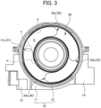
- FIG. 3 is a planar view illustrating the interior of the rotating connector device
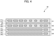
- FIG. 4 is a cross-sectional view illustrating first to fourth flat cables in FIG. 3
- FIG. 5 is a cross-sectional view illustrating the first flat cable.
- a rotating connector device 1 of the present embodiment is used as a so-called steering roll connector provided in a connecting portion between a steering column on a vehicle main body side and a steering shaft on a steering wheel side.
- the rotating connector device 1 forms a part of a communication circuit that transmits electrical signals between a main ECU provided on the vehicle main body side and a steering ECU provided on the steering wheel side and configured to control electric components disposed on the steering wheel side and that forms a part of other conductive circuits that transmit electric power and electrical signals between the vehicle main body side and the steering wheel side.
- the communication circuit performs high-speed communication of 100 Mbps or more, for example.
- the rotating connector device 1 is provided with a fixed-side housing 10 serving as a fixed-side member which is fixed to the steering column, a rotating-side housing 20 serving as a rotating-side member which is fixed to the steering shaft and which is rotatable relative to the fixed-side housing 10, and a plurality of flat cables 30 which are accommodated in an annular accommodating space S formed between the fixed-side housing 10 and the rotating-side housing 20.
- the fixed-side housing 10 includes a fixed-side ring part 11 in which an opening is provided so that the steering shaft can be inserted therethrough, and an outer circumferential cylindrical part 12 having a cylindrical shape and extending vertically from an outer circumferential side of the fixed-side ring part 11.
- An outer circumferential portion of the outer circumferential cylindrical part 12 is provided with a first fixed-side connector 13 to which one ends of some of the plurality of flat cables 30 are connected, and a second fixed-side connector 14 to which one ends of the other flat cables 30 are connected.
- the rotating-side housing 20 includes a rotating-side ring part 21 which is disposed to face the fixed-side ring part 11 and in which an opening is provided so that the steering shaft can be inserted therethrough, and an inner circumferential cylindrical part 22 which is disposed to face the outer circumferential cylindrical part 12, and extends vertically from an inter circumferential side of the rotating-side ring part 21.
- An outer surface of the rotating-side ring part 21 is provided with a first rotating-side connector 23 to which the other ends of some flat cables 30 whose one ends are connected to the first fixed-side connector 13 are connected, and a second rotating-side connector 24 to which the other ends of the other flat cables 30 whose one ends are connected to the second fixed-side connector 14 are connected.
- the accommodating space S is annularly formed by being defined by the fixed-side ring part 11 and the outer circumferential cylindrical part 12 in the fixed-side housing 10, and the rotating-side ring part 21 and the inner circumferential cylindrical part 22 in the rotating-side housing 20.
- the plurality of flat cables 30 are each formed into a belt shape having the same width directional dimension.
- the plurality of flat cables 30 are formed separately, and are accommodated in the accommodating space S in a detachably stacked state.
- the plurality of flat cables 30 have respective one ends fixed to the outer circumferential cylindrical part 12 and are wound along the inner circumferential surface of the outer circumferential cylindrical part 12 toward one side of a rotational direction of the rotating-side housing 20, and respective middle portions are reversed to form a U shape between the outer circumferential cylindrical part 12 and the inner circumferential cylindrical part 22 to be wound toward the other side of the rotational direction, and the respective other ends are fixed to the inner circumferential cylindrical part 22.
- the plurality of flat cables 30 comprise first to fourth flat cables 31, 32, 33, 34 (hereinafter, referred to as 31 to 34).
- the first to fourth flat cables 31 to 34 are formed into belt shapes by covering a plurality of conductors 31a, 32a, 33a, and 34a (hereinafter, referred to as 31a to 34a) disposed at intervals in the width direction with corresponding insulating materials 31b, 32b, 33b, and 34b (hereinafter, referred to as 31b to 34b).
- first to fourth flat cables 31 to 34 accommodated in the accommodating space S are detachably stacked on the radially outer side in order of the first flat cable 31, the second flat cable 32, the third flat cable 33, and the fourth flat cable 34 from the outer circumferential cylindrical part 12 side toward the inner circumferential cylindrical part 22 side.
- first to fourth flat cables 31 to 34 accommodated in the accommodating space S are detachably stacked on the radially inner side in order of the first flat cable 31, the second flat cable 32, the third flat cable 33, and the fourth flat cable 34 from the inner circumferential cylindrical part 22 side toward the outer circumferential cylindrical part 12 side. Furthermore, as illustrated in FIG.
- the respective middle portions are formed with U-turn portions 31c, 32c, 33c, and 34c (hereinafter, referred to as 31c to 34c) that move in association with the rotation of the rotating-side housing 20 relative to the fixed-side housing 10. Accordingly, in the case where the U-turn portions 31c to 34c are located at center portions in the longitudinal direction of the respective first to fourth flat cables 31 to 34, this allows the rotating-side housing 20 to rotate relative to the fixed-side housing 10 by the same angle in each of one direction and the other direction.
- a shield film 35 having a property of blocking and absorbing electromagnetic waves is disposed between, among the first to fourth flat cables 31 to 34, at least the first flat cable 31 including first and second communication circuit conductors (which will be described later) as target conductors and the second flat cable 32 adjacent to the first flat cable 31, to suppress the influence of the electromagnetic waves on the first and second communication circuit conductors.
- the first and second communication circuit conductors serving as the target conductors are conductors used as differential transmission lines.
- the shield film 35 may be disposed each between the plurality of flat cables 30. In the present embodiment, the shield film 35 is disposed only between the first flat cable 31 including the communication circuit conductors and the second flat cables 32.
- the shield film 35 disposed between the first flat cable 31 and the second flat cable 32 is formed integrally with any one of the first flat cable 31 and the second flat cable 32.
- the shield film 35 is formed integrally with the first flat cable 31.
- the first flat cable 31 includes, as a plurality of conductors 31a, first to fourth conductive circuit conductors 31a1, 31a2, 31a3, and 31a4 (hereinafter, referred to as 31a1 to 31a4), first and second communication circuit conductors 31a5 and 31a6, and first and second ground conductors 31a7 and 31a8. As illustrated in FIG.
- the first conductive circuit conductor 31a1, the first ground conductor 31a7, the first communication circuit conductor 31a5, the second communication circuit conductor 31a6, the second ground conductor 31a8, the second conductive circuit conductor 31a2, the third conductive circuit conductor 31a3, and the fourth conductive circuit conductor 31a4 are disposed at intervals in this order from the left end toward the right end in the width direction.
- the first flat cable 31 has a high-speed communication GSSG structure in which the first and second ground conductors 31a7 and 31a8 are disposed on the outer sides in the width direction of the first and second communication circuit conductors 31a5 and 31a6, respectively.
- the first to fourth conductive circuit conductors 31a1 to 31a4 are each formed into a rectangular cross-sectional shape having a width-directional dimension of 0.8 mm or more and a thickness-directional dimension of 35 ⁇ m.
- the first and second communication circuit conductors 31a5 and 31a6 and the first and second ground conductors 31a7 and 31a8 are each formed into a rectangular cross-sectional shape having a width-directional dimension of 0.1 mm and a thickness-directional dimension of 35 ⁇ m.
- the first and second communication circuit conductors 31a5 and 31a6 and the first and second ground conductors 31a7 and 31a8 are disposed so that each of a distance between the first ground conductor 31a7 and the first communication circuit conductor 31a5, a distance between the first communication circuit conductor 31a5 and the second communication circuit conductor 31a6, and a distance between the second communication circuit conductor 31a6 and the second ground conductor 31a8 is from 0.4 mm or more and 1 mm or less.
- the first insulating layer 31b1 includes a resin film 31b2 such as polyethylene terephthalate (PET) having a thickness dimension of 12 ⁇ m and an adhesive layer 31b3 having a thickness dimension of 20 ⁇ m.
- PET polyethylene terephthalate
- the second insulating layer 31b4 includes a resin film 31b5 having a thickness dimension of 25 ⁇ m and an adhesive layer 31b6 having a thickness dimension of 20 ⁇ m.
- the shield film 35 is disposed on an outer surface (a surface facing the second flat cable 32) of the second insulating layer 31b4 in the first flat cable 31.
- the shield film 35 includes a resin film 35a such as polyethylene terephthalate (PET) having a thickness dimension of 9 pm, a silver film 35b having a thickness dimension of 0.2 ⁇ m which is vapor-deposited on the resin film 35a, and an adhesive layer 35c having a thickness dimension of 20 um. It is only required that the silver film 35b is disposed in the same size as a gap between the first and second ground conductors 31a7 and 31a8 in the width direction of the first flat cable 31, and has a width dimension which makes it possible to cover the entirety of at least the first and second communication circuit conductors 31a5 and 31a6 from the second flat cable 32 side.
- PET polyethylene terephthalate
- the distance between the first and second communication circuit conductors 31a5 and 31a6, the distances between the first and second communication circuit conductors 31a5 and 31a6 and the first and second ground conductors 31a7 and 31a8, and the distance between the first and second communication circuit conductors 31a5 and 31a6 and the silver film 35b are set so that the impedance of the first and second communication circuit conductors 31a5 and 31a6 are within a range of from 90 Q to 110 Q.
- the plurality of flat cables 30 are accommodated in the accommodating space S in which the number of stacked layers of the flat cables 30 is different in each portion.
- the position in the rotational direction of the rotating-side housing 20 with respect to the fixed-side housing 10 is the middle position between an end on one direction side and an end on the other direction side
- the number of stacked layers is four in a portion a in FIG. 3 .
- a portion c in FIG. 3 is a U-turn portion 31c of the first flat cable 31, and the number of stacked layers is one.
- the number of stacked layers of the first to fourth flat cables 31 to 34 in the accommodating space S changes depending on the rotational position of the rotating-side housing 20 with respect to the fixed-side housing 10 at each portion. For example, in FIG. 3 , when the rotating-side housing 20 is rotated clockwise relative to the fixed-side housing 10, the number of stacked layers of the flat cables wound on the radially outer side changes in the increasing direction. The number of stacked layers of the flat cables wound on the radially inner side changes in the decreasing direction. Furthermore, a portion between one end and the other end of each of the first to fourth flat cables 31 to 34 where the number of stacked layers is one moves clockwise in the accommodating space S.
- the impedance of the first and second communication circuit conductors 31a5 and 31a6 in the first flat cable 31 changes with changes in inductance and capacitance.
- the second to fourth flat cables 32, 33, and 34 move toward and away from the first flat cable 31, which causes changes in the inductance and capacitance of the first and second communication circuit conductors 31a5 and 31a6, but the shield film 35 provided to the first flat cable 31 makes it possible to suppress the influence of the electromagnetic waves of the second to fourth flat cables 32, 33 and 34 on the first flat cable 31, which makes it possible to stabilize the impedance of the first and second communication circuit conductors 31a5 and 31a6.
- the impedance of the first and second communication circuit conductors 31a5 and 31a6 was decreased by 2 Q in each of the case of only the first flat cable 31 and in the case of stacking the second to fourth flat cables 32, 33 and 34 on the first flat cable 31.
- the impedance of the first and second communication circuit conductors 31a5 and 31a6 was decreased by 41 ⁇ in each of the case of only the first flat cable 31 and in the case of stacking the second to fourth flat cables 32, 33 and 34 on the first flat cable 31.
- the shield film 35 disposed between the first flat cable 31 and the second flat cable 32 makes it possible to suppress the influence of the electromagnetic waves of the second to fourth flat cables 32, 33, and 34 on the first and second communication circuit conductors 31a5 and 31a6, which makes it possible to stabilize the impedance of the first and second communication circuit conductors 31a5 and 31a6.
- the rotating connector device 1 of the present embodiment comprises the fixed-side housing 10, the rotating-side housing 20 which is rotatable relative to the fixed-side housing 10, and the plurality of flat cables 30 which are each formed by covering conductors with an insulating material and which are accommodated in the stacked state in the annular accommodating space S formed between the fixed-side housing 10 and the rotating-side housing 20, wherein the shield film 35 is disposed between at least the first flat cable 31 including the first and second communication circuit conductors 31a5 and 31a6 and the second flat cable 32 adjacent to the first flat cable 31 that are selected from the plurality of flat cables 30.
- the shield film 35 makes it possible to stabilize the impedance of the first and second communication circuit conductors 31a5 and 31a6 even when the number of stacked layers of the plurality of flat cables 30 changes in the accommodating space S, which makes it possible to suppress an increase in the size of the device, and to improve the electromagnetic compatibility and stabilize the impedance.
- the electromagnetic compatibility refers to the property in which electromagnetic interference waves emitted from a target electric apparatus do not affect the other electric apparatuses and the target electric apparatus is not affected by electromagnetic interference waves emitted from the other electric apparatuses.
- the shield film 35 is preferably formed integrally with the first flat cable 31 including the first and second communication circuit conductors 31a5 and 31a6.
- the first flat cable 31 and the shield film 35 can be a single component, which makes it possible to reduce the number of components and reduce assembling man-hours.
- the shield film 35 is preferably disposed on a portion in the width direction of the first flat cable 31, where at least the first and second communication circuit conductors 31a5 and 31a6 are located.
- the shield film 35 is preferably formed by vapor deposition of silver on the resin film 35a.
- FIG. 6 is a cross-sectional view of first to fourth flat cables according to a second embodiment of the present invention. Note that the same components as those of the above-described embodiment are denoted by the same reference numerals.
- a shield film 35 is provided on one surface of each of first to fourth flat cables 31 and 34.
- conductors 32a and 33a in the respective second and third flat cables 32 and 33 among the stacked first to fourth flat cables 31 to 34 are each disposed between the shield films 35 on both sides in the stacking direction.
- the shield film 35 makes it possible to stabilize the impedance of the first and second communication circuit conductors 31a5 and 31a6 in the same manner as in the first embodiment even when the number of stacked layers of the plurality of flat cables 30 changes in the accommodating space S, which makes it possible to suppress an increase in the size of the device, and to improve the electromagnetic compatibility and stabilize the impedance.
- the shield film 35 is preferably formed integrally with one surface of each of the plurality of flat cables 30.
- the rotating connector device of the present invention is applied to a steering roll connector, but the present invention is not limited thereto.
- the rotating connector device of the present invention is also applicable to a rotation mechanism such as a joint portion of a robot arm.
- the rotating connector device of the present invention comprises a fixed-side member, a rotational movement-side member that moves while rotating relative to the fixed-side member, a plurality of flat cables which have respective one ends connected to the fixed-side member and the respective other ends connected to the rotational movement-side and which are wound around the rotational movement-side member, and therefore, can be applied to, for example, a sliding seat and a sliding door of a vehicle that require transmission of signals and electric power between the fixed-side member and the rotational movement-side member.
- the above-described embodiment has described the shield film in which a silver film is formed by vapor deposition of sliver on the resin film, but the present invention is not limited thereto.
- the shield film may be any one that makes it possible to suppress the influence of electromagnetic waves on the conductors in the first flat cable 31, and may be obtained by forming, on the resin film, a copper film or an aluminum film, for example, instead of the silver film.
- the above-described embodiment has described a case where the first and second communication circuit conductors 31a5 and 31a6, which are target conductors, are disposed in the first flat cable 31 located at end in the stacking direction of the flat cables 30, the target conductors being subjected to suppression of the influence of the electromagnetic waves, but the present invention is not limited thereto.
- the target conductors to be subjected to suppression of the influence of the electromagnetic waves are not necessarily disposed in the flat cable located at the end in the stacking direction, and the present invention is applicable also in the case where the target conductors are disposed in a flat cable located in a middle portion in the stacking direction of three or more flat cables. In this case, it is only required that a shield film is disposed between the flat cable located in the middle portion in which the target conductors are disposed and each of the flat cables adjacent on both sides of the flat cable located in the middle portion.
Landscapes
- Engineering & Computer Science (AREA)
- Mechanical Engineering (AREA)
- Physics & Mathematics (AREA)
- Electromagnetism (AREA)
- Microelectronics & Electronic Packaging (AREA)
- Insulated Conductors (AREA)
- Details Of Connecting Devices For Male And Female Coupling (AREA)
Abstract
Description
- The present invention relates to a rotating connector device for use as a steering roll connector.
- A rotating connector device has been conventionally known which is provided with a fixed-side member, a rotating-side member which is rotatable relative to the fixed-side member, and a plurality of flat cables which are each formed by covering conductors with an insulating material and which are accommodated in a stacked state in an annular accommodating space formed between the fixed-side member and the rotating-side member (for example, see Patent Document 1).
- In a case where the rotating connector device is used for high-speed multiplex communication in, for example, a controller area network (CAN), the rotating connector device may have disadvantages such as a decrease in electromagnetic compatibility due to electromagnetic noise and destabilization of impedance of communication circuit conductors, and accordingly. Therefore, it is required for the rotating connector device to reduce the disadvantages.
- Patent Document 1:
PCT International Publication No. WO2014/017649 - In the rotating connector device disclosed in
Patent Document 1, the flat cables each having communication circuit conductors and dummy flat cables having no conductor are integrally formed so that each dummy flat cable is disposed between the adjacent flat cables having conductors, to thereby suppress a decrease in the electromagnetic compatibility due to electromagnetic noise and the destabilization of the impedance of the communication circuit conductors of the flat cables. Therefore, in the rotating connector device ofPatent Document 1, the entirety of the plurality of flat cables has a large dimension in the thickness direction, which may cause an increase in the size of the device. - An object of the present invention is to provide a rotating connector device capable of improving electromagnetic compatibility and stabilizing impedance, while suppressing an increase in size of the device.
- A rotating connector device according to the present invention comprises a fixed-side member, a rotating-side member which is rotatable relative to the fixed-side member, and a plurality of flat cables which are each formed by covering conductors with an insulating material and which are accommodated in a stacked state in an annular accommodating space formed between the fixed-side member and the rotating-side member, wherein a shield film is disposed between at least a flat cable including target conductors and a flat cable adjacent to the flat cable including the target conductors that are selected from the plurality of flat cables.
- In the rotating connector device according to the present invention, the shield film is formed integrally with the flat cable including the target conductors.
- In the rotating connector device according to the present invention, the shield film is disposed on a portion in a width direction of the flat cable including the target conductors, where at least the target conductors are located.
- In the rotating connector device according to the present invention, the shield film is formed integrally with one surface of each of the plurality of flat cables.
- In the rotating connector device according to the present invention, the shield film is formed by vapor deposition of silver on a resin film.
- According to the present invention, a shield film makes it possible to stabilize impedance of target conductors even when the number of stacked layers of a plurality of flat cables changes in an accommodating space, which makes it possible to suppress an increase in size of a device, and to improve electromagnetic compatibility and stabilize impedance.
-
-
FIG. 1 is an overall perspective view of a rotating connector device according to a first embodiment of the present invention; -
FIG. 2 is a perspective view illustrating an internal structure of the rotating connector device according to the first embodiment of the present invention; -
FIG. 3 is a planar view illustrating the internal structure of the rotating connector device according to the first embodiment of the present invention; -
FIG. 4 is a cross-sectional view of first to fourth flat cables according to the first embodiment of the present invention; -
FIG. 5 is a cross-sectional view of the first flat cable according to the first embodiment of the present invention; and -
FIG. 6 is a cross-sectional view of first to fourth flat cables according to a second embodiment of the present invention. -
FIGS. 1 to 5 illustrate the first embodiment of the present invention.FIG. 1 is a perspective view of a rotating connector device according to a first embodiment of the present invention,FIG. 2 is a perspective view illustrating the interior of the rotating connector device,FIG. 3 is a planar view illustrating the interior of the rotating connector device,FIG. 4 is a cross-sectional view illustrating first to fourth flat cables inFIG. 3 , andFIG. 5 is a cross-sectional view illustrating the first flat cable. - A
rotating connector device 1 of the present embodiment is used as a so-called steering roll connector provided in a connecting portion between a steering column on a vehicle main body side and a steering shaft on a steering wheel side. The rotatingconnector device 1 forms a part of a communication circuit that transmits electrical signals between a main ECU provided on the vehicle main body side and a steering ECU provided on the steering wheel side and configured to control electric components disposed on the steering wheel side and that forms a part of other conductive circuits that transmit electric power and electrical signals between the vehicle main body side and the steering wheel side. Here, the communication circuit performs high-speed communication of 100 Mbps or more, for example. - As illustrated in
FIG. 1 , therotating connector device 1 is provided with a fixed-side housing 10 serving as a fixed-side member which is fixed to the steering column, a rotating-side housing 20 serving as a rotating-side member which is fixed to the steering shaft and which is rotatable relative to the fixed-side housing 10, and a plurality offlat cables 30 which are accommodated in an annular accommodating space S formed between the fixed-side housing 10 and the rotating-side housing 20. - The fixed-
side housing 10 includes a fixed-side ring part 11 in which an opening is provided so that the steering shaft can be inserted therethrough, and an outer circumferentialcylindrical part 12 having a cylindrical shape and extending vertically from an outer circumferential side of the fixed-side ring part 11. An outer circumferential portion of the outer circumferentialcylindrical part 12 is provided with a first fixed-side connector 13 to which one ends of some of the plurality offlat cables 30 are connected, and a second fixed-side connector 14 to which one ends of the otherflat cables 30 are connected. - The rotating-
side housing 20 includes a rotating-side ring part 21 which is disposed to face the fixed-side ring part 11 and in which an opening is provided so that the steering shaft can be inserted therethrough, and an inner circumferentialcylindrical part 22 which is disposed to face the outer circumferentialcylindrical part 12, and extends vertically from an inter circumferential side of the rotating-side ring part 21. An outer surface of the rotating-side ring part 21 is provided with a first rotating-side connector 23 to which the other ends of someflat cables 30 whose one ends are connected to the first fixed-side connector 13 are connected, and a second rotating-side connector 24 to which the other ends of the otherflat cables 30 whose one ends are connected to the second fixed-side connector 14 are connected. - The accommodating space S is annularly formed by being defined by the fixed-
side ring part 11 and the outer circumferentialcylindrical part 12 in the fixed-side housing 10, and the rotating-side ring part 21 and the inner circumferentialcylindrical part 22 in the rotating-side housing 20. - The plurality of
flat cables 30 are each formed into a belt shape having the same width directional dimension. The plurality offlat cables 30 are formed separately, and are accommodated in the accommodating space S in a detachably stacked state. As illustrated inFIGS. 2 and3 , the plurality offlat cables 30 have respective one ends fixed to the outer circumferentialcylindrical part 12 and are wound along the inner circumferential surface of the outer circumferentialcylindrical part 12 toward one side of a rotational direction of the rotating-side housing 20, and respective middle portions are reversed to form a U shape between the outer circumferentialcylindrical part 12 and the inner circumferentialcylindrical part 22 to be wound toward the other side of the rotational direction, and the respective other ends are fixed to the inner circumferentialcylindrical part 22. - As illustrated in
FIG. 4 , the plurality offlat cables 30 comprise first to fourthflat cables flat cables 31 to 34 are formed into belt shapes by covering a plurality ofconductors insulating materials - Here, the first to fourth
flat cables 31 to 34 accommodated in the accommodating space S are detachably stacked on the radially outer side in order of the firstflat cable 31, the secondflat cable 32, the thirdflat cable 33, and the fourthflat cable 34 from the outer circumferentialcylindrical part 12 side toward the inner circumferentialcylindrical part 22 side. Additionally, the first to fourthflat cables 31 to 34 accommodated in the accommodating space S are detachably stacked on the radially inner side in order of the firstflat cable 31, the secondflat cable 32, the thirdflat cable 33, and the fourthflat cable 34 from the inner circumferentialcylindrical part 22 side toward the outer circumferentialcylindrical part 12 side. Furthermore, as illustrated inFIG. 3 , in the first to fourthflat cables 31 to 34 accommodated in the accommodating space S, the respective middle portions are formed withU-turn portions side housing 20 relative to the fixed-side housing 10. Accordingly, in the case where theU-turn portions 31c to 34c are located at center portions in the longitudinal direction of the respective first to fourthflat cables 31 to 34, this allows the rotating-side housing 20 to rotate relative to the fixed-side housing 10 by the same angle in each of one direction and the other direction. - A
shield film 35 having a property of blocking and absorbing electromagnetic waves is disposed between, among the first to fourthflat cables 31 to 34, at least the firstflat cable 31 including first and second communication circuit conductors (which will be described later) as target conductors and the secondflat cable 32 adjacent to the firstflat cable 31, to suppress the influence of the electromagnetic waves on the first and second communication circuit conductors. Here, the first and second communication circuit conductors serving as the target conductors are conductors used as differential transmission lines. - The
shield film 35 may be disposed each between the plurality offlat cables 30. In the present embodiment, theshield film 35 is disposed only between the firstflat cable 31 including the communication circuit conductors and the secondflat cables 32. - It is only required that the
shield film 35 disposed between the firstflat cable 31 and the secondflat cable 32 is formed integrally with any one of the firstflat cable 31 and the secondflat cable 32. In the present embodiment, theshield film 35 is formed integrally with the firstflat cable 31. - Here, the first
flat cable 31 on which theshield film 35 is formed will be described in detail. - The first
flat cable 31 includes, as a plurality ofconductors 31a, first to fourth conductive circuit conductors 31a1, 31a2, 31a3, and 31a4 (hereinafter, referred to as 31a1 to 31a4), first and second communication circuit conductors 31a5 and 31a6, and first and second ground conductors 31a7 and 31a8. As illustrated inFIG. 5 , in the firstflat cable 31, the first conductive circuit conductor 31a1, the first ground conductor 31a7, the first communication circuit conductor 31a5, the second communication circuit conductor 31a6, the second ground conductor 31a8, the second conductive circuit conductor 31a2, the third conductive circuit conductor 31a3, and the fourth conductive circuit conductor 31a4 are disposed at intervals in this order from the left end toward the right end in the width direction. Here, the firstflat cable 31 has a high-speed communication GSSG structure in which the first and second ground conductors 31a7 and 31a8 are disposed on the outer sides in the width direction of the first and second communication circuit conductors 31a5 and 31a6, respectively. - The first to fourth conductive circuit conductors 31a1 to 31a4 are each formed into a rectangular cross-sectional shape having a width-directional dimension of 0.8 mm or more and a thickness-directional dimension of 35 µm. The first and second communication circuit conductors 31a5 and 31a6 and the first and second ground conductors 31a7 and 31a8 are each formed into a rectangular cross-sectional shape having a width-directional dimension of 0.1 mm and a thickness-directional dimension of 35 µm.
- The first and second communication circuit conductors 31a5 and 31a6 and the first and second ground conductors 31a7 and 31a8 are disposed so that each of a distance between the first ground conductor 31a7 and the first communication circuit conductor 31a5, a distance between the first communication circuit conductor 31a5 and the second communication circuit conductor 31a6, and a distance between the second communication circuit conductor 31a6 and the second ground conductor 31a8 is from 0.4 mm or more and 1 mm or less.
- In the plurality of
conductors 31a in the firstflat cable 31, one surface (a surface opposite to a surface facing the second flat cable 32) side is covered by a first insulating layer 31b1. The first insulating layer 31b1 includes a resin film 31b2 such as polyethylene terephthalate (PET) having a thickness dimension of 12 µm and an adhesive layer 31b3 having a thickness dimension of 20 µm. - Additionally, in the plurality of
conductors 31a in the firstflat cable 31, the other surface (a surface facing the second flat cable) side is covered by a second insulating layer 31b4. The second insulating layer 31b4 includes a resin film 31b5 having a thickness dimension of 25 µm and an adhesive layer 31b6 having a thickness dimension of 20 µm. - Furthermore, the
shield film 35 is disposed on an outer surface (a surface facing the second flat cable 32) of the second insulating layer 31b4 in the firstflat cable 31. - The
shield film 35 includes aresin film 35a such as polyethylene terephthalate (PET) having a thickness dimension of 9 pm, asilver film 35b having a thickness dimension of 0.2 µm which is vapor-deposited on theresin film 35a, and anadhesive layer 35c having a thickness dimension of 20 um. It is only required that thesilver film 35b is disposed in the same size as a gap between the first and second ground conductors 31a7 and 31a8 in the width direction of the firstflat cable 31, and has a width dimension which makes it possible to cover the entirety of at least the first and second communication circuit conductors 31a5 and 31a6 from the secondflat cable 32 side. - In the first
flat cable 31, the distance between the first and second communication circuit conductors 31a5 and 31a6, the distances between the first and second communication circuit conductors 31a5 and 31a6 and the first and second ground conductors 31a7 and 31a8, and the distance between the first and second communication circuit conductors 31a5 and 31a6 and thesilver film 35b are set so that the impedance of the first and second communication circuit conductors 31a5 and 31a6 are within a range of from 90 Q to 110 Q. - In the
rotating connector device 1 configured as described above, the plurality offlat cables 30 are accommodated in the accommodating space S in which the number of stacked layers of theflat cables 30 is different in each portion. For example, when the position in the rotational direction of the rotating-side housing 20 with respect to the fixed-side housing 10 is the middle position between an end on one direction side and an end on the other direction side, the number of stacked layers is four in a portion a inFIG. 3 . However, since a position b inFIG. 3 is located on the radially inner side of the accommodating space S with respect to the portion a and a winding radius of the plurality offlat cables 30 in the position b is smaller than that in the portion a, a part of the plurality offlat cables 30 is wound one or more turns in the portion b, and therefore the number of stacked layers is six in the portion b. Furthermore, a portion c inFIG. 3 is aU-turn portion 31c of the firstflat cable 31, and the number of stacked layers is one. - The number of stacked layers of the first to fourth
flat cables 31 to 34 in the accommodating space S changes depending on the rotational position of the rotating-side housing 20 with respect to the fixed-side housing 10 at each portion. For example, inFIG. 3 , when the rotating-side housing 20 is rotated clockwise relative to the fixed-side housing 10, the number of stacked layers of the flat cables wound on the radially outer side changes in the increasing direction. The number of stacked layers of the flat cables wound on the radially inner side changes in the decreasing direction. Furthermore, a portion between one end and the other end of each of the first to fourthflat cables 31 to 34 where the number of stacked layers is one moves clockwise in the accommodating space S. - The impedance of the first and second communication circuit conductors 31a5 and 31a6 in the first
flat cable 31 changes with changes in inductance and capacitance. When the rotating-side housing 20 rotates relative to the fixed-side housing 10, the second to fourthflat cables flat cable 31, which causes changes in the inductance and capacitance of the first and second communication circuit conductors 31a5 and 31a6, but theshield film 35 provided to the firstflat cable 31 makes it possible to suppress the influence of the electromagnetic waves of the second to fourthflat cables flat cable 31, which makes it possible to stabilize the impedance of the first and second communication circuit conductors 31a5 and 31a6. - Now, as the test verifying the effect of the
shield film 35, there will be described a result of the impedance of the first and second communication circuit conductors 31a5 and 31a6 measured in each of the case of only the firstflat cable 31 and the case of stacking the second to fourthflat cables flat cable 31. - The impedance of the first and second communication circuit conductors 31a5 and 31a6 was decreased by 2 Q in each of the case of only the first
flat cable 31 and in the case of stacking the second to fourthflat cables flat cable 31. - On the other hand, when the
shield film 35 was removed from the firstflat cable 31, the impedance of the first and second communication circuit conductors 31a5 and 31a6 was decreased by 41 Ω in each of the case of only the firstflat cable 31 and in the case of stacking the second to fourthflat cables flat cable 31. - That is, the
shield film 35 disposed between the firstflat cable 31 and the secondflat cable 32 makes it possible to suppress the influence of the electromagnetic waves of the second to fourthflat cables - Thus, the rotating
connector device 1 of the present embodiment comprises the fixed-side housing 10, the rotating-side housing 20 which is rotatable relative to the fixed-side housing 10, and the plurality offlat cables 30 which are each formed by covering conductors with an insulating material and which are accommodated in the stacked state in the annular accommodating space S formed between the fixed-side housing 10 and the rotating-side housing 20, wherein theshield film 35 is disposed between at least the firstflat cable 31 including the first and second communication circuit conductors 31a5 and 31a6 and the secondflat cable 32 adjacent to the firstflat cable 31 that are selected from the plurality offlat cables 30. - Thus, the
shield film 35 makes it possible to stabilize the impedance of the first and second communication circuit conductors 31a5 and 31a6 even when the number of stacked layers of the plurality offlat cables 30 changes in the accommodating space S, which makes it possible to suppress an increase in the size of the device, and to improve the electromagnetic compatibility and stabilize the impedance. Here, the electromagnetic compatibility refers to the property in which electromagnetic interference waves emitted from a target electric apparatus do not affect the other electric apparatuses and the target electric apparatus is not affected by electromagnetic interference waves emitted from the other electric apparatuses. - The
shield film 35 is preferably formed integrally with the firstflat cable 31 including the first and second communication circuit conductors 31a5 and 31a6. - Thus, the first
flat cable 31 and theshield film 35 can be a single component, which makes it possible to reduce the number of components and reduce assembling man-hours. - The
shield film 35 is preferably disposed on a portion in the width direction of the firstflat cable 31, where at least the first and second communication circuit conductors 31a5 and 31a6 are located. - This can reliably suppress the influence of the electromagnetic waves of the second to fourth
flat cables - The
shield film 35 is preferably formed by vapor deposition of silver on theresin film 35a. - This makes it possible to reduce the thickness dimension of the
silver film 35b, which makes it possible to reduce the thickness dimension of the entirety of theshield film 35 and to suppress an increase in the size in the thickness direction of the firstflat cable 31. -
FIG. 6 is a cross-sectional view of first to fourth flat cables according to a second embodiment of the present invention. Note that the same components as those of the above-described embodiment are denoted by the same reference numerals. - In a
rotating connector device 1 of the present embodiment, ashield film 35 is provided on one surface of each of first to fourthflat cables - In the
rotating connector device 1 configured as described above,conductors flat cables flat cables 31 to 34 are each disposed between theshield films 35 on both sides in the stacking direction. - This can suppress the influence of the electromagnetic waves on the
conductors flat cables - Thus, according to the
rotating connector device 1 of the present embodiment, theshield film 35 makes it possible to stabilize the impedance of the first and second communication circuit conductors 31a5 and 31a6 in the same manner as in the first embodiment even when the number of stacked layers of the plurality offlat cables 30 changes in the accommodating space S, which makes it possible to suppress an increase in the size of the device, and to improve the electromagnetic compatibility and stabilize the impedance. - Furthermore, the
shield film 35 is preferably formed integrally with one surface of each of the plurality offlat cables 30. - This makes it possible to improve the effect of suppressing the influence of electromagnetic waves on the
conductors shield films 35 on both sides in the stacking direction of the plurality offlat cables 30, and further improve the electromagnetic compatibility and stabilize the impedance. - Note that the above-described embodiment has described a case where the rotating connector device of the present invention is applied to a steering roll connector, but the present invention is not limited thereto. The rotating connector device of the present invention is also applicable to a rotation mechanism such as a joint portion of a robot arm. The rotating connector device of the present invention comprises a fixed-side member, a rotational movement-side member that moves while rotating relative to the fixed-side member, a plurality of flat cables which have respective one ends connected to the fixed-side member and the respective other ends connected to the rotational movement-side and which are wound around the rotational movement-side member, and therefore, can be applied to, for example, a sliding seat and a sliding door of a vehicle that require transmission of signals and electric power between the fixed-side member and the rotational movement-side member.
- The above-described embodiment has described the shield film in which a silver film is formed by vapor deposition of sliver on the resin film, but the present invention is not limited thereto. The shield film may be any one that makes it possible to suppress the influence of electromagnetic waves on the conductors in the first
flat cable 31, and may be obtained by forming, on the resin film, a copper film or an aluminum film, for example, instead of the silver film. - The above-described embodiment has described a case where the first and second communication circuit conductors 31a5 and 31a6, which are target conductors, are disposed in the first
flat cable 31 located at end in the stacking direction of theflat cables 30, the target conductors being subjected to suppression of the influence of the electromagnetic waves, but the present invention is not limited thereto. The target conductors to be subjected to suppression of the influence of the electromagnetic waves are not necessarily disposed in the flat cable located at the end in the stacking direction, and the present invention is applicable also in the case where the target conductors are disposed in a flat cable located in a middle portion in the stacking direction of three or more flat cables. In this case, it is only required that a shield film is disposed between the flat cable located in the middle portion in which the target conductors are disposed and each of the flat cables adjacent on both sides of the flat cable located in the middle portion. -
- 1: Rotating connector device
- 10: Fixed-side housing
- 20: Rotating-side housing
- 30: Flat cable
- 31: First flat cable
- 31a: Conductor
- 31a5: First communication circuit conductor
- 31a6: Second communication circuit conductor
- 32: Second flat cable
- 32a: Conductor
- 33: Third flat cable
- 33a: Conductor
- 34: Fourth flat cable
- 34a: Conductor
- 35: Shield film
- 35a: Resin film
- S: Accommodating space
Claims (5)
- A rotating connector device, comprising:a fixed-side member;a rotating-side member which is rotatable relative to the fixed-side member; anda plurality of flat cables which are each formed by covering conductors with an insulating material and which are accommodated in a stacked state in an annular accommodating space formed between the fixed-side member and the rotating-side member,wherein a shield film is disposed between at least a flat cable including target conductors and a flat cable adjacent to the flat cable including the target conductors that are selected from the plurality of flat cables.
- The rotating connector device according to claim 1,
wherein the shield film is formed integrally with the flat cable including the target conductors. - The rotating connector device according to claim 1 or 2,
wherein the shield film is disposed on a portion in a width direction of the flat cable including the target conductors, the portion being where at least the target conductors are located. - The rotating connector device according to claim 1,
wherein the shield film is formed integrally with one surface of each of the plurality of flat cables. - The rotating connector device according to any one of claims 1 to 4,
wherein the shield film is formed by vapor deposition of silver on a resin film.
Applications Claiming Priority (2)
| Application Number | Priority Date | Filing Date | Title |
|---|---|---|---|
| JP2020207887 | 2020-12-15 | ||
| PCT/JP2021/042564 WO2022130895A1 (en) | 2020-12-15 | 2021-11-19 | Rotating connector device |
Publications (4)
| Publication Number | Publication Date |
|---|---|
| EP4254685A1 true EP4254685A1 (en) | 2023-10-04 |
| EP4254685A4 EP4254685A4 (en) | 2024-04-17 |
| EP4254685B1 EP4254685B1 (en) | 2025-10-15 |
| EP4254685B8 EP4254685B8 (en) | 2025-11-26 |
Family
ID=82058742
Family Applications (1)
| Application Number | Title | Priority Date | Filing Date |
|---|---|---|---|
| EP21906258.5A Active EP4254685B8 (en) | 2020-12-15 | 2021-11-19 | Rotating connector device |
Country Status (6)
| Country | Link |
|---|---|
| US (1) | US12506310B2 (en) |
| EP (1) | EP4254685B8 (en) |
| JP (1) | JPWO2022130895A1 (en) |
| KR (1) | KR102822553B1 (en) |
| CN (1) | CN116472204A (en) |
| WO (1) | WO2022130895A1 (en) |
Families Citing this family (4)
| Publication number | Priority date | Publication date | Assignee | Title |
|---|---|---|---|---|
| JPWO2023248537A1 (en) * | 2022-06-21 | 2023-12-28 | ||
| JP2024053780A (en) * | 2022-10-04 | 2024-04-16 | 古河電気工業株式会社 | FLAT CABLE ASSEMBLY AND ROTATING CONNECTOR DEVICE - Patent application |
| EP4730364A1 (en) * | 2023-07-21 | 2026-04-22 | Furukawa Electric Co., Ltd. | Flexible flat cable and electric power supply device |
| KR102801462B1 (en) | 2023-12-27 | 2025-04-25 | 주식회사 현대케피코 | Electronic control unit for vehicle |
Family Cites Families (10)
| Publication number | Priority date | Publication date | Assignee | Title |
|---|---|---|---|---|
| JP2005039870A (en) * | 2003-05-21 | 2005-02-10 | Toyoda Mach Works Ltd | Spiral cable device |
| JP4526115B2 (en) * | 2004-05-24 | 2010-08-18 | ソニーケミカル&インフォメーションデバイス株式会社 | Flexible flat cable |
| US6969807B1 (en) * | 2004-07-20 | 2005-11-29 | Advanced Flexible Circuits Co., Ltd. | Planar type flexible cable with shielding structure |
| JP2008029179A (en) * | 2006-07-25 | 2008-02-07 | Toyota Motor Corp | Electrical connection device |
| JP2009181804A (en) * | 2008-01-30 | 2009-08-13 | Hitachi Cable Ltd | Shielded transmission line |
| WO2011136008A1 (en) * | 2010-04-28 | 2011-11-03 | 古河電気工業株式会社 | Rotary connector device |
| WO2014017649A1 (en) * | 2012-07-26 | 2014-01-30 | 古河電気工業株式会社 | Rotary connector device |
| TWM482829U (en) * | 2014-01-28 | 2014-07-21 | wei-sheng Zhang | Flexible flat cable |
| JP6379606B2 (en) * | 2014-04-07 | 2018-08-29 | 住友電気工業株式会社 | High-speed transmission flexible flat cable |
| DE102014118027B4 (en) * | 2014-12-05 | 2024-05-23 | Valeo Schalter Und Sensoren Gmbh | Arrangement of flat conductors in a coil spring cassette and coil spring cassette |
-
2021
- 2021-11-19 WO PCT/JP2021/042564 patent/WO2022130895A1/en not_active Ceased
- 2021-11-19 EP EP21906258.5A patent/EP4254685B8/en active Active
- 2021-11-19 KR KR1020237018607A patent/KR102822553B1/en active Active
- 2021-11-19 JP JP2022569802A patent/JPWO2022130895A1/ja active Pending
- 2021-11-19 CN CN202180078948.7A patent/CN116472204A/en active Pending
-
2023
- 2023-05-26 US US18/324,293 patent/US12506310B2/en active Active
Also Published As
| Publication number | Publication date |
|---|---|
| KR20230118826A (en) | 2023-08-14 |
| EP4254685B8 (en) | 2025-11-26 |
| EP4254685A4 (en) | 2024-04-17 |
| US20230307880A1 (en) | 2023-09-28 |
| JPWO2022130895A1 (en) | 2022-06-23 |
| WO2022130895A1 (en) | 2022-06-23 |
| EP4254685B1 (en) | 2025-10-15 |
| US12506310B2 (en) | 2025-12-23 |
| CN116472204A (en) | 2023-07-21 |
| KR102822553B1 (en) | 2025-06-18 |
Similar Documents
| Publication | Publication Date | Title |
|---|---|---|
| EP4254685B1 (en) | Rotating connector device | |
| JP5823380B2 (en) | Rotating connector device | |
| US20230013560A1 (en) | Electric cable | |
| JP6005156B2 (en) | Rotating connector device | |
| US12334695B2 (en) | Rotary connector device | |
| US9461414B2 (en) | Shielding unit | |
| US6386886B1 (en) | Gimbal system | |
| US11394162B2 (en) | Rotary connector device | |
| CN113508505A (en) | wiring harness | |
| CN116014641A (en) | wiring harness | |
| US20210218208A1 (en) | Rotary connector device | |
| JP2025070025A (en) | Wiring structure and power supply device | |
| US12506311B2 (en) | Rotary connector | |
| US11901683B2 (en) | Rotary connector device | |
| KR101243083B1 (en) | Composite cable for high frequency antenna | |
| WO2024176754A1 (en) | Cable and method for manufacturing cable | |
| JP2024013552A (en) | Exterior parts and wire harness | |
| JP2005039870A (en) | Spiral cable device | |
| WO2023248537A1 (en) | Rotary connector | |
| WO2025023173A1 (en) | Flexible flat cable and electric power supply device | |
| JP2025086090A (en) | Rotating Connector Device | |
| JP2025069509A (en) | Flat wire connection structure | |
| JP2022144697A (en) | Shield exterior and wire harness provided in shield exterior |
Legal Events
| Date | Code | Title | Description |
|---|---|---|---|
| STAA | Information on the status of an ep patent application or granted ep patent |
Free format text: STATUS: THE INTERNATIONAL PUBLICATION HAS BEEN MADE |
|
| PUAI | Public reference made under article 153(3) epc to a published international application that has entered the european phase |
Free format text: ORIGINAL CODE: 0009012 |
|
| STAA | Information on the status of an ep patent application or granted ep patent |
Free format text: STATUS: REQUEST FOR EXAMINATION WAS MADE |
|
| 17P | Request for examination filed |
Effective date: 20230627 |
|
| AK | Designated contracting states |
Kind code of ref document: A1 Designated state(s): AL AT BE BG CH CY CZ DE DK EE ES FI FR GB GR HR HU IE IS IT LI LT LU LV MC MK MT NL NO PL PT RO RS SE SI SK SM TR |
|
| DAV | Request for validation of the european patent (deleted) | ||
| DAX | Request for extension of the european patent (deleted) | ||
| A4 | Supplementary search report drawn up and despatched |
Effective date: 20240320 |
|
| RIC1 | Information provided on ipc code assigned before grant |
Ipc: H01B 7/08 20060101ALI20240314BHEP Ipc: H01R 35/02 20060101ALI20240314BHEP Ipc: H05K 1/02 20060101ALI20240314BHEP Ipc: B60R 16/027 20060101ALI20240314BHEP Ipc: H01R 35/04 20060101AFI20240314BHEP |
|
| STAA | Information on the status of an ep patent application or granted ep patent |
Free format text: STATUS: EXAMINATION IS IN PROGRESS |
|
| 17Q | First examination report despatched |
Effective date: 20241217 |
|
| GRAP | Despatch of communication of intention to grant a patent |
Free format text: ORIGINAL CODE: EPIDOSNIGR1 |
|
| STAA | Information on the status of an ep patent application or granted ep patent |
Free format text: STATUS: GRANT OF PATENT IS INTENDED |
|
| INTG | Intention to grant announced |
Effective date: 20250522 |
|
| GRAS | Grant fee paid |
Free format text: ORIGINAL CODE: EPIDOSNIGR3 |
|
| P01 | Opt-out of the competence of the unified patent court (upc) registered |
Free format text: CASE NUMBER: UPC_APP_1898_4254685/2025 Effective date: 20250731 |
|
| GRAA | (expected) grant |
Free format text: ORIGINAL CODE: 0009210 |
|
| STAA | Information on the status of an ep patent application or granted ep patent |
Free format text: STATUS: THE PATENT HAS BEEN GRANTED |
|
| REG | Reference to a national code |
Ref country code: DE Ref legal event code: R081 Ref document number: 602021040644 Country of ref document: DE Owner name: FURUKAWA AUTOMOTIVE SYSTEMS INC., JP Free format text: FORMER OWNERS: FURUKAWA AUTOMOTIVE SYSTEMS INC., SHIGA, JP; FURUKAWA ELECTRIC CO., LTD., TOKYO, JP Ref country code: DE Ref legal event code: R081 Ref document number: 602021040644 Country of ref document: DE Owner name: FURUKAWA ELECTRIC CO., LTD., JP Free format text: FORMER OWNERS: FURUKAWA AUTOMOTIVE SYSTEMS INC., SHIGA, JP; FURUKAWA ELECTRIC CO., LTD., TOKYO, JP |
|
| AK | Designated contracting states |
Kind code of ref document: B1 Designated state(s): AL AT BE BG CH CY CZ DE DK EE ES FI FR GB GR HR HU IE IS IT LI LT LU LV MC MK MT NL NO PL PT RO RS SE SI SK SM TR |
|
| REG | Reference to a national code |
Ref country code: GB Ref legal event code: FG4D Ref country code: CH Ref legal event code: F10 Free format text: ST27 STATUS EVENT CODE: U-0-0-F10-F00 (AS PROVIDED BY THE NATIONAL OFFICE) Effective date: 20251015 |
|
| REG | Reference to a national code |
Ref country code: CH Ref legal event code: Q17 Free format text: ST27 STATUS EVENT CODE: U-0-0-Q10-Q17 (AS PROVIDED BY THE NATIONAL OFFICE) Effective date: 20251029 |
|
| RAP4 | Party data changed (patent owner data changed or rights of a patent transferred) |
Owner name: FURUKAWA ELECTRIC CO., LTD. Owner name: FURUKAWA AUTOMOTIVE SYSTEMS INC. |
|
| REG | Reference to a national code |
Ref country code: IE Ref legal event code: FG4D |
|
| REG | Reference to a national code |
Ref country code: DE Ref legal event code: R096 Ref document number: 602021040644 Country of ref document: DE |
|
| PGFP | Annual fee paid to national office [announced via postgrant information from national office to epo] |
Ref country code: DE Payment date: 20251015 Year of fee payment: 5 |
|
| PGFP | Annual fee paid to national office [announced via postgrant information from national office to epo] |
Ref country code: AT Payment date: 20260113 Year of fee payment: 5 |
|
| REG | Reference to a national code |
Ref country code: NL Ref legal event code: MP Effective date: 20251015 |
|
| REG | Reference to a national code |
Ref country code: AT Ref legal event code: MK05 Ref document number: 1847896 Country of ref document: AT Kind code of ref document: T Effective date: 20251015 |
|
| PG25 | Lapsed in a contracting state [announced via postgrant information from national office to epo] |
Ref country code: NL Free format text: LAPSE BECAUSE OF FAILURE TO SUBMIT A TRANSLATION OF THE DESCRIPTION OR TO PAY THE FEE WITHIN THE PRESCRIBED TIME-LIMIT Effective date: 20251015 |
|
| PG25 | Lapsed in a contracting state [announced via postgrant information from national office to epo] |
Ref country code: ES Free format text: LAPSE BECAUSE OF FAILURE TO SUBMIT A TRANSLATION OF THE DESCRIPTION OR TO PAY THE FEE WITHIN THE PRESCRIBED TIME-LIMIT Effective date: 20251015 |
|
| REG | Reference to a national code |
Ref country code: LT Ref legal event code: MG9D |
|
| PG25 | Lapsed in a contracting state [announced via postgrant information from national office to epo] |
Ref country code: NO Free format text: LAPSE BECAUSE OF FAILURE TO SUBMIT A TRANSLATION OF THE DESCRIPTION OR TO PAY THE FEE WITHIN THE PRESCRIBED TIME-LIMIT Effective date: 20260115 |
|
| PG25 | Lapsed in a contracting state [announced via postgrant information from national office to epo] |
Ref country code: HR Free format text: LAPSE BECAUSE OF FAILURE TO SUBMIT A TRANSLATION OF THE DESCRIPTION OR TO PAY THE FEE WITHIN THE PRESCRIBED TIME-LIMIT Effective date: 20251015 Ref country code: FI Free format text: LAPSE BECAUSE OF FAILURE TO SUBMIT A TRANSLATION OF THE DESCRIPTION OR TO PAY THE FEE WITHIN THE PRESCRIBED TIME-LIMIT Effective date: 20251015 Ref country code: AT Free format text: LAPSE BECAUSE OF FAILURE TO SUBMIT A TRANSLATION OF THE DESCRIPTION OR TO PAY THE FEE WITHIN THE PRESCRIBED TIME-LIMIT Effective date: 20251015 |
|
| PG25 | Lapsed in a contracting state [announced via postgrant information from national office to epo] |
Ref country code: RS Free format text: LAPSE BECAUSE OF FAILURE TO SUBMIT A TRANSLATION OF THE DESCRIPTION OR TO PAY THE FEE WITHIN THE PRESCRIBED TIME-LIMIT Effective date: 20260115 |
|
| PG25 | Lapsed in a contracting state [announced via postgrant information from national office to epo] |
Ref country code: IS Free format text: LAPSE BECAUSE OF FAILURE TO SUBMIT A TRANSLATION OF THE DESCRIPTION OR TO PAY THE FEE WITHIN THE PRESCRIBED TIME-LIMIT Effective date: 20260215 |
|
| PG25 | Lapsed in a contracting state [announced via postgrant information from national office to epo] |
Ref country code: PT Free format text: LAPSE BECAUSE OF FAILURE TO SUBMIT A TRANSLATION OF THE DESCRIPTION OR TO PAY THE FEE WITHIN THE PRESCRIBED TIME-LIMIT Effective date: 20260216 |
|
| PG25 | Lapsed in a contracting state [announced via postgrant information from national office to epo] |
Ref country code: PL Free format text: LAPSE BECAUSE OF FAILURE TO SUBMIT A TRANSLATION OF THE DESCRIPTION OR TO PAY THE FEE WITHIN THE PRESCRIBED TIME-LIMIT Effective date: 20251015 |
|
| PG25 | Lapsed in a contracting state [announced via postgrant information from national office to epo] |
Ref country code: LV Free format text: LAPSE BECAUSE OF FAILURE TO SUBMIT A TRANSLATION OF THE DESCRIPTION OR TO PAY THE FEE WITHIN THE PRESCRIBED TIME-LIMIT Effective date: 20251015 |
|
| PG25 | Lapsed in a contracting state [announced via postgrant information from national office to epo] |
Ref country code: BG Free format text: LAPSE BECAUSE OF FAILURE TO SUBMIT A TRANSLATION OF THE DESCRIPTION OR TO PAY THE FEE WITHIN THE PRESCRIBED TIME-LIMIT Effective date: 20251015 |