EP4254512B1 - Semiconductor device and semiconductor memory cell including the same - Google Patents
Semiconductor device and semiconductor memory cell including the same Download PDFInfo
- Publication number
- EP4254512B1 EP4254512B1 EP22217287.6A EP22217287A EP4254512B1 EP 4254512 B1 EP4254512 B1 EP 4254512B1 EP 22217287 A EP22217287 A EP 22217287A EP 4254512 B1 EP4254512 B1 EP 4254512B1
- Authority
- EP
- European Patent Office
- Prior art keywords
- pattern
- electrode
- channel
- layer
- drain
- Prior art date
- Legal status (The legal status is an assumption and is not a legal conclusion. Google has not performed a legal analysis and makes no representation as to the accuracy of the status listed.)
- Active
Links
Images





Classifications
-
- H—ELECTRICITY
- H10—SEMICONDUCTOR DEVICES; ELECTRIC SOLID-STATE DEVICES NOT OTHERWISE PROVIDED FOR
- H10B—ELECTRONIC MEMORY DEVICES
- H10B12/00—Dynamic random access memory [DRAM] devices
- H10B12/30—DRAM devices comprising one-transistor - one-capacitor [1T-1C] memory cells
-
- H—ELECTRICITY
- H10—SEMICONDUCTOR DEVICES; ELECTRIC SOLID-STATE DEVICES NOT OTHERWISE PROVIDED FOR
- H10D—INORGANIC ELECTRIC SEMICONDUCTOR DEVICES
- H10D99/00—Subject matter not provided for in other groups of this subclass
-
- H—ELECTRICITY
- H10—SEMICONDUCTOR DEVICES; ELECTRIC SOLID-STATE DEVICES NOT OTHERWISE PROVIDED FOR
- H10B—ELECTRONIC MEMORY DEVICES
- H10B12/00—Dynamic random access memory [DRAM] devices
- H10B12/30—DRAM devices comprising one-transistor - one-capacitor [1T-1C] memory cells
- H10B12/31—DRAM devices comprising one-transistor - one-capacitor [1T-1C] memory cells having a storage electrode stacked over the transistor
- H10B12/315—DRAM devices comprising one-transistor - one-capacitor [1T-1C] memory cells having a storage electrode stacked over the transistor with the capacitor higher than a bit line
-
- H—ELECTRICITY
- H10—SEMICONDUCTOR DEVICES; ELECTRIC SOLID-STATE DEVICES NOT OTHERWISE PROVIDED FOR
- H10D—INORGANIC ELECTRIC SEMICONDUCTOR DEVICES
- H10D30/00—Field-effect transistors [FET]
- H10D30/60—Insulated-gate field-effect transistors [IGFET]
- H10D30/67—Thin-film transistors [TFT]
- H10D30/6729—Thin-film transistors [TFT] characterised by the electrodes
-
- H—ELECTRICITY
- H10—SEMICONDUCTOR DEVICES; ELECTRIC SOLID-STATE DEVICES NOT OTHERWISE PROVIDED FOR
- H10D—INORGANIC ELECTRIC SEMICONDUCTOR DEVICES
- H10D30/00—Field-effect transistors [FET]
- H10D30/60—Insulated-gate field-effect transistors [IGFET]
- H10D30/67—Thin-film transistors [TFT]
- H10D30/6729—Thin-film transistors [TFT] characterised by the electrodes
- H10D30/673—Thin-film transistors [TFT] characterised by the electrodes characterised by the shapes, relative sizes or dispositions of the gate electrodes
- H10D30/6733—Multi-gate TFTs
- H10D30/6734—Multi-gate TFTs having gate electrodes arranged on both top and bottom sides of the channel, e.g. dual-gate TFTs
-
- H—ELECTRICITY
- H10—SEMICONDUCTOR DEVICES; ELECTRIC SOLID-STATE DEVICES NOT OTHERWISE PROVIDED FOR
- H10D—INORGANIC ELECTRIC SEMICONDUCTOR DEVICES
- H10D30/00—Field-effect transistors [FET]
- H10D30/60—Insulated-gate field-effect transistors [IGFET]
- H10D30/67—Thin-film transistors [TFT]
- H10D30/674—Thin-film transistors [TFT] characterised by the active materials
-
- H—ELECTRICITY
- H10—SEMICONDUCTOR DEVICES; ELECTRIC SOLID-STATE DEVICES NOT OTHERWISE PROVIDED FOR
- H10D—INORGANIC ELECTRIC SEMICONDUCTOR DEVICES
- H10D30/00—Field-effect transistors [FET]
- H10D30/60—Insulated-gate field-effect transistors [IGFET]
- H10D30/67—Thin-film transistors [TFT]
- H10D30/674—Thin-film transistors [TFT] characterised by the active materials
- H10D30/6755—Oxide semiconductors, e.g. zinc oxide, copper aluminium oxide or cadmium stannate
-
- H—ELECTRICITY
- H10—SEMICONDUCTOR DEVICES; ELECTRIC SOLID-STATE DEVICES NOT OTHERWISE PROVIDED FOR
- H10D—INORGANIC ELECTRIC SEMICONDUCTOR DEVICES
- H10D30/00—Field-effect transistors [FET]
- H10D30/60—Insulated-gate field-effect transistors [IGFET]
- H10D30/67—Thin-film transistors [TFT]
- H10D30/674—Thin-film transistors [TFT] characterised by the active materials
- H10D30/6755—Oxide semiconductors, e.g. zinc oxide, copper aluminium oxide or cadmium stannate
- H10D30/6756—Amorphous oxide semiconductors
-
- H—ELECTRICITY
- H10—SEMICONDUCTOR DEVICES; ELECTRIC SOLID-STATE DEVICES NOT OTHERWISE PROVIDED FOR
- H10D—INORGANIC ELECTRIC SEMICONDUCTOR DEVICES
- H10D30/00—Field-effect transistors [FET]
- H10D30/60—Insulated-gate field-effect transistors [IGFET]
- H10D30/67—Thin-film transistors [TFT]
- H10D30/6757—Thin-film transistors [TFT] characterised by the structure of the channel, e.g. transverse or longitudinal shape or doping profile
-
- H—ELECTRICITY
- H10—SEMICONDUCTOR DEVICES; ELECTRIC SOLID-STATE DEVICES NOT OTHERWISE PROVIDED FOR
- H10D—INORGANIC ELECTRIC SEMICONDUCTOR DEVICES
- H10D30/00—Field-effect transistors [FET]
- H10D30/60—Insulated-gate field-effect transistors [IGFET]
- H10D30/67—Thin-film transistors [TFT]
- H10D30/6758—Thin-film transistors [TFT] characterised by the insulating substrates
-
- H—ELECTRICITY
- H10—SEMICONDUCTOR DEVICES; ELECTRIC SOLID-STATE DEVICES NOT OTHERWISE PROVIDED FOR
- H10F—INORGANIC SEMICONDUCTOR DEVICES SENSITIVE TO INFRARED RADIATION, LIGHT, ELECTROMAGNETIC RADIATION OF SHORTER WAVELENGTH OR CORPUSCULAR RADIATION
- H10F39/00—Integrated devices, or assemblies of multiple devices, comprising at least one element covered by group H10F30/00, e.g. radiation detectors comprising photodiode arrays
- H10F39/80—Constructional details of image sensors
- H10F39/803—Pixels having integrated switching, control, storage or amplification elements
- H10F39/8037—Pixels having integrated switching, control, storage or amplification elements the integrated elements comprising a transistor
- H10F39/80377—Pixels having integrated switching, control, storage or amplification elements the integrated elements comprising a transistor characterised by the channel of the transistor, e.g. channel having a doping gradient
-
- H—ELECTRICITY
- H10—SEMICONDUCTOR DEVICES; ELECTRIC SOLID-STATE DEVICES NOT OTHERWISE PROVIDED FOR
- H10B—ELECTRONIC MEMORY DEVICES
- H10B12/00—Dynamic random access memory [DRAM] devices
- H10B12/01—Manufacture or treatment
- H10B12/02—Manufacture or treatment for one transistor one-capacitor [1T-1C] memory cells
- H10B12/05—Making the transistor
-
- H—ELECTRICITY
- H10—SEMICONDUCTOR DEVICES; ELECTRIC SOLID-STATE DEVICES NOT OTHERWISE PROVIDED FOR
- H10D—INORGANIC ELECTRIC SEMICONDUCTOR DEVICES
- H10D30/00—Field-effect transistors [FET]
- H10D30/60—Insulated-gate field-effect transistors [IGFET]
- H10D30/67—Thin-film transistors [TFT]
- H10D30/6729—Thin-film transistors [TFT] characterised by the electrodes
- H10D30/673—Thin-film transistors [TFT] characterised by the electrodes characterised by the shapes, relative sizes or dispositions of the gate electrodes
Definitions
- Example embodiments of the present disclosure relate to a semiconductor device and a semiconductor memory cell including the same, and more particularly, to a semiconductor device including an oxide semiconductor transistor structure, a method of fabricating the same, and a semiconductor memory cell including the same.
- a transistor may be used as a switching device or a driving device in the electronic device field.
- the thin film transistor is valuably utilized in the field of displays, e.g., in an organic light emitting display or a liquid crystal display.
- the performance of a thin film transistor mainly depends on physical properties of a channel layer (e.g., a semiconductor layer). Therefore, a thin film transistor having excellent performance is required to achieve semiconductor circuits of next-generation high performance and integration, and in connection with this, research is being conducted on an oxide thin film transistor in which an oxide semiconductor with high carrier mobility is used as a material for the channel layer.
- a channel layer e.g., a semiconductor layer.
- US20120187395A1 describes a semiconductor element having high mobility, which includes an oxide semiconductor layer having crystallinity.
- the oxide semiconductor layer includes a stacked-layer structure of a first oxide semiconductor film and a second oxide semiconductor film having a wider band gap than the first oxide semiconductor film, which is in contact with the first oxide semiconductor film.
- a channel region is formed in part of the first oxide semiconductor film (that is, in an oxide semiconductor film having a smaller band gap) which is in the vicinity of an interface with the second oxide semiconductor film. Further, dangling bonds in the first oxide semiconductor film and the second oxide semiconductor film are bonded to each other at the interface therebetween.
- US20080191204A1 describes a transistor which may include: a gate insulting layer; a gate electrode formed on the gate insulating layer; a channel layer formed on the gate insulating layer; and source and drain electrodes that contact the channel layer.
- the channel layer may have a double-layer structure, including upper and lower layers.
- the upper layer may have a carrier concentration lower than the lower layer.
- a method of manufacturing a transistor may include: forming a channel layer on a substrate; forming source and drain electrodes on the substrate; forming a gate insulating layer on the substrate; and forming a gate electrode on the gate insulating layer above the channel layer.
- a method of manufacturing a transistor may include: forming a gate electrode on a substrate; forming a gate insulating layer on the substrate; forming a channel layer on the gate insulating layer; and forming source and drain electrodes on the gate insulating layer.
- a semiconductor device is as defined in claim 1.
- a semiconductor device may include a substrate; a gate electrode on the substrate; a channel layer between the substrate and the gate electrode; a source electrode in contact with a first sidewall of the channel layer; and a drain electrode in contact with a second sidewall of the channel layer.
- the second sidewall may be opposite to the first sidewall.
- the source electrode and the drain electrode may be spaced apart from each other in a first direction parallel to a top surface of the substrate.
- the gate electrode may extend in a second direction that intersects the first direction and is parallel to the top surface of the substrate.
- the channel layer may include a first channel pattern in contact with one of the source electrode and the drain electrode; and a second channel pattern between the first channel pattern and the gate electrode.
- the first channel pattern and the second channel pattern may include oxide semiconductor materials different from each other.
- a portion of the source electrode and a portion of the drain electrode may overlap in a third direction with a portion of the gate electrode.
- the third direction may be perpendicular to the top surface of the substrate.
- a semiconductor memory cell may include a substrate; a semiconductor device on the substrate; a landing pad on the semiconductor device; and a capacitor that includes a plurality of bottom electrodes, a top electrode, and a dielectric layer between the bottom electrodes and the top electrode.
- the capacitor may be connected through the landing pad to the semiconductor device.
- the semiconductor device may include a gate electrode on the substrate; a channel layer between the substrate and the gate electrode; a source electrode in contact with a first sidewall of the channel layer; and a drain electrode in contact with a second sidewall of the channel layer.
- the second sidewall may be opposite to the first sidewall.
- the channel layer of the semiconductor device may include a first channel pattern in contact with one of the source electrode and the drain electrode, the first channel pattern including a crystalline oxide semiconductor material; and a second channel pattern between the first channel pattern and the gate electrode, the second channel pattern including an amorphous oxide semiconductor material.
- a portion of the source electrode and a portion of the drain electrode may overlap a portion of the gate electrode.
- FIG. 1 illustrates a plan view showing a semiconductor device according to some embodiments.
- FIGS. 2 and 3 illustrate cross-sectional views along lines I-I' and II-II' of FIG. 1 , respectively.
- a semiconductor device 10 may include a channel layer CH, a gate electrode GE, a source electrode SE, and a drain electrode DE that are provided on a substrate 100.
- the semiconductor device 10 according to embodiments may have an oxide semiconductor transistor structure.
- the substrate 100 may be, e.g., a semiconductor substrate, a glass substrate, or a plastic substrate.
- the semiconductor substrate may include, e.g., one or more of silicon, germanium, and silicon-germanium.
- the substrate 100 may be a silicon wafer.
- the substrate 100 may have a top surface that is parallel to a first direction D1 and a second direction D2 that intersects the first direction D1, and is perpendicular to a third direction D3.
- the first, second, and third directions D1, D2, and D3 may be, e.g., orthogonal directions to each other.
- the semiconductor device 10 may be formed in a front-end-of-line (FEOL) layer, in a back-end-of-line (BEOL) layer, or in a peripheral circuit structure on the substrate 100.
- FEOL front-end-of-line
- BEOL back-end-of-line
- An oxide layer 101 may be provided on the substrate 100.
- the oxide layer 101 may include, e.g., silicon oxide. According to some embodiments, the oxide layer 101 may be provided in the substrate 100.
- a channel layer CH may be provided on the substrate 100.
- the channel layer CH may include an oxide semiconductor material.
- the channel layer CH may include, e.g., a compound of oxygen (O) and at least two metals selected from zinc (Zn), indium (In), gallium (Ga), and tin (Sn).
- the channel layer CH may include a first channel pattern CHP1 and a second channel pattern CHP2.
- the second channel pattern CHP2 may be provided on the first channel pattern CHP1.
- the first channel pattern CHP1 may cover a bottom surface and opposite sidewalls of the second channel pattern CHP2, e.g., the first channel pattern CHP1 may extend continuously along the entire bottom surface and opposite sidewalls of the second channel pattern CHP2. For example, as illustrated in FIGS.
- the first channel pattern CHP1 may be conformal along the bottom surface and opposite sidewalls of the second channel pattern CHP2, and a thickness of the second channel pattern CHP2 along the third direction D3 may be larger than a thickness of a horizontal portion of first channel pattern CHP1 (i.e., a part of first channel pattern CHP1 directly under the second channel pattern CHP2) along the third direction D3.
- uppermost surfaces of the first and second channel patterns CHP1 and CHP2 may be coplanar.
- the first and second channel patterns CHP1 and CHP2 may include oxide semiconductor materials that are different from each other.
- the first channel pattern CHP1 may include a crystalline oxide semiconductor material
- the second channel pattern CHP2 may include an amorphous oxide semiconductor material.
- the first channel pattern CHP1 may have a contact resistance less than that of the second channel pattern CHP2.
- the second channel pattern CHP2 may have a carrier mobility, e.g., a measure of how quickly a charge carrier can move through a material, greater than that of the first channel pattern CHP1.
- the first channel pattern CHP1 may include c-axis aligned crystal indium-gallium-zinc oxide (CAAC-IGZO) or indium-tin oxide (ITO), and the second channel pattern CHP2 may include indium-gallium-zinc oxide (IGZO), In 2 O 3 , or indium-tungsten oxide (IWO).
- the second channel pattern CHP2 may include an oxide semiconductor material whose constitution ratio of indium(In) is equal to or greater than about 33.3%.
- the source electrode SE and the drain electrode DE may be provided on opposite sides of the channel layer CH.
- the source electrode SE and the drain electrode DE may be in direct contact with a sidewall of the channel layer CH.
- the source electrode SE may include a first source pattern SP1 on the substrate 100 and a second source pattern SP2 on the first source pattern SP1.
- the source electrode SE may have a step difference at an interface between the first source pattern SP1 and the second source pattern SP2.
- at least a portion of the first source pattern SP1 may be exposed without being covered with the second source pattern SP2.
- a length in the first direction D1 of the first source pattern SP1 may be greater than a length in the first direction D1 of the second source pattern SP2.
- the first source pattern SP1 may be in contact with the channel layer CH.
- a bottom surface of the first source pattern SP1 may be substantially coplanar with that of the channel layer CH.
- a top surface of the first source pattern SP1 (or, a bottom surface of the second source pattern SP2) may be substantially coplanar with that of the channel layer CH.
- a portion of the first source pattern SP1 may overlap in the third direction (or vertically) with a portion of the gate electrode GE.
- the drain electrode DE may include a first drain pattern DP1 on the substrate 100 and a second drain pattern DP2 on the first drain pattern DP1.
- the drain electrode DE may have a step difference at an interface between the first drain pattern DP1 and the second drain pattern DP2. For example, at a portion of the first drain pattern DP1 may be exposed without being covered with the second drain pattern DP2. For example, a length in the first direction D1 of the first drain pattern DP1 may be greater than a length in the first direction D1 of the second drain pattern DP2.
- the first drain pattern DP1 may be in contact with the channel layer CH.
- a bottom surface of the first drain pattern DP1 may be substantially coplanar with that of the channel layer CH.
- a top surface of the first drain pattern DP1 (or, a bottom surface of the second drain pattern DP2) may be substantially coplanar with that of the channel layer CH.
- a portion of the first drain pattern DP1 may overlap in the third direction D3 (or vertically) with a portion of the gate electrode GE.
- the first drain pattern DP1 may be spaced apart in the first direction D1 from the first source pattern SP1 of the source electrode SE across the channel layer CH.
- the second drain pattern DP2 may be spaced apart in the first direction D1 from the second source pattern SP2 of the source electrode SE across the gate electrode GE and a gate dielectric pattern GI which will be discussed below.
- the first channel pattern CHP1 may separate the second channel pattern CHP2 from each of the first source pattern SP1 and the first drain pattern DP1.
- the source electrode SE and the drain electrode DE may include a conductive material.
- the source electrode SE and the drain electrode DE may include at least one of doped semiconductor materials (e.g., doped silicon, doped germanium, etc.), conductive metal nitrides (e.g., titanium nitride, tantalum nitride, tungsten nitride, etc.), and metallic materials (e.g., titanium, tantalum, tungsten, copper, aluminum, ruthenium, molybdenum, etc.).
- doped semiconductor materials e.g., doped silicon, doped germanium, etc.
- conductive metal nitrides e.g., titanium nitride, tantalum nitride, tungsten nitride, etc.
- metallic materials e.g., titanium, tantalum, tungsten, copper, aluminum, ruthenium, molybdenum, etc.
- a first interlayer dielectric layer ILD1 may be provided to cover the source electrode SE and the drain electrode DE.
- the first interlayer dielectric layer ILD1 may include at least one of, e.g., silicon oxide, silicon nitride, and silicon oxynitride.
- the gate electrode GE may be provided to penetrate the first interlayer dielectric layer ILD1 and to extend, e.g., lengthwise, in the second direction D2.
- the gate electrode GE may be positioned between the source electrode SE and the drain electrode DE. At least a portion of the gate electrode GE may overlap in the third direction D3 with the first source pattern SP1 of the source electrode SE and with the first drain pattern DP1 of the drain electrode DE. In addition, at least a portion of the gate electrode GE may overlap in the first direction D1 with the second source pattern SP2 of the source electrode SE and with the second drain pattern DP2 of the drain electrode DE.
- the gate electrode GE may cover the channel layer CH, e.g., completely cover the top surface of the channel layer CH.
- a width in the first direction D1 of the gate electrode GE may be greater than a width in the first direction D1 of the channel layer CH.
- a length in the second direction D2 of the gate electrode GE may be greater than a length in the second direction D2 of the channel layer CH.
- At least a portion, e.g., an edge, of the gate electrode GE may protrude toward the substrate 100, e.g., in the third direction D3, and may overlap in the second direction D2 with the channel layer CH.
- the gate electrode GE may include a barrier pattern BP and a conductive pattern CP.
- the barrier pattern BP may cover sidewalls and a bottom surface of the conductive pattern CP.
- the barrier pattern BP may include a metal layer and a metal nitride layer.
- the metal layer may include, e.g., at least one of titanium, tantalum, tungsten, nickel, cobalt, and platinum.
- the metal nitride layer may include, e.g., at least one of titanium nitride (TiN), tantalum nitride (TaN), tungsten nitride (WN), nickel nitride (NiN), cobalt nitride (CoN), and platinum nitride (PtN).
- the conductive pattern CP may include, e.g., at least one metal of aluminum, copper, tungsten, molybdenum, and cobalt.
- the barrier pattern BP of the gate electrode GE may include the same material as that of the source electrode SE and the drain electrode DE.
- a gate dielectric pattern GI may be provided to cover a bottom surface and opposite sidewalls of the gate electrode GE.
- the gate dielectric pattern GI may be interposed between the gate electrode GE and the first interlayer dielectric layer ILD1 and between the gate electrode GE and the channel layer CH.
- a bottom surface of the gate dielectric pattern GI may be in direct contact with the top surface of the channel layer CH.
- a top surface of the gate dielectric pattern GI may be substantially coplanar with that of the gate electrode GE and that of the first interlayer dielectric layer ILD1.
- the gate dielectric pattern GI may include a material having good interfacial characteristics with an oxide semiconductor material of the channel layer CH, and may minimize and/or prevent hydrogen from entering the channel layer CH in a subsequent process (e.g., annealing process).
- the gate dielectric pattern GI may include, e.g., at least one of silicon oxide, silicon nitride, silicon oxynitride, and high-k dielectric.
- the high-k dielectric may be a material with a dielectric constant that is greater than that of silicon oxide or silicon nitride, e.g., hafnium oxide, aluminum oxide, or tantalum oxide.
- the first interlayer dielectric layer ILD1 may be provided thereon with a second interlayer dielectric layer ILD2 that covers the top surface of the gate electrode GE.
- the second interlayer dielectric layer ILD2 may include, e.g., at least one of silicon oxide, silicon nitride, and silicon oxynitride.
- the source electrode SE may be provided thereon with a source contact SC that penetrates the first and second interlayer dielectric layers ILD1 and ILD2 and contacts the source electrode SE.
- the drain electrode DE may be provided thereon with a drain contact DC that penetrates the first and second interlayer dielectric layers ILD1 and ILD2 and contacts the drain electrode DE.
- the source contact SC and the drain contact DC may have their top surfaces substantially coplanar with that of the second interlayer dielectric layer ILD2.
- each of the source contact SC and the drain contact DC may include a barrier pattern BP and a conductive pattern CP.
- the barrier pattern BP of each of the source contact SC and the drain contact DC may include the same material as that of the source electrode SE and the drain electrode DE.
- the second interlayer dielectric layer ILD2 may be provided thereon with a third interlayer dielectric layer ILD3 that covers the top surface of the source contact SC and the top surface of the drain contact DC.
- the third interlayer dielectric layer ILD3 may include, e.g., at least one of silicon oxide, silicon nitride, and silicon oxynitride.
- the third interlayer dielectric layer ILD3 may be provided therein with wiring lines ML connected to the source contact SC and the drain contact DC. Each of the wiring lines ML may be electrically connected either through the source contact SC to the source electrode SE or through the drain contact DC to the drain electrode DE.
- the wiring lines ML may include a conductive material.
- the third interlayer dielectric layers ILD3 may further be provided therein with additional wiring lines connected to the wiring lines ML and with vias that connect the additional wiring lines to each other.
- FIG. 4 illustrates an enlarged view of section A depicted in FIG. 2 , partially showing a semiconductor device according to some embodiments.
- the conductive pattern CP of the gate electrode GE may include a first portion P1, a second portion P2, and a third portion P3.
- the first through third portions P1 through P3 may be arranged sequentially in the stated order along the first direction D1, and may be integral with each other, i.e., constituting a single, uniform, and seamless (e.g., without a visible interface) element.
- the first portion P1 of the conductive pattern CP may overlap in the third direction D3 with the first source pattern SP1 of the source electrode SE.
- the first portion P1 of the conductive pattern CP may have one sidewall in, e.g., direct, contact with the barrier pattern BP.
- the one sidewall of the first portion P1 may be above the first source pattern SP1 of the source electrode SE, and may be horizontally spaced apart along the first direction D1 from an extension of a first sidewall CHs1 of the channel layer CH.
- the second portion P2 of the conductive pattern CP may overlap in the third direction D3 with the channel layer CH.
- the second portion P2 of the conductive pattern CP may be positioned between the first portion P1 and the third portion P3 of the conductive pattern CP.
- the third portion P3 of the conductive pattern CP may overlap in the third direction D3 with the first drain pattern DP1 of the drain electrode DE.
- the third portion P3 of the conductive pattern CP may have one sidewall in, e.g., direct, contact with the barrier pattern BP that is spaced apart in the first direction D1 from a second sidewall CHs2 of the channel layer CH.
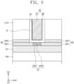
- FIGS. 5 to 9 illustrate cross-sectional views taken along line I-I' of FIG. 1 , showing stages in a method of fabricating a semiconductor device according to some embodiments.
- FIGS. 1 to 4 and 5 to 9 the following will describe in detail a method of fabricating a semiconductor device according to some embodiments.
- the oxide layer 101 and a first electrode layer 102 may be sequentially deposited on the substrate 100.
- the first electrode layer 102 may be patterned until at least a portion of the oxide layer 101 is exposed, such that the first source pattern SP1 and the first drain pattern DP1 may be formed.
- the first source pattern SP1 and the first drain pattern DP1 may be spaced apart from each other in the first direction D1.
- the first electrode layer 102 may be patterned to form the channel layer CH in a space that exposes at least a portion of the oxide layer 101, e.g., the channel layer CH may separate the first source pattern SP1 and the first drain pattern DP1 from each other.
- the formation of the channel layer CH may include forming, e.g., conformally forming, a first channel layer in the space that exposes the portion of the oxide layer 101, on a top surface of the first source pattern SP1, and on a top surface of the first drain pattern DP1, forming a second channel layer on the first channel layer, and partially removing each of the first and second channel layers by performing a planarization process until exposure of the top surface of the first source pattern SP1 and the top surface of the first drain pattern DP1.
- the partial removal of each of the first and second channel layers may form the first and second channel patterns CHP1 and CHP2.
- the channel layer CH may have a top surface substantially coplanar with that of the first source pattern SP1 and that of the first drain pattern DP1.
- the planarization process may include, e.g., a chemical mechanical polishing (CMP) process or an etch-back process.
- a second electrode layer 103 may be formed to cover the channel layer CH, the first source pattern SP1, and the first drain pattern DP1.
- the second electrode layer 103 may be formed of the same material as that of the first source pattern SP1 and the first drain pattern DP1.
- the first interlayer dielectric layer ILD1 may be formed on the second electrode layer 103.
- a gate hole GH may be formed to penetrate the first interlayer dielectric layer ILD1 and the second electrode layer 103, and thus the second source pattern SP2 and the second drain pattern DP2 may be formed.
- the source electrode SE may be formed which includes the first source pattern SP1 and the second source pattern SP2
- the drain electrode DE may be formed which includes the first drain pattern DP1 and the second drain pattern DP2.
- the second source pattern SP2 and the second drain pattern DP2 may be spaced apart from each other in the first direction D1.
- the gate hole GH may expose at least a portion of the top surface of the first source pattern SP1, at least a portion of the top surface of the first drain pattern DP1, and the top surface of the channel layer CH.
- a width in the first direction D1 of the gate hole GH may be greater than a width in the first direction D1 of the channel layer CH.
- the gate dielectric pattern GI may be conformally formed in the gate hole GH.
- the gate electrode GE may be formed to fill a space in the gate hole GH in which the gate dielectric pattern GI is formed to surround the space.
- the formation of the gate electrode GE may include forming the barrier pattern BP that conformally covers the space that is in the gate hole GH and is surrounded by the gate dielectric pattern GI, and forming the conductive pattern CP that fills the space in the gate hole GH in which the barrier pattern BP is formed to surround the space.
- the gate electrode GE may have a top surface substantially coplanar with that of the gate dielectric pattern GI and that of the first interlayer dielectric layer ILD1.
- the second interlayer dielectric layer ILD2 may be formed on the gate electrode GE and the first interlayer dielectric layer ILD1.
- the source contact SC and the drain contact DC may be formed to penetrate the first and second interlayer dielectric layers ILD1 and ILD2.
- the formation of each of the source and drain contacts SC and DC may include conformally forming the barrier pattern BP and forming the conductive pattern CP that surrounds the barrier pattern BP.
- the third interlayer dielectric layer ILD3 may be formed to cover the second interlayer dielectric layer ILD2, the source contact SC, and the drain contact DC.
- Wiring lines ML may be formed in the third interlayer dielectric layer ILD3.
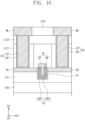
- FIG. 10 illustrates a cross-sectional view taken along line I-I' of FIG. 1 , showing a semiconductor device according to some embodiments.
- FIG. 10 illustrates a cross-sectional view taken along line I-I' of FIG. 1 , showing a semiconductor device according to some embodiments.
- the gate electrode GE may have a T-shaped structure in which at least a portion of the gate electrode GE is buried in the oxide layer 101.
- the portion of the gate electrode GE buried in the oxide layer 101 may be located at, e.g., may extend to, a level lower than that of a bottom surface of the source electrode SE and lower than a bottom surface of the drain electrode DE.
- the portion of the gate electrode GE buried in, e.g., extending into, the oxide layer 101 may overlap in the first direction D1 (or horizontally) with the source electrode SE and the drain electrode DE across the channel layer CH.
- the channel layer CH may include first and second channel patterns CHP1 and CHP2 that conformally cover a bottom surface and opposite sidewalls of the gate electrode GE.
- the gate dielectric pattern GI may be interposed between the channel layer CH and the gate electrode GE.
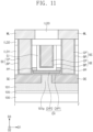
- FIG. 11 illustrates a cross-sectional view taken along line I-I' of FIG. 1 , showing a semiconductor device according to some embodiments.
- FIGS. 1 to 4 For convenience of description, a description of contents substantially the same as that discussed with reference to FIGS. 1 to 4 will be omitted, and a difference thereof will be discussed in detail.
- the oxide layer 101 may include a protrusion 101p that protrudes in the third direction D3.
- the protrusion 101p of the oxide layer 101 may be positioned between the source electrode SE and the drain electrode DE.
- the protrusion 101p of the oxide layer 101 may have a top surface substantially coplanar with that of the source electrode SE and that of the drain electrode DE.
- the source contact SC and the drain contact DC may be provided therebetween with the channel layer CH that covers the protrusion 101p of the oxide layer 101, and covers a portion of the source electrode SE, and a portion of the drain electrode DE.
- Each of sidewalls of the channel layer CH may be in contact with the source contact SC or the drain contact DC.
- the gate electrode GE may be provided on the channel layer CH. At least a portion of the gate electrode GE may overlap in the third direction D3 with at least a portion of the source electrode SE. At least a portion of the gate electrode GE may overlap in the third direction D3 with at least a portion of the drain electrode DE.
- the gate dielectric pattern GI may be interposed between the gate electrode GE and the channel layer CH, and may extend in the third direction D3 along opposite sidewalls of the gate electrode GE.
- Passivation patterns PP may be provided between the source contact SC and the gate electrode GE and between the drain contact DC and the gate electrode GE.
- the passivation patterns PP may extend in the second direction D2 along opposite sidewalls of the gate electrode GE on the channel layer CH.
- the passivation patterns PP may be in direct contact with the top surface of the channel layer CH.
- Each of the passivation patterns PP may overlap in the third direction D3 (or vertically) with the source electrode SE or the drain electrode DE.
- the passivation patterns PP may minimize and/or prevent hydrogen from entering the channel layer CH in a subsequent process (or annealing process).
- the passivation patterns PP may include, e.g., silicon nitride or aluminum oxide.
- FIG. 12 illustrates a cross-sectional view taken along line I-I' of FIG. 1 , showing a semiconductor device according to some embodiments.
- FIGS. 1 to 4 and 11 For convenience of description, a description of contents substantially the same as that discussed with reference to FIGS. 1 to 4 and 11 will be omitted, and a difference thereof will be discussed in detail.
- the first channel pattern CHP1 of the channel layer CH may not be formed on the top surface of the protrusion 101p of the oxide layer 101.
- the first channel pattern CHP1 of the channel layer CH may be selectively provided on the top surface of the source electrode SE and on the top surface of the drain electrode DE.
- At least a portion of the second channel pattern CHP2 of the channel layer CH may be in direct contact with the top surface of the protrusion 101p of the oxide layer 101.
- FIGS. 13 and 14 illustrate cross-sectional views showing a semiconductor device according to some embodiments.
- FIG. 15 illustrates a perspective view showing a semiconductor device according to some embodiments. With reference to FIGS. 13 to 15 , the following will describe implemented examples of a semiconductor device according to some embodiments.
- the semiconductor memory cell may be, e.g., a dynamic random access memory (DRAM) cell.
- the semiconductor memory cell may include the semiconductor devices 10 on the substrate 100, according to embodiments, and may also include a capacitor CAP connected to the semiconductor devices 10.
- the substrate 100 may be provided thereon with the semiconductor devices 10 according to embodiments.
- a pair of neighboring semiconductor devices 10 may share the source electrode SE.
- the source electrode SE may be provided between the pair of neighboring semiconductor devices 10.
- the substrate 100 may be provided thereon with a first dielectric layer 110 that covers the semiconductor devices 10 according to embodiments.
- the first dielectric layer 110 may include at least one of, e.g., silicon oxide, silicon nitride, and silicon oxynitride.
- Bit lines BL may be provided in the first dielectric layer 110. Each of the bit lines BL may be provided on the source electrode SE that is shared by a pair of neighboring semiconductor devices 10.
- the bit lines BL may include at least one of, e.g., doped semiconductor materials, conductive metal nitrides, metallic materials, and metal-semiconductor compounds.
- Landing pads LP may be provided in the first dielectric layer 110. Each of the landing pads LP may be provided on the drain electrode DE of the semiconductor device 10. Each of the landing pads LP may include a conductive material, e.g., metal or doped silicon.
- the capacitor CAP may be provided on the first dielectric layer 110.
- the capacitor CAP may include bottom electrodes BE, a top electrode TE, and a dielectric layer DL interposed between the bottom electrodes BE and the top electrode TE.
- the bottom electrodes BE may be provided on corresponding landing pads LP. Each of the bottom electrodes BE may be electrically connected to the drain electrode DE through one of the landing pads LP.
- the bottom electrodes BE may be linearly arranged along the first direction D1.
- Each of the bottom electrodes BE may have a cylindrical (or cup) shape that has a bottom portion and a sidewall portion that vertically extends from the bottom portion.
- the bottom portion and the sidewall portion of each bottom electrode BE may have substantially the same thickness.
- the bottom electrodes BE may have substantially the same diameter.
- the bottom electrodes BE may include at least one of, e.g., doped semiconductor materials, conductive metal nitrides, metallic materials, and metal-semiconductor compounds.
- the bottom electrodes BE may include a metal nitride layer, e.g., a titanium nitride (TiN) layer, a titanium silicon nitride (TiSiN) layer, a titanium aluminum nitride (TiAlN) layer, a tantalum nitride (TaN) layer, a tantalum silicon nitride (TaSiN) layer, a tantalum aluminum nitride (TaAlN) layer, and a tungsten nitride (WN) layer.
- TiN titanium nitride
- TiSiN titanium silicon nitride
- TiAlN titanium aluminum nitride
- TaN tantalum nitride
- TaSiN tantalum silicon
- the dielectric layer DL may be provided to have a uniform thickness on surfaces of the bottom electrodes BE and on exposed surfaces of the first dielectric layer 110.
- the dielectric layer DL may include a high-k dielectric material, e.g., HfO 2 , ZrO 2 , Al 2 O 3 , La 2 O 3 , Ta 2 O 3 , and TiO 2 .
- the top electrode TE may be provided on the dielectric layer DL.
- the top electrode TE may cover a plurality of bottom electrodes BE across the dielectric layer DL. Portions of the top electrode TE may fill inside spaces of the bottom electrodes BE.
- the top electrode TE may include at least one of, e.g., doped semiconductor materials, conductive metal nitrides, metallic materials, and metal-semiconductor compounds.
- the top electrode TE may have a structure in which a metal nitride and a semiconductor material are sequentially stacked.
- a front-end-of-line (FEOL) process may be performed to form the semiconductor devices 10, the first dielectric layer 110, the landing pads LP, and the capacitor CAP on the substrate 100.
- FEOL front-end-of-line
- Second, third, fourth, and fifth dielectric layers 120, 130, 140, and 150 may be stacked on the capacitor CAP.
- the second dielectric layer 120 may be provided therein with at least one contact CT that penetrates the second dielectric layer 120 and electrically connects to the top electrode TE.
- the third, fourth, and fifth dielectric layers 130, 140, and 150 may be provided therein with wiring lines IL, vias VI, and the semiconductor devices 10 according to embodiments.
- the semiconductor device 10 may be provided in one of the second, third, fourth, and fifth dielectric layers 120, 130, 140, and 150, and may be electrically connected to one of the wiring lines IL.
- the vias VI may vertically connect the wiring lines IL to each other.
- the wiring lines IL of the semiconductor memory cell may be electrically connected through a contact CT to the capacitor CAP.
- a back-end-of-line (BEOL) process may be performed to form the wiring lines IL, the semiconductor devices 10, and the vias VI provided in the second, third, fourth, and fifth dielectric layers 120, 130, 140, and 150.
- BEOL back-end-of-line
- the image sensor chip may include a first sub-chip SCH1, a second sub-chip SCH2, and an insert layer 300.
- the first sub-chip SCH1 may include the first substrate 100, a circuit layer LL on the first substrate 100, and the first, second, third, fourth, and fifth dielectric layers 110, 120, 130, 140, and 150 on the first substrate 100.
- the circuit layer LL may include the semiconductor devices 10 according to embodiments.
- the semiconductor devices 10 may be spaced apart from each other and two-dimensionally arranged on the first substrate 100.
- the semiconductor devices 10 may be logic transistors that process signals transmitted from the second sub-chip SCH2.
- the first, second, third, fourth, and fifth dielectric layers 110, 120, 130, 140, and 150 may be sequentially provided on the circuit layer LL.
- Lower wiring lines EP may be provided in the first dielectric layer 110.
- One of the lower wiring lines EP may be commonly provided on a source electrode and a drain electrode of neighboring semiconductor devices 10.
- a drain electrode and a source electrode of a pair of neighboring semiconductor devices 10 may be electrically connected to each other through one of the lower wiring lines EP.
- a drain electrode DE that is not connected to the lower wiring lines EP may penetrate the first dielectric layer 110.
- the lower wiring line EP may include a conductive material, e.g., doped silicon or metal.
- At least one contact CT may be provided to penetrate the second dielectric layer 120 and to electrically connect to the drain electrode DE that is not connected to the lower wiring lines EP.
- Wiring lines IL and vias VI may be provided in the third, fourth, and fifth dielectric layers 130, 140, and 150.
- the vias VI may vertically connect the wiring lines IL to each other.
- the wiring lines IL of the first sub-chip SCH1 may be electrically connected through the contact CT to the semiconductor device 10 in the circuit layer LL.
- the second sub-chip SCH2 may include photoelectric conversion elements PCD, floating diffusion regions FDA, and readout circuit elements RCX, all of which components are formed on a second substrate 200.
- the second substrate 200 may be a semiconductor substrate doped with impurities to have a second conductivity type (e.g., p-type).
- the readout circuit elements RCX may be provided on a first surface 200a of the second substrate 200.
- the readout circuit elements RCX may include a plurality of transistors each of which transfer and amplify an electrical signal (e.g., photo-charge) that corresponds to incident light.
- the second surface 200b of the second substrate 200 may be provided thereon with color filters CF and microlenses L.
- the color filters CF and microlenses L provide the photoelectric conversion element PCD with incident light.
- the second surface 200b may be opposite to the first surface 200a.
- Each of the photoelectric conversion elements PCD may include a photodiode.
- the photoelectric conversion elements PCD may be provided in the second substrate 200.
- the photoelectric conversion elements PCD may generate photo-charges corresponding to incident light.
- each of the photoelectric conversion elements PCD may generate an electron-hole pair corresponding to incident light.
- the photoelectric conversion elements PCD may be doped with impurities to have a second conductivity type (e.g., n-type) different from that of the second substrate 200.
- the color filters CF may be provided on corresponding photoelectric conversion elements PCD.
- the color filters CF may be arranged in a matrix shape to constitute a color filter array.
- the color filter array may include a Bayer pattern consisting of a red filter, a green filter, and a blue filter.
- Each of the color filters CF may be one of the red, green, and blue filters.
- the color filter array may include a Bayer pattern consisting of a yellow filter, a magenta filter, and a cyan filter.
- Each of the color filters CF may be one of the yellow, magenta, and cyan filters.
- the microlenses L may be provided on corresponding color filters CF.
- the microlens L may control a path of light incident thereon in such a way that the incident light is directed to the photoelectric conversion element PCD that underlies the microlens L.
- the microlenses L may be arranged in a matrix shape to constitute a microlens array.
- An antireflective layer 205 may be provided between the color filters CF and the second surface 200b of the second substrate 200.
- the antireflective layer 205 may minimize and/or prevent incident light from being reflected on the second surface 200b of the second substrate 200.
- the antireflective layer 205 may have a multi-layered structure where materials having different refractive indices are alternately stacked. The antireflective layer 205 may improve its transmittance with increasing the number of stacked materials having different refractive indices.
- First, second, third, and fourth upper dielectric layers 210, 220, 230, and 240 may be stacked on the first surface 200a of the second substrate 200.
- Wiring lines II, and vias VI may be provided in the first, second, third, and fourth upper dielectric layers 210, 220, 230, and 240.
- the vias VI may vertically connect the wiring lines II, to each other.
- the wiring lines II, of the second sub-chip SCH2 may be electrically connected to the readout circuit elements RCX.
- the photoelectric conversion elements PCD of the second sub-chip SCH2 may generate photo-charges in response to light incident on the second surface 200b of the second substrate 200.
- the image sensor chip according to the present embodiment may be a backside illuminated image sensor (BIS).
- An interconnector 310 may be included in the insert layer 300 between the first and second sub-chips SCH1 and SCH2.
- the interconnector 310 may electrically connect the wiring lines IL of the first sub-chip SCH1 to the wiring lines IL of the second sub-chip SCH2.
- the interconnector 310 may include metal, e.g., copper and/or tungsten.
- the interconnector 310 may include a first conductive pattern 310a electrically connected to at least one wiring line IL of the first sub-chip SCH1 and a second conductive pattern 310b electrically connected to at least one wiring line IL of the second sub-chip SCH2.
- the first and second conductive patterns 310a and 310b may be in contact with each other and thereby electrically connected to each other.
- the insert layer 300 may further include a first dielectric layer 350a and a second dielectric layer 350b.
- the first and second conductive patterns 310a and 310b may be provided respectively in the first and second dielectric layers 350a and 350b.
- the first and second dielectric layers 350a and 350b may include, e.g., silicon oxide.
- the insert layer 300 may further include a first metal diffusion break layer 360a, a second metal diffusion break layer 360b, and a third metal diffusion break layer 360c.
- the first metal diffusion break layer 360a may be interposed between the first sub-chip SCH1 and the first dielectric layer 350a
- the second metal diffusion break layer 360b may be interposed between the first dielectric layer 350a and the second dielectric layer 350b
- the third metal diffusion break layer 360c may be interposed between the second dielectric layer 350b and the second sub-chip SCH2.
- the first, second, and third metal diffusion break layers 360a, 360b, and 360c may include, e.g., SiN, SiCN, SiOCN, SiON, or SiC.
- the first, second, and third metal diffusion break layers 360a, 360b, and 360c may minimize and/or prevent metal constituents from being diffused from the interconnector 310.
- the semiconductor apparatus may include a cell array structure CS and a peripheral circuit structure PS.
- the peripheral circuit structure PS may be stacked on the cell array structure CS.
- the peripheral circuit structure PS and the cell array structure CS may, e.g., vertically, overlap each other.
- the peripheral circuit structure PS of the semiconductor apparatus may be provided below the cell array structure CS of the semiconductor apparatus.
- the cell array structure CS may include a plurality of memory cells.
- the plurality of memory cells may include one or more semiconductor memory cells, or DRAM cells, discussed with reference to FIG. 13 .
- the memory cells may include a NAND cell or a static random access memory (SRAM) cell.
- the peripheral circuit structure PS may include, e.g., a row decoder, a column decoder, a page buffer, and a control circuit that control a cell array. Circuits included in the peripheral circuit structure PS may be formed of the semiconductor devices 10 according to embodiments.
- embodiments provide a semiconductor device with improved electrical properties and increased reliability, a method of fabricating the same, and a semiconductor memory cell including the same. That is, according to embodiments, a lower contact resistance and a high mobility may be obtained through a channel layer that includes channel patterns including, e.g., consisting of, different oxide semiconductor materials from each other. In addition, according to embodiments, a portion of a source electrode and a portion of a drain electrode may overlap a portion of a gate electrode, and thus resistance between a source/drain and a channel may be reduced to complement a low mobility of an oxide semiconductor material. Accordingly, it may be possible to improve reliability and electrical properties of a semiconductor device and a semiconductor memory cell including the same according to embodiments.
Landscapes
- Thin Film Transistor (AREA)
- Electrodes Of Semiconductors (AREA)
- Non-Volatile Memory (AREA)
- Semiconductor Memories (AREA)
Description
- Example embodiments of the present disclosure relate to a semiconductor device and a semiconductor memory cell including the same, and more particularly, to a semiconductor device including an oxide semiconductor transistor structure, a method of fabricating the same, and a semiconductor memory cell including the same.
- A transistor may be used as a switching device or a driving device in the electronic device field. In particular, because a thin film transistor can be manufactured even on a glass substrate or a plastic substrate, the thin film transistor is valuably utilized in the field of displays, e.g., in an organic light emitting display or a liquid crystal display.
- The performance of a thin film transistor mainly depends on physical properties of a channel layer (e.g., a semiconductor layer). Therefore, a thin film transistor having excellent performance is required to achieve semiconductor circuits of next-generation high performance and integration, and in connection with this, research is being conducted on an oxide thin film transistor in which an oxide semiconductor with high carrier mobility is used as a material for the channel layer.
-
US20120187395A1 describes a semiconductor element having high mobility, which includes an oxide semiconductor layer having crystallinity. The oxide semiconductor layer includes a stacked-layer structure of a first oxide semiconductor film and a second oxide semiconductor film having a wider band gap than the first oxide semiconductor film, which is in contact with the first oxide semiconductor film. Thus, a channel region is formed in part of the first oxide semiconductor film (that is, in an oxide semiconductor film having a smaller band gap) which is in the vicinity of an interface with the second oxide semiconductor film. Further, dangling bonds in the first oxide semiconductor film and the second oxide semiconductor film are bonded to each other at the interface therebetween. -
US20080191204A1 describes a transistor which may include: a gate insulting layer; a gate electrode formed on the gate insulating layer; a channel layer formed on the gate insulating layer; and source and drain electrodes that contact the channel layer. The channel layer may have a double-layer structure, including upper and lower layers. The upper layer may have a carrier concentration lower than the lower layer. A method of manufacturing a transistor may include: forming a channel layer on a substrate; forming source and drain electrodes on the substrate; forming a gate insulating layer on the substrate; and forming a gate electrode on the gate insulating layer above the channel layer. A method of manufacturing a transistor may include: forming a gate electrode on a substrate; forming a gate insulating layer on the substrate; forming a channel layer on the gate insulating layer; and forming source and drain electrodes on the gate insulating layer. - According to some embodiments, a semiconductor device is as defined in claim 1.
- According to some example embodiments of the present disclosure, a semiconductor device may include a substrate; a gate electrode on the substrate; a channel layer between the substrate and the gate electrode; a source electrode in contact with a first sidewall of the channel layer; and a drain electrode in contact with a second sidewall of the channel layer. The second sidewall may be opposite to the first sidewall. The source electrode and the drain electrode may be spaced apart from each other in a first direction parallel to a top surface of the substrate. The gate electrode may extend in a second direction that intersects the first direction and is parallel to the top surface of the substrate. The channel layer may include a first channel pattern in contact with one of the source electrode and the drain electrode; and a second channel pattern between the first channel pattern and the gate electrode. The first channel pattern and the second channel pattern may include oxide semiconductor materials different from each other. A portion of the source electrode and a portion of the drain electrode may overlap in a third direction with a portion of the gate electrode. The third direction may be perpendicular to the top surface of the substrate.
- According to some example embodiments of the present disclosure, a semiconductor memory cell may include a substrate; a semiconductor device on the substrate; a landing pad on the semiconductor device; and a capacitor that includes a plurality of bottom electrodes, a top electrode, and a dielectric layer between the bottom electrodes and the top electrode. The capacitor may be connected through the landing pad to the semiconductor device. The semiconductor device may include a gate electrode on the substrate; a channel layer between the substrate and the gate electrode; a source electrode in contact with a first sidewall of the channel layer; and a drain electrode in contact with a second sidewall of the channel layer. The second sidewall may be opposite to the first sidewall. The channel layer of the semiconductor device may include a first channel pattern in contact with one of the source electrode and the drain electrode, the first channel pattern including a crystalline oxide semiconductor material; and a second channel pattern between the first channel pattern and the gate electrode, the second channel pattern including an amorphous oxide semiconductor material. A portion of the source electrode and a portion of the drain electrode may overlap a portion of the gate electrode.
- At least some of the above and other features of the invention are set out in the claims.
- Features will become apparent to those of skill in the art by describing in detail example embodiments with reference to the attached drawings, in which:
-
FIG. 1 illustrates a plan view showing a semiconductor device according to some embodiments. -
FIGS. 2 and3 illustrate cross-sectional views respectively taken along lines I-I' and II-II' ofFIG. 1 . -
FIG. 4 illustrates an enlarged view of section A inFIG. 2 , partially showing a semiconductor device according to some embodiments. -
FIGS. 5 to 9 illustrate cross-sectional views of stages in a method of fabricating a semiconductor device according to some embodiments. -
FIGS. 10 to 12 illustrate cross-sectional views along line I-I' ofFIG. 1 , showing a semiconductor device according to some embodiments. -
FIGS. 13 and14 illustrate cross-sectional views showing a semiconductor device according to some embodiments. -
FIG. 15 illustrates a perspective view showing a semiconductor device according to some embodiments. - With reference to the accompanying drawings, the following will describe in detail a semiconductor device, a method of fabricating the same, and a semiconductor memory cell including the same according to some embodiments.
-
FIG. 1 illustrates a plan view showing a semiconductor device according to some embodiments.FIGS. 2 and3 illustrate cross-sectional views along lines I-I' and II-II' ofFIG. 1 , respectively. - Referring to
FIGS. 1 ,2 , and3 , asemiconductor device 10 according to embodiments may include a channel layer CH, a gate electrode GE, a source electrode SE, and a drain electrode DE that are provided on asubstrate 100. Thesemiconductor device 10 according to embodiments may have an oxide semiconductor transistor structure. - The
substrate 100 may be, e.g., a semiconductor substrate, a glass substrate, or a plastic substrate. The semiconductor substrate may include, e.g., one or more of silicon, germanium, and silicon-germanium. According to some embodiments, thesubstrate 100 may be a silicon wafer. Thesubstrate 100 may have a top surface that is parallel to a first direction D1 and a second direction D2 that intersects the first direction D1, and is perpendicular to a third direction D3. The first, second, and third directions D1, D2, and D3 may be, e.g., orthogonal directions to each other. - The
semiconductor device 10 according to embodiments may be formed in a front-end-of-line (FEOL) layer, in a back-end-of-line (BEOL) layer, or in a peripheral circuit structure on thesubstrate 100. - An
oxide layer 101 may be provided on thesubstrate 100. Theoxide layer 101 may include, e.g., silicon oxide. According to some embodiments, theoxide layer 101 may be provided in thesubstrate 100. - A channel layer CH may be provided on the
substrate 100. The channel layer CH may include an oxide semiconductor material. The channel layer CH may include, e.g., a compound of oxygen (O) and at least two metals selected from zinc (Zn), indium (In), gallium (Ga), and tin (Sn). - The channel layer CH may include a first channel pattern CHP1 and a second channel pattern CHP2. The second channel pattern CHP2 may be provided on the first channel pattern CHP1. The first channel pattern CHP1 may cover a bottom surface and opposite sidewalls of the second channel pattern CHP2, e.g., the first channel pattern CHP1 may extend continuously along the entire bottom surface and opposite sidewalls of the second channel pattern CHP2. For example, as illustrated in
FIGS. 2 and3 , the first channel pattern CHP1 may be conformal along the bottom surface and opposite sidewalls of the second channel pattern CHP2, and a thickness of the second channel pattern CHP2 along the third direction D3 may be larger than a thickness of a horizontal portion of first channel pattern CHP1 (i.e., a part of first channel pattern CHP1 directly under the second channel pattern CHP2) along the third direction D3. For example, as illustrated inFIGS. 2 and3 , uppermost surfaces of the first and second channel patterns CHP1 and CHP2 may be coplanar. - The first and second channel patterns CHP1 and CHP2 may include oxide semiconductor materials that are different from each other. For example, the first channel pattern CHP1 may include a crystalline oxide semiconductor material, and the second channel pattern CHP2 may include an amorphous oxide semiconductor material. The first channel pattern CHP1 may have a contact resistance less than that of the second channel pattern CHP2. The second channel pattern CHP2 may have a carrier mobility, e.g., a measure of how quickly a charge carrier can move through a material, greater than that of the first channel pattern CHP1.
- For example, the first channel pattern CHP1 may include c-axis aligned crystal indium-gallium-zinc oxide (CAAC-IGZO) or indium-tin oxide (ITO), and the second channel pattern CHP2 may include indium-gallium-zinc oxide (IGZO), In2O3, or indium-tungsten oxide (IWO). According to some embodiments, the second channel pattern CHP2 may include an oxide semiconductor material whose constitution ratio of indium(In) is equal to or greater than about 33.3%.
- The source electrode SE and the drain electrode DE may be provided on opposite sides of the channel layer CH. The source electrode SE and the drain electrode DE may be in direct contact with a sidewall of the channel layer CH.
- The source electrode SE may include a first source pattern SP1 on the
substrate 100 and a second source pattern SP2 on the first source pattern SP1. The source electrode SE may have a step difference at an interface between the first source pattern SP1 and the second source pattern SP2. For example, at least a portion of the first source pattern SP1 may be exposed without being covered with the second source pattern SP2. For example, a length in the first direction D1 of the first source pattern SP1 may be greater than a length in the first direction D1 of the second source pattern SP2. The first source pattern SP1 may be in contact with the channel layer CH. A bottom surface of the first source pattern SP1 may be substantially coplanar with that of the channel layer CH. A top surface of the first source pattern SP1 (or, a bottom surface of the second source pattern SP2) may be substantially coplanar with that of the channel layer CH. A portion of the first source pattern SP1 may overlap in the third direction (or vertically) with a portion of the gate electrode GE. - The drain electrode DE may include a first drain pattern DP1 on the
substrate 100 and a second drain pattern DP2 on the first drain pattern DP1. The drain electrode DE may have a step difference at an interface between the first drain pattern DP1 and the second drain pattern DP2. For example, at a portion of the first drain pattern DP1 may be exposed without being covered with the second drain pattern DP2. For example, a length in the first direction D1 of the first drain pattern DP1 may be greater than a length in the first direction D1 of the second drain pattern DP2. The first drain pattern DP1 may be in contact with the channel layer CH. A bottom surface of the first drain pattern DP1 may be substantially coplanar with that of the channel layer CH. A top surface of the first drain pattern DP1 (or, a bottom surface of the second drain pattern DP2) may be substantially coplanar with that of the channel layer CH. A portion of the first drain pattern DP1 may overlap in the third direction D3 (or vertically) with a portion of the gate electrode GE. - The first drain pattern DP1 may be spaced apart in the first direction D1 from the first source pattern SP1 of the source electrode SE across the channel layer CH. The second drain pattern DP2 may be spaced apart in the first direction D1 from the second source pattern SP2 of the source electrode SE across the gate electrode GE and a gate dielectric pattern GI which will be discussed below. For example, as illustrated in
FIGS. 2 and4 , the first channel pattern CHP1 may separate the second channel pattern CHP2 from each of the first source pattern SP1 and the first drain pattern DP1. - The source electrode SE and the drain electrode DE may include a conductive material. For example, the source electrode SE and the drain electrode DE may include at least one of doped semiconductor materials (e.g., doped silicon, doped germanium, etc.), conductive metal nitrides (e.g., titanium nitride, tantalum nitride, tungsten nitride, etc.), and metallic materials (e.g., titanium, tantalum, tungsten, copper, aluminum, ruthenium, molybdenum, etc.).
- A first interlayer dielectric layer ILD1 may be provided to cover the source electrode SE and the drain electrode DE. The first interlayer dielectric layer ILD1 may include at least one of, e.g., silicon oxide, silicon nitride, and silicon oxynitride.
- The gate electrode GE may be provided to penetrate the first interlayer dielectric layer ILD1 and to extend, e.g., lengthwise, in the second direction D2. The gate electrode GE may be positioned between the source electrode SE and the drain electrode DE. At least a portion of the gate electrode GE may overlap in the third direction D3 with the first source pattern SP1 of the source electrode SE and with the first drain pattern DP1 of the drain electrode DE. In addition, at least a portion of the gate electrode GE may overlap in the first direction D1 with the second source pattern SP2 of the source electrode SE and with the second drain pattern DP2 of the drain electrode DE. The gate electrode GE may cover the channel layer CH, e.g., completely cover the top surface of the channel layer CH. A width in the first direction D1 of the gate electrode GE may be greater than a width in the first direction D1 of the channel layer CH. A length in the second direction D2 of the gate electrode GE may be greater than a length in the second direction D2 of the channel layer CH. At least a portion, e.g., an edge, of the gate electrode GE may protrude toward the
substrate 100, e.g., in the third direction D3, and may overlap in the second direction D2 with the channel layer CH. - The gate electrode GE may include a barrier pattern BP and a conductive pattern CP. The barrier pattern BP may cover sidewalls and a bottom surface of the conductive pattern CP. The barrier pattern BP may include a metal layer and a metal nitride layer. The metal layer may include, e.g., at least one of titanium, tantalum, tungsten, nickel, cobalt, and platinum. The metal nitride layer may include, e.g., at least one of titanium nitride (TiN), tantalum nitride (TaN), tungsten nitride (WN), nickel nitride (NiN), cobalt nitride (CoN), and platinum nitride (PtN). The conductive pattern CP may include, e.g., at least one metal of aluminum, copper, tungsten, molybdenum, and cobalt. According to some embodiments, the barrier pattern BP of the gate electrode GE may include the same material as that of the source electrode SE and the drain electrode DE.
- A gate dielectric pattern GI may be provided to cover a bottom surface and opposite sidewalls of the gate electrode GE. The gate dielectric pattern GI may be interposed between the gate electrode GE and the first interlayer dielectric layer ILD1 and between the gate electrode GE and the channel layer CH. A bottom surface of the gate dielectric pattern GI may be in direct contact with the top surface of the channel layer CH. A top surface of the gate dielectric pattern GI may be substantially coplanar with that of the gate electrode GE and that of the first interlayer dielectric layer ILD1. The gate dielectric pattern GI may include a material having good interfacial characteristics with an oxide semiconductor material of the channel layer CH, and may minimize and/or prevent hydrogen from entering the channel layer CH in a subsequent process (e.g., annealing process). The gate dielectric pattern GI may include, e.g., at least one of silicon oxide, silicon nitride, silicon oxynitride, and high-k dielectric. The high-k dielectric may be a material with a dielectric constant that is greater than that of silicon oxide or silicon nitride, e.g., hafnium oxide, aluminum oxide, or tantalum oxide.
- The first interlayer dielectric layer ILD1 may be provided thereon with a second interlayer dielectric layer ILD2 that covers the top surface of the gate electrode GE. The second interlayer dielectric layer ILD2 may include, e.g., at least one of silicon oxide, silicon nitride, and silicon oxynitride.
- The source electrode SE may be provided thereon with a source contact SC that penetrates the first and second interlayer dielectric layers ILD1 and ILD2 and contacts the source electrode SE. The drain electrode DE may be provided thereon with a drain contact DC that penetrates the first and second interlayer dielectric layers ILD1 and ILD2 and contacts the drain electrode DE. The source contact SC and the drain contact DC may have their top surfaces substantially coplanar with that of the second interlayer dielectric layer ILD2. Similar to the gate electrode GE, each of the source contact SC and the drain contact DC may include a barrier pattern BP and a conductive pattern CP. According to some embodiments, the barrier pattern BP of each of the source contact SC and the drain contact DC may include the same material as that of the source electrode SE and the drain electrode DE.
- The second interlayer dielectric layer ILD2 may be provided thereon with a third interlayer dielectric layer ILD3 that covers the top surface of the source contact SC and the top surface of the drain contact DC. The third interlayer dielectric layer ILD3 may include, e.g., at least one of silicon oxide, silicon nitride, and silicon oxynitride. The third interlayer dielectric layer ILD3 may be provided therein with wiring lines ML connected to the source contact SC and the drain contact DC. Each of the wiring lines ML may be electrically connected either through the source contact SC to the source electrode SE or through the drain contact DC to the drain electrode DE. The wiring lines ML may include a conductive material. According to some embodiments, the third interlayer dielectric layers ILD3 may further be provided therein with additional wiring lines connected to the wiring lines ML and with vias that connect the additional wiring lines to each other.
-
FIG. 4 illustrates an enlarged view of section A depicted inFIG. 2 , partially showing a semiconductor device according to some embodiments. - Referring to
FIG. 4 , the conductive pattern CP of the gate electrode GE may include a first portion P1, a second portion P2, and a third portion P3. For example, as illustrated inFIG. 4 , the first through third portions P1 through P3 may be arranged sequentially in the stated order along the first direction D1, and may be integral with each other, i.e., constituting a single, uniform, and seamless (e.g., without a visible interface) element. - In detail, the first portion P1 of the conductive pattern CP may overlap in the third direction D3 with the first source pattern SP1 of the source electrode SE. The first portion P1 of the conductive pattern CP may have one sidewall in, e.g., direct, contact with the barrier pattern BP. The one sidewall of the first portion P1 may be above the first source pattern SP1 of the source electrode SE, and may be horizontally spaced apart along the first direction D1 from an extension of a first sidewall CHs1 of the channel layer CH. The second portion P2 of the conductive pattern CP may overlap in the third direction D3 with the channel layer CH. The second portion P2 of the conductive pattern CP may be positioned between the first portion P1 and the third portion P3 of the conductive pattern CP. The third portion P3 of the conductive pattern CP may overlap in the third direction D3 with the first drain pattern DP1 of the drain electrode DE. The third portion P3 of the conductive pattern CP may have one sidewall in, e.g., direct, contact with the barrier pattern BP that is spaced apart in the first direction D1 from a second sidewall CHs2 of the channel layer CH.
-
FIGS. 5 to 9 illustrate cross-sectional views taken along line I-I' ofFIG. 1 , showing stages in a method of fabricating a semiconductor device according to some embodiments. With reference toFIGS. 1 to 4 and5 to 9 , the following will describe in detail a method of fabricating a semiconductor device according to some embodiments. - Referring to
FIGS. 5 and 6 , theoxide layer 101 and afirst electrode layer 102 may be sequentially deposited on thesubstrate 100. Thefirst electrode layer 102 may be patterned until at least a portion of theoxide layer 101 is exposed, such that the first source pattern SP1 and the first drain pattern DP1 may be formed. The first source pattern SP1 and the first drain pattern DP1 may be spaced apart from each other in the first direction D1. Thefirst electrode layer 102 may be patterned to form the channel layer CH in a space that exposes at least a portion of theoxide layer 101, e.g., the channel layer CH may separate the first source pattern SP1 and the first drain pattern DP1 from each other. - The formation of the channel layer CH may include forming, e.g., conformally forming, a first channel layer in the space that exposes the portion of the
oxide layer 101, on a top surface of the first source pattern SP1, and on a top surface of the first drain pattern DP1, forming a second channel layer on the first channel layer, and partially removing each of the first and second channel layers by performing a planarization process until exposure of the top surface of the first source pattern SP1 and the top surface of the first drain pattern DP1. The partial removal of each of the first and second channel layers may form the first and second channel patterns CHP1 and CHP2. The channel layer CH may have a top surface substantially coplanar with that of the first source pattern SP1 and that of the first drain pattern DP1. Hereinafter, the phrase "substantially coplanar" means that a planarization process has been performed. The planarization process may include, e.g., a chemical mechanical polishing (CMP) process or an etch-back process. - Referring to
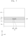
FIG. 7 , asecond electrode layer 103 may be formed to cover the channel layer CH, the first source pattern SP1, and the first drain pattern DP1. Thesecond electrode layer 103 may be formed of the same material as that of the first source pattern SP1 and the first drain pattern DP1. The first interlayer dielectric layer ILD1 may be formed on thesecond electrode layer 103. - Referring to
FIG. 8 , a gate hole GH may be formed to penetrate the first interlayer dielectric layer ILD1 and thesecond electrode layer 103, and thus the second source pattern SP2 and the second drain pattern DP2 may be formed. As a result, the source electrode SE may be formed which includes the first source pattern SP1 and the second source pattern SP2, and the drain electrode DE may be formed which includes the first drain pattern DP1 and the second drain pattern DP2. The second source pattern SP2 and the second drain pattern DP2 may be spaced apart from each other in the first direction D1. The gate hole GH may expose at least a portion of the top surface of the first source pattern SP1, at least a portion of the top surface of the first drain pattern DP1, and the top surface of the channel layer CH. A width in the first direction D1 of the gate hole GH may be greater than a width in the first direction D1 of the channel layer CH. - Referring to
FIG. 9 , the gate dielectric pattern GI may be conformally formed in the gate hole GH. The gate electrode GE may be formed to fill a space in the gate hole GH in which the gate dielectric pattern GI is formed to surround the space. The formation of the gate electrode GE may include forming the barrier pattern BP that conformally covers the space that is in the gate hole GH and is surrounded by the gate dielectric pattern GI, and forming the conductive pattern CP that fills the space in the gate hole GH in which the barrier pattern BP is formed to surround the space. The gate electrode GE may have a top surface substantially coplanar with that of the gate dielectric pattern GI and that of the first interlayer dielectric layer ILD1. - Referring back to
FIGS. 1 to 3 , the second interlayer dielectric layer ILD2 may be formed on the gate electrode GE and the first interlayer dielectric layer ILD1. The source contact SC and the drain contact DC may be formed to penetrate the first and second interlayer dielectric layers ILD1 and ILD2. Similar to the formation of the gate electrode GE, the formation of each of the source and drain contacts SC and DC may include conformally forming the barrier pattern BP and forming the conductive pattern CP that surrounds the barrier pattern BP. Afterward, the third interlayer dielectric layer ILD3 may be formed to cover the second interlayer dielectric layer ILD2, the source contact SC, and the drain contact DC. Wiring lines ML may be formed in the third interlayer dielectric layer ILD3. -
FIG. 10 illustrates a cross-sectional view taken along line I-I' ofFIG. 1 , showing a semiconductor device according to some embodiments. For convenience of description, a description of contents substantially the same as that discussed with reference toFIGS. 1 to 4 will be omitted, and a difference thereof will be discussed in detail. - Referring to
FIG. 10 , the gate electrode GE may have a T-shaped structure in which at least a portion of the gate electrode GE is buried in theoxide layer 101. The portion of the gate electrode GE buried in theoxide layer 101 may be located at, e.g., may extend to, a level lower than that of a bottom surface of the source electrode SE and lower than a bottom surface of the drain electrode DE. The portion of the gate electrode GE buried in, e.g., extending into, theoxide layer 101 may overlap in the first direction D1 (or horizontally) with the source electrode SE and the drain electrode DE across the channel layer CH. The channel layer CH may include first and second channel patterns CHP1 and CHP2 that conformally cover a bottom surface and opposite sidewalls of the gate electrode GE. The gate dielectric pattern GI may be interposed between the channel layer CH and the gate electrode GE. -
FIG. 11 illustrates a cross-sectional view taken along line I-I' ofFIG. 1 , showing a semiconductor device according to some embodiments. For convenience of description, a description of contents substantially the same as that discussed with reference toFIGS. 1 to 4 will be omitted, and a difference thereof will be discussed in detail. - Referring to
FIG. 11 , theoxide layer 101 may include aprotrusion 101p that protrudes in the third direction D3. Theprotrusion 101p of theoxide layer 101 may be positioned between the source electrode SE and the drain electrode DE. Theprotrusion 101p of theoxide layer 101 may have a top surface substantially coplanar with that of the source electrode SE and that of the drain electrode DE. - The source contact SC and the drain contact DC may be provided therebetween with the channel layer CH that covers the
protrusion 101p of theoxide layer 101, and covers a portion of the source electrode SE, and a portion of the drain electrode DE. Each of sidewalls of the channel layer CH may be in contact with the source contact SC or the drain contact DC. The gate electrode GE may be provided on the channel layer CH. At least a portion of the gate electrode GE may overlap in the third direction D3 with at least a portion of the source electrode SE. At least a portion of the gate electrode GE may overlap in the third direction D3 with at least a portion of the drain electrode DE. The gate dielectric pattern GI may be interposed between the gate electrode GE and the channel layer CH, and may extend in the third direction D3 along opposite sidewalls of the gate electrode GE. - Passivation patterns PP may be provided between the source contact SC and the gate electrode GE and between the drain contact DC and the gate electrode GE. The passivation patterns PP may extend in the second direction D2 along opposite sidewalls of the gate electrode GE on the channel layer CH. The passivation patterns PP may be in direct contact with the top surface of the channel layer CH. Each of the passivation patterns PP may overlap in the third direction D3 (or vertically) with the source electrode SE or the drain electrode DE. The passivation patterns PP may minimize and/or prevent hydrogen from entering the channel layer CH in a subsequent process (or annealing process). The passivation patterns PP may include, e.g., silicon nitride or aluminum oxide.
-
FIG. 12 illustrates a cross-sectional view taken along line I-I' ofFIG. 1 , showing a semiconductor device according to some embodiments. For convenience of description, a description of contents substantially the same as that discussed with reference toFIGS. 1 to 4 and11 will be omitted, and a difference thereof will be discussed in detail. - Referring to
FIG. 12 , the first channel pattern CHP1 of the channel layer CH may not be formed on the top surface of theprotrusion 101p of theoxide layer 101. For example, the first channel pattern CHP1 of the channel layer CH may be selectively provided on the top surface of the source electrode SE and on the top surface of the drain electrode DE. At least a portion of the second channel pattern CHP2 of the channel layer CH may be in direct contact with the top surface of theprotrusion 101p of theoxide layer 101. -
FIGS. 13 and14 illustrate cross-sectional views showing a semiconductor device according to some embodiments.FIG. 15 illustrates a perspective view showing a semiconductor device according to some embodiments. With reference toFIGS. 13 to 15 , the following will describe implemented examples of a semiconductor device according to some embodiments. - Referring to
FIG. 13 a semiconductor memory cell includingsemiconductor devices 10 according to embodiments may be illustrated. The semiconductor memory cell may be, e.g., a dynamic random access memory (DRAM) cell. The semiconductor memory cell may include thesemiconductor devices 10 on thesubstrate 100, according to embodiments, and may also include a capacitor CAP connected to thesemiconductor devices 10. - The
substrate 100 may be provided thereon with thesemiconductor devices 10 according to embodiments. A pair of neighboringsemiconductor devices 10 may share the source electrode SE. For example, the source electrode SE may be provided between the pair of neighboringsemiconductor devices 10. - The
substrate 100 may be provided thereon with a firstdielectric layer 110 that covers thesemiconductor devices 10 according to embodiments. Thefirst dielectric layer 110 may include at least one of, e.g., silicon oxide, silicon nitride, and silicon oxynitride. - Bit lines BL may be provided in the
first dielectric layer 110. Each of the bit lines BL may be provided on the source electrode SE that is shared by a pair of neighboringsemiconductor devices 10. The bit lines BL may include at least one of, e.g., doped semiconductor materials, conductive metal nitrides, metallic materials, and metal-semiconductor compounds. - Landing pads LP may be provided in the
first dielectric layer 110. Each of the landing pads LP may be provided on the drain electrode DE of thesemiconductor device 10. Each of the landing pads LP may include a conductive material, e.g., metal or doped silicon. - The capacitor CAP may be provided on the
first dielectric layer 110. The capacitor CAP may include bottom electrodes BE, a top electrode TE, and a dielectric layer DL interposed between the bottom electrodes BE and the top electrode TE. The bottom electrodes BE may be provided on corresponding landing pads LP. Each of the bottom electrodes BE may be electrically connected to the drain electrode DE through one of the landing pads LP. The bottom electrodes BE may be linearly arranged along the first direction D1. - Each of the bottom electrodes BE may have a cylindrical (or cup) shape that has a bottom portion and a sidewall portion that vertically extends from the bottom portion. The bottom portion and the sidewall portion of each bottom electrode BE may have substantially the same thickness. When viewed in a plan view, the bottom electrodes BE may have substantially the same diameter.
- The bottom electrodes BE may include at least one of, e.g., doped semiconductor materials, conductive metal nitrides, metallic materials, and metal-semiconductor compounds. For example, the bottom electrodes BE may include a metal nitride layer, e.g., a titanium nitride (TiN) layer, a titanium silicon nitride (TiSiN) layer, a titanium aluminum nitride (TiAlN) layer, a tantalum nitride (TaN) layer, a tantalum silicon nitride (TaSiN) layer, a tantalum aluminum nitride (TaAlN) layer, and a tungsten nitride (WN) layer.
- The dielectric layer DL may be provided to have a uniform thickness on surfaces of the bottom electrodes BE and on exposed surfaces of the
first dielectric layer 110. The dielectric layer DL may include a high-k dielectric material, e.g., HfO2, ZrO2, Al2O3, La2O3, Ta2O3, and TiO2. - The top electrode TE may be provided on the dielectric layer DL. The top electrode TE may cover a plurality of bottom electrodes BE across the dielectric layer DL. Portions of the top electrode TE may fill inside spaces of the bottom electrodes BE. The top electrode TE may include at least one of, e.g., doped semiconductor materials, conductive metal nitrides, metallic materials, and metal-semiconductor compounds. For example, the top electrode TE may have a structure in which a metal nitride and a semiconductor material are sequentially stacked.
- A front-end-of-line (FEOL) process may be performed to form the
semiconductor devices 10, thefirst dielectric layer 110, the landing pads LP, and the capacitor CAP on thesubstrate 100. - Second, third, fourth, and fifth
dielectric layers second dielectric layer 120 may be provided therein with at least one contact CT that penetrates thesecond dielectric layer 120 and electrically connects to the top electrode TE. The third, fourth, and fifthdielectric layers semiconductor devices 10 according to embodiments. Thesemiconductor device 10 may be provided in one of the second, third, fourth, and fifthdielectric layers - A back-end-of-line (BEOL) process may be performed to form the wiring lines IL, the
semiconductor devices 10, and the vias VI provided in the second, third, fourth, and fifthdielectric layers - Referring to
FIG. 14 , an image sensor chip including thesemiconductor devices 10 according to embodiments is illustrated. The image sensor chip may include a first sub-chip SCH1, a second sub-chip SCH2, and aninsert layer 300. - The first sub-chip SCH1 may include the
first substrate 100, a circuit layer LL on thefirst substrate 100, and the first, second, third, fourth, and fifthdielectric layers first substrate 100. - The circuit layer LL may include the
semiconductor devices 10 according to embodiments. Thesemiconductor devices 10 may be spaced apart from each other and two-dimensionally arranged on thefirst substrate 100. Thesemiconductor devices 10 may be logic transistors that process signals transmitted from the second sub-chip SCH2. The first, second, third, fourth, and fifthdielectric layers - Lower wiring lines EP may be provided in the
first dielectric layer 110. One of the lower wiring lines EP may be commonly provided on a source electrode and a drain electrode of neighboringsemiconductor devices 10. A drain electrode and a source electrode of a pair of neighboringsemiconductor devices 10 may be electrically connected to each other through one of the lower wiring lines EP. A drain electrode DE that is not connected to the lower wiring lines EP may penetrate thefirst dielectric layer 110. The lower wiring line EP may include a conductive material, e.g., doped silicon or metal. - At least one contact CT may be provided to penetrate the
second dielectric layer 120 and to electrically connect to the drain electrode DE that is not connected to the lower wiring lines EP. Wiring lines IL and vias VI may be provided in the third, fourth, and fifthdielectric layers semiconductor device 10 in the circuit layer LL. - The second sub-chip SCH2 may include photoelectric conversion elements PCD, floating diffusion regions FDA, and readout circuit elements RCX, all of which components are formed on a
second substrate 200. Thesecond substrate 200 may be a semiconductor substrate doped with impurities to have a second conductivity type (e.g., p-type). - The readout circuit elements RCX may be provided on a
first surface 200a of thesecond substrate 200. The readout circuit elements RCX may include a plurality of transistors each of which transfer and amplify an electrical signal (e.g., photo-charge) that corresponds to incident light. - The
second surface 200b of thesecond substrate 200 may be provided thereon with color filters CF and microlenses L. The color filters CF and microlenses L provide the photoelectric conversion element PCD with incident light. Thesecond surface 200b may be opposite to thefirst surface 200a. - Each of the photoelectric conversion elements PCD may include a photodiode. The photoelectric conversion elements PCD may be provided in the
second substrate 200. The photoelectric conversion elements PCD may generate photo-charges corresponding to incident light. For example, each of the photoelectric conversion elements PCD may generate an electron-hole pair corresponding to incident light. The photoelectric conversion elements PCD may be doped with impurities to have a second conductivity type (e.g., n-type) different from that of thesecond substrate 200. - The color filters CF may be provided on corresponding photoelectric conversion elements PCD. The color filters CF may be arranged in a matrix shape to constitute a color filter array.
- For example, the color filter array may include a Bayer pattern consisting of a red filter, a green filter, and a blue filter. Each of the color filters CF may be one of the red, green, and blue filters.
- In another example, the color filter array may include a Bayer pattern consisting of a yellow filter, a magenta filter, and a cyan filter. Each of the color filters CF may be one of the yellow, magenta, and cyan filters.
- The microlenses L may be provided on corresponding color filters CF. The microlens L may control a path of light incident thereon in such a way that the incident light is directed to the photoelectric conversion element PCD that underlies the microlens L. The microlenses L may be arranged in a matrix shape to constitute a microlens array.
- An
antireflective layer 205 may be provided between the color filters CF and thesecond surface 200b of thesecond substrate 200. Theantireflective layer 205 may minimize and/or prevent incident light from being reflected on thesecond surface 200b of thesecond substrate 200. According to some embodiments, theantireflective layer 205 may have a multi-layered structure where materials having different refractive indices are alternately stacked. Theantireflective layer 205 may improve its transmittance with increasing the number of stacked materials having different refractive indices. - First, second, third, and fourth upper dielectric layers 210, 220, 230, and 240 may be stacked on the
first surface 200a of thesecond substrate 200. Wiring lines II, and vias VI may be provided in the first, second, third, and fourth upper dielectric layers 210, 220, 230, and 240. The vias VI may vertically connect the wiring lines II, to each other. The wiring lines II, of the second sub-chip SCH2 may be electrically connected to the readout circuit elements RCX. - The photoelectric conversion elements PCD of the second sub-chip SCH2 may generate photo-charges in response to light incident on the
second surface 200b of thesecond substrate 200. For example, the image sensor chip according to the present embodiment may be a backside illuminated image sensor (BIS). - An
interconnector 310 may be included in theinsert layer 300 between the first and second sub-chips SCH1 and SCH2. Theinterconnector 310 may electrically connect the wiring lines IL of the first sub-chip SCH1 to the wiring lines IL of the second sub-chip SCH2. Theinterconnector 310 may include metal, e.g., copper and/or tungsten. - For example, the
interconnector 310 may include a firstconductive pattern 310a electrically connected to at least one wiring line IL of the first sub-chip SCH1 and a secondconductive pattern 310b electrically connected to at least one wiring line IL of the second sub-chip SCH2. The first and secondconductive patterns - The
insert layer 300 may further include afirst dielectric layer 350a and asecond dielectric layer 350b. The first and secondconductive patterns dielectric layers dielectric layers - The
insert layer 300 may further include a first metaldiffusion break layer 360a, a second metaldiffusion break layer 360b, and a third metaldiffusion break layer 360c. The first metaldiffusion break layer 360a may be interposed between the first sub-chip SCH1 and thefirst dielectric layer 350a, the second metaldiffusion break layer 360b may be interposed between thefirst dielectric layer 350a and thesecond dielectric layer 350b, and the third metaldiffusion break layer 360c may be interposed between thesecond dielectric layer 350b and the second sub-chip SCH2. The first, second, and third metaldiffusion break layers diffusion break layers interconnector 310. - Referring to
FIG. 15 , a semiconductor apparatus includingsemiconductor devices 10 according to embodiments is illustrated. The semiconductor apparatus may include a cell array structure CS and a peripheral circuit structure PS. The peripheral circuit structure PS may be stacked on the cell array structure CS. For example, the peripheral circuit structure PS and the cell array structure CS may, e.g., vertically, overlap each other. According to some embodiments, the peripheral circuit structure PS of the semiconductor apparatus may be provided below the cell array structure CS of the semiconductor apparatus. - The cell array structure CS may include a plurality of memory cells. According to some embodiments, the plurality of memory cells may include one or more semiconductor memory cells, or DRAM cells, discussed with reference to
FIG. 13 . According to other embodiments, the memory cells may include a NAND cell or a static random access memory (SRAM) cell. - The peripheral circuit structure PS may include, e.g., a row decoder, a column decoder, a page buffer, and a control circuit that control a cell array. Circuits included in the peripheral circuit structure PS may be formed of the
semiconductor devices 10 according to embodiments. - By way of summation and review, embodiments provide a semiconductor device with improved electrical properties and increased reliability, a method of fabricating the same, and a semiconductor memory cell including the same. That is, according to embodiments, a lower contact resistance and a high mobility may be obtained through a channel layer that includes channel patterns including, e.g., consisting of, different oxide semiconductor materials from each other. In addition, according to embodiments, a portion of a source electrode and a portion of a drain electrode may overlap a portion of a gate electrode, and thus resistance between a source/drain and a channel may be reduced to complement a low mobility of an oxide semiconductor material. Accordingly, it may be possible to improve reliability and electrical properties of a semiconductor device and a semiconductor memory cell including the same according to embodiments.
- Example embodiments have been disclosed herein, and although specific terms are employed, they are used and are to be interpreted in a generic and descriptive sense only and not for purpose of limitation. In some instances, as would be apparent to one of ordinary skill in the art as of the filing of the present application, features, characteristics, and/or elements described in connection with a particular embodiment may be used singly or in combination with features, characteristics, and/or elements described in connection with other embodiments unless otherwise specifically indicated. Accordingly, it will be understood by those of skill in the art that various changes in form and details may be made without departing from the scope of the present invention as set forth in the following claims.
Claims (15)
- A semiconductor device (10), comprising:a substrate (100);a gate electrode (GE) on the substrate;a channel layer (CH) between the substrate and the gate electrode;a source electrode (SE) in contact with a first sidewall of the channel layer; anda drain electrode (DE) in contact with a second sidewall of the channel layer, the second sidewall being opposite to the first sidewall,wherein the channel layer includes:a first channel pattern (CHP1) in contact with at least one of the source electrode and the drain electrode, anda second channel pattern (CHP2) between the first channel pattern and the gate electrode,wherein the first channel pattern covers a bottom surface and opposite sidewalls of the second channel pattern,wherein the first channel pattern and the second channel pattern include oxide semiconductor materials different from each other,wherein a portion of the source electrode and a portion of the drain electrode overlap a portion of the gate electrode.
- The semiconductor device as claimed in claim 1, wherein the channel layer (CH) includes a compound of oxygen, O, and at least two metals selected from zinc, Zn, indium, In, gallium, Ga, and tin, Sn.
- The semiconductor device as claimed in claim 1 or 2, wherein:the first channel pattern (CHP1) includes a crystalline oxide semiconductor material, andthe second channel pattern (CHP2) includes an amorphous oxide semiconductor material.
- The semiconductor device as claimed in any preceding claim, wherein a contact resistance of the first channel pattern (CHP1) is less than a contact resistance of the second channel pattern (CHP2).
- The semiconductor device as claimed in any preceding claim, wherein a mobility of the first channel pattern (CHP1) is less than a mobility of the second channel pattern (CHP2).
- The semiconductor device as claimed in any preceding claim, wherein the portion of the source electrode (SE) and the portion of the drain electrode (DE) vertically overlap the portion of the gate electrode (GE).
- The semiconductor device as claimed in any preceding claim, wherein:the source electrode (SE) and the drain electrode (DE) are spaced apart from each other in a first direction (D1) parallel to a top surface of the substrate (100),the gate electrode (GE) extends in a second direction (D2) that intersects the first direction and is parallel to the top surface of the substrate,the source electrode includes:a first source pattern (SP1) in contact with the channel layer (CH), anda second source pattern (SP2) on the first source pattern, the second source pattern overlapping in the first direction with a part of the gate electrode, the drain electrode includes:a first drain pattern (DP1) in contact with the channel layer, anda second drain pattern (DP2) on the first drain pattern, the second drain pattern overlapping in the first direction with the part of the gate electrode,a length in the first direction of the second source pattern is less than a length in the first direction of the first source pattern, anda length in the first direction of the second drain pattern is less than a length in the first direction of the first drain pattern.
- The semiconductor device as claimed in any of claims 1 to 5, further comprising an oxide layer (101) between the source electrode (SE) and the substrate (100) and between the drain electrode (DE) and the substrate, the gate electrode (GE) having a T-shape structure at least partially buried in the oxide layer.
- The semiconductor device as claimed in claim 8, wherein the gate electrode (GE) extends into the oxide layer (101) to a level lower than a level of a bottom surface of the source electrode (SE) and lower than a level of a bottom surface of the drain electrode (DE).
- The semiconductor device as claimed in claim 8 or 9, wherein the gate electrode (GE) extends into the oxide layer (101) to horizontally overlap the source electrode (SE) and the drain electrode (DE) across the channel layer (CH).
- The semiconductor device as claimed in any of claims 8 to 10, wherein the first channel pattern (CHP1) and the second channel pattern (CHP2) conformally cover a bottom surface and sidewalls of the gate electrode (GE).
- The semiconductor device as claimed in any of claims 1 to 5, further comprising an oxide layer (101) between the gate electrode and the substrate (100), wherein:the oxide layer includes a protrusion (101p) that protrudes between the source electrode (SE) and the drain electrode (DE),a top surface of the protrusion is coplanar with a top surface of the source electrode and a top surface of the drain electrode, andthe channel layer (CH) is in contact with the top surface of the protrusion.
- The semiconductor device as claimed in claim 12, further comprising passivation patterns (PP) that extend along opposite sidewalls of the gate electrode (GE) on the channel layer (CH), the passivation patterns being in direct contact with a top surface of the channel layer, and each of the passivation patterns vertically overlapping one of the source electrode (SE) and the drain electrode (DE).
- The semiconductor device as claimed in claim 13, wherein the passivation patterns (PP) include silicon nitride or aluminum oxide.
- The semiconductor device as claimed in any of claims 12 to 14, wherein:the first channel pattern (CHP1) is selectively on the top surface of the source electrode (SE) and the top surface of the drain electrode (DE), andat least a portion of the second channel pattern (CHP2) is in direct contact with the top surface of the protrusion (101p).
Applications Claiming Priority (1)
| Application Number | Priority Date | Filing Date | Title |
|---|---|---|---|
| KR1020220038017A KR20230139545A (en) | 2022-03-28 | 2022-03-28 | Semiconductor device and semiconductor memory cell including the same |
Publications (2)
| Publication Number | Publication Date |
|---|---|
| EP4254512A1 EP4254512A1 (en) | 2023-10-04 |
| EP4254512B1 true EP4254512B1 (en) | 2024-08-21 |
Family
ID=84901377
Family Applications (1)
| Application Number | Title | Priority Date | Filing Date |
|---|---|---|---|
| EP22217287.6A Active EP4254512B1 (en) | 2022-03-28 | 2022-12-30 | Semiconductor device and semiconductor memory cell including the same |
Country Status (5)
| Country | Link |
|---|---|
| US (1) | US12610588B2 (en) |
| EP (1) | EP4254512B1 (en) |
| KR (1) | KR20230139545A (en) |
| CN (1) | CN116825851A (en) |
| TW (1) | TWI836721B (en) |
Families Citing this family (4)
| Publication number | Priority date | Publication date | Assignee | Title |
|---|---|---|---|---|
| US20230292488A1 (en) * | 2022-03-14 | 2023-09-14 | Changxin Memory Technologies, Inc. | Semiconductor structure, array structure, multi-layer stack structure, and method for fabricating array structure |
| US20230360967A1 (en) * | 2022-05-09 | 2023-11-09 | Applied Materials, Inc. | Conformal metal dichalcogenides |
| KR20240126944A (en) * | 2023-02-15 | 2024-08-22 | 삼성전자주식회사 | Semiconductor devices |
| US20250293157A1 (en) * | 2024-03-15 | 2025-09-18 | Nanya Technology Corporation | Semiconductor device with neck layer and method for fabricating the same |
Family Cites Families (26)
| Publication number | Priority date | Publication date | Assignee | Title |
|---|---|---|---|---|
| US6498062B2 (en) * | 2001-04-27 | 2002-12-24 | Micron Technology, Inc. | DRAM access transistor |
| JP5015470B2 (en) * | 2006-02-15 | 2012-08-29 | 財団法人高知県産業振興センター | Thin film transistor and manufacturing method thereof |
| KR101312259B1 (en) * | 2007-02-09 | 2013-09-25 | 삼성전자주식회사 | Thin film transistor and method for forming the same |
| KR101513601B1 (en) * | 2008-03-07 | 2015-04-21 | 삼성전자주식회사 | transistor |
| KR101638978B1 (en) | 2009-07-24 | 2016-07-13 | 삼성전자주식회사 | Thin film transistor and manufacturing method of the same |
| JP2011187506A (en) * | 2010-03-04 | 2011-09-22 | Sony Corp | Thin-film transistor, method of manufacturing the thin-film transistor, and display device |
| KR101778224B1 (en) * | 2010-10-12 | 2017-09-15 | 삼성전자주식회사 | Transistor, method of manufacturing the same and electronic device comprising transistor |
| KR102505248B1 (en) | 2010-12-03 | 2023-03-03 | 가부시키가이샤 한도오따이 에네루기 켄큐쇼 | Oxide semiconductor film and semiconductor device |
| US8916867B2 (en) * | 2011-01-20 | 2014-12-23 | Semiconductor Energy Laboratory Co., Ltd. | Oxide semiconductor element and semiconductor device |
| US8748886B2 (en) * | 2011-07-08 | 2014-06-10 | Semiconductor Energy Laboratory Co., Ltd. | Semiconductor device and method for manufacturing semiconductor device |
| US9419146B2 (en) | 2012-01-26 | 2016-08-16 | Semiconductor Energy Laboratory Co., Ltd. | Semiconductor device and method for manufacturing the same |
| JP6220597B2 (en) * | 2012-08-10 | 2017-10-25 | 株式会社半導体エネルギー研究所 | Semiconductor device |
| TWI620323B (en) | 2012-11-16 | 2018-04-01 | 半導體能源研究所股份有限公司 | Semiconductor device |
| US9660100B2 (en) * | 2015-02-06 | 2017-05-23 | Semiconductor Energy Laboratory Co., Ltd. | Semiconductor device and method for manufacturing the same |
| US10096715B2 (en) * | 2015-03-26 | 2018-10-09 | Semiconductor Energy Laboratory Co., Ltd. | Semiconductor device, method for manufacturing the same, and electronic device |
| JP6821982B2 (en) | 2015-10-27 | 2021-01-27 | 天馬微電子有限公司 | Manufacturing method of thin film transistor, display device and thin film transistor |
| US11075075B2 (en) * | 2016-12-02 | 2021-07-27 | Semiconductor Energy Laboratory Co., Ltd. | Semiconductor device including metal oxide with multiple regions |
| JP7158414B2 (en) * | 2017-12-27 | 2022-10-21 | 株式会社半導体エネルギー研究所 | SEMICONDUCTOR DEVICE AND METHOD FOR MANUFACTURING SEMICONDUCTOR DEVICE |
| WO2019139577A1 (en) * | 2018-01-10 | 2019-07-18 | Intel Corporation | Thin-film transistors with low contact resistance |
| CN111656531B (en) * | 2018-01-24 | 2024-05-28 | 株式会社半导体能源研究所 | Semiconductor device and method for manufacturing semiconductor device |
| WO2019155329A1 (en) * | 2018-02-09 | 2019-08-15 | 株式会社半導体エネルギー研究所 | Semiconductor device, and semiconductor device manufacturing method |
| CN111788696B (en) * | 2018-02-28 | 2025-04-15 | 株式会社半导体能源研究所 | Semiconductor device and method for manufacturing semiconductor device |
| CN112005383A (en) * | 2018-03-12 | 2020-11-27 | 株式会社半导体能源研究所 | Metal oxide and transistor comprising metal oxide |
| US11755905B2 (en) * | 2018-06-22 | 2023-09-12 | Semiconductor Energy Laboratory Co., Ltd. | Data processing method, image display method, data processing device, and image display device |
| KR102721184B1 (en) | 2018-12-05 | 2024-10-25 | 삼성전자주식회사 | Semiconductor memory device |
| CN113196659A (en) * | 2018-12-19 | 2021-07-30 | 株式会社半导体能源研究所 | Hysteresis comparator, semiconductor device, and power storage device |
-
2022
- 2022-03-28 KR KR1020220038017A patent/KR20230139545A/en active Pending
- 2022-11-14 TW TW111143307A patent/TWI836721B/en active
- 2022-12-30 EP EP22217287.6A patent/EP4254512B1/en active Active
-
2023
- 2023-01-04 US US18/092,973 patent/US12610588B2/en active Active
- 2023-01-05 CN CN202310013153.9A patent/CN116825851A/en active Pending
Also Published As
| Publication number | Publication date |
|---|---|
| US12610588B2 (en) | 2026-04-21 |
| TWI836721B (en) | 2024-03-21 |
| KR20230139545A (en) | 2023-10-05 |
| TW202339277A (en) | 2023-10-01 |
| US20230307551A1 (en) | 2023-09-28 |
| CN116825851A (en) | 2023-09-29 |
| EP4254512A1 (en) | 2023-10-04 |
Similar Documents
| Publication | Publication Date | Title |
|---|---|---|
| EP4254512A1 (en) | Semiconductor device and semiconductor memory cell including the same | |
| US12426271B2 (en) | Semiconductor memory device | |
| US11282833B2 (en) | Semiconductor device | |
| US12107034B2 (en) | Semiconductor chip and semiconductor package including same | |
| US11469306B2 (en) | Semiconductor device having a gate electrode in a trench | |
| TW201631706A (en) | Memory device and method of fabricating the same | |
| US11488973B2 (en) | Memory device having staircase structure including word line tiers and formation method thereof | |
| US20260090184A1 (en) | Image sensor and manufacturing method thereof | |
| KR100922548B1 (en) | CMOS image sensor and manufacturing method | |
| US7829925B2 (en) | Semiconductor device and method for manufacturing same | |
| US7838921B2 (en) | Memory cell arrangements | |
| US20230084388A1 (en) | Semiconductor device and method of manufacturing the same | |
| US11563010B2 (en) | Integrated assemblies, and methods of forming integrated assemblies | |
| KR20230116230A (en) | Semiconductor memory device and method for fabricating the same | |
| US12080734B2 (en) | Photosensitive semiconductor device including heterojunction photodiode | |
| US20260013111A1 (en) | Semiconductor memory device | |
| US20260144123A1 (en) | Semiconductor devices and methods of manufacturing the same | |
| US20250241082A1 (en) | Image sensor | |
| US20250016978A1 (en) | Capacitor structure and semiconductor memory device including the same | |
| KR20250173466A (en) | Semiconductor memory device | |
| JP2025117537A (en) | Image sensors and semiconductor devices containing through vias |
Legal Events
| Date | Code | Title | Description |
|---|---|---|---|
| PUAI | Public reference made under article 153(3) epc to a published international application that has entered the european phase |
Free format text: ORIGINAL CODE: 0009012 |
|
| STAA | Information on the status of an ep patent application or granted ep patent |
Free format text: STATUS: EXAMINATION IS IN PROGRESS |
|
| 17P | Request for examination filed |
Effective date: 20221230 |
|
| AK | Designated contracting states |
Kind code of ref document: A1 Designated state(s): AL AT BE BG CH CY CZ DE DK EE ES FI FR GB GR HR HU IE IS IT LI LT LU LV MC ME MK MT NL NO PL PT RO RS SE SI SK SM TR |
|
| P01 | Opt-out of the competence of the unified patent court (upc) registered |
Effective date: 20231212 |
|
| GRAP | Despatch of communication of intention to grant a patent |
Free format text: ORIGINAL CODE: EPIDOSNIGR1 |
|
| STAA | Information on the status of an ep patent application or granted ep patent |
Free format text: STATUS: GRANT OF PATENT IS INTENDED |
|
| INTG | Intention to grant announced |
Effective date: 20240320 |
|
| GRAS | Grant fee paid |
Free format text: ORIGINAL CODE: EPIDOSNIGR3 |
|
| GRAA | (expected) grant |
Free format text: ORIGINAL CODE: 0009210 |
|
| STAA | Information on the status of an ep patent application or granted ep patent |
Free format text: STATUS: THE PATENT HAS BEEN GRANTED |
|
| AK | Designated contracting states |
Kind code of ref document: B1 Designated state(s): AL AT BE BG CH CY CZ DE DK EE ES FI FR GB GR HR HU IE IS IT LI LT LU LV MC ME MK MT NL NO PL PT RO RS SE SI SK SM TR |
|
| REG | Reference to a national code |
Ref country code: GB Ref legal event code: FG4D |
|
| REG | Reference to a national code |
Ref country code: CH Ref legal event code: EP |
|
| REG | Reference to a national code |
Ref country code: DE Ref legal event code: R096 Ref document number: 602022005498 Country of ref document: DE |
|
| REG | Reference to a national code |
Ref country code: IE Ref legal event code: FG4D |
|
| REG | Reference to a national code |
Ref country code: NL Ref legal event code: FP |
|
| REG | Reference to a national code |
Ref country code: DE Ref legal event code: R079 Ref document number: 602022005498 Country of ref document: DE Free format text: PREVIOUS MAIN CLASS: H01L0029786000 Ipc: H10D0030670000 |
|
| REG | Reference to a national code |
Ref country code: LT Ref legal event code: MG9D |
|
| PG25 | Lapsed in a contracting state [announced via postgrant information from national office to epo] |
Ref country code: NO Free format text: LAPSE BECAUSE OF FAILURE TO SUBMIT A TRANSLATION OF THE DESCRIPTION OR TO PAY THE FEE WITHIN THE PRESCRIBED TIME-LIMIT Effective date: 20241121 |
|
| REG | Reference to a national code |
Ref country code: AT Ref legal event code: MK05 Ref document number: 1716404 Country of ref document: AT Kind code of ref document: T Effective date: 20240821 |
|
| PG25 | Lapsed in a contracting state [announced via postgrant information from national office to epo] |
Ref country code: PL Free format text: LAPSE BECAUSE OF FAILURE TO SUBMIT A TRANSLATION OF THE DESCRIPTION OR TO PAY THE FEE WITHIN THE PRESCRIBED TIME-LIMIT Effective date: 20240821 Ref country code: FI Free format text: LAPSE BECAUSE OF FAILURE TO SUBMIT A TRANSLATION OF THE DESCRIPTION OR TO PAY THE FEE WITHIN THE PRESCRIBED TIME-LIMIT Effective date: 20240821 Ref country code: GR Free format text: LAPSE BECAUSE OF FAILURE TO SUBMIT A TRANSLATION OF THE DESCRIPTION OR TO PAY THE FEE WITHIN THE PRESCRIBED TIME-LIMIT Effective date: 20241122 Ref country code: PT Free format text: LAPSE BECAUSE OF FAILURE TO SUBMIT A TRANSLATION OF THE DESCRIPTION OR TO PAY THE FEE WITHIN THE PRESCRIBED TIME-LIMIT Effective date: 20241223 |
|
| PG25 | Lapsed in a contracting state [announced via postgrant information from national office to epo] |
Ref country code: BG Free format text: LAPSE BECAUSE OF FAILURE TO SUBMIT A TRANSLATION OF THE DESCRIPTION OR TO PAY THE FEE WITHIN THE PRESCRIBED TIME-LIMIT Effective date: 20240821 |
|
| PG25 | Lapsed in a contracting state [announced via postgrant information from national office to epo] |
Ref country code: LV Free format text: LAPSE BECAUSE OF FAILURE TO SUBMIT A TRANSLATION OF THE DESCRIPTION OR TO PAY THE FEE WITHIN THE PRESCRIBED TIME-LIMIT Effective date: 20240821 |
|
| PG25 | Lapsed in a contracting state [announced via postgrant information from national office to epo] |
Ref country code: AT Free format text: LAPSE BECAUSE OF FAILURE TO SUBMIT A TRANSLATION OF THE DESCRIPTION OR TO PAY THE FEE WITHIN THE PRESCRIBED TIME-LIMIT Effective date: 20240821 Ref country code: IS Free format text: LAPSE BECAUSE OF FAILURE TO SUBMIT A TRANSLATION OF THE DESCRIPTION OR TO PAY THE FEE WITHIN THE PRESCRIBED TIME-LIMIT Effective date: 20241221 |
|
| PG25 | Lapsed in a contracting state [announced via postgrant information from national office to epo] |
Ref country code: HR Free format text: LAPSE BECAUSE OF FAILURE TO SUBMIT A TRANSLATION OF THE DESCRIPTION OR TO PAY THE FEE WITHIN THE PRESCRIBED TIME-LIMIT Effective date: 20240821 |
|
| PG25 | Lapsed in a contracting state [announced via postgrant information from national office to epo] |
Ref country code: RS Free format text: LAPSE BECAUSE OF FAILURE TO SUBMIT A TRANSLATION OF THE DESCRIPTION OR TO PAY THE FEE WITHIN THE PRESCRIBED TIME-LIMIT Effective date: 20241121 Ref country code: ES Free format text: LAPSE BECAUSE OF FAILURE TO SUBMIT A TRANSLATION OF THE DESCRIPTION OR TO PAY THE FEE WITHIN THE PRESCRIBED TIME-LIMIT Effective date: 20240821 |
|
| PG25 | Lapsed in a contracting state [announced via postgrant information from national office to epo] |
Ref country code: RS Free format text: LAPSE BECAUSE OF FAILURE TO SUBMIT A TRANSLATION OF THE DESCRIPTION OR TO PAY THE FEE WITHIN THE PRESCRIBED TIME-LIMIT Effective date: 20241121 Ref country code: PT Free format text: LAPSE BECAUSE OF FAILURE TO SUBMIT A TRANSLATION OF THE DESCRIPTION OR TO PAY THE FEE WITHIN THE PRESCRIBED TIME-LIMIT Effective date: 20241223 Ref country code: PL Free format text: LAPSE BECAUSE OF FAILURE TO SUBMIT A TRANSLATION OF THE DESCRIPTION OR TO PAY THE FEE WITHIN THE PRESCRIBED TIME-LIMIT Effective date: 20240821 Ref country code: NO Free format text: LAPSE BECAUSE OF FAILURE TO SUBMIT A TRANSLATION OF THE DESCRIPTION OR TO PAY THE FEE WITHIN THE PRESCRIBED TIME-LIMIT Effective date: 20241121 Ref country code: LV Free format text: LAPSE BECAUSE OF FAILURE TO SUBMIT A TRANSLATION OF THE DESCRIPTION OR TO PAY THE FEE WITHIN THE PRESCRIBED TIME-LIMIT Effective date: 20240821 Ref country code: IS Free format text: LAPSE BECAUSE OF FAILURE TO SUBMIT A TRANSLATION OF THE DESCRIPTION OR TO PAY THE FEE WITHIN THE PRESCRIBED TIME-LIMIT Effective date: 20241221 Ref country code: HR Free format text: LAPSE BECAUSE OF FAILURE TO SUBMIT A TRANSLATION OF THE DESCRIPTION OR TO PAY THE FEE WITHIN THE PRESCRIBED TIME-LIMIT Effective date: 20240821 Ref country code: GR Free format text: LAPSE BECAUSE OF FAILURE TO SUBMIT A TRANSLATION OF THE DESCRIPTION OR TO PAY THE FEE WITHIN THE PRESCRIBED TIME-LIMIT Effective date: 20241122 Ref country code: FI Free format text: LAPSE BECAUSE OF FAILURE TO SUBMIT A TRANSLATION OF THE DESCRIPTION OR TO PAY THE FEE WITHIN THE PRESCRIBED TIME-LIMIT Effective date: 20240821 Ref country code: ES Free format text: LAPSE BECAUSE OF FAILURE TO SUBMIT A TRANSLATION OF THE DESCRIPTION OR TO PAY THE FEE WITHIN THE PRESCRIBED TIME-LIMIT Effective date: 20240821 Ref country code: BG Free format text: LAPSE BECAUSE OF FAILURE TO SUBMIT A TRANSLATION OF THE DESCRIPTION OR TO PAY THE FEE WITHIN THE PRESCRIBED TIME-LIMIT Effective date: 20240821 Ref country code: AT Free format text: LAPSE BECAUSE OF FAILURE TO SUBMIT A TRANSLATION OF THE DESCRIPTION OR TO PAY THE FEE WITHIN THE PRESCRIBED TIME-LIMIT Effective date: 20240821 |
|
| PG25 | Lapsed in a contracting state [announced via postgrant information from national office to epo] |
Ref country code: SM Free format text: LAPSE BECAUSE OF FAILURE TO SUBMIT A TRANSLATION OF THE DESCRIPTION OR TO PAY THE FEE WITHIN THE PRESCRIBED TIME-LIMIT Effective date: 20240821 Ref country code: RO Free format text: LAPSE BECAUSE OF FAILURE TO SUBMIT A TRANSLATION OF THE DESCRIPTION OR TO PAY THE FEE WITHIN THE PRESCRIBED TIME-LIMIT Effective date: 20240821 Ref country code: DK Free format text: LAPSE BECAUSE OF FAILURE TO SUBMIT A TRANSLATION OF THE DESCRIPTION OR TO PAY THE FEE WITHIN THE PRESCRIBED TIME-LIMIT Effective date: 20240821 |
|
| PG25 | Lapsed in a contracting state [announced via postgrant information from national office to epo] |
Ref country code: EE Free format text: LAPSE BECAUSE OF FAILURE TO SUBMIT A TRANSLATION OF THE DESCRIPTION OR TO PAY THE FEE WITHIN THE PRESCRIBED TIME-LIMIT Effective date: 20240821 |
|
| PG25 | Lapsed in a contracting state [announced via postgrant information from national office to epo] |
Ref country code: CZ Free format text: LAPSE BECAUSE OF FAILURE TO SUBMIT A TRANSLATION OF THE DESCRIPTION OR TO PAY THE FEE WITHIN THE PRESCRIBED TIME-LIMIT Effective date: 20240821 |
|
| PG25 | Lapsed in a contracting state [announced via postgrant information from national office to epo] |
Ref country code: IT Free format text: LAPSE BECAUSE OF FAILURE TO SUBMIT A TRANSLATION OF THE DESCRIPTION OR TO PAY THE FEE WITHIN THE PRESCRIBED TIME-LIMIT Effective date: 20240821 Ref country code: SK Free format text: LAPSE BECAUSE OF FAILURE TO SUBMIT A TRANSLATION OF THE DESCRIPTION OR TO PAY THE FEE WITHIN THE PRESCRIBED TIME-LIMIT Effective date: 20240821 |
|
| REG | Reference to a national code |
Ref country code: DE Ref legal event code: R097 Ref document number: 602022005498 Country of ref document: DE |
|
| PLBE | No opposition filed within time limit |
Free format text: ORIGINAL CODE: 0009261 |
|
| STAA | Information on the status of an ep patent application or granted ep patent |
Free format text: STATUS: NO OPPOSITION FILED WITHIN TIME LIMIT |
|
| PG25 | Lapsed in a contracting state [announced via postgrant information from national office to epo] |
Ref country code: MC Free format text: LAPSE BECAUSE OF FAILURE TO SUBMIT A TRANSLATION OF THE DESCRIPTION OR TO PAY THE FEE WITHIN THE PRESCRIBED TIME-LIMIT Effective date: 20240821 |
|
| 26N | No opposition filed |
Effective date: 20250522 |
|
| PG25 | Lapsed in a contracting state [announced via postgrant information from national office to epo] |
Ref country code: LU Free format text: LAPSE BECAUSE OF NON-PAYMENT OF DUE FEES Effective date: 20241230 |
|
| PG25 | Lapsed in a contracting state [announced via postgrant information from national office to epo] |
Ref country code: SE Free format text: LAPSE BECAUSE OF FAILURE TO SUBMIT A TRANSLATION OF THE DESCRIPTION OR TO PAY THE FEE WITHIN THE PRESCRIBED TIME-LIMIT Effective date: 20240821 |
|
| REG | Reference to a national code |
Ref country code: BE Ref legal event code: MM Effective date: 20241231 |
|
| PG25 | Lapsed in a contracting state [announced via postgrant information from national office to epo] |
Ref country code: BE Free format text: LAPSE BECAUSE OF NON-PAYMENT OF DUE FEES Effective date: 20241231 |
|
| PG25 | Lapsed in a contracting state [announced via postgrant information from national office to epo] |
Ref country code: FR Free format text: LAPSE BECAUSE OF NON-PAYMENT OF DUE FEES Effective date: 20241231 |
|
| PG25 | Lapsed in a contracting state [announced via postgrant information from national office to epo] |
Ref country code: IE Free format text: LAPSE BECAUSE OF NON-PAYMENT OF DUE FEES Effective date: 20241230 |
|
| PGFP | Annual fee paid to national office [announced via postgrant information from national office to epo] |
Ref country code: NL Payment date: 20251112 Year of fee payment: 4 |
|
| PGFP | Annual fee paid to national office [announced via postgrant information from national office to epo] |
Ref country code: DE Payment date: 20251104 Year of fee payment: 4 |