EP4250491A1 - Kontaktelement, kontaktelementsystem und steckverbinder - Google Patents
Kontaktelement, kontaktelementsystem und steckverbinder Download PDFInfo
- Publication number
- EP4250491A1 EP4250491A1 EP23163323.1A EP23163323A EP4250491A1 EP 4250491 A1 EP4250491 A1 EP 4250491A1 EP 23163323 A EP23163323 A EP 23163323A EP 4250491 A1 EP4250491 A1 EP 4250491A1
- Authority
- EP
- European Patent Office
- Prior art keywords
- contact element
- contact
- flat surface
- adaptation structure
- contact elements
- Prior art date
- Legal status (The legal status is an assumption and is not a legal conclusion. Google has not performed a legal analysis and makes no representation as to the accuracy of the status listed.)
- Granted
Links
Images



Classifications
-
- H—ELECTRICITY
- H01—ELECTRIC ELEMENTS
- H01R—ELECTRICALLY-CONDUCTIVE CONNECTIONS; STRUCTURAL ASSOCIATIONS OF A PLURALITY OF MUTUALLY-INSULATED ELECTRICAL CONNECTING ELEMENTS; COUPLING DEVICES; CURRENT COLLECTORS
- H01R13/00—Details of coupling devices of the kinds covered by groups H01R12/70 or H01R24/00 - H01R33/00
- H01R13/02—Contact members
- H01R13/04—Pins or blades for co-operation with sockets
-
- H—ELECTRICITY
- H01—ELECTRIC ELEMENTS
- H01R—ELECTRICALLY-CONDUCTIVE CONNECTIONS; STRUCTURAL ASSOCIATIONS OF A PLURALITY OF MUTUALLY-INSULATED ELECTRICAL CONNECTING ELEMENTS; COUPLING DEVICES; CURRENT COLLECTORS
- H01R11/00—Individual connecting elements providing two or more spaced connecting locations for conductive members which are, or may be, thereby interconnected, e.g. end pieces for wires or cables supported by the wire or cable and having means for facilitating electrical connection to some other wire, terminal, or conductive member, blocks of binding posts
- H01R11/03—Individual connecting elements providing two or more spaced connecting locations for conductive members which are, or may be, thereby interconnected, e.g. end pieces for wires or cables supported by the wire or cable and having means for facilitating electrical connection to some other wire, terminal, or conductive member, blocks of binding posts characterised by the relationship between the connecting locations
- H01R11/05—Individual connecting elements providing two or more spaced connecting locations for conductive members which are, or may be, thereby interconnected, e.g. end pieces for wires or cables supported by the wire or cable and having means for facilitating electrical connection to some other wire, terminal, or conductive member, blocks of binding posts characterised by the relationship between the connecting locations the connecting locations having different types of direct connections
-
- H—ELECTRICITY
- H01—ELECTRIC ELEMENTS
- H01R—ELECTRICALLY-CONDUCTIVE CONNECTIONS; STRUCTURAL ASSOCIATIONS OF A PLURALITY OF MUTUALLY-INSULATED ELECTRICAL CONNECTING ELEMENTS; COUPLING DEVICES; CURRENT COLLECTORS
- H01R4/00—Electrically-conductive connections between two or more conductive members in direct contact, i.e. touching one another; Means for effecting or maintaining such contact; Electrically-conductive connections having two or more spaced connecting locations for conductors and using contact members penetrating insulation
- H01R4/02—Soldered or welded connections
- H01R4/023—Soldered or welded connections between cables or wires and terminals
-
- H—ELECTRICITY
- H01—ELECTRIC ELEMENTS
- H01R—ELECTRICALLY-CONDUCTIVE CONNECTIONS; STRUCTURAL ASSOCIATIONS OF A PLURALITY OF MUTUALLY-INSULATED ELECTRICAL CONNECTING ELEMENTS; COUPLING DEVICES; CURRENT COLLECTORS
- H01R13/00—Details of coupling devices of the kinds covered by groups H01R12/70 or H01R24/00 - H01R33/00
- H01R13/646—Details of coupling devices of the kinds covered by groups H01R12/70 or H01R24/00 - H01R33/00 specially adapted for high-frequency, e.g. structures providing an impedance match or phase match
- H01R13/6473—Impedance matching
- H01R13/6474—Impedance matching by variation of conductive properties, e.g. by dimension variations
-
- H—ELECTRICITY
- H01—ELECTRIC ELEMENTS
- H01R—ELECTRICALLY-CONDUCTIVE CONNECTIONS; STRUCTURAL ASSOCIATIONS OF A PLURALITY OF MUTUALLY-INSULATED ELECTRICAL CONNECTING ELEMENTS; COUPLING DEVICES; CURRENT COLLECTORS
- H01R24/00—Two-part coupling devices, or either of their cooperating parts, characterised by their overall structure
- H01R24/86—Parallel contacts arranged about a common axis
Definitions
- the invention relates to a contact element for a plug connector, a contact element system and a plug connector.
- the electrical conductors can be soldered to the contact elements as simply, reliably and reproducibly as possible. This applies in particular to connectors with a large number of contact elements and a corresponding number of cables to be soldered, which are also twisted together. In addition, it is desirable that the soldering of the electrical conductors to the contact elements of the plug connector has as little influence as possible on the electrical properties of the contact element and/or the plug connector.
- a first independent aspect for solving the problem relates to a contact element for a plug connector, comprising a conductive cylindrical contact element body, an axial end portion of the contact element body being flattened and having a substantially flat surface (or surface) for soldering an electrical conductor.
- a contact element is understood to be, in particular, an electrical conductor, which is part of a plug connector, in particular a Connector base or a connector plug.
- the contact element is designed to transmit electrical signals, for example from a cable to another connector and/or to a circuit board and/or vice versa.
- the contact element body is preferably solid, in particular as a solid cylinder.
- the contact element body can be formed from a metal or a metal alloy.
- the contact element body preferably has copper and/or one or more copper alloys, in particular copper-beryllium (CuBe), bronze (CuSn) and/or brass (CuZn), or is made from one or more of these materials. It goes without saying that, in principle, any other materials that are suitable for signal transmission, such as silver and/or gold, can also be used to form the contact element body.
- the flat surface represents in particular a soldering surface or a soldering connection.
- the contact element thus in particular has a soldering connection (also referred to herein as a soldering contour or soldering surface), which is designed as a flat surface (or surface) of the contact element body .
- a “flat surface or surface” is understood to mean, in particular, a surface or surface for which the following applies: for every two points on the surface or surface, a distance running through these two points also lies completely in the surface or surface.
- the flat surface can be created, for example, by milling the end section of the contact element body, which is why the flat surface in this case can also be referred to as a “milled surface” or “milled surface”. It is understood that the flat surface can alternatively also be produced by other methods, such as grinding, cutting (in particular with a saw blade), impacting, and/or laser ablation.
- the electrical conductor (eg the strand of a cable) can be soldered to the flat surface of the (solder) end section or solder connection, in particular with the help of solder.
- a solder connection designed in this way offers the main advantage that, with a large number of contact elements arranged parallel to one another, a cable whose strands are to be soldered to the contact elements is as long as possible can remain twisted as far as possible, i.e. except for a small end section of the cable.
- soldering the cable it is sufficient to expose only a small piece of the cable's strand or to remove the cable shield from only a small end section of the cable.
- the conductors or strands of the cable do not have to be inserted into a hollow cylinder from a very specific direction, as is the case with a conventional soldering cup, but can be guided (for example from above or laterally, especially in pairs) to the soldering connection or the soldering surface. This makes it much easier to solder electrical conductors or strands of one or more cables to the contact elements.
- the axial end section (or solder end section) is designed as a solid half cylinder (or as a flattened solid cylinder).
- the axial end section (or solder end section) is shaped into a solid half cylinder and/or a flattened solid cylinder.
- the axial (soldering) end section of the contact element body is flattened in such a way that an electrical conductor comes from a variety of directions (or from several sides, for example from the front, from the right and / or from the left).
- the axial end section can be placed for soldering.
- the soldering connection differs in particular from a conventional soldering cup, which comprises a hollow cylinder into which the electrical conductor must be inserted from above for soldering.
- the contact element body has at least one adaptation structure, which is designed and provided to determine electrical properties of the contact element and/or the plug connector to adapt and/or adjust a modification of the adaptation structure.
- the adaptation structure is formed on a first axial end portion of the contact element or contact element body, while the flat surface for soldering an electrical conductor is formed on a second axial end portion of the contact element or contact element body.
- the first axial end section differs from the second axial end section.
- the modifiable adaptation structure (also referred to as an adaptation element) is designed to adjust electrical properties of the contact element, in particular with regard to one or more further contact elements (which in particular is arranged at a defined and / or predetermined distance, preferably parallel or one above the other, from said contact element / are) to adapt and/or adjust the adaptation structure by modifying it (in particular a physical and/or geometric modification or change).
- Electrical properties of the contact element can include, for example, capacitive and/or impedantic properties, in particular a capacitance and/or an impedance, and/or an air gap and/or a creepage distance.
- the adaptation structure is a capacity adaptation structure, which is designed and provided to adapt and/or set capacitive properties or a capacity of the contact element and/or the plug connector.
- the adaptation structure can be an impedance adaptation structure, which is designed and provided to adapt and/or set an impedance of the contact element and/or the plug connector.
- the electrical properties of the contact element and/or the plug connector can advantageously be adapted and/or optimized to the respective circumstances or requirements, depending on the arrangement and/or the environment of the contact element in the plug connector.
- the adaptation structure preferably represents a local enlargement or local thickening of the (in particular cylindrical) contact element body.
- the adaptation structure is designed as a substantially annular structure or as an annular element, which surrounds a section, in particular an end section, of the contact element body .
- the modification of the adaptation structure comprises a (targeted) removal of material from the adaptation structure, in particular in such a way that the adaptation structure has a flat surface with a predetermined surface area as a result of the material removal.
- the adaptation structure is designed in such a way that the modification of the adaptation structure can be carried out (in a targeted manner) by removing material from the adaptation structure.
- the material removal can be carried out in particular by machining.
- the material removal can be carried out in particular by milling and/or grinding (in particular deep grinding) and/or cutting (e.g. with a saw blade) and/or impacting and/or by laser ablation of the adaptation structure.
- the adaptation structure is designed (and/or shaped) in such a way that the size of a flat surface resulting from material removal from the adaptation structure depends on a removal depth.
- the adaptation structure is preferably formed on an axial end section or an axial end of the contact element body.
- the adaptation structure is formed on a contact pin of the contact element body.
- the adaptation structure can be designed as a contact pin (also referred to as a contact pin) or shaped into a contact pin.
- the contact pin is designed in particular to be inserted into a complementary contact socket (in particular a female contact element).
- the adaptation structure can represent a contact pin for insertion into a contact socket.
- the adaptation structure therefore preferably has not just one modifiable surface or surface for adjusting electrical properties, but at the same time represents a contact pin.
- the contact pin is designed in particular as a tapered section, in particular as a tapered end section, of the contact element or contact element body.
- the adaptation structure has a substantially flat surface (or surface), in particular as a result of a modification (or material removal).
- the flat surface preferably extends parallel to a longitudinal axis of the contact element or contact element body.
- a normal vector of the flat surface is preferably aligned orthogonally to the longitudinal axis of the contact element or contact element body.
- a “flat surface or surface” is understood to mean in particular a surface or surface for which it applies that for every two points on the surface or surface there is also a distance running through these two points completely in the surface or surface lies.
- the flat surface of the adaptation structure represents a first flat surface
- the flat surface for soldering an electrical conductor represents a second flat surface of the contact element or contact element body.
- the first flat surface and the second flat surface are formed on opposite radial sides of the contact element body.
- the contact element or the contact element body thus has an adaptation structure with a first flat surface (or surface) and a solder connection (or a solder contour) with a second flat surface (or surface).
- the first flat surface ie the flat surface of the adaptation structure
- the second flat surface ie the flat surface of the solder connection
- the first flat surface is formed on a first radial end portion of the contact element or contact element body
- the second flat surface is formed on a second radial end portion of the Contact element or contact element body, which lies opposite the first radial end section, is formed.
- first flat surface and the second flat surface are each formed on different, in particular opposite, radial sides of the cylindrical contact element or contact element body.
- first flat surface or surface and the second flat surface or surface face away from each other.
- first flat surface (of the adaptation structure) and the second flat surface (of the solder connection) are designed and/or arranged such that a normal vector of the first flat surface or surface is aligned opposite to a normal vector of the second flat surface or surface.
- two contact elements are arranged parallel to one another in such a way that the first flat surfaces (ie the flat surfaces of the adaptation structures) of the two contact elements face each other and the second flat surfaces (ie the flat surfaces of the solder connections) of the two contact elements face away from each other.
- a further independent aspect for solving the problem relates to a contact element system (in particular a pair of contact elements) for a plug connector, comprising at least a first and second contact element according to the invention, wherein the first and second contact elements are arranged parallel to one another (in particular one above the other) in such a way that the respective flat surfaces are facing away from each other for soldering an electrical conductor.
- the contact elements of the contact element system could each have at least one adaptation structure.
- electrical properties e.g. capacitive and/or impedantic properties, in particular a capacitance and/or an impedance
- the electrical properties that exist at a specific or predetermined distance between the first and second contact elements arranged parallel to one another or one above the other can be adapted and/or adjusted.
- the adaptation structure of at least one of the contact elements of the contact element system may have been modified (in particular geometrically changed, such as milled or cut) to adapt the electrical properties of the contact element system and/or the plug connector.
- the adaptation structure of the first contact element and the adaptation structure of the second contact element each have a substantially flat surface (or surface).
- the adaptation structure of the first contact element and the adaptation structure of the second contact element were modified such that they each have a substantially flat surface (or surface).
- the first contact element and the second contact element (or the respective contact element bodies) are preferably arranged parallel to one another (and/or one above the other) in such a way that the flat surface of the adaptation structure of the first contact element and the flat surface of the adaptation structure of the second contact element face each other.
- the contact element system can include at least one unmodified contact element (eg without an adaptation structure or with an unmodified adaptation structure) and at least one modified contact element (with a modified adaptation structure).
- Contact element system include at least two differently modified contact elements.
- the contact element system can comprise at least one unmodified contact element without an adaptation structure and at least one contact element with a modified adaptation structure.
- an “unmodified contact element” is understood to mean a contact element without an adaptation structure or a contact element with an unmodified adaptation structure.
- a “modified contact element” is understood to mean, in particular, a contact element with a modified adaptation structure.
- the contact element system can have four unmodified contact elements (e.g. each without an adaptation structure, or each with an unmodified adaptation structure, or a combination of one or more contact elements without an adaptation structure and one or more contact elements with an unmodified adaptation structure) and six modified contact elements (each with a modified one Adaptation structure).
- the modified adaptation structures of the six modified contact elements can each have a substantially flat surface (or surface).
- the adaptation structures of the six modified contact elements may have been modified in such a way that they each have a substantially flat surface (or surface).
- the six modified contact elements can comprise three contact element pairs, each with two modified contact elements, the two modified contact elements of each contact element pair being arranged parallel to one another in such a way that the flat surfaces of the adaptation structures of the two modified contact elements of each contact element pair face each other.
- two modified contact elements of a first contact element pair of the three contact element pairs can be arranged rotated by 90° relative to each of the remaining modified contact elements of the other two contact element pairs with respect to the flat surfaces.
- the contact elements of the three Contact element pairs can preferably be arranged in such a way that a normal vector of the two modified contact elements of a first contact element pair of the three contact element pairs is aligned perpendicular to the normal vectors of all of the remaining modified contact elements of the other two contact element pairs.
- the four unmodified contact elements can in particular be arranged at the corners of a rectangle, viewed in a section perpendicular to the longitudinal axes of the contact elements (or with respect to a section plane perpendicular to the longitudinal axes of the contact elements).
- the four unmodified contact elements can be arranged in such a way that their axial end sections or end points (and/or, if present, their adaptation structures) form the corners of a rectangle.
- the four unmodified contact elements can be arranged in such a way that a virtual connecting line, which each has a first axial end and/or a first axial end section and/or a first axial end point (and/or in particular, if present, the adaptation structures) of the unmodified contact elements connects together, essentially forming a rectangle.
- the four unmodified contact elements (or their axial ends and in particular their adaptation structures) can be arranged in a rectangle or at the corners of a rectangle.
- the location information chosen in this description are each related to the figure directly described and shown and are to be transferred accordingly to the new position when the position changes.
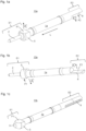
- the Figure 1 shows a schematic drawing of a contact element 10a according to a preferred embodiment of the present invention in a perspective view.
- the contact element 10a is designed for use in a plug connector and has a cylindrical conductive contact element body 1.
- At least one adaptation element or an adaptation structure 5 is formed on the contact element body 1 at a first end section E1 of the contact element 10a.
- this adaptation structure 5 represents a local thickening and/or casing of the contact element body 1.
- the adaptation structure 5 is designed and provided electrical properties of the contact element 10a and/or a plug connector in which the contact element can be arranged can be adapted and/or adjusted by modifying the adaptation structure 5.
- the adaptation structure 5 of the contact element 10a has already been modified.
- material was removed from a radial side of the cylindrical or annular adaptation structure 5 in such a way that a substantially flat surface F1 was formed.
- the contact element 10a also has a contact pin or contact pin 2, which is inserted into a complementary socket 6 (see Figure 1c ) can be introduced to establish an electrical connection with another contact element 10b (see Figure 1c ).
- the adaptation structure 5 is formed directly on the contact pin 2 of the contact element 10a.
- the contact pin 2 is designed as a tapered end portion of the contact element body 1a and has a contact tip at its axial end.
- a soldering connection or a soldering contour 8 for soldering an electrical conductor to the conductive contact element body 1a.
- the solder connection 8 is formed as a flat surface (or surface) F2 of the contact element body 1a.
- the axial end section E2 of the contact element body 1a is flattened so that it has a substantially flat surface (or surface) for placing and soldering an electrical conductor.
- the flat surface F2 of the solder connection 8 can also be produced by material removal, in particular by milling, grinding, cutting, butting and/or by laser ablation of the end section E2 of the contact element body 1a.
- An electrical conductor such as a strand of a cable, can be soldered to the flat surface F2 of the second end section E2 using solder, thereby creating a mechanical and electrical connection between the electrical conductor and the contact element 10a.
- the axial soldering end section E2 of the contact element 10a has the shape and/or geometry of a solid half cylinder (or flattened solid cylinder).
- An electrical conductor can thus be placed and soldered onto the axial end section E2 coming from a variety of directions (or from several sides, for example from the front, from the right and/or from the left).
- a flat soldering surface significantly facilitates the soldering of a corresponding number of electrical conductors or strands, particularly in the case of a plug connector which has a large number of contact elements 10a.
- the contact element 10a or the contact element body 1a has an adaptation structure 5 with a first flat surface F1 and a soldering contour or a soldering connection 8 with a second flat surface F2.
- the first flat surface F1 is formed on the first axial end section E1 of the contact element 10a or contact element body 1a, while the second flat surface F2 is formed on the second axial end section E2.
- Both flat surfaces F1 and F2 extend parallel to a longitudinal axis L of the contact element body 1a.
- the first flat surface F1 and the second flat surface F2 are formed on opposite radial sides of the cylindrical contact element body 1a, ie the first flat surface F1 faces away from the second flat surface F2.
- the flat surfaces F1 and F2 are arranged and / or designed in such a way that a normal vector or a direction R1 _ the first flat surface F1 opposite to a normal vector or a direction R2 _ the second flat surface F2 is aligned.
- such a configuration has the advantage that when two contact elements 10a are arranged in parallel (as for example in the Figure 2a shown) electrical properties of the contact elements 10a or the pair of contact elements can be adjusted by means of the adaptation structures 5 on the first axial end sections E1 of the contact elements 10a, while at the second end sections E2 of the contact elements 10a, regardless of or despite the soldering of strands of one or more cables, a very specific predefined distance D (see also Figure 6b ) between the second end sections E2 of the contact elements 10a can be maintained.
- this distance D is not influenced by the application of solder.
- the Figure 1c shows a schematic drawing of an exemplary contact element 10b, which can be electrically and mechanically connected to the contact element 10a according to the invention.
- the end section E2 of the contact element body 1b of the contact element 10b is not designed as a solder connection, but as a socket 6.
- the contact element body 1b has an opening or a slot.
- the contact element 10 also has a contact pin 3, which is formed by the adaptation structure 5 or is integrated into it.
- the contact pin 3 is used to electrically contact contacts on a circuit board.
- the contact elements 10b can be soldered to the circuit board using the contact pins 3, in particular by SMD soldering.
- the adaptation structure 5 is designed such that the size A of a flat surface F1 resulting from material removal (eg milling or cutting) from the adaptation structure 5 depends on a removal depth.
- the size of the area F1 can thus be determined by the amount of material that is removed from the adaptation structure.
- the surface F1 and thus also electrical properties of the contact element such as a capacitance or an impedance, in particular in connection with at least one further contact element arranged parallel to the contact element, can be adapted and/or adjusted.
- the Figure 2a shows a schematic drawing of an exemplary contact element system 50 (here, for example, a "SuperSpeed transmitter differential pair" for a "USB 3.1 - Socket and Plug” circular connector).
- the contact element system 50 of Figure 2a comprises two contact elements 10b arranged parallel to one another, which can be arranged in particular in a base element (here the female part) of a plug connector, and two contact elements 10a arranged parallel to one another, which can be arranged in particular in a plug element (ie the male part) of the plug connector.
- the contact pins 2 of the plug contact elements 10a are inserted into the sockets 6 of the socket contact elements 10b.
- An electrical conductor or a strand 13 of a cable 18 is soldered to the flat surfaces of the soldering end sections E2 of the plug contact elements 10a.
- the two contact elements 10a are arranged parallel to one another in such a way that the first flat surfaces F1 of the adaptation structures 5 face each other, while the second flat surfaces F2 (ie the flat surfaces of the solder connections formed by the end sections E2) the two contact elements 10a face away from each other.
- the Figure 2b shows an enlarged section of the adaptation structures 5 of the socket contact element pair (comprising two socket contact elements 10b arranged parallel to one another) of the contact element system 50 from Figure 2a .
- the Figure 2c shows an enlarged section of the adaptation structures 5 of the plug contact element pair (comprising two plug contact elements 10a arranged parallel to one another) of the contact element system 50 from Figure 2a .
- the flat surfaces F1 of the modified adaptation structures 5 are spaced apart by a distance d.
- the Figure 2d shows a waveguide equivalent circuit diagram for a pair of contact elements arranged in parallel or one above the other, as in each case Figures 2a to 2c exemplary shown.
- the contact element pair can be, for example, a differential contact element pair.
- Z L ′ C ′ .
- the impedance Z is therefore dependent on the capacitance or the capacitance C' at a constant L'.
- the capacity of a pair of contact elements can be adjusted in particular via the size A of the area F1.
- the following applies to the capacity C: C ⁇ ⁇ A d
- the capacity therefore depends on the size A of the area F1 and the distance d.
- the size A can be adjusted by modifying the adaptation structure 5 of the contact elements 10a and 10b.
- the capacity C can be adjusted by modifying the adaptation structure 5 of the contact elements 10a or 10b. In particular, the capacity C can be increased by flattening the adaptation structure 5 and thus increasing the area F1 or A.
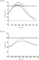
- a particular challenge with connectors is to achieve the most constant impedance possible, which is at least within certain tolerance limits.
- a desired or permissible impedance range can be between 80 ⁇ and 100 ⁇ .
- a measurement result of the impedance as a function of time for differential standard contact element pairs without matching structures is shown, while in the Figure 3b the corresponding measurement result for differential contact element pairs with adaptation structures according to the invention is shown.
- the measured impedances of the standard contact element pairs are sometimes outside the tolerance limits specified above (see the diagram of Figure 3a ), while the measured impedances for the contact element pairs with modified matching structures and thus adapted or optimally set capacitances lie within the tolerance limits specified above (see the diagram of Figure 3b ).
- the Figure 4a shows a schematic drawing of a further exemplary contact element system 50.
- the contact element system 50 comprises a first contact element system 50a and a second contact element system 50b.
- the contact element system 50a comprises a plurality of contact elements 10a (see also the Figures 1a and 1b ), while the contact element system 50b has a plurality of contact elements 10b (see also the Figure 1c ).
- a corresponding number of cables 18 are guided through a cable guide element 16, and the strands of these cables are soldered to the solder connections 8 of the contact elements 10a.
- the contact pins 2 of the contact elements 10a are inserted or plugged into the sockets 6 of the contact elements 10b.
- the Figure 4b shows a schematic drawing of the contact element system 50 from Figure 4a , wherein the plug contact elements 10b are at least partially formed by one Plug insulating element 20 are surrounded.
- a corresponding socket insulating element in the Figure 4b not shown) in particular also surrounds the socket contact elements 10a.
- a socket insulating element is in the Figure 4b however omitted.
- the Figure 5 shows a schematic drawing of a connector 100 according to an exemplary embodiment of the present invention in a perspective side view.
- the connector 100 which in the embodiment shown represents a circular connector (in particular a USB 3.1 circular connector), includes, as in the Figures 4a and 4b shown, a contact element system 50 with a plurality of contact elements 10a (in Figure 5 not recognizable) and 10b.
- the connector 100 has a connector plug 30 with a first contact element system 50a, the contact elements 10a (in Figure 5 not recognizable) each has a contact pin 2, which can be inserted into one of the contact sockets 6 (see in particular the Figures 1a to 1c ).
- the plug connector 100 has a plug connector base 40 with a second contact element system 50b, the contact elements 10b of which each have a contact socket 6 for receiving one of the contact pins 2 of the contact elements 10a.
- This in Figure 5 Element 30 shown represents a connector plug or a plug housing, while the element 40 represents a connector socket or a socket housing.
- the connector plug has a plug contact element system 50a with a plurality of contact elements 10a, a plug insulating element 20 for insulating the plug contact elements 10a, and a plug housing 30 which contains the plug insulating element 20 and thus also the plug contact elements 10a surrounds.
- the connector base has a base contact element system 50b with a plurality of base contact elements 10b, a base insulating element for insulating the base contact elements 10b, and a Base housing 40, which surrounds the base insulating element and thus also the base contact elements 10b.
- the connector base 40 also has four drilling or screw holes in order to attach the connector base to a circuit board (not shown in the figures) with screws, preferably in such a way that the base contact elements 10b with associated contacts the circuit board are electrically connected.
- the Figure 6a shows a schematic drawing of the connector 100 from Figure 5 in a front view.
- the connector 100 or the contact element system 50 arranged in the connector 100 includes both unmodified contact elements (ie contact elements without an adaptation structure and/or contact elements with an unmodified adaptation structure) and modified contact elements (ie contact elements with a modified adaptation structure).
- the contact element system 50 includes at least two differently modified contact elements.
- the contact element system 50 as in the Figure 6a shown include four unmodified contact elements (each without an adaptation structure) and six contact elements, each with a modified adaptation structure.
- the contact element system 50 it would also be possible for the contact element system 50 to include at least two contact elements with differently modified adaptation structures.
- Two contact elements 10b arranged one above the other or next to one another, each of which has a modified adaptation structure form a differential contact element pair 15 (“differential pair”).
- the connector or the contact element system 50 comprises four unmodified contact elements (each of which have no adaptation structure), and six modified contact elements, each with a modified adaptation structure.
- the modified adaptation structures of the six modified contact elements each have a flat surface.
- the six modified contact elements include three contact element pairs 15 (in particular "Differential pairs") each with two modified contact elements, the two modified contact elements of each contact element pair 15 being arranged parallel to one another in such a way that the flat surfaces of the adaptation structures of the two modified contact elements of each contact element pair 15 face each other.
- Two modified contact elements of a first contact element pair of the three contact element pairs are also arranged rotated by 90° relative to each of the remaining modified contact elements of the other two contact element pairs with respect to the flat surfaces.
- the four unmodified contact elements viewed in a section perpendicular to the longitudinal axes of the unmodified contact elements, are arranged at the corners of a rectangle.
- the four unmodified contact elements are arranged such that their axial end sections E1 (see, for example, Figure 1c ) form the corners of a rectangle.
- the Figure 6b shows a schematic drawing of a section of the connector from Figure 5 in a perspective rear view.
- the end sections E2 or the solder connections 8 of the plug contact elements 10a see also the Figures 1a and 1b .
- the Figure 6b Only two of the ten connected cables 18 are shown, while the remaining eight cables are hidden.
- the two modified contact elements 10a of each pair of contact elements 15 each have a predetermined distance D at the end sections E2 or the solder connections 8.
- the contact elements 10a By arranging the contact elements 10a in such a way that in the contact element pairs 15 the flat soldering surfaces 8 of the two contact elements involved are facing away from each other, it can advantageously be ensured that the distance D always remains the same regardless of the solder introduced when soldering the strands. This advantageously ensures electrical properties that are as constant as possible, such as, for example, a capacitance and/or impedance of the plug connector 100 or the contact element system 50 arranged in the plug connector 100 that is as constant as possible.
Landscapes
- Coupling Device And Connection With Printed Circuit (AREA)
Abstract
Description
- Die Erfindung betrifft ein Kontaktelement für einen Steckverbinder, ein Kontaktelementsystem und einen Steckverbinder.
- Bei einem Steckverbinder, dessen Kontaktelemente mit elektrischen Leitern bzw. Litzen eines oder mehrerer Kabel verlötet werden müssen, ist es wünschenswert, dass das Anlöten der elektrischen Leiter an die Kontaktelemente möglichst einfach, zuverlässig und reproduzierbar erfolgen kann. Dies trifft insbesondere bei Steckverbindern mit einer Vielzahl von Kontaktelementen und einer entsprechenden Vielzahl von anzulötenden Kabeln, welche zudem auch noch miteinander verdrillt sind, zu. Zudem ist es wünschenswert, dass das Anlöten der elektrischen Leiter an die Kontaktelemente des Steckverbinders möglichst wenig Einfluss auf die elektrischen Eigenschaften des Kontaktelements und/oder des Steckverbinders hat.
- Es ist daher eine Aufgabe der vorliegenden Erfindung, ein verbessertes Kontaktelement für einen Steckverbinder, sowie einen diesbezüglichen Steckverbinder bereitzustellen. Diese Aufgabe wird durch die Gegenstände der nebengeordneten Ansprüche gelöst. Vorteilhafte Ausführungsformen sind Gegenstand der Unteransprüche.
- Ein erster unabhängiger Aspekt zur Lösung der Aufgabe betrifft ein Kontaktelement für einen Steckverbinder, umfassend einen leitfähigen zylindrischen Kontaktelementkörper, wobei ein axialer Endabschnitt des Kontaktelementkörpers abgeflacht ist und eine im Wesentlichen ebene Fläche (bzw. Oberfläche) zum Anlöten eines elektrischen Leiters aufweist.
- Als Kontaktelement wird im Rahmen dieser Erfindung insbesondere ein elektrischer Leiter verstanden, welcher Bestandteil eines Steckverbinders, insbesondere eines Steckverbinder-Sockels oder eines Steckverbinder-Steckers, ist. Das Kontaktelement ist ausgelegt, um elektrische Signale zu übertragen, z.B. von einem Kabel zu einem weiteren Steckverbinder und/oder zu einer Leiterplatte und/oder umgekehrt. Vorzugsweise ist der Kontaktelementkörper massiv, insbesondere als massiver Zylinder, ausgebildet. Der Kontaktelementkörper kann aus einem Metall oder einer Metalllegierung gebildet sein. Vorzugsweise weist der Kontaktelementkörper Kupfer und/oder eine oder mehrere Kupferlegierungen, insbesondere Kupfer-Beryllium (CuBe), Bronze (CuSn) und/oder Messing (CuZn), auf bzw. ist aus einem oder mehreren dieser Materialien gefertigt. Es versteht sich, dass grundsätzlich auch beliebig andere Materialien, die sich für eine Signalübertragung eignen, wie z.B. Silber und/oder Gold, zur Ausbildung des Kontaktelementkörpers verwendet werden können.
- Die ebene Fläche (bzw. Oberfläche) stellt insbesondere eine Lötfläche bzw. einen Lötanschluss dar. Somit weist das Kontaktelement insbesondere einen Lötanschluss (hierin auch als Lötkontur oder Lötfläche bezeichnet) auf, welcher als eine ebene Fläche (bzw. Oberfläche) des Kontaktelementkörpers ausgebildet ist.
- Unter einer "ebenen Fläche bzw. Oberfläche" wird insbesondere eine Fläche bzw. Oberfläche verstanden, für die gilt, dass zu je zwei Punkten der Fläche bzw. Oberfläche auch eine durch diese zwei Punkte verlaufende Strecke vollständig in der Fläche bzw. Oberfläche liegt. Die ebene Fläche kann z.B. durch ein Abfräsen des Endabschnitts des Kontaktelementkörpers erzeugt werden, weshalb die ebene Fläche in diesem Fall auch als "abgefräste Fläche" bzw. "abgefräste Oberfläche" bezeichnet werden kann. Es versteht sich, dass die ebene Fläche jedoch alternativ auch durch andere Methoden, wie z.B. durch ein Abschleifen, Schneiden (insbesondere mit einem Sägeblatt), Stoßen, und/oder mittels Laserablation, erzeugt werden kann.
- Der elektrische Leiter (z.B. die Litze eines Kabels) ist insbesondere mit Hilfe von Lötzinn auf der ebenen Oberfläche des (Löt)-Endabschnitts bzw. Lötanschlusses anlötbar.
- Im Rahmen der vorliegenden Erfindung wurde erkannt, dass ein derart ausgebildeter Lötanschluss im Vergleich zu einem konventionellen Lötkelch vor allem den Vorteil bietet, dass bei einer Vielzahl von parallel zueinander angeordneten Kontaktelementen ein Kabel, dessen Litzen jeweils an die Kontaktelemente angelötet werden sollen, möglichst lange oder möglichst weit, d.h. bis auf einen kleinen Endabschnitt des Kabels, verdrillt bleiben kann. Zudem ist es für das Anlöten des Kabels ausreichend, nur ein kleines Stück der Litze des Kabels freizulegen bzw. den Kabelschirm nur an einen kleinen Endabschnitt des Kabels zu entfernen. Insbesondere müssen die Leiter bzw. Litzen des Kabels nicht wie bei einem konventionellen Lötkelch aus einer ganz bestimmten Richtung in einen Hohlzylinder eingeführt werden, sondern können (beispielsweise von oben oder auch seitlich, insbesondere paarweise) an den Lötanschluss bzw. die Lötfläche herangeführt werden. Dies erleichtert wesentlich das Anlöten von elektrischen Leitern bzw. Litzen eines oder mehrerer Kabel an die Kontaktelemente.
- In einer bevorzugten Ausführungsform ist der axiale Endabschnitt (bzw. Löt-Endabschnitt) als ein massiver Halbzylinder (bzw. als ein abgeflachter massiver Zylinder) ausgebildet. Mit anderen Worten ist der axiale Endabschnitt (bzw. Löt-Endabschnitt) zu einem massiven Halbzylinder und/oder einem abgeflachten massiven Zylinder geformt.
- In einer weiteren bevorzugten Ausführungsform ist der axiale (Löt)-Endabschnitt des Kontaktelementkörpers derart abgeflacht, dass ein elektrischer Leiter aus einer Vielzahl von Richtungen kommend (bzw. von mehreren Seiten kommend, also z.B. von vorne, von rechts und/oder von links) auf den axialen Endabschnitt zum Anlöten gelegt werden kann. Der Lötanschluss unterscheidet sich insbesondere von einem konventionellen Lötkelch, welcher einen Hohlzylinder umfasst, in den der elektrische Leiter zum Anlöten von oben eingeführt werden muss.
- In einer weiteren bevorzugten Ausführungsform weist der Kontaktelementkörper zumindest eine Anpassungsstruktur auf, welche ausgelegt und vorgesehen ist, elektrische Eigenschaften des Kontaktelements und/oder des Steckverbinders durch eine Modifikation der Anpassungsstruktur anzupassen und/oder einzustellen. Vorzugsweise ist die Anpassungsstruktur an einem ersten axialen Endabschnitt des Kontaktelements bzw. Kontaktelementkörpers ausgebildet ist, während die ebene Fläche zum Anlöten eines elektrischen Leiters an einem zweiten axialen Endabschnitt des Kontaktelements bzw. Kontaktelementkörpers ausgebildet ist. Dabei unterscheidet sich der erste axiale Endabschnitt vom zweiten axialen Endabschnitt.
- Die modifizierbare Anpassungsstruktur (auch als Anpassungselement bezeichnet) ist ausgelegt, um elektrische Eigenschaften des Kontaktelements, insbesondere bezüglich eines oder mehreren weiteren Kontaktelementen (welches/welche insbesondere in einem definierten und/oder vorgegebenen Abstand, vorzugsweise parallel bzw. übereinander, zum besagten Kontaktelement angeordnet ist/sind), durch eine Modifikation (insbesondere eine physische und/oder geometrische Modifikation bzw. Änderung) der Anpassungsstruktur anzupassen und/oder einzustellen.
- Elektrische Eigenschaften des Kontaktelements (bzw. eines Kontaktelementpaares) können z.B. kapazitive und/oder impedantische Eigenschaften, insbesondere eine Kapazität und/oder eine Impedanz, und/oder eine Luftstrecke und/oder eine Kriechstrecke umfassen. Vorzugsweise ist die Anpassungsstruktur eine Kapazitätsanpassungsstruktur, welche ausgelegt und vorgesehen ist, kapazitive Eigenschaften bzw. eine Kapazität des Kontaktelements und/oder des Steckverbinders anzupassen und/oder einzustellen. Alternativ oder zusätzlich kann die Anpassungsstruktur eine Impedanz-Anpassungsstruktur sein, welche ausgelegt und vorgesehen ist, eine Impedanz des Kontaktelements und/oder des Steckverbinders anzupassen und/oder einzustellen.
- Mit Hilfe der Anpassungsstruktur können die elektrischen Eigenschaften des Kontaktelements und/oder des Steckverbinders, je nach Anordnung und/oder der Umgebung des Kontaktelements im Steckverbinder, vorteilhafterweise an die jeweiligen Gegebenheiten bzw. Anforderungen angepasst und/oder optimiert werden. Vorzugsweise stellt die Anpassungsstruktur eine lokale Vergrößerung bzw. lokale Verdickung des (insbesondere zylindrischen) Kontaktelementkörpers dar. Insbesondere ist die Anpassungsstruktur als eine im Wesentlichen ringförmige Struktur bzw. als ringförmiges Element ausgebildet, welche bzw. welches einen Abschnitt, insbesondere einen Endabschnitt, des Kontaktelementkörpers umgibt.
- In einer weiteren bevorzugten Ausführungsform umfasst die Modifikation der Anpassungsstruktur einen (gezielten) Materialabtrag der Anpassungsstruktur, insbesondere derart, dass durch den Materialabtrag die Anpassungsstruktur eine ebene Fläche mit einem vorgegebenen Flächeninhalt aufweist. Insbesondere ist die Anpassungsstruktur derart beschaffen, dass die Modifikation der Anpassungsstruktur (gezielt) durch einen Materialabtrag der Anpassungsstruktur erfolgen kann. Der Materialabtrag kann insbesondere durch eine spanende Bearbeitung erfolgen. Der Materialabtrag kann insbesondere durch ein Fräßen und/oder Schleifen (insbesondere Tiefschleifen) und/oder Schneiden (z.B. mit einem Sägeblatt) und/oder Stoßen und/oder durch eine Laserablation der Anpassungsstruktur erfolgen.
- In einer weiteren bevorzugten Ausführungsform ist die Anpassungsstruktur derart ausgebildet (und/oder geformt), dass die Größe einer durch einen Materialabtrag der Anpassungsstruktur resultierenden ebenen Fläche von einer Abtragungstiefe abhängt.
- Vorzugsweise ist die Anpassungsstruktur an einem axialen Endabschnitt bzw. einem axialen Ende des Kontaktelementkörpers ausgebildet.
- In einer weiteren bevorzugten Ausführungsform ist die Anpassungsstruktur an einem Kontakt-Pin des Kontaktelementkörpers ausgebildet. Insbesondere kann die Anpassungsstruktur als Kontakt-Pin (auch als Kontaktstift bezeichnet) ausgebildet oder zu einem Kontakt-Pin geformt sein. Der Kontakt-Pin ist insbesondere ausgelegt, um in eine komplementäre Kontakt-Buchse (insbesondere eines weiblichen Kontaktelements) eingeführt zu werden. Mit anderen Worten kann die Anpassungsstruktur einen Kontakt-Pin zum Einführen in eine Kontakt-Buchse darstellen. Die Anpassungsstruktur weist somit vorzugsweise nicht nur eine modifizierbare Fläche bzw. Oberfläche zum Einstellen von elektrischen Eigenschaften auf, sondern stellt gleichzeitig einen Kontakt-Pin dar. Der Kontakt-Pin ist insbesondere als ein verjüngter Abschnitt, insbesondere als ein verjüngter Endabschnitt, des Kontaktelements bzw. Kontaktelementkörpers ausgebildet.
- In einer weiteren bevorzugten Ausführungsform weist die Anpassungsstruktur, insbesondere in Folge einer Modifikation (bzw. eines Materialabtrags), eine im Wesentlichen ebene Fläche (bzw. Oberfläche) auf. Die ebene Fläche erstreckt sich vorzugsweise parallel zu einer Längsachse des Kontaktelements bzw. Kontaktelementkörpers. Mit anderen Worten ist ein Normalenvektor der ebenen Fläche vorzugsweise orthogonal zur Längsachse des Kontaktelements bzw. Kontaktelementkörpers ausgerichtet. Dabei wird auch hier unter einer "ebenen Fläche bzw. Oberfläche" insbesondere eine Fläche bzw. Oberfläche verstanden, für die gilt, dass zu je zwei Punkten der Fläche bzw. Oberfläche auch eine durch diese zwei Punkte verlaufende Strecke vollständig in der Fläche bzw. Oberfläche liegt.
- Vorzugsweise stellt die ebene Fläche der Anpassungsstruktur eine erste ebene Fläche dar, während die ebene Fläche zum Anlöten eines elektrischen Leiters eine zweite ebene Fläche des Kontaktelements bzw. Kontaktelementkörpers darstellt. Vorzugsweise sind die erste ebene Fläche und die zweite ebene Fläche auf jeweils gegenüberliegenden radialen Seiten des Kontaktelementkörpers ausgebildet.
- Das Kontaktelement bzw. der Kontaktelementkörper weist somit in einer bevorzugten Ausführungsform eine Anpassungsstruktur mit einer ersten ebenen Fläche (bzw. Oberfläche) und einen Lötanschluss (bzw. eine Lötkontur) mit einer zweiten ebenen Fläche (bzw. Oberfläche) auf. Vorzugsweise ist die erste ebene Fläche (d.h. die ebene Fläche der Anpassungsstruktur) an einem ersten axialen Endabschnitt des Kontaktelements bzw. Kontaktelementkörpers ausgebildet, während die zweite ebene Fläche (d.h. die ebene Fläche des Lötanschlusses) an dem zweiten axialen Endabschnitt ausgebildet ist. Vorzugsweise ist die erste ebene Fläche an einem ersten radialen Endabschnitt des Kontaktelements bzw. Kontaktelementkörpers ausgebildet, während die zweite ebene Fläche an einem zweiten radialen Endabschnitt des Kontaktelements bzw. Kontaktelementkörpers, der dem ersten radialen Endabschnitt gegenüberliegt, ausgebildet. Mit anderen Worten sind die erste ebene Fläche und die zweite ebene Fläche auf jeweils unterschiedlichen, insbesondere gegenüberliegenden, radialen Seiten des zylindrischen Kontaktelements bzw. Kontaktelementkörpers ausgebildet. Mit anderen Worten sind die die erste ebene Fläche bzw. Oberfläche und die zweite ebene Fläche bzw. Oberfläche voneinander abgewandt. Insbesondere sind die erste ebene Fläche (der Anpassungsstruktur) und die zweite ebene Fläche (des Lötanschlusses) derart ausgebildet und/oder angeordnet, dass ein Normalenvektor der ersten ebenen Fläche bzw. Oberfläche entgegengesetzt zu einem Normalenvektor der zweiten ebenen Fläche bzw. Oberfläche ausgerichtet ist. Dies hat den Vorteil, dass bei einem parallelen Anordnen zweier solcher Kontaktelemente, z.B. zu einem "Differential-Kontaktelementpaar" (engl. "differential pair"), mittels der Anpassungsstrukturen an den ersten axialen Endabschnitten der Kontaktelemente elektrische Eigenschaften der Kontaktelemente bzw. des Kontaktelementpaares eingestellt werden können, während an den zweiten Endabschnitten der Kontaktelemente unabhängig vom (bzw. trotz dem) Anlöten von Litzen eines oder mehrerer Kabel ein ganz bestimmter vordefinierter Abstand zwischen den zweiten Endabschnitten der Kontaktelemente gewährleistet werden kann. Vorzugsweise sind daher, insbesondere in einem montierten bzw. zusammengesteckten Zustand des Steckverbinders, zwei Kontaktelemente (z.B. eines Differential-Kontaktelementpaares) derart parallel zueinander angeordnet, dass die ersten ebenen Flächen (d.h. die ebenen Flächen der Anpassungsstrukturen) der beiden Kontaktelemente einander zugewandt und die zweiten ebenen Flächen (d.h. die ebenen Flächen der Lötanschlüsse) der beiden Kontaktelemente voneinander abgewandt sind.
- Ein weiterer unabhängiger Aspekt zur Lösung der Aufgabe betrifft ein Kontaktelementsystem (insbesondere ein Kontaktelementpaar) für einen Steckverbinder, umfassend zumindest ein erstes und zweites erfindungsgemäßes Kontaktelement, wobei das erste und zweite Kontaktelement derart parallel zueinander (insbesondere übereinander) angeordnet sind, dass die jeweiligen ebenen Flächen zum Anlöten eines elektrischen Leiters voneinander abgewandt sind.
- Insbesondere könnten die Kontaktelemente des Kontaktelementsystems jeweils zumindest eine Anpassungsstruktur aufweisen. Auf diese Weise können elektrische Eigenschaften (z.B. kapazitive und/oder impedantische Eigenschaften, insbesondere eine Kapazität und/oder eine Impedanz), welche bei einer parallelen Anordnung des ersten und zweiten Kontaktelements zueinander vorliegen, angepasst und/oder eingestellt werden. Insbesondere können die elektrischen Eigenschaften, welche bei einem bestimmten bzw. vorgegebenen Abstand der parallel zueinander bzw. übereinander angeordneten ersten und zweiten Kontaktelemente vorliegen, angepasst und/oder eingestellt werden.
- Insbesondere kann die Anpassungsstruktur zumindest eines der Kontaktelemente des Kontaktelementsystems (vorzugsweise die Anpassungsstrukturen von zumindest zwei Kontaktelementen des Kontaktelementsystems) zur Anpassung der elektrischen Eigenschaften des Kontaktelementsystems und/oder des Steckverbinders modifiziert (insbesondere geometrisch verändert, wie z.B. gefräst oder geschnitten) worden sein.
- In einer bevorzugten Ausführungsform weist die Anpassungsstruktur des ersten Kontaktelements und die Anpassungsstruktur des zweiten Kontaktelements jeweils eine im Wesentlichen ebene Fläche (bzw. Oberfläche) auf. Insbesondere wurde die Anpassungsstruktur des ersten Kontaktelements und die Anpassungsstruktur des zweiten Kontaktelements derart modifiziert, dass sie jeweils eine im Wesentlichen ebene Fläche (bzw. Oberfläche) aufweisen. Das erste Kontaktelement und das zweite Kontaktelement (bzw. die jeweiligen Kontaktelementkörper) sind vorzugsweise derart parallel zueinander (und/oder übereinander) angeordnet, dass die ebene Fläche der Anpassungsstruktur des ersten Kontaktelements und die ebene Fläche der Anpassungsstruktur des zweiten Kontaktelements einander zugewandt sind.
- Das Kontaktelementsystem kann zumindest ein unmodifiziertes Kontaktelement (z.B. ohne Anpassungsstruktur oder mit einer unmodifizierten Anpassungsstruktur) und zumindest ein modifiziertes Kontaktelement (mit einer modifizierten Anpassungsstruktur) umfassen. Alternativ oder zusätzlich kann das Kontaktelementsystem zumindest zwei unterschiedlich modifizierte Kontaktelemente umfassen. Beispielsweise kann das Kontaktelementsystem zumindest ein unmodifiziertes Kontaktelement ohne Anpassungsstruktur und zumindest ein Kontaktelement mit einer modifizierten Anpassungsstruktur umfassen. Es ist aber auch möglich, dass das Kontaktelementsystem zumindest zwei Kontaktelemente mit unterschiedlich modifizierten Anpassungsstrukturen umfasst. Insbesondere wird im Rahmen der Erfindung unter einem "unmodifizierten Kontaktelement" ein Kontaktelement ohne Anpassungsstruktur oder ein Kontaktelement mit einer unmodifizierten Anpassungsstruktur verstanden. Unter einem "modifizierten Kontaktelement" wird insbesondere ein Kontaktelement mit einer modifizierten Anpassungsstruktur verstanden.
- Insbesondere kann das Kontaktelementsystem vier unmodifizierte Kontaktelemente (z.B. jeweils ohne eine Anpassungsstruktur, oder mit jeweils einer unmodifizierten Anpassungsstruktur, oder eine Kombination aus einem oder mehreren Kontaktelementen ohne Anpassungsstruktur und einem oder mehreren Kontaktelementen mit einer unmodifizierten Anpassungsstruktur) und sechs modifizierte Kontaktelemente (mit jeweils einer modifizierten Anpassungsstruktur) umfassen. Die modifizierten Anpassungsstrukturen der sechs modifizierten Kontaktelemente können jeweils eine im Wesentlichen ebene Fläche (bzw. Oberfläche) aufweisen. Insbesondere können die Anpassungsstrukturen der sechs modifizierten Kontaktelemente derart modifiziert worden sein, dass sie jeweils eine im Wesentlichen ebene Fläche (bzw. Oberfläche) aufweisen. Die sechs modifizierten Kontaktelemente können drei Kontaktelementpaare mit jeweils zwei modifizierten Kontaktelementen umfassen, wobei die zwei modifizierten Kontaktelemente eines jeden Kontaktelementpaares derart parallel zueinander angeordnet sind, dass die ebenen Flächen der Anpassungsstrukturen der zwei modifizierten Kontaktelemente eines jeden Kontaktelementpaares einander zugewandt sind. Vorzugsweise können zwei modifizierte Kontaktelemente eines ersten Kontaktelementpaares der drei Kontaktelementpaare relativ zu jedem der übrigen modifizierten Kontaktelemente der anderen beiden Kontaktelementpaare bezüglich der ebenen Flächen um 90° gedreht angeordnet sein. Mit anderen Worten können die Kontaktelemente der drei Kontaktelementpaare vorzugsweise derart angeordnet sein, dass ein Normalenvektor der zwei modifizierten Kontaktelemente eines ersten Kontaktelementpaares der drei Kontaktelementpaare senkrecht zu den Normalenvektoren sämtlicher der übrigen modifizierten Kontaktelemente der anderen beiden Kontaktelementpaare ausgerichtet ist.
- Die vier unmodifizierten Kontaktelemente können insbesondere, betrachtet in einem Schnitt senkrecht zu den Längsachsen der Kontaktelemente (bzw. bezüglich einer Schnittebene senkrecht zu den Längsachsen der Kontaktelemente), an den Ecken eines Rechtecks angeordnet sein. Insbesondere können die vier unmodifizierten Kontaktelemente derart angeordnet sein, dass deren axialen Endabschnitte bzw. Endpunkte (und/oder, sofern vorhanden, deren Anpassungsstrukturen) die Ecken eines Rechtecks bilden. Mit anderen Worten können die vier unmodifizierten Kontaktelemente derart angeordnet sein, dass eine virtuelle Verbindungslinie, welche jeweils ein erstes axiales Ende und/oder einen ersten axialen Endabschnitt und/oder einen ersten axialen Endpunkt (und/oder insbesondere, sofern vorhanden, die Anpassungsstrukturen) der unmodifizierten Kontaktelemente miteinander verbindet, im Wesentlichen ein Rechteck bildet. Mit anderen Worten können die vier unmodifizierten Kontaktelemente (bzw. deren axialen Enden und insbesondere deren Anpassungsstrukturen) in einem Rechteck bzw. an den Ecken eines Rechtecks angeordnet sein.
- Ein weiterer unabhängiger Aspekt zur Lösung der Aufgabe betrifft einen Steckverbinder, insbesondere einen Rundsteckverbinder bzw. einen USB 3.1 Rundsteckverbinder, umfassend:
- zumindest ein erfindungsgemäßes Kontaktelement; und/oder
- zumindest ein erfindungsgemäßes Kontaktelementsystem.
- Es versteht sich, dass die vorstehend genannten und die nachfolgend noch zu erläuternden Merkmale nicht nur in der jeweils angegebenen Kombination, sondern auch in Alleinstellung oder in anderen Kombinationen verwendbar sind, ohne den Rahmen der vorliegenden Erfindung zu verlassen.
- Für die oben genannten weiteren unabhängigen Aspekte und insbesondere für diesbezügliche bevorzugte Ausführungsformen gelten auch die vor- oder nachstehend gemachten Ausführungen zu den Ausführungsformen des ersten Aspekts. Insbesondere gelten für einen unabhängigen Aspekt der vorliegenden Erfindung und für diesbezügliche bevorzugte Ausführungsformen auch die vor- und nachstehend gemachten Ausführungen zu den Ausführungsformen der jeweils anderen unabhängigen Aspekte.
- Im Folgenden werden einzelne Ausführungsformen zur Lösung der Aufgabe anhand der Figuren beispielhaft beschrieben. Dabei weisen die einzelnen beschriebenen Ausführungsformen zum Teil Merkmale auf, die nicht zwingend erforderlich sind, um den beanspruchten Gegenstand auszuführen, die aber in bestimmten Anwendungsfällen gewünschte Eigenschaften bereitstellen. So sollen auch Ausführungsformen als unter die beschriebene technische Lehre fallend offenbart angesehen werden, die nicht alle Merkmale der im Folgenden beschriebenen Ausführungsformen aufweisen. Ferner werden, um unnötige Wiederholungen zu vermeiden, bestimmte Merkmale nur in Bezug auf einzelne der im Folgenden beschriebenen Ausführungsformen erwähnt. Es wird darauf hingewiesen, dass die einzelnen Ausführungsformen daher nicht nur für sich genommen, sondern auch in einer Zusammenschau betrachtet werden sollen. Anhand dieser Zusammenschau wird der Fachmann erkennen, dass einzelne Ausführungsformen auch durch Einbeziehung von einzelnen oder mehreren Merkmalen anderer Ausführungsformen modifiziert werden können. Es wird darauf hingewiesen, dass eine systematische Kombination der einzelnen Ausführungsformen mit einzelnen oder mehreren Merkmalen, die in Bezug auf andere Ausführungsformen beschrieben werden, wünschenswert und sinnvoll sein kann und daher in Erwägung gezogen und auch als von der Beschreibung umfasst angesehen werden soll.
-
- Figur 1a
- zeigt eine schematische Zeichnung eines Kontaktelements gemäß einer bevorzugten Ausführungsform der vorliegenden Erfindung in einer perspektivischen Ansicht;
- Figur 1b
- zeigt eine schematische Zeichnung des Kontaktelements von
Figur 1 in einer weiteren perspektivischen Ansicht; - Figur 1c
- zeigt eine schematische Zeichnung eines beispielhaften Kontaktelements, welches mit dem erfindungsgemäßen Kontaktelement verbunden werden kann;
- Figur 2a
- zeigt eine schematische Zeichnung eines Kontaktelementsystems gemäß einer beispielhaften Ausführungsform der vorliegenden Erfindung;
- Figur 2b
- zeigt einen vergrößerten Ausschnitt von Anpassungsstrukturen eines ersten beispielhaften Kontaktelementpaares des Kontaktelementsystems von
Figur 2a ; - Figur 2c
- zeigt einen vergrößerten Ausschnitt von Anpassungsstrukturen eines zweiten Kontaktelementpaares des Kontaktelementsystems von
Figur 2a ; - Figur 2d
- zeigt ein Ersatzschaltbild für ein parallel angeordnetes Kontaktelementpaar;
- Figur 3a
- zeigt ein Messergebnis der Impedanz in Abhängigkeit der Zeit für differentielle Kontaktelementpaare ohne Anpassungsstrukturen;
- Figur 3b
- zeigt ein Messergebnis für die Impedanz in Abhängigkeit der Zeit für differentielle Kontaktelementpaare mit Anpassungsstrukturen;
- Figur 4a
- zeigt eine schematische Zeichnung eines Kontaktelementsystems gemäß einer weiteren beispielhaften Ausführungsform der vorliegenden Erfindung;
- Figur 4b
- zeigt eine schematische Zeichnung des Kontaktelementsystems von
Figur 4a mit einem steckerseitigen Isolierelement; - Figur 5
- zeigt eine schematische Zeichnung eines Steckverbinders gemäß einer bevorzugten Ausführungsform der vorliegenden Erfindung in einer perspektivischen Seitenansicht;
- Figur 6a
- zeigt eine schematische Zeichnung des Steckverbinders von
Figur 5 in einer Vorderansicht; - Figur 6b
- zeigt eine schematische Zeichnung eines Ausschnitts des Steckverbinders von
Figur 5 in einer perspektivischen Rückansicht. - Die in der vorliegenden Beschreibung gewählten Lageangaben, wie z. B. oben, unten, seitlich usw. sind jeweils auf die unmittelbar beschriebene sowie dargestellte Figur bezogen und sind bei einer Lageänderung sinngemäß auf die neue Lage zu übertragen.
- Die
Figur 1 zeigt eine schematische Zeichnung eines Kontaktelements 10a gemäß einer bevorzugten Ausführungsform der vorliegenden Erfindung in einer perspektivischen Ansicht. Das Kontaktelement 10a ist für den Einsatz in einem Steckverbinder ausgelegt und weist einen zylinderförmigen leitfähigen Kontaktelementkörper 1 auf. An einem ersten Endabschnitt E1 des Kontaktelements 10a ist am Kontaktelementkörper 1 zumindest ein Anpassungselement bzw. eine Anpassungsstruktur 5 ausgebildet. Wie in derFigur 1 ersichtlich, stellt diese Anpassungsstruktur 5 eine lokale Verdickung und/oder Ummantelung des Kontaktelementkörpers 1 dar. Die Anpassungsstruktur 5 ist ausgelegt und vorgesehen, elektrische Eigenschaften des Kontaktelements 10a und/oder eines Steckverbinders, in dem das Kontaktelement angeordnet werden kann, durch eine Modifikation der Anpassungsstruktur 5 anzupassen und/oder einzustellen. - Im gezeigten Beispiel der
Figur 1a wurde die Anpassungsstruktur 5 des Kontaktelements 10a bereits modifiziert. Dazu wurde an einer radialen Seite der zylindrischen bzw. ringförmigen Anpassungsstruktur 5 Material abgetragen, und zwar derart, dass sich eine im Wesentlichen ebene Fläche F1 ausgebildet hat. - Am axialen Endabschnitt E1 weist das Kontaktelement 10a ferner einen Kontaktstift bzw. Kontakt-Pin 2 auf, welcher in eine komplementäre Buchse 6 (siehe
Figur 1c ) eingeführt werden kann, um eine elektrische Verbindung mit einem weiteren Kontaktelement 10b (sieheFigur 1c ) herzustellen. Wie inFigur 1a zu sehen, ist die Anpassungsstruktur 5 unmittelbar am Kontakt-Pin 2 des Kontaktelements 10a ausgebildet. Der Kontakt-Pin 2 ist als ein verjüngter Endabschnitt des Kontaktelementkörpers 1a ausgebildet und weist an seinem axialen Ende eine Kontaktspitze auf. - An einem zweiten axialen Endabschnitt E2 (im Rahmen dieser Beschreibung auch als Löt-Endabschnitt bezeichnet) des Kontaktelements 10a ist ein Lötanschluss bzw. eine Lötkontur 8 zum Anlöten eines elektrischen Leiters an den leitfähigen Kontaktelementkörper 1a. Der Lötanschluss 8 ist als eine ebene Fläche (bzw. Oberfläche) F2 des Kontaktelementkörpers 1a ausgebildet. Wie insbesondere in der perspektivischen Ansicht der
Figur 1b erkennbar, ist hierzu der axiale Endabschnitt E2 des Kontaktelementkörpers 1a abgeflacht, so dass dieser eine im Wesentlichen ebene Fläche (bzw. Oberfläche) zum Auflegen und Anlöten eines elektrischen Leiters aufweist. Wie die ebene Fläche F1 der Anpassungsstruktur 5 kann auch die ebene Fläche F2 des Lötanschlusses 8 durch einen Materialabtrag, insbesondere durch ein Abfräsen, Abschleifen, Abschneiden, Stoßen und/oder mittels Laserablation des Endabschnitts E2 des Kontaktelementkörpers 1a erzeugt werden. - Ein elektrischer Leiter wie z.B. eine Litze eines Kabels kann mit Hilfe von Lötzinn auf der ebenen Oberfläche F2 des zweiten Endabschnitts E2 angelötet werden, um somit eine mechanische und elektrische Verbindung zwischen dem elektrischen Leiter und dem Kontaktelement 10a zu erzeugen. Der axiale Löt-Endabschnitt E2 des Kontaktelements 10a weist die Form und/oder Geometrie eines massiven Halbzylinders (bzw. abgeflachten massiven Zylinders) auf. Somit kann ein elektrischer Leiter aus einer Vielzahl von Richtungen kommend (bzw. von mehreren Seiten kommend, also z.B. von vorne, von rechts und/oder von links) auf den axialen Endabschnitt E2 gelegt und angelötet werden. Wie bereits weiter oben erläutert, erleichtert eine solche ebene Lötfläche insbesondere bei einem Steckverbinder, der eine Vielzahl von Kontaktelementen 10a aufweist, wesentlich das Verlöten einer entsprechenden Vielzahl von elektrischen Leitern bzw. Litzen.
- Wie aus den
Figuren 1a und 1b ersichtlich, weist also das Kontaktelement 10a bzw. der Kontaktelementkörper 1a eine Anpassungsstruktur 5 mit einer ersten ebenen Fläche F1 und eine Lötkontur bzw. einen Lötanschluss 8 mit einer zweiten ebenen Fläche F2 auf. Dabei ist die erste ebene Fläche F1 am ersten axialen Endabschnitt E1 des Kontaktelements 10a bzw. Kontaktelementkörpers 1a ausgebildet, während die zweite ebene Fläche F2 an dem zweiten axialen Endabschnitt E2 ausgebildet ist. Beide ebene Flächen F1 und F2 erstrecken sich parallel zu einer Längsachse L des Kontaktelementkörpers 1a. Die erste ebene Fläche F1 und die zweite ebene Fläche F2 sind auf jeweils gegenüberliegenden radialen Seiten des zylindrischen Kontaktelementkörpers 1a ausgebildet, d.h. die die erste ebene Fläche F1 ist von der zweiten ebenen Fläche F2 abgewandt. Wie in denFiguren 1a und 1b angedeutet, sind die ebenen Flächen F1 und F2 derart angeordnet und/oder ausgebildet, dass ein Normalenvektor bzw. eine RichtungR 1 der ersten ebenen Fläche F1 entgegengesetzt zu einem Normalenvektor bzw. einer RichtungR 2 der zweiten ebenen Fläche F2 ausgerichtet ist. Wie bereits weiter oben beschrieben, hat eine solche Konfiguration den Vorteil, dass bei einem parallelen Anordnen zweier Kontaktelemente 10a (wie z.B. in derFigur 2a dargestellt) mittels der Anpassungsstrukturen 5 an den ersten axialen Endabschnitten E1 der Kontaktelemente 10a elektrische Eigenschaften der Kontaktelemente 10a bzw. des Kontaktelementpaares eingestellt werden können, während an den zweiten Endabschnitten E2 der Kontaktelemente 10a unabhängig vom bzw. trotz dem Anlöten von Litzen eines oder mehrerer Kabel ein ganz bestimmter vordefinierter Abstand D (siehe auchFigur 6b ) zwischen den zweiten Endabschnitten E2 der Kontaktelemente 10a eingehalten werden kann. Denn vorteilhafterweise wird dieser Abstand D bei einer solchen Konfiguration nicht durch das Anbringen von Lötmittel beeinflusst. - Die
Figur 1c zeigt eine schematische Zeichnung eines beispielhaften Kontaktelements 10b, welches mit dem erfindungsgemäßen Kontaktelement 10a elektrisch und mechanisch verbunden werden kann. Im Vergleich zu dem in denFiguren 1a und 1b gezeigten Kontaktelementen 10a und 10b ist der Endabschnitt E2 des Kontaktelementkörpers 1b des Kontaktelements 10b nicht als Lötanschluss, sondern als Buchse 6 ausgebildet. Mit anderen Worten weist der Kontaktelementkörper 1b eine Öffnung bzw. einen Schlitz auf. Durch Einführen und/oder Einstecken des Kontakt-Pins 2 des in denFiguren 1a und 1b gezeigten Kontaktelements 10a in die Buchse 6 des Kontaktelements 10b kann eine elektrische und/oder mechanische Verbindung zwischen den Kontaktelementen 10a und 10b hergestellt werden. Das Kontaktelement 10 weist zudem einen Kontakt-Pin 3 auf, welcher durch die Anpassungsstruktur 5 ausgebildet ist bzw. in diese integriert ist. Der Kontakt-Pin 3 dient zum elektrischen Kontaktieren von Kontakten einer Leiterplatte. Insbesondere können die Kontaktelemente 10b mit Hilfe der Kontakt-Pins 3 auf die Leiterplatte, insbesondere durch ein SMD-Löten, gelötet werden. - Wie ferner aus den
Figuren 1a bis 1c ersichtlich, ist die Anpassungsstruktur 5 derart ausgebildet, dass die Größe A einer durch einen Materialabtrag (z.B. Fräsen oder Schneiden) der Anpassungsstruktur 5 resultierenden ebenen Fläche F1 von einer Abtragungstiefe abhängt. Durch die Menge des Materials, welches von der Anpassungsstruktur abgetragen wird, kann somit die Größe der Fläche F1 bestimmt werden. Auf diese Weise kann die Fläche F1 und damit auch elektrische Eigenschaften des Kontaktelements (wie z.B. eine Kapazität oder eine Impedanz), insbesondere in Verbindung mit zumindest einem zu dem Kontaktelement parallel angeordneten weiteren Kontaktelement, angepasst und/oder eingestellt werden. - Die
Figur 2a zeigt eine schematische Zeichnung eines beispielhaften Kontaktelementsystems 50 (hier z.B. ein "SuperSpeed transmitter differential pair" für einen "USB 3.1 - Socket and Plug" Rundsteckverbinder). Das Kontaktelementsystem 50 derFigur 2a umfasst zwei parallel zueinander angeordnete Kontaktelemente 10b, welche insbesondere in einem Sockelelement (hier dem weiblichen Teil) eines Steckverbinders anordenbar sind, und zwei parallel zueinander angeordnete Kontaktelemente 10a, welche insbesondere in einem Steckerelement (d.h. dem männlichen Teil) des Steckverbinders anordenbar sind. Wie in derFigur 2a dargestellt, sind jeweils die Kontakt-Pins 2 der Stecker-Kontaktelemente 10a in die Buchsen 6 der Buchsen-Kontaktelemente 10b eingesteckt. An den ebenen Flächen der Löt-Endabschnitte E2 der Stecker-Kontaktelemente 10a ist jeweils ein elektrischer Leiter bzw. eine Litze 13 eines Kabels 18 angelötet. In diesem montierten bzw. zusammengesteckten Zustand sind jeweils die zwei Kontaktelemente 10a derart parallel zueinander angeordnet, dass die ersten ebenen Flächen F1 der Anpassungsstrukturen 5 einander zugewandt sind, während die zweiten ebenen Flächen F2 (d.h. die ebenen Flächen der durch die Endabschnitte E2 ausgebildeten Lötanschlüsse) der beiden Kontaktelemente 10a voneinander abgewandt sind. - Die
Figur 2b zeigt einen vergrößerten Ausschnitt der Anpassungsstrukturen 5 des Buchsen-Kontaktelementpaares (umfassend zwei parallel zueinander angeordnete Buchsen-Kontaktelemente 10b) des Kontaktelementsystems 50 vonFigur 2a . - Die
Figur 2c zeigt einen vergrößerten Ausschnitt der Anpassungsstrukturen 5 des Stecker-Kontaktelementpaares (umfassend zwei parallel zueinander angeordnete Stecker-Kontaktelemente 10a) des Kontaktelementsystems 50 vonFigur 2a . Wie inFigur 2b angedeutet, sind jeweils die ebenen Flächen F1 der modifizierten Anpassungsstrukturen 5 mit einem Abstand d beabstandet. - Die
Figur 2d zeigt ein Wellenleiter-Ersatzschaltbild für ein parallel bzw. übereinander angeordnetes Kontaktelementpaar, wie jeweils in denFiguren 2a bis 2c beispielhaft dargestellt. Das Kontaktelementpaar kann z.B. ein differenzielles Kontaktelementpaar sein. Die Impedanz Z ergibt sich wie folgt:
- Dabei bezeichnet L' einen Induktivitätsbelag, C' einen Kapazitätsbelag, R' einen Widerstandsbelag, G' einen Querleitbelag, und ω = 2πf die Kreisfrequenz des Wechselstromes. Bei einer Frequenz ab einigen Megahertz, und somit ωL' » R' und ωC' » G', gilt vereinfacht:

- Die Impedanz Z ist somit bei konstantem L' von der Kapazität bzw. dem Kapazitätsbelag C' abhängig.
- Mit Hilfe der in den
Figuren 2b und 2c vergrößert dargestellten modifizierten Anpassungsstrukturen 5 der Kontaktelemente 10a bzw. 10b kann insbesondere über die Größe A der Fläche F1 die Kapazität eines Kontaktelementpaares eingestellt werden. Für die Kapazität C gilt dabei:
- Dabei bezeichnet ε die Dielektrizitätskonstante. Somit ist die Kapazität von der Größe A der Fläche F1 und dem Abstand d abhängig. Die Größe A kann durch eine Modifikation der Anpassungsstruktur 5 der Kontaktelemente 10a bzw. 10b eingestellt werden. Bei einem vorgegebenen Abstand d kann somit die durch eine Modifikation der Anpassungsstruktur 5 der Kontaktelemente 10a bzw. 10b die Kapazität C eingestellt werden. Insbesondere kann die Kapazität C durch ein Abflachen der Anpassungsstruktur 5, und somit einem Vergrößern der Fläche F1 bzw. A, erhöht werden.
- Eine Herausforderung bei Steckverbindern ist es insbesondere, eine möglichst konstante Impedanz, welche zumindest innerhalb von bestimmten Toleranzgrenzen liegt, zu erzielen. Beispielsweise kann ein gewünschter bzw. zulässiger Impedanzbereich zwischen 80 Ω und 100 Ω liegen. In der
Figur 3a ist ein Messergebnis der Impedanz in Abhängigkeit der Zeit für differentielle Standard-Kontaktelementpaare ohne Anpassungsstrukturen gezeigt, während in derFigur 3b das entsprechende Messergebnis für differentielle Kontaktelementpaare mit erfindungsgemäßen Anpassungsstrukturen dargestellt ist. Wie den Diagrammen entnommen werden kann, liegen die gemessenen Impedanzen bei den Standard-Kontaktelementpaaren teilweise außerhalb der oben angegebenen Toleranzgrenzen (siehe das Diagramm derFigur 3a ), während die gemessenen Impedanzen bei den Kontaktelementpaaren mit modifizierten Anpassungsstrukturen und damit angepassten bzw. optimal eingestellten Kapazitäten innerhalb der oben angegebenen Toleranzgrenzen liegen (siehe das Diagramm derFigur 3b ). Durch eine Anpassung bzw. Modifikation der erfindungsgemäßen Anpassungsstrukturen 5 kann somit eine signifikante Verbesserung der elektrischen Eigenschaften der Kontaktelemente bzw. Kontaktelementpaare erreicht werden. - Die
Figur 4a zeigt eine schematische Zeichnung eines weiteren beispielhaften Kontaktelementsystems 50. Das Kontaktelementsystem 50 umfasst ein erstes Kontaktelementsystem 50a und ein zweites Kontaktelementsystem 50b. Das Kontaktelementsystem 50a umfasst eine Vielzahl von Kontaktelementen 10a (siehe auch dieFiguren 1a und 1b ), während das Kontaktelementsystem 50b eine Vielzahl von Kontaktelementen 10b (siehe auch dieFigur 1c ) umfasst. Eine entsprechende Vielzahl von Kabeln 18 sind durch ein Kabelführungselement 16 geführt, und die Litzen dieser Kabel sind an die Lötanschlüsse 8 der Kontaktelemente 10a angelötet. Ferner sind jeweils die Kontakt-Pins 2 der Kontaktelemente 10a in die Buchsen 6 der Kontaktelemente 10b eingeführt bzw. eingesteckt. - Die
Figur 4b zeigt eine schematische Zeichnung des Kontaktelementsystems 50 vonFigur 4a , wobei die Stecker-Kontaktelemente 10b zumindest teilweise von einem Stecker-Isolierelement 20 umgeben sind. Ein entsprechendes Buchsen-Isolierelement (in derFigur 4b nicht gezeigt) umgibt insbesondere auch die Buchsen-Kontaktelemente 10a. Zur besseren Darstellbarkeit ist ein solches Buchsen-Isolierelement in derFigur 4b jedoch weggelassen. - Die
Figur 5 zeigt eine schematische Zeichnung eines Steckverbinders 100 gemäß einer beispielhaften Ausführungsform der vorliegenden Erfindung in einer perspektivischen Seitenansicht. Der Steckverbinder 100, welcher in der gezeigten Ausführungsform einen Rundsteckverbinder (insbesondere einen USB 3.1 Rundsteckverbinder) darstellt, umfasst, wie in denFiguren 4a und 4b gezeigt, ein Kontaktelementsystem 50 mit einer Vielzahl von Kontaktelementen 10a (inFigur 5 nicht erkennbar) und 10b. Dabei weist der Steckverbinder 100 einen Steckverbinder-Stecker 30 mit einem ersten Kontaktelementsystem 50a, deren Kontaktelemente 10a (inFigur 5 nicht erkennbar) jeweils einen Kontakt-Pin 2, welcher in eine der Kontaktbuchsen 6 eingeführt werden kann, auf (siehe hierzu insbesondere auch dieFiguren 1a bis 1c ). Ferner weist der Steckverbinder 100 einen Steckverbinder-Sockel 40 mit einem zweiten Kontaktelementsystem 50b auf, deren Kontaktelemente 10b jeweils eine Kontaktbuchse 6 zur Aufnahme eines der Kontakt-Pins 2 der Kontaktelemente 10a aufweisen. Das inFigur 5 dargestellte Element 30 stellt einen Steckverbinder-Stecker bzw. ein Stecker-Gehäuse dar, während das Element 40 einen Steckverbinder-Sockel bzw. ein Sockel-Gehäuse darstellt. Im montierten bzw. zusammengesteckten Zustand des Steckverbinders 100 ist jeweils ein Kontakt-Pin 2 der Kontaktelemente 10a des ersten Kontaktelementsystems in eine Kontaktbuchse 6 der Kontaktelemente 10b des zweiten Kontaktelementsystems eingeführt. - Insbesondere weist der Steckverbinder-Stecker ein Stecker-Kontaktelementsystem 50a mit einer Vielzahl von Kontaktelementen 10a, ein Stecker-Isolierelement 20 zum Isolieren der Stecker-Kontaktelemente 10a, und ein Steckergehäuse 30 auf, welches das Stecker-Isolierelement 20 und damit auch die Stecker-Kontaktelemente 10a umgibt. Entsprechend weist insbesondere der Steckverbinder-Sockel ein Sockel-Kontaktelementsystem 50b mit einer Vielzahl von Sockel-Kontaktelementen 10b, ein Sockel-Isolierelement zum Isolieren der Sockel-Kontaktelemente 10b, und ein Sockelgehäuse 40 auf, welches das Sockel-Isolierelement und damit auch die Sockel-Kontaktelemente 10b umgibt.
- Der Steckverbinder-Sockel 40 weist zudem vier Bohr- bzw. Schraublöcher auf, um den Steckverbinder-Sockel mit Schrauben an eine Leiterplatte (in den Figuren nicht gezeigt) zu befestigen, und zwar vorzugsweise derart, dass die Sockel-Kontaktelemente 10b mit zugehörigen Kontakten auf der Leiterplatte elektrisch verbunden sind.
- Die
Figur 6a zeigt eine schematische Zeichnung des Steckverbinders 100 vonFigur 5 in einer Vorderansicht. In dieser Ansicht wird deutlich, dass der Steckverbinder 100 bzw. das im Steckverbinder 100 angeordnete Kontaktelementsystem 50 sowohl unmodifizierte Kontaktelemente (d.h. Kontaktelemente ohne Anpassungsstruktur und/oder Kontaktelemente mit einer unmodifizierten Anpassungsstruktur) und modifizierte Kontaktelemente (d.h. Kontaktelemente mit einer modifizierten Anpassungsstruktur) umfasst. Insbesondere umfasst das Kontaktelementsystem 50 zumindest zwei unterschiedlich modifizierte Kontaktelemente. So kann z.B. das Kontaktelementsystem 50, wie in derFigur 6a dargestellt, vier unmodifizierte Kontaktelemente (jeweils ohne Anpassungsstruktur) und sechs Kontaktelemente mit jeweils einer modifizierten Anpassungsstruktur umfassen. Möglich wäre aber auch, dass das Kontaktelementsystem 50 zumindest zwei Kontaktelemente mit unterschiedlich modifizierten Anpassungsstrukturen umfasst. Jeweils zwei übereinander oder nebeneinander angeordnete Kontaktelemente 10b, welche jeweils eine modifizierte Anpassungsstruktur aufweise, bilden ein differenzielles Kontaktelementpaar 15 ("Differential Pair"). - Wie in der
Figur 6a erkennbar, umfasst der Steckverbinder bzw. das Kontaktelementsystem 50 vier unmodifizierte Kontaktelemente (welche jeweils keine Anpassungsstruktur aufweisen), und sechs modifizierte Kontaktelemente mit jeweils einer modifizierten Anpassungsstruktur. Die modifizierten Anpassungsstrukturen der sechs modifizierten Kontaktelemente weisen jeweils eine ebene Fläche auf. Die sechs modifizierten Kontaktelemente umfassen drei Kontaktelementpaare 15 (insbesondere "Differential Pairs") mit jeweils zwei modifizierten Kontaktelementen, wobei die zwei modifizierten Kontaktelemente eines jeden Kontaktelementpaares 15 derart parallel zueinander angeordnet sind, dass die ebenen Flächen der Anpassungsstrukturen der zwei modifizierten Kontaktelemente eines jeden Kontaktelementpaares 15 einander zugewandt sind. Zwei modifizierte Kontaktelemente eines ersten Kontaktelementpaares der drei Kontaktelementpaare sind zudem relativ zu jedem der übrigen modifizierten Kontaktelemente der anderen beiden Kontaktelementpaare bezüglich der ebenen Flächen um 90° gedreht angeordnet. Die vier unmodifizierten Kontaktelemente sind, betrachtet in einem Schnitt senkrecht zu den Längsachsen der unmodifizierten Kontaktelemente, an den Ecken eines Rechtecks angeordnet. Mit anderen Worten sind die vier unmodifizierten Kontaktelemente derart angeordnet, dass deren axialen Endabschnitte E1 (siehe z.B. dieFigur 1c ) die Ecken eines Rechtecks bilden. - Die
Figur 6b zeigt eine schematische Zeichnung eines Ausschnitts des Steckverbinders vonFigur 5 in einer perspektivischen Rückansicht. In dieser Rückansicht sind die Endabschnitte E2 bzw. die Lötanschlüsse 8 der Stecker-Kontaktelemente 10a (siehe auch dieFiguren 1a und 1b ) zu sehen. Aus Darstellungsgründen sind in derFigur 6b nur zwei der insgesamt zehn angeschlossenen Kabel 18 gezeigt, während die restlichen acht Kabel ausgeblendet sind. Somit sind vor allem die in dem Steckverbinder 100 bzw. dessen Steckelementsystem 50 derFiguren 5 ,6a und 6b vorhandenen drei Kontaktelementpaare 15, welche insbesondere differenzielle Kontaktelementpaare sind, besser erkennbar. Die zwei modifizierten Kontaktelemente 10a eines jeden Kontaktelementpaares 15 weisen an den Endabschnitten E2 bzw. den Lötanschlüssen 8 jeweils einen vorbestimmten Abstand D auf. Durch die Anordnung der Kontaktelemente 10a derart, dass bei den Kontaktelementpaaren 15 jeweils die ebenen Lötflächen 8 der zwei jeweils beteiligen Kontaktelemente voneinander abgewandt sind, kann vorteilhafterweise gewährleistet werden, dass der Abstand D unabhängig vom eingebrachten Lötzinn beim Anlöten der Litzen stets gleich bleibt. Dies gewährleistet vorteilhafterweise möglichst konstante elektrische Eigenschaften, wie z.B. eine möglichst konstante Kapazität und/oder Impedanz des Steckverbinders 100 bzw. des im Steckverbinder 100 angeordneten Kontaktelementsystems 50. -
- 1a, 1b
- Kontaktelementkörper
- 2
- Kontaktstift (Kontakt-Pin)
- 3
- Kontakt-Pin
- 5
- Anpassungselement (Anpassungsstruktur)
- 6
- Buchse
- 8
- Lötkontur (Lötanschluss)
- 10a, 10b
- Kontaktelement
- 13
- Litze (elektrischer Leiter)
- 15
- (differentielles) Kontaktelementpaar
- 16
- Kabelführelement
- 18
- Kabel
- 20
- Isolierelement
- 30
- Stecker (Gehäuse)
- 40
- Sockel (Gehäuse)
- 42
- Bohrloch (Schraubloch)
- 50
- Kontaktelementsystem
- 100
- Steckverbinder
- A
- Fläche / Flächeninhalt
- d
- Abstand
- D
- Abstand
- E1
- (erster) axialer Endabschnitt
- E2
- (zweiter) axialer Endabschnitt
- F1
- erste ebene Fläche
- F2
- zweite ebene Fläche
- L
- Längsachse
- R1
- erste Richtung
- R2
- zweite Richtung
Claims (11)
- Kontaktelement (10a) für einen Steckverbinder (100), umfassend einen leitfähigen zylindrischen Kontaktelementkörper (1a),
dadurch gekennzeichnet, dass
ein axialer Endabschnitt (E2) des Kontaktelementkörpers (1a) abgeflacht ist und eine im Wesentlichen ebene Fläche (F2) zum Anlöten eines elektrischen Leiters aufweist. - Kontaktelement (10a) nach Anspruch 1, wobei der axiale Endabschnitt (E2) als ein massiver Halbzylinder ausgebildet ist.
- Kontaktelement (10a) nach Anspruch 1 oder 2, wobei der axiale Endabschnitt (E2) des Kontaktelementkörpers (1a) derart abgeflacht ist, dass ein elektrischer Leiter aus einer Vielzahl von Richtungen kommend auf den axialen Endabschnitt (E2) zum Anlöten gelegt werden kann.
- Kontaktelement (10a) nach einem der vorangehenden Ansprüche, wobei der Kontaktelementkörper (1a) zumindest eine Anpassungsstruktur (5) aufweist, welche ausgelegt und vorgesehen ist, elektrische Eigenschaften des Kontaktelements (10a) und/oder des Steckverbinders (100) durch eine Modifikation der Anpassungsstruktur (5) anzupassen und/oder einzustellen.
- Kontaktelement (10a) nach Anspruch 4, wobei die Anpassungsstruktur (5) an einem ersten axialen Endabschnitt (E1) des Kontaktelementkörpers (1a) ausgebildet ist, während die ebene Fläche (F2) zum Anlöten eines elektrischen Leiters an einem zweiten axialen Endabschnitt (E2) des Kontaktelementkörpers (1a) ausgebildet ist, wobei sich der erste axiale Endabschnitt (E1) vom zweiten axialen Endabschnitt (E2) unterscheidet.
- Kontaktelement (10a) nach Anspruch 4 oder 5,wobei die Modifikation der Anpassungsstruktur (5) einen Materialabtrag der Anpassungsstruktur (5) umfasst, und/oderwobei die Anpassungsstruktur (5) derart ausgebildet ist, dass die Größe einer durch einen Materialabtrag der Anpassungsstruktur (5) resultierenden ebenen Fläche (F1) der Anpassungsstruktur (5) von einer Abtragungstiefe abhängt.
- Kontaktelement (10a) nach einem der Ansprüche 4 bis 6, wobei die Anpassungsstruktur (5) an einem Kontakt-Pin (3) des Kontaktelementkörpers (1a) ausgebildet ist.
- Kontaktelement (10a) nach einem der Ansprüche 4 bis 7, wobei die Anpassungsstruktur (5) eine im Wesentlichen ebene Fläche (F1) aufweist, die sich vorzugsweise parallel zu einer Längsachse (L) des Kontaktelementkörpers (1a) erstreckt.
- Kontaktelement (10a) nach Anspruch 8, wobei die ebene Fläche (F1) der Anpassungsstruktur (5) eine erste ebene Fläche darstellt, und die ebene Fläche (F2) zum Anlöten eines elektrischen Leiters eine zweite ebene Fläche des Kontaktelementkörpers (1a) darstellt, und wobei die erste ebene Fläche (F1) und die zweite ebene Fläche (F2) auf jeweils gegenüberliegenden radialen Seiten des Kontaktelementkörpers (1a) ausgebildet sind.
- Kontaktelementsystem (50) für einen Steckverbinder (100), umfassend zumindest ein erstes und zweites Kontaktelement (10a) nach einem der Ansprüche 1 bis 9, wobei das erste und zweite Kontaktelement (10a) derart parallel zueinander angeordnet sind, dass die jeweiligen ebenen Flächen (F2) zum Anlöten eines elektrischen Leiters voneinander abgewandt sind.
- Steckverbinder (100) umfassend zumindest ein Kontaktelement (10a) nach einem der Ansprüche 1 bis 9 und/oder ein Kontaktelementsystem (50) nach Anspruch 10.
Applications Claiming Priority (1)
| Application Number | Priority Date | Filing Date | Title |
|---|---|---|---|
| DE102022202850.3A DE102022202850A1 (de) | 2022-03-23 | 2022-03-23 | Kontaktelement, Kontaktelementsystem und Steckverbinder |
Publications (2)
| Publication Number | Publication Date |
|---|---|
| EP4250491A1 true EP4250491A1 (de) | 2023-09-27 |
| EP4250491B1 EP4250491B1 (de) | 2026-04-29 |
Family
ID=85724618
Family Applications (1)
| Application Number | Title | Priority Date | Filing Date |
|---|---|---|---|
| EP23163323.1A Active EP4250491B1 (de) | 2022-03-23 | 2023-03-22 | Kontaktelementsystem und steckverbinder |
Country Status (2)
| Country | Link |
|---|---|
| EP (1) | EP4250491B1 (de) |
| DE (1) | DE102022202850A1 (de) |
Citations (2)
| Publication number | Priority date | Publication date | Assignee | Title |
|---|---|---|---|---|
| US20140378010A1 (en) * | 2012-02-11 | 2014-12-25 | Amphenol Tuchel Electronics Gmbh | Electrical plug connector for electrical connection by means of ultrasonic welding |
| EP3823109A1 (de) * | 2019-11-14 | 2021-05-19 | TE Connectivity Germany GmbH | Hf-anschluss für einen hf-steckverbinder und verfahren zur verbesserung der qualität der signalintegrität eines hf-steckers oder eines hf-steckverbinders |
Family Cites Families (4)
| Publication number | Priority date | Publication date | Assignee | Title |
|---|---|---|---|---|
| DE102007043887A1 (de) | 2007-09-14 | 2009-04-16 | Fct Electronic Gmbh | Steckverbinder mit integrierter Platine |
| DE102012002350A1 (de) | 2011-07-20 | 2013-01-24 | Bals Elektrotechnik Gmbh & Co. Kg | Kontaktelement für eine elektrische Steckverbindervorrichtung |
| DE102012002910B4 (de) | 2012-02-11 | 2013-09-05 | Amphenol-Tuchel Electronics Gmbh | Elektrischer Steckverbinder zur elektrischen Verbindung mittels Ultraschallschweißen |
| DE202020101097U1 (de) | 2020-02-28 | 2021-05-31 | Phoenix Contact E-Mobility Gmbh | Steckerkontakt |
-
2022
- 2022-03-23 DE DE102022202850.3A patent/DE102022202850A1/de active Pending
-
2023
- 2023-03-22 EP EP23163323.1A patent/EP4250491B1/de active Active
Patent Citations (2)
| Publication number | Priority date | Publication date | Assignee | Title |
|---|---|---|---|---|
| US20140378010A1 (en) * | 2012-02-11 | 2014-12-25 | Amphenol Tuchel Electronics Gmbh | Electrical plug connector for electrical connection by means of ultrasonic welding |
| EP3823109A1 (de) * | 2019-11-14 | 2021-05-19 | TE Connectivity Germany GmbH | Hf-anschluss für einen hf-steckverbinder und verfahren zur verbesserung der qualität der signalintegrität eines hf-steckers oder eines hf-steckverbinders |
Also Published As
| Publication number | Publication date |
|---|---|
| EP4250491B1 (de) | 2026-04-29 |
| DE102022202850A1 (de) | 2023-09-28 |
Similar Documents
| Publication | Publication Date | Title |
|---|---|---|
| EP3794684B1 (de) | Leiterkartensteckverbindung | |
| DE69214569T2 (de) | Elektrischer Verbinder zur Montage auf eine Leiterplatte | |
| EP3044833A1 (de) | Steckverbinder | |
| DE69603318T2 (de) | Vorrichtung für elektrische Kontakte mit Isolationsverschiebung | |
| EP1586137A1 (de) | Kabelsteckverbinder | |
| DE60030067T2 (de) | Nachrichtenstecker | |
| EP3593412B1 (de) | Innenleiter-element und verfahren zum herstellen eines systems | |
| EP3375047B1 (de) | Steckkontakt und verfahren zur herstellung eines steckkontakts | |
| EP2561582B1 (de) | Elektrischer steckkontakt | |
| DE102009057260A1 (de) | Relief-Steckverbinder und Multilayerplatine | |
| EP4250498A1 (de) | Kontaktelement, kontaktelementsystem und steckverbinder | |
| EP1353417A1 (de) | Anschlussvorrichtung zum Anschluss von Daten-und Versorgunsleitung an ein elektrisches Gerät | |
| DE69009641T2 (de) | Koaxialer Stiftsteckverbinder mit einer Gruppierung von leitenden zylindrischen Hülsen. | |
| EP4250491B1 (de) | Kontaktelementsystem und steckverbinder | |
| DE29705134U1 (de) | Steckerbuchse | |
| EP0578118A1 (de) | Steckkontaktelement | |
| DE60306327T2 (de) | Kontakt | |
| EP4216366A1 (de) | Datenleitung für ein fahrzeug | |
| DE10323614A1 (de) | Kabelsteckverbinder | |
| EP3443618A1 (de) | Steckverbinder mit leitgummi | |
| EP4280384A1 (de) | Steckverbinder, steckverbinder-system und verfahren zum herstellen des steckverbinders bzw. des steckverbinder-systems | |
| DE102021107183A1 (de) | Steckverbindervorrichtung | |
| EP3866282A1 (de) | Kurzschlussstift, steckverbindung mit einem solchen kurzschlussstift und ein verfahren zur herstellung eines solchen kurzschlussstifts | |
| DE102019116786A1 (de) | Elektrischer verbinder und verfahren zur herstellung eines elektrischen verbinders | |
| DE102011076295A1 (de) | Crimp-Kontakte und diese aufweisende elektrische Verbinderanordnungen |
Legal Events
| Date | Code | Title | Description |
|---|---|---|---|
| PUAI | Public reference made under article 153(3) epc to a published international application that has entered the european phase |
Free format text: ORIGINAL CODE: 0009012 |
|
| STAA | Information on the status of an ep patent application or granted ep patent |
Free format text: STATUS: THE APPLICATION HAS BEEN PUBLISHED |
|
| AK | Designated contracting states |
Kind code of ref document: A1 Designated state(s): AL AT BE BG CH CY CZ DE DK EE ES FI FR GB GR HR HU IE IS IT LI LT LU LV MC ME MK MT NL NO PL PT RO RS SE SI SK SM TR |
|
| STAA | Information on the status of an ep patent application or granted ep patent |
Free format text: STATUS: REQUEST FOR EXAMINATION WAS MADE |
|
| 17P | Request for examination filed |
Effective date: 20240326 |
|
| RBV | Designated contracting states (corrected) |
Designated state(s): AL AT BE BG CH CY CZ DE DK EE ES FI FR GB GR HR HU IE IS IT LI LT LU LV MC ME MK MT NL NO PL PT RO RS SE SI SK SM TR |
|
| GRAP | Despatch of communication of intention to grant a patent |
Free format text: ORIGINAL CODE: EPIDOSNIGR1 |
|
| STAA | Information on the status of an ep patent application or granted ep patent |
Free format text: STATUS: GRANT OF PATENT IS INTENDED |
|
| INTG | Intention to grant announced |
Effective date: 20251020 |
|
| GRAS | Grant fee paid |
Free format text: ORIGINAL CODE: EPIDOSNIGR3 |
|
| GRAA | (expected) grant |
Free format text: ORIGINAL CODE: 0009210 |
|
| STAA | Information on the status of an ep patent application or granted ep patent |
Free format text: STATUS: THE PATENT HAS BEEN GRANTED |
|
| AK | Designated contracting states |
Kind code of ref document: B1 Designated state(s): AL AT BE BG CH CY CZ DE DK EE ES FI FR GB GR HR HU IE IS IT LI LT LU LV MC ME MK MT NL NO PL PT RO RS SE SI SK SM TR |
|
| REG | Reference to a national code |
Ref country code: CH Ref legal event code: F10 Free format text: ST27 STATUS EVENT CODE: U-0-0-F10-F00 (AS PROVIDED BY THE NATIONAL OFFICE) Effective date: 20260429 Ref country code: GB Ref legal event code: FG4D Free format text: NOT ENGLISH |
|
| REG | Reference to a national code |
Ref country code: IE Ref legal event code: FG4D Free format text: LANGUAGE OF EP DOCUMENT: GERMAN |
|
| REG | Reference to a national code |
Ref country code: DE Ref legal event code: R096 Ref document number: 502023003876 Country of ref document: DE |