EP4250353A1 - Semiconductor device - Google Patents
Semiconductor device Download PDFInfo
- Publication number
- EP4250353A1 EP4250353A1 EP22194290.7A EP22194290A EP4250353A1 EP 4250353 A1 EP4250353 A1 EP 4250353A1 EP 22194290 A EP22194290 A EP 22194290A EP 4250353 A1 EP4250353 A1 EP 4250353A1
- Authority
- EP
- European Patent Office
- Prior art keywords
- electrode
- semiconductor device
- bonding material
- connector
- semiconductor
- Prior art date
- Legal status (The legal status is an assumption and is not a legal conclusion. Google has not performed a legal analysis and makes no representation as to the accuracy of the status listed.)
- Granted
Links
Images







Classifications
-
- H—ELECTRICITY
- H10—SEMICONDUCTOR DEVICES; ELECTRIC SOLID-STATE DEVICES NOT OTHERWISE PROVIDED FOR
- H10W—GENERIC PACKAGES, INTERCONNECTIONS, CONNECTORS OR OTHER CONSTRUCTIONAL DETAILS OF DEVICES COVERED BY CLASS H10
- H10W70/00—Package substrates; Interposers; Redistribution layers [RDL]
- H10W70/40—Leadframes
- H10W70/464—Additional interconnections in combination with leadframes
- H10W70/466—Tape carriers or flat leads
-
- H—ELECTRICITY
- H10—SEMICONDUCTOR DEVICES; ELECTRIC SOLID-STATE DEVICES NOT OTHERWISE PROVIDED FOR
- H10D—INORGANIC ELECTRIC SEMICONDUCTOR DEVICES
- H10D30/00—Field-effect transistors [FET]
- H10D30/60—Insulated-gate field-effect transistors [IGFET]
-
- H—ELECTRICITY
- H10—SEMICONDUCTOR DEVICES; ELECTRIC SOLID-STATE DEVICES NOT OTHERWISE PROVIDED FOR
- H10W—GENERIC PACKAGES, INTERCONNECTIONS, CONNECTORS OR OTHER CONSTRUCTIONAL DETAILS OF DEVICES COVERED BY CLASS H10
- H10W70/00—Package substrates; Interposers; Redistribution layers [RDL]
- H10W70/40—Leadframes
-
- H—ELECTRICITY
- H10—SEMICONDUCTOR DEVICES; ELECTRIC SOLID-STATE DEVICES NOT OTHERWISE PROVIDED FOR
- H10W—GENERIC PACKAGES, INTERCONNECTIONS, CONNECTORS OR OTHER CONSTRUCTIONAL DETAILS OF DEVICES COVERED BY CLASS H10
- H10W70/00—Package substrates; Interposers; Redistribution layers [RDL]
- H10W70/40—Leadframes
- H10W70/411—Chip-supporting parts, e.g. die pads
- H10W70/417—Bonding materials between chips and die pads
-
- H—ELECTRICITY
- H10—SEMICONDUCTOR DEVICES; ELECTRIC SOLID-STATE DEVICES NOT OTHERWISE PROVIDED FOR
- H10W—GENERIC PACKAGES, INTERCONNECTIONS, CONNECTORS OR OTHER CONSTRUCTIONAL DETAILS OF DEVICES COVERED BY CLASS H10
- H10W70/00—Package substrates; Interposers; Redistribution layers [RDL]
- H10W70/40—Leadframes
- H10W70/481—Leadframes for devices being provided for in groups H10D8/00 - H10D48/00
-
- H—ELECTRICITY
- H10—SEMICONDUCTOR DEVICES; ELECTRIC SOLID-STATE DEVICES NOT OTHERWISE PROVIDED FOR
- H10W—GENERIC PACKAGES, INTERCONNECTIONS, CONNECTORS OR OTHER CONSTRUCTIONAL DETAILS OF DEVICES COVERED BY CLASS H10
- H10W72/00—Interconnections or connectors in packages
-
- H—ELECTRICITY
- H10—SEMICONDUCTOR DEVICES; ELECTRIC SOLID-STATE DEVICES NOT OTHERWISE PROVIDED FOR
- H10W—GENERIC PACKAGES, INTERCONNECTIONS, CONNECTORS OR OTHER CONSTRUCTIONAL DETAILS OF DEVICES COVERED BY CLASS H10
- H10W72/00—Interconnections or connectors in packages
- H10W72/071—Connecting or disconnecting
- H10W72/073—Connecting or disconnecting of die-attach connectors
-
- H—ELECTRICITY
- H10—SEMICONDUCTOR DEVICES; ELECTRIC SOLID-STATE DEVICES NOT OTHERWISE PROVIDED FOR
- H10W—GENERIC PACKAGES, INTERCONNECTIONS, CONNECTORS OR OTHER CONSTRUCTIONAL DETAILS OF DEVICES COVERED BY CLASS H10
- H10W72/00—Interconnections or connectors in packages
- H10W72/30—Die-attach connectors
-
- H—ELECTRICITY
- H10—SEMICONDUCTOR DEVICES; ELECTRIC SOLID-STATE DEVICES NOT OTHERWISE PROVIDED FOR
- H10W—GENERIC PACKAGES, INTERCONNECTIONS, CONNECTORS OR OTHER CONSTRUCTIONAL DETAILS OF DEVICES COVERED BY CLASS H10
- H10W74/00—Encapsulations, e.g. protective coatings
- H10W74/10—Encapsulations, e.g. protective coatings characterised by their shape or disposition
- H10W74/111—Encapsulations, e.g. protective coatings characterised by their shape or disposition the semiconductor body being completely enclosed
-
- H—ELECTRICITY
- H10—SEMICONDUCTOR DEVICES; ELECTRIC SOLID-STATE DEVICES NOT OTHERWISE PROVIDED FOR
- H10W—GENERIC PACKAGES, INTERCONNECTIONS, CONNECTORS OR OTHER CONSTRUCTIONAL DETAILS OF DEVICES COVERED BY CLASS H10
- H10W20/00—Interconnections in chips, wafers or substrates
- H10W20/40—Interconnections external to wafers or substrates, e.g. back-end-of-line [BEOL] metallisations or vias connecting to gate electrodes
- H10W20/482—Interconnections external to wafers or substrates, e.g. back-end-of-line [BEOL] metallisations or vias connecting to gate electrodes for individual devices provided for in groups H10D8/00 - H10D48/00, e.g. for power transistors
- H10W20/484—Interconnections having extended contours, e.g. pads having mesh shape or interconnections comprising connected parallel stripes
-
- H—ELECTRICITY
- H10—SEMICONDUCTOR DEVICES; ELECTRIC SOLID-STATE DEVICES NOT OTHERWISE PROVIDED FOR
- H10W—GENERIC PACKAGES, INTERCONNECTIONS, CONNECTORS OR OTHER CONSTRUCTIONAL DETAILS OF DEVICES COVERED BY CLASS H10
- H10W72/00—Interconnections or connectors in packages
- H10W72/30—Die-attach connectors
- H10W72/351—Materials of die-attach connectors
- H10W72/352—Materials of die-attach connectors comprising metals or metalloids, e.g. solders
-
- H—ELECTRICITY
- H10—SEMICONDUCTOR DEVICES; ELECTRIC SOLID-STATE DEVICES NOT OTHERWISE PROVIDED FOR
- H10W—GENERIC PACKAGES, INTERCONNECTIONS, CONNECTORS OR OTHER CONSTRUCTIONAL DETAILS OF DEVICES COVERED BY CLASS H10
- H10W72/00—Interconnections or connectors in packages
- H10W72/60—Strap connectors, e.g. thick copper clips for grounding of power devices
-
- H—ELECTRICITY
- H10—SEMICONDUCTOR DEVICES; ELECTRIC SOLID-STATE DEVICES NOT OTHERWISE PROVIDED FOR
- H10W—GENERIC PACKAGES, INTERCONNECTIONS, CONNECTORS OR OTHER CONSTRUCTIONAL DETAILS OF DEVICES COVERED BY CLASS H10
- H10W72/00—Interconnections or connectors in packages
- H10W72/851—Dispositions of multiple connectors or interconnections
- H10W72/853—On the same surface
- H10W72/871—Bond wires and strap connectors
-
- H—ELECTRICITY
- H10—SEMICONDUCTOR DEVICES; ELECTRIC SOLID-STATE DEVICES NOT OTHERWISE PROVIDED FOR
- H10W—GENERIC PACKAGES, INTERCONNECTIONS, CONNECTORS OR OTHER CONSTRUCTIONAL DETAILS OF DEVICES COVERED BY CLASS H10
- H10W72/00—Interconnections or connectors in packages
- H10W72/851—Dispositions of multiple connectors or interconnections
- H10W72/874—On different surfaces
- H10W72/884—Die-attach connectors and bond wires
-
- H—ELECTRICITY
- H10—SEMICONDUCTOR DEVICES; ELECTRIC SOLID-STATE DEVICES NOT OTHERWISE PROVIDED FOR
- H10W—GENERIC PACKAGES, INTERCONNECTIONS, CONNECTORS OR OTHER CONSTRUCTIONAL DETAILS OF DEVICES COVERED BY CLASS H10
- H10W72/00—Interconnections or connectors in packages
- H10W72/851—Dispositions of multiple connectors or interconnections
- H10W72/874—On different surfaces
- H10W72/886—Die-attach connectors and strap connectors
-
- H—ELECTRICITY
- H10—SEMICONDUCTOR DEVICES; ELECTRIC SOLID-STATE DEVICES NOT OTHERWISE PROVIDED FOR
- H10W—GENERIC PACKAGES, INTERCONNECTIONS, CONNECTORS OR OTHER CONSTRUCTIONAL DETAILS OF DEVICES COVERED BY CLASS H10
- H10W72/00—Interconnections or connectors in packages
- H10W72/90—Bond pads, in general
- H10W72/921—Structures or relative sizes of bond pads
- H10W72/923—Bond pads having multiple stacked layers
-
- H—ELECTRICITY
- H10—SEMICONDUCTOR DEVICES; ELECTRIC SOLID-STATE DEVICES NOT OTHERWISE PROVIDED FOR
- H10W—GENERIC PACKAGES, INTERCONNECTIONS, CONNECTORS OR OTHER CONSTRUCTIONAL DETAILS OF DEVICES COVERED BY CLASS H10
- H10W72/00—Interconnections or connectors in packages
- H10W72/90—Bond pads, in general
- H10W72/951—Materials of bond pads
- H10W72/952—Materials of bond pads comprising metals or metalloids, e.g. PbSn, Ag or Cu
-
- H—ELECTRICITY
- H10—SEMICONDUCTOR DEVICES; ELECTRIC SOLID-STATE DEVICES NOT OTHERWISE PROVIDED FOR
- H10W—GENERIC PACKAGES, INTERCONNECTIONS, CONNECTORS OR OTHER CONSTRUCTIONAL DETAILS OF DEVICES COVERED BY CLASS H10
- H10W90/00—Package configurations
- H10W90/701—Package configurations characterised by the relative positions of pads or connectors relative to package parts
- H10W90/731—Package configurations characterised by the relative positions of pads or connectors relative to package parts of die-attach connectors
- H10W90/736—Package configurations characterised by the relative positions of pads or connectors relative to package parts of die-attach connectors between a chip and a stacked lead frame, conducting package substrate or heat sink
-
- H—ELECTRICITY
- H10—SEMICONDUCTOR DEVICES; ELECTRIC SOLID-STATE DEVICES NOT OTHERWISE PROVIDED FOR
- H10W—GENERIC PACKAGES, INTERCONNECTIONS, CONNECTORS OR OTHER CONSTRUCTIONAL DETAILS OF DEVICES COVERED BY CLASS H10
- H10W90/00—Package configurations
- H10W90/701—Package configurations characterised by the relative positions of pads or connectors relative to package parts
- H10W90/761—Package configurations characterised by the relative positions of pads or connectors relative to package parts of strap connectors
- H10W90/767—Package configurations characterised by the relative positions of pads or connectors relative to package parts of strap connectors between a chip and a laterally-adjacent lead frame, conducting package substrate or heat sink
Definitions
- Embodiments described herein relate generally to semiconductor device.
- a semiconductor device having a semiconductor chip such as a metal oxide semiconductor field effect transistor (MOSFET) is used for applications such as power conversion.
- MOSFET metal oxide semiconductor field effect transistor
- a source electrode provided on an upper surface of a semiconductor chip is connected to a connector provided on MOSFET, for example.
- n + , n, n - , p + , p, and p - indicate a relative level of an impurity concentration of each of the conductivity types. That is, n + indicates that an impurity concentration of n-type is relatively higher than n, and n - indicates that the impurity concentration of n-type is relatively lower than n. p + indicates that an impurity concentration of p-type is relatively higher than p, and p - indicates that the impurity concentration of p-type is relatively lower than p. Note that n + type and n - type may be simply referred to as n type, and p + type and p - type may be simply referred to as p type.
- the semiconductor device of the present embodiment includes a lead frame; a first bonding material provided on the lead frame; a semiconductor chip provided on the first bonding material, the semiconductor chip including a lower surface, an upper surface, a first electrode provided on the lower surface, the first electrode being connected to the first bonding material, a second electrode provided on the upper surface, and a plurality of electrode pads connected to the second electrode; a plurality of second bonding materials, each of the second bonding materials being provided on each of the electrode pads; and a first connector connected to at least one of the second bonding materials, wherein the second bonding material which is not connected to the first connector is not connected to a connector or a wire.
- the semiconductor device of the present embodiment includes a lead frame (2); a first bonding material (70) provided on the lead frame (2); a semiconductor chip (10) provided on the first bonding material (70), the semiconductor chip (10) including a lower surface (10a), an upper surface (10b), a first electrode (11) provided on the lower surface (10a), the first electrode (11) being connected to the first bonding material (70), a second electrode (16) provided on the upper surface (10b), and a plurality of first electrode pads (17) connected to the second electrode (16); a plurality of second bonding materials (20), each of the second bonding materials (20) being provided on each of the first electrode pads (17); and a first connector (50), wherein the second bonding materials (20) includes at least one third bonding material (20a) which is joined (bonded) to the first connector (50) and a fourth bonding material (20b) which is not connected to the first connector (50) or a wire (62), and wherein the first electrode pads (17) include at least one second electrode pad (17a) provided below the third bonding material (20
- the semiconductor device of the present embodiment includes a lead frame; a first bonding material provided on the lead frame; a semiconductor chip provided on the first bonding material, the semiconductor chip including a lower surface, an upper surface, a first electrode provided on the lower surface, the first electrode being connected to the first bonding material, a second electrode provided on the upper surface, and a plurality of electrode pads connected to the second electrode; a plurality of second bonding materials, each of the second bonding materials being provided on each of the electrode pads; a first connector connected to at least one of the second bonding materials; and a sealing resin provided on the second bonding material not being connected to the first connector.
- the semiconductor device of the present embodiment includes a lead frame (2); a first bonding material (70) provided on the lead frame (2); a semiconductor chip (10) provided on the first bonding material (70), the semiconductor chip (10) including a lower surface (10a), an upper surface (10b), a first electrode (11) provided on the lower surface (10a), the first electrode (11) being connected to the first bonding material (70), a second electrode (16) provided on the upper surface (10b), and a plurality of first electrode pads (17) connected to the second electrode (16); a plurality of second bonding materials (20), each of the second bonding materials (20) being provided on each of the first electrode pads (17); a first connector (50) connected to at least one of the second bonding materials (20); and a sealing resin (82), wherein the second bonding materials (20) further include a fourth bonding material (20b) which is not connected to the first connector (50), and wherein the sealing resin (82) is provided on the fourth bonding material (82).
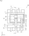
- FIG. 1 is a schematic top view of the semiconductor device 100 of the present embodiment.
- FIG. 2 is a schematic cross-sectional view of a main part of the semiconductor device 100 of the present embodiment.
- FIG. 2 is a schematic diagram of a cross section taken along line A-A' in FIG. 1 .
- FIG. 3A-B are schematic diagrams of a cross section taken along line A-A' in FIG. 1 .
- FIG. 3A is a schematic view of a A-A' cross-section in the vicinity of a second bonding material 20a.
- FIG. 3B is a schematic view of a A-A' cross-section in the vicinity of the second bonding material 20b.
- a sealing resin 82 is also shown. In FIG. 1 and FIG. 2 , the sealing resin 82 is not illustrated.
- the semiconductor device 100 of the present embodiment will be described using FIG. 1 , FIG. 2 and FIG. 3A-B .
- a lead frame 2 is a member on which a semiconductor chip 10 is disposed and includes a conductive material such as Cu (copper).
- the lead frame 2 includes a first bed 3 and a first outer lead 6.
- the first bed 3 includes a first bed surface 4.
- the semiconductor chip 10 is provided on the first bed surface 4.
- the first outer lead 6 is connected to the first bed 3.
- the first outer lead 6 is used to connect the semiconductor chip 10 and an external circuit (not shown).
- a first bonding material 70 is provided between the first bed surface 4 of the lead frame 2 and the semiconductor chip 10.
- the first bonding material 70 is provided on the first bed surface 4 of the lead frame 2.
- the first bonding material 70 joins a drain electrode (an example of a first electrode) 11 of the semiconductor chip 10 and the first bed surface 4.
- the semiconductor chip 10 is provided with a MOSFET, the first bonding material 70 connects the drain electrode 11 of the semiconductor chip 10 and the first bed surface 4.
- the semiconductor chip 10 is provided on the first bonding material 70.
- the semiconductor chip 10 has a lower surface 10a, and an upper surface 10b. Further, the semiconductor chip 10 includes the drain electrode 11 provided on the lower surface 10a, a source electrode (an example of a second electrode) 16 provided on the upper surface 10b, a plurality of electrode pads 17 provided on the source electrode 16, and a third insulating film 12 provided on the source electrode 16.
- the semiconductor chip 10 is, for example, a chip in which the vertical MOSFET or an IGBT(Insulated Gate Bipolar Transistor) or the like is provided on a semiconductor substrate such as an Si (silicon) substrate, an SiC (silicon carbide) substrate, a GaAs (gallium arsenide) substrate, or a GaN (gallium nitride) substrate.
- a semiconductor substrate such as an Si (silicon) substrate, an SiC (silicon carbide) substrate, a GaAs (gallium arsenide) substrate, or a GaN (gallium nitride) substrate.
- an X-direction, a Y-direction vertically intersecting with the X-direction, and a Z-direction vertically intersecting with the X-direction and the Y-direction are defined. It is assumed that the first bed surface 4, the lower surface 10a and the upper surface 10b are provided parallel to the XY plane.
- the source electrode 16 corresponds to a source electrode of such a MOSFET.
- the source electrode 16 includes, for example, Al (aluminum).
- the third insulating film 12 is provided on the source electrode 16 of the semiconductor chip 10.
- the third insulating film 12 is provided, for example, on an end of the semiconductor chip 10 and on an end of the source electrode 16.
- the third insulating film 12 has an opening 13a and an opening 13b on the source electrode 16.
- the opening 13a and the opening 13b pass through the third insulating film 12.
- the third insulating film 12 includes, for example, an insulating material such as polyimide. Note that the number of the openings 13 is not limited to those shown in this embodiment.
- the plurality of electrode pads 17 are provided in the opening 13 on the source electrode 16.
- the plurality of electrode pads 17 are connected to the source electrode 16.
- An electrode pad 17a is provided on the source electrode 16 in the opening 13a.
- An electrode pad 17b is provided on the source electrode 16 in the opening 13b. Note that the number of electrode pads 17 is not limited to those shown in this embodiment.
- the electrode pad 17 includes, for example, a first layer 14 including Ni (nickel) and a second layer 15 provided on the first layer 14 and including Au (gold).
- the configuration of the electrode pad 17 is not limited to that described above.
- the electrode pad 17 may include an alloy of Ni and Au.
- the electrode pad 17 may include a layer containing Ni, a layer containing Pd (palladium) provided on the layer containing Ni, and a layer containing Au provided on the layer containing Pd. Further, the electrode pad 17 may contain Cu, for example. Further, the electrode pad 17 may have, for example, layers including Cu. The electrode pad 17 is provided, for example, to increase the bonding strength between the source electrode 16 and the second bonding material 20.
- a plurality of second bonding materials 20 are provided on each of the electrode pads 17.
- a second bonding material 20a is provided on the electrode pad 17a.
- a second bonding material 20b is provided on the electrode pad 17b.
- the second bonding material 20 may be referred to as a metal layer.
- a first connector 50 includes a first end 51a and a second end 51b.
- the first connector 50 includes, for example, a conductive material such as Cu.
- the surface of the first connector 50 may be plated by a material containing, for example, Tin (Sn).
- the first end 51a is provided on the second bonding material 20a in the opening 13 and is connected to the second bonding material 20a.
- the first connector 50 is electrically connected to the electrode pad 17a via the second bonding material 20a.
- the first connector 50 is not connected to the second bonding material 20b.
- the first connector 50 is not connected to the electrode pad 17b via the second bonding material 20b.
- the second end 51b is provided on the second bed 58 and is connected to the second bed 58 using a third bonding material 59.
- the first connector 50 is provided to extend in the Y-direction and straddles between the first post 54 and the lead frame 2. Incidentally, even when the electrode pad 17a and the second bed 58 are connected using a wire instead of the first connector 50, such wire is not connected to the second bonding material 20b. Further, such wire is not connected to the electrode pad 17a via the second bonding material 20b.
- the sealing resin 82 is provided on the third insulating film 12 and the second bonding material 20 so as to cover at least the third insulating film 12, the electrode pad 17, and the second bonding material 20.
- the sealing resin 82 is provided so as to cover around the second bonding material 20a and around the first end 51a of the first connector 50.
- the sealing resin 82 is provided so as to cover the second bonding material 20b. In this instance, the entire upper surface of the second bonding material 20b is in direct contact with the sealing resin 82.
- the sealing resin 82 includes, for example, a resin such as an epoxy resin. Further, the sealing resin 82 may include a filler such as silica or alumina.
- the first post 54 includes a second bed 58 and a second outer lead 56.
- the first post 54 includes a conductive material such as Cu.
- the second outer lead 56 is used for connecting the semiconductor chip 10 and an external circuit (not shown).
- a second post 64 includes a second bed 68 and a third outer lead 66.
- the second post 64 includes a conductive material such as Cu.
- the third outer lead 66 is used for connecting the semiconductor chip 10 and an external circuit (not shown).
- a third bonding material 59 is provided between the second bed 58 and the second end 51b.
- the third bonding material 59 connects the second bed 58 and the second end 51.
- a third connector 60 has a third end 61a and a fourth end 61b.
- the third connector 60 includes, for example, a conductive material such as Cu.
- the surface of the third connector 60 may be plated by a material containing, for example, Sn.
- the third end 61a is electrically connected to the semiconductor chip 10 via a fourth bonding material 80 provided on the semiconductor chip 10.
- the fourth bonding material 80 for example, is electrically connected to the gate electrode of MOSFET.
- the first connector 50 and the third connector 60 can not be easily bent and are hard connectors, which are different from wires used for bonding.
- a fifth bonding material 69 is provided between the second bed 68 and the fourth end 61b.
- the fifth bonding material 69 connects the second bed 68 and the fourth end 61b.
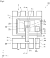
- FIG. 4 is a schematic top view of a semiconductor device 105 according to another aspect of the present embodiment.
- a wire 62 is used.
- the wire 62 may be used.
- An end 63a of the wire 62 is connected to the fourth bonding material 80.
- An end 63b of the wire 62 is connected to the fifth bonding material 69.
- first bonding material 70, the second bonding material 20, the third bonding material 59, the fourth bonding material 80, and the fifth bonding material 69 for example, solder containing Pb (lead) and Sn (tin), solder containing Pb, Ag (silver), and Sn (tin), solder containing Sn and Sb (antimony), solder containing Au (gold) and Sn, solder containing Au and Si, or solder containing Au and Ge (germanium), Ag paste, ultrasonic solder, or the like can be preferably used.
- FIG. 5 is a schematic top view of a semiconductor device 1000 as a first comparative embodiment of the present embodiment.
- the number of openings 13 and the number of second bonding material 20 are one.
- the number of electrode pads 17 (not shown) in FIG. 5 is also one.
- the area of the opening 13 in the XY-plane, the area of the second bonding material 20 in the XY-plane and the area of the electrode pad 17 in the XY-plane, respectively, are larger than those in the semiconductor device 100.
- the semiconductor chip 10 itself tends to warp due to internal stress of the semiconductor chip, for example, when the Z-direction is facing up.
- Ni is included in the electrode pad 17 due to the tensile stresses of Ni, so as to cancel the internal stress of the semiconductor chip, it was possible to suppress the warpage of the semiconductor chip and a wafer. In this way, carrying trouble of the semiconductor chip and the wafer is prevented.
- Cu is included in the electrode pad 17, similarly, it was possible to prevent the carrying trouble of the semiconductor chip and the wafer.
- the semiconductor device 1000 uses a connector 500 having a larger volume than the connector 50 used in the semiconductor device 100.
- the connector 500 includes an end 510a connected to the second bonding material 20 and an end 510b connected to the third bonding material 59.
- FIG. 6 is a schematic view of a cross section A-A' of the first comparative embodiment of the semiconductor device 1000 of the present embodiment. Arrows shown in the lead frame 2, the semiconductor chip 10, and the connector 500 schematically show a thermal expansion when the semiconductor device 1000 is heated by reliability assessment such as temperature cycling test.
- the thermal expansion coefficient of the semiconductor material such as Si used in semiconductor chip 10 is large. Therefore, due to the temperature rise of the semiconductor device 1000, the semiconductor chip 10 is stretched strongly in the XY plane. Therefore, by the reliability assessment such as thermal cycling test, the semiconductor chip 10 cracks, and it was sometimes impossible to achieve high reliability.
- FIG. 7 is a schematic top view of a semiconductor device 1100 as a second comparative embodiment of the present embodiment.
- the number of openings 13 and the number of second bonding materials 20 are one.
- the number of electrode pads 17 (not shown) in FIG. 7 is also one.
- the area of the opening 13 in the XY-plane, the area of the second bonding material 20 in the XY-plane, and the area of the electrode pad 17 in the XY-plane, respectively, are smaller than that of the semiconductor device 1100.
- the volume of the connector 50 is reduced to less than the volume of the connector 500 of the semiconductor device 1100 shown in FIG. 5 and FIG. 6 .
- the connector 50 having a small volume, the area of electrode pad 17 has become smaller. Therefore, the tensile stresses of the above electrode pad 17 is reduced, it was sometimes impossible to suppress warpage of the semiconductor chip and the wafer. Therefore, the semiconductor chip and the wafer may not be transported in some cases.
- the semiconductor device 100 of the present embodiment includes the first connector 50 which is electrically connected to at least one of the plurality of electrode pads 17.
- FIG. 8 is a schematic diagram showing the operation and effects of the semiconductor device 100 of the present embodiment. Arrows shown in the lead frame 2, the semiconductor chip 10 and the connector 50 schematically show thermal expansion due to temperature rise of the semiconductor device 100.
- the reduced volume of the first connector 50 reduces the thermal expansion of the first connector 50. Therefore, cracks in the semiconductor chip 10 are less likely to occur. Furthermore, by providing the second bonding material 20b which is not connected to the first connector 50 or the wire, warpage due to internal stress in the semiconductor chip or the wafer state can be canceled out by the tensile stresses of the electrode pad 17b provided below the second bonding material 20b. Therefore, it is possible to suppress warpage of semiconductor chip and the wafer state. This can prevent the carrying trouble of the semiconductor chip and the wafer. Therefore, it is possible to provide a semiconductor device 100 with improved reliability.
- the second bonding material 20b which is not electrically connected to the first connector 50 is covered with the sealing resin 82. Or, the second bonding material 20b which is not electrically connected to the first connector 50 is not connected to the connector or the wire.
- the semiconductor device 100 with improved reliability can be provided.
- the semiconductor device of the present embodiment is different from the semiconductor device of the first embodiment in that the semiconductor device of the present embodiment further includes a first semiconductor layer of first conductivity type provided on the first electrode, a first semiconductor region of second conductivity type provided on the first semiconductor layer, a second semiconductor region of first conductivity type provided on the first semiconductor region, the second electrode provided on the second semiconductor region, the second electrode being electrically connected to the second semiconductor region, and a third electrode provided in a first trench, the first trench reaching the first semiconductor layer from above the first semiconductor region, the third electrode facing the first semiconductor layer via a first insulating film, wherein the first trench extends in a first direction parallel to the upper surface, and wherein the electrode pad which is provided above the first trench and which is not connected to the first connector via the second bonding material extends in a second direction, the second direction is parallel to the upper surface and intersects the first direction.
- the semiconductor device of the present embodiment is different from the semiconductor device of the first embodiment in that the semiconductor device of the present embodiment further includes a first semiconductor layer (112) of first conductivity type provided on the first electrode (11), a first semiconductor region (114) of second conductivity type provided on the first semiconductor layer (112), a second semiconductor region (116) of first conductivity type provided on the first semiconductor region (114), and a third electrode (128) provided in a first trench (119), the first trench (119) reaching the first semiconductor layer (112) from above the first semiconductor region (114), the thi129second rd electrode (128) facing the first semiconductor layer (112) via a first insulating film (112), wherein the second electrode (16) is provided on the second semiconductor region (116) and is electrically connected to the second semiconductor region (116), wherein the first trench (119) extends in a first direction (Y-direction) parallel to the upper surface (10b), and wherein the third electrode pad (17b) is provided above the first trench (119) and extends in a second direction (X-direction)
- FIG. 9 is a schematic top view of a semiconductor device 110 of the present embodiment.
- FIG. 9 the second bonding material 20 is not shown, and the electrode pad 17 provided below the second bonding material 20 is shown. The same shall apply to FIG. 10 and subsequent figures.
- the first end 51a of the first connector 50 is connected to the electrode pad 17a 1 and the electrode pad 17a 2 via the second bonding material 20. Further, the second bonding material 20a 1 and the second bonding material 20a 2 are provided on the electrode pad 17a 1 and the electrode pad 17a 2 . The first end 51a may be connected to one electrode pad.
- each electrode pad 17b extends in the X-direction.
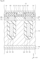
- FIG. 10 is a schematic cross-sectional view of a main part of a semiconductor device 110 of the present embodiment.
- Trench-type MOSFET is provided in the semiconductor chip 10 of semiconductor device 110.
- trench-type IGBT may be provided in the semiconductor chip 10.
- the drain electrode 11 functions as MOSFET's drain electrode.
- a drain layer 109 is provided on the drain electrode 11.
- the drain layer 109 includes, for example, a n + type semiconductor material.
- a drift layer (an example of a first semiconductor layer) 112 is provided on the drain layer 109.
- the drift layer 112 functions as a drift layer of the MOSFET.
- the drift layer 112 includes, for example, an n - type semiconductor material.
- a base region (an example of a first semiconductor region) 114 is provided on the drift layer 112.
- the base region 114 functions as a base of the MOSFET.
- the base region 114 is a region that forms a channel when a voltage is applied to the gate electrode 128 to be described later, allowing carriers to flow between the drain layer 109 and source region 116 to be described later.
- the base region 114 contains, for example, a p-type semiconductor material.
- a source region (an example of a second semiconductor region) 116 is provided on the base region 114.
- the source region 116 functions as a source of the MOSFET. Carriers flow between the source region 116 and the drain layer 109 when appropriate voltage is applied to the gate electrode 128, which will be described later.
- the source region 116 includes, for example, a n + type semiconductor material.
- the contact region 118 is provided on the base region 114 and is electrically connected to the base region 114 and the source region 116.
- the contact region 118 is provided in order to improve electrical contact of the base region 114 and the source region 116 with the source electrode 16.
- the contact region 118 includes, for example, a p + type semiconductor material.
- a trench 119 is provided to reach the drift layer 112 from above the base region 114 and the source region 116.
- the trench 119 extends in the back direction of the figure (Y-direction, which is an example of a first direction). In other words, the trench 119 extends in the Y direction perpendicular to the direction in which electrode pad 17b extends (X-direction, an example of a second direction).
- a first insulating film 122 is provided in the trench 119.
- the first insulating film 122 is provided so as to cover a field plate electrode 124, which will be described later.
- the first insulating film 122 is a field plate insulating film.
- the first insulating film 122 is provided between the field plate electrode 124 and the gate electrode 128.
- the form of the first insulating film 122 is not limited to this form.
- the first insulating film 122 includes, but is not limited to, SiO x (silicon oxide).
- a fifth insulating film 121 is provided, in the trench 119, between the base region 114 and the gate electrode 128 on the first insulating film 122 and between the interlayer insulating film 195 which will be described later and the source region 116 on the first insulating film 122.
- the fifth insulating film 121 is a gate insulating film.
- the fifth insulating film 121 includes, but is not limited to, SiO x (silicon oxide).
- the field plate electrode (an example of a third electrode) 124 is provided in the trench 119 so as to face the drift layer 112 via the first insulating film 122.
- the field plate electrode 124 is provided side by side with the drift layer 112.
- the field plate electrode 124 extends in the Y-direction.
- the field plate electrode 124 for example, is provided to assist extending the depletion layer from the base region 114 to the drift layer 112, and to increase the breakdown voltage.
- the gate electrode 128 is provided above the field plate electrode 124.
- the gate electrode 128 is provided between the plurality of base regions 114 via the fifth insulating films 121.
- the gate electrode 128 extends in the Y-direction.
- the gate electrode 128 is an electrode that serves as a gate for MOSFET.
- the interlayer insulating film 195 is provided above the source region 116, on the gate electrode 128, and on the fifth insulating film 121.
- the interlayer insulating film 195 includes, for example, but is not limited to, SiO x .
- the source electrode 16 is provided on the source region 116 and the contact region 118, and is electrically connected to the source region 116 and the contact region 118.
- the electrode pads 17 are appropriately provided on the source electrode 16.
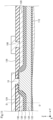
- FIG. 11 is a schematic cross-sectional view of a main part of semiconductor device 110 of the present embodiment.
- FIG. 11 is a schematic cross-sectional view for showing an example of a connection method of the field plate electrode 124 and the source electrode 16 and an example of a connection method of the gate electrode 128 and the gate metal 198.
- a schematic cross-sectional view of FIG. 10 corresponds to a schematic cross-sectional view in a D-D' cross-section of FIG. 11 .
- the field plate electrode 124 has a portion extending in the Z-direction.
- the field plate electrode 124 is electrically connected to the source electrode 16 through a contact hole formed in the interlayer insulating film 195 by using the portion extending in the Z-direction.
- the gate electrode 128 is electrically connected to the gate metal 198 through a contact hole provided in the interlayer insulating film 195.
- the gate metal 198 is provided below the fourth bonding material 80 ( FIG. 1 ) and is electrically connected to the fourth bonding material 80.
- the portion 129 of gate electrode 128 extending in the Y-direction may be provided, for example, below between the electrode pad 17a 1 and the electrode pad 17a 2 ( FIG. 9 ).
- the portion 129 of the gate electrode 128 extending in the Y-direction is an example of a conductive line, or a connection wiring connected to the gate electrode 128.
- the plurality of second bonding materials (20) includes the plurality of third bonding materials (20a) joined to the first connector (50), and the semiconductor device further includes a connection wiring (129) connected to the third electrode (128) and provided below between the third bonding materials (20a).
- the semiconductor chip 10 having the trench 19 has a higher internal stress and tends to warp in a plane perpendicular to the direction in which trench 119 extends.
- the internal stress is higher in the XZ-plane than in the YZ-plane, and the semiconductor chip 10 tends to warp .
- electrode pad 17 is provided so as to extend in the X-direction.
- the warpage of the semiconductor chip 10 in the XZ plane can be suppressed better.
- the semiconductor device 110 of the present embodiment can also provide the semiconductor device with improved reliability.
- the semiconductor device of the present embodiment is different from the semiconductor device of the first and second embodiments in that the semiconductor device of the present embodiment further includes a fourth electrode provided in a second trench, the second trench reaching the first semiconductor layer from above the first semiconductor region, the fourth electrode facing the first semiconductor layer via a second insulating film, wherein the second trench extends in a third direction parallel to the upper surface and intersecting the first direction, and wherein the electrode pad which is provided above the second trench and which is not connected to the first connector via the second bonding material extends in a fourth direction, the fourth direction is parallel to the upper surface and intersects the third direction.
- the semiconductor device of the present embodiment is different from the semiconductor device of the first and second embodiments in that the semiconductor device of the present embodiment further includes a fourth electrode (128) provided in a second trench (119), the second trench (119) reaching the first semiconductor layer (112) from above the first semiconductor region (114), the fourth electrode (128) facing the first semiconductor layer (112) via a second insulating film (122), wherein the second trench (119) extends in a third direction (X-direction) parallel to the upper surface (10b) and intersecting the first direction (Y-direction), and wherein the first electrode pad (17c) provided above the second trench (129) and not electrically connected to the first connector (50) via the second bonding material (20) extend in a fourth direction (Y-direction), the fourth direction (Y-direction) is parallel to the upper surface (10b) and intersects the third direction (X-direction).
- description of contents overlapping with the first and second embodiments is omitted.
- FIG. 12 is a schematic top view of a semiconductor device 120 of the present embodiment.
- the electrode pads 17b extend in the X-direction (an example of a second direction).
- the trench 119 (an example of a first trench) below the electrode pads 17b, the first insulating film 122 (an example of a second insulating film) below the electrode pads 17b, and the field plate electrode 124 below the electrode pads 17b extend in the Y-direction (an example of a first direction).
- the electrode pads 17c extend in the Y-direction (an example of a fourth direction) .
- the trench 119 (an example of a second trench) below the electrode pads 17c, the first insulating film 122 (an example of a second insulating film) below the electrode pads 17c, and the field plate electrode 124 (an example of the fourth electrode) below the electrode pads 17c extend in the X-direction (an example of a third direction).
- the semiconductor device 120 of the present embodiment can also provide the semiconductor device with improved reliability.
- the semiconductor device of the present embodiment is different from the semiconductor device of the first embodiment in that a plurality of electrode pads which are not connected to the first connector is provided.
- descriptions of the same contents as those of the first to third embodiments are omitted.
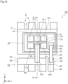
- FIG. 13 is a schematic top view of a semiconductor device 130 of the present embodiment.
- the electrode pad 17a is electrically connected to the first end 51a of the first connector 50.
- an electrode pad 17b, an electrode pad 17c, an electrode pad 17d, an electrode pad 17e and an electrode pad 17f are not electrically connected to the first connector 50.
- the semiconductor device 130 of the present embodiment can also provide the semiconductor device with improved reliability.
- the semiconductor device of the present embodiment is different from the semiconductor device of the fourth embodiment in that it includes a second connector connected to a plurality of electrode pads, and the electrode pads are not connected to the first connector.
- a second connector connected to a plurality of electrode pads, and the electrode pads are not connected to the first connector.
- FIG. 14 is a schematic top view of a semiconductor device 140 of the present embodiment.
- the second connector 53 is connected to the electrode pad 17b, the electrode pad 17c, the electrode pad 17d, the electrode pad 17e and the electrode pad 17f via the second bonding materials 20b, 20c, 20d, 20e and 20f (not illustrated).
- the semiconductor device 140 of the present embodiment includes a second connector (53) connected to the fourth bonding material (20) which is not connected to the first connector (50).
- the position of the first connector 50 may be shifted from the predetermined position and cured.
- the second connector 53 such a shift is suppressed.
- the semiconductor device 140 of the present embodiment can also provide the semiconductor device with improved reliability.
- FIG. 15 is a schematic top view of a semiconductor device 150 of the present embodiment. Descriptions overlapping with those of the first to fifth embodiments are omitted.
- the first connector 50 is connected to the electrode pad 17a and the electrode pad 17b. A connector and a wire are not connected to the electrode pad 17c and the electrode pad 17d.
- the semiconductor device 150 of the present embodiment can also provide the semiconductor device with improved reliability.
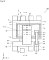
- FIG. 16 is a schematic top view of a semiconductor device 160 of the present embodiment. The description of the contents overlapping with the first embodiment to the sixth embodiment is omitted. The difference from the semiconductor device 150 shown in FIG. 15 is that the second connector 53 is connected to the electrode pad 17c and the electrode pad 17d.
- the semiconductor device 160 of the present embodiment can also provide the semiconductor device with improved reliability.
Landscapes
- Internal Circuitry In Semiconductor Integrated Circuit Devices (AREA)
- Wire Bonding (AREA)
Abstract
Description
- This application is based upon and claims the benefit of priority from
Japanese Patent Application No.2022-044781, filed on March 21, 2022 - Embodiments described herein relate generally to semiconductor device.
- A semiconductor device having a semiconductor chip such as a metal oxide semiconductor field effect transistor (MOSFET) is used for applications such as power conversion. For example, when semiconductor device described above is a vertical MOSFET, a source electrode provided on an upper surface of a semiconductor chip is connected to a connector provided on MOSFET, for example.
-
-
FIG. 1 is a schematic top view of a semiconductor device of a first embodiment. -
FIG. 2 is a schematic cross-sectional view of a main part of the semiconductor device of the first embodiment. -
FIG. 3A-B are schematic diagrams of a cross section taken along a line A-A' inFIG. 1 . -
FIG. 4 is a schematic top view of a semiconductor device according to another aspect of the first embodiment. -
FIG. 5 is a schematic top view of a semiconductor device as a first comparative embodiment of the first embodiment. -
FIG. 6 is a schematic diagram of a cross section taken along a line A-A' inFig. 5 . -
FIG. 7 is a schematic top view of a semiconductor device as a second comparative embodiment of the first embodiment. -
FIG. 8 is a schematic diagram showing the operation and effects of the semiconductor device of the first embodiment. -
FIG. 9 is a schematic top view of a semiconductor device of the second embodiment. -
FIG. 10 is a schematic cross-sectional view of a main part of the semiconductor device of the second embodiment. -
FIG. 11 is a schematic cross-sectional view of a main part of the semiconductor device of the second embodiment. -
FIG. 12 is a schematic top view of a semiconductor device of the third embodiment. -
FIG. 13 is a schematic top view of a semiconductor device of the fourth embodiment. -
FIG. 14 is a schematic top view of a semiconductor device of the fifth embodiment. -
FIG. 15 is a schematic top view of a semiconductor device of the sixth embodiment. -
FIG. 16 is a schematic top view of a semiconductor device of the seventh embodiment. - Hereinafter, embodiments of the present disclosure will be described with reference to the drawings. Note that in the following description, the same members and the like are denoted by the same reference numerals, and description of members and the like once described is appropriately omitted.
- In this specification, in order to illustrate the positional relationship of parts and the like, the upward direction of the drawings may be referred to as "upper", and the downward direction of the drawings may be referred to as "lower". Here, the terms "up" and "down" do not necessarily indicate a relationship with the direction of gravity.
- Hereinafter, a case where a first conductivity type is n-type and a second conductivity type is p-type will be exemplified.
- In the following description, notations of n+, n, n-, p+, p, and p- indicate a relative level of an impurity concentration of each of the conductivity types. That is, n+ indicates that an impurity concentration of n-type is relatively higher than n, and n- indicates that the impurity concentration of n-type is relatively lower than n. p+ indicates that an impurity concentration of p-type is relatively higher than p, and p- indicates that the impurity concentration of p-type is relatively lower than p. Note that n+ type and n- type may be simply referred to as n type, and p+ type and p- type may be simply referred to as p type.
- The semiconductor device of the present embodiment includes a lead frame; a first bonding material provided on the lead frame; a semiconductor chip provided on the first bonding material, the semiconductor chip including a lower surface, an upper surface, a first electrode provided on the lower surface, the first electrode being connected to the first bonding material, a second electrode provided on the upper surface, and a plurality of electrode pads connected to the second electrode; a plurality of second bonding materials, each of the second bonding materials being provided on each of the electrode pads; and a first connector connected to at least one of the second bonding materials, wherein the second bonding material which is not connected to the first connector is not connected to a connector or a wire. The semiconductor device of the present embodiment includes a lead frame (2); a first bonding material (70) provided on the lead frame (2); a semiconductor chip (10) provided on the first bonding material (70), the semiconductor chip (10) including a lower surface (10a), an upper surface (10b), a first electrode (11) provided on the lower surface (10a), the first electrode (11) being connected to the first bonding material (70), a second electrode (16) provided on the upper surface (10b), and a plurality of first electrode pads (17) connected to the second electrode (16); a plurality of second bonding materials (20), each of the second bonding materials (20) being provided on each of the first electrode pads (17); and a first connector (50), wherein the second bonding materials (20) includes at least one third bonding material (20a) which is joined (bonded) to the first connector (50) and a fourth bonding material (20b) which is not connected to the first connector (50) or a wire (62), and wherein the first electrode pads (17) include at least one second electrode pad (17a) provided below the third bonding material (20a) and a third electrode pad (17b) provided below the fourth bonding material (20b).
- The semiconductor device of the present embodiment includes a lead frame; a first bonding material provided on the lead frame; a semiconductor chip provided on the first bonding material, the semiconductor chip including a lower surface, an upper surface, a first electrode provided on the lower surface, the first electrode being connected to the first bonding material, a second electrode provided on the upper surface, and a plurality of electrode pads connected to the second electrode; a plurality of second bonding materials, each of the second bonding materials being provided on each of the electrode pads; a first connector connected to at least one of the second bonding materials; and a sealing resin provided on the second bonding material not being connected to the first connector. The semiconductor device of the present embodiment includes a lead frame (2); a first bonding material (70) provided on the lead frame (2); a semiconductor chip (10) provided on the first bonding material (70), the semiconductor chip (10) including a lower surface (10a), an upper surface (10b), a first electrode (11) provided on the lower surface (10a), the first electrode (11) being connected to the first bonding material (70), a second electrode (16) provided on the upper surface (10b), and a plurality of first electrode pads (17) connected to the second electrode (16); a plurality of second bonding materials (20), each of the second bonding materials (20) being provided on each of the first electrode pads (17); a first connector (50) connected to at least one of the second bonding materials (20); and a sealing resin (82), wherein the second bonding materials (20) further include a fourth bonding material (20b) which is not connected to the first connector (50), and wherein the sealing resin (82) is provided on the fourth bonding material (82).
-
FIG. 1 is a schematic top view of thesemiconductor device 100 of the present embodiment.FIG. 2 is a schematic cross-sectional view of a main part of thesemiconductor device 100 of the present embodiment.FIG. 2 is a schematic diagram of a cross section taken along line A-A' inFIG. 1 .FIG. 3A-B are schematic diagrams of a cross section taken along line A-A' inFIG. 1 .FIG. 3A is a schematic view of a A-A' cross-section in the vicinity of asecond bonding material 20a.FIG. 3B is a schematic view of a A-A' cross-section in the vicinity of thesecond bonding material 20b. InFIG. 3A and FIG. 3B , asealing resin 82 is also shown. InFIG. 1 andFIG. 2 , thesealing resin 82 is not illustrated. - The
semiconductor device 100 of the present embodiment will be described usingFIG. 1 ,FIG. 2 andFIG. 3A-B . - A
lead frame 2 is a member on which asemiconductor chip 10 is disposed and includes a conductive material such as Cu (copper). Thelead frame 2 includes afirst bed 3 and a firstouter lead 6. Thefirst bed 3 includes afirst bed surface 4. Thesemiconductor chip 10 is provided on thefirst bed surface 4. The firstouter lead 6 is connected to thefirst bed 3. The firstouter lead 6 is used to connect thesemiconductor chip 10 and an external circuit (not shown). - A
first bonding material 70 is provided between thefirst bed surface 4 of thelead frame 2 and thesemiconductor chip 10. Thefirst bonding material 70 is provided on thefirst bed surface 4 of thelead frame 2. Thefirst bonding material 70 joins a drain electrode (an example of a first electrode) 11 of thesemiconductor chip 10 and thefirst bed surface 4. For example, if thesemiconductor chip 10 is provided with a MOSFET, thefirst bonding material 70 connects thedrain electrode 11 of thesemiconductor chip 10 and thefirst bed surface 4. - The
semiconductor chip 10 is provided on thefirst bonding material 70. Thesemiconductor chip 10 has a lower surface 10a, and anupper surface 10b. Further, thesemiconductor chip 10 includes thedrain electrode 11 provided on the lower surface 10a, a source electrode (an example of a second electrode) 16 provided on theupper surface 10b, a plurality ofelectrode pads 17 provided on thesource electrode 16, and a third insulatingfilm 12 provided on thesource electrode 16. Thesemiconductor chip 10 is, for example, a chip in which the vertical MOSFET or an IGBT(Insulated Gate Bipolar Transistor) or the like is provided on a semiconductor substrate such as an Si (silicon) substrate, an SiC (silicon carbide) substrate, a GaAs (gallium arsenide) substrate, or a GaN (gallium nitride) substrate. - Here, an X-direction, a Y-direction vertically intersecting with the X-direction, and a Z-direction vertically intersecting with the X-direction and the Y-direction are defined. It is assumed that the
first bed surface 4, the lower surface 10a and theupper surface 10b are provided parallel to the XY plane. - For example, if the
semiconductor chip 10 is provided with a MOSFET, thesource electrode 16 corresponds to a source electrode of such a MOSFET. Thesource electrode 16 includes, for example, Al (aluminum). - The third
insulating film 12 is provided on thesource electrode 16 of thesemiconductor chip 10. The thirdinsulating film 12 is provided, for example, on an end of thesemiconductor chip 10 and on an end of thesource electrode 16. The thirdinsulating film 12 has anopening 13a and anopening 13b on thesource electrode 16. Theopening 13a and theopening 13b pass through the third insulatingfilm 12. The thirdinsulating film 12 includes, for example, an insulating material such as polyimide. Note that the number of theopenings 13 is not limited to those shown in this embodiment. - The plurality of
electrode pads 17 are provided in theopening 13 on thesource electrode 16. The plurality ofelectrode pads 17 are connected to thesource electrode 16. Anelectrode pad 17a is provided on thesource electrode 16 in theopening 13a. Anelectrode pad 17b is provided on thesource electrode 16 in theopening 13b. Note that the number ofelectrode pads 17 is not limited to those shown in this embodiment. Theelectrode pad 17 includes, for example, afirst layer 14 including Ni (nickel) and asecond layer 15 provided on thefirst layer 14 and including Au (gold). The configuration of theelectrode pad 17 is not limited to that described above. For example, theelectrode pad 17 may include an alloy of Ni and Au. For example, theelectrode pad 17 may include a layer containing Ni, a layer containing Pd (palladium) provided on the layer containing Ni, and a layer containing Au provided on the layer containing Pd. Further, theelectrode pad 17 may contain Cu, for example. Further, theelectrode pad 17 may have, for example, layers including Cu. Theelectrode pad 17 is provided, for example, to increase the bonding strength between thesource electrode 16 and thesecond bonding material 20. - A plurality of
second bonding materials 20 are provided on each of theelectrode pads 17. Asecond bonding material 20a is provided on theelectrode pad 17a. Asecond bonding material 20b is provided on theelectrode pad 17b. Thesecond bonding material 20 may be referred to as a metal layer. - A
first connector 50 includes afirst end 51a and asecond end 51b. Thefirst connector 50 includes, for example, a conductive material such as Cu. Incidentally, the surface of thefirst connector 50 may be plated by a material containing, for example, Tin (Sn). Thefirst end 51a is provided on thesecond bonding material 20a in theopening 13 and is connected to thesecond bonding material 20a. Thus, thefirst connector 50 is electrically connected to theelectrode pad 17a via thesecond bonding material 20a. On the other hand, thefirst connector 50 is not connected to thesecond bonding material 20b. Thefirst connector 50 is not connected to theelectrode pad 17b via thesecond bonding material 20b. Thesecond end 51b is provided on thesecond bed 58 and is connected to thesecond bed 58 using athird bonding material 59. Thefirst connector 50 is provided to extend in the Y-direction and straddles between thefirst post 54 and thelead frame 2. Incidentally, even when theelectrode pad 17a and thesecond bed 58 are connected using a wire instead of thefirst connector 50, such wire is not connected to thesecond bonding material 20b. Further, such wire is not connected to theelectrode pad 17a via thesecond bonding material 20b. - The sealing
resin 82 is provided on the third insulatingfilm 12 and thesecond bonding material 20 so as to cover at least the third insulatingfilm 12, theelectrode pad 17, and thesecond bonding material 20. Here, as shown inFIG. 3A , around thesecond bonding material 20a, the sealingresin 82 is provided so as to cover around thesecond bonding material 20a and around thefirst end 51a of thefirst connector 50. On the other hand, as shown inFIG. 3B , around thesecond bonding material 20b, the sealingresin 82 is provided so as to cover thesecond bonding material 20b. In this instance, the entire upper surface of thesecond bonding material 20b is in direct contact with the sealingresin 82. The sealingresin 82 includes, for example, a resin such as an epoxy resin. Further, the sealingresin 82 may include a filler such as silica or alumina. - The
first post 54 includes asecond bed 58 and a secondouter lead 56. Thefirst post 54 includes a conductive material such as Cu. The secondouter lead 56 is used for connecting thesemiconductor chip 10 and an external circuit (not shown). - A
second post 64 includes asecond bed 68 and a thirdouter lead 66. Thesecond post 64 includes a conductive material such as Cu. The thirdouter lead 66 is used for connecting thesemiconductor chip 10 and an external circuit (not shown). - A
third bonding material 59 is provided between thesecond bed 58 and thesecond end 51b. Thethird bonding material 59 connects thesecond bed 58 and the second end 51. - A
third connector 60 has athird end 61a and afourth end 61b. Thethird connector 60 includes, for example, a conductive material such as Cu. Incidentally, the surface of thethird connector 60 may be plated by a material containing, for example, Sn. Thethird end 61a is electrically connected to thesemiconductor chip 10 via afourth bonding material 80 provided on thesemiconductor chip 10. Thefourth bonding material 80, for example, is electrically connected to the gate electrode of MOSFET. - Incidentally, the
first connector 50 and thethird connector 60 can not be easily bent and are hard connectors, which are different from wires used for bonding. - A
fifth bonding material 69 is provided between thesecond bed 68 and thefourth end 61b. Thefifth bonding material 69 connects thesecond bed 68 and thefourth end 61b. -
FIG. 4 is a schematic top view of asemiconductor device 105 according to another aspect of the present embodiment. Instead of thethird connector 60, awire 62 is used. Instead of thethird connector 60, thewire 62 may be used. Anend 63a of thewire 62 is connected to thefourth bonding material 80. Anend 63b of thewire 62 is connected to thefifth bonding material 69. - As the
first bonding material 70, thesecond bonding material 20, thethird bonding material 59, thefourth bonding material 80, and thefifth bonding material 69, for example, solder containing Pb (lead) and Sn (tin), solder containing Pb, Ag (silver), and Sn (tin), solder containing Sn and Sb (antimony), solder containing Au (gold) and Sn, solder containing Au and Si, or solder containing Au and Ge (germanium), Ag paste, ultrasonic solder, or the like can be preferably used. - Next, the operation and effects of semiconductor device of the present embodiment will be described.
-
FIG. 5 is a schematic top view of asemiconductor device 1000 as a first comparative embodiment of the present embodiment. The number ofopenings 13 and the number ofsecond bonding material 20 are one. Then, the number of electrode pads 17 (not shown) inFIG. 5 is also one. Further, the area of theopening 13 in the XY-plane, the area of thesecond bonding material 20 in the XY-plane and the area of theelectrode pad 17 in the XY-plane, respectively, are larger than those in thesemiconductor device 100. - The
semiconductor chip 10 itself tends to warp due to internal stress of the semiconductor chip, for example, when the Z-direction is facing up. On the other hand, particularly when Ni is included in theelectrode pad 17, due to the tensile stresses of Ni, so as to cancel the internal stress of the semiconductor chip, it was possible to suppress the warpage of the semiconductor chip and a wafer. In this way, carrying trouble of the semiconductor chip and the wafer is prevented. Incidentally, for example, even when Cu is included in theelectrode pad 17, similarly, it was possible to prevent the carrying trouble of the semiconductor chip and the wafer. - In order to reduce the on-resistance of the semiconductor device as much as possible, the
semiconductor device 1000 uses aconnector 500 having a larger volume than theconnector 50 used in thesemiconductor device 100. Theconnector 500 includes anend 510a connected to thesecond bonding material 20 and anend 510b connected to thethird bonding material 59. -
FIG. 6 is a schematic view of a cross section A-A' of the first comparative embodiment of thesemiconductor device 1000 of the present embodiment. Arrows shown in thelead frame 2, thesemiconductor chip 10, and theconnector 500 schematically show a thermal expansion when thesemiconductor device 1000 is heated by reliability assessment such as temperature cycling test. - Generally, as compared with the thermal expansion coefficient of the semiconductor material such as Si used in
semiconductor chip 10, the thermal expansion coefficient of Cu or the like used in thelead frame 2 and theconnector 500 is large. Therefore, due to the temperature rise of thesemiconductor device 1000, thesemiconductor chip 10 is stretched strongly in the XY plane. Therefore, by the reliability assessment such as thermal cycling test, thesemiconductor chip 10 cracks, and it was sometimes impossible to achieve high reliability. -
FIG. 7 is a schematic top view of asemiconductor device 1100 as a second comparative embodiment of the present embodiment. The number ofopenings 13 and the number ofsecond bonding materials 20 are one. Then, the number of electrode pads 17 (not shown) inFIG. 7 is also one. Further, the area of theopening 13 in the XY-plane, the area of thesecond bonding material 20 in the XY-plane, and the area of theelectrode pad 17 in the XY-plane, respectively, are smaller than that of thesemiconductor device 1100. - To achieve high reliability, the volume of the
connector 50 is reduced to less than the volume of theconnector 500 of thesemiconductor device 1100 shown inFIG. 5 andFIG. 6 . Thus, at the time of temperature rise of thesemiconductor chip 10, it is suppressed that thesemiconductor chip 10 is stretched strongly in the XY-plane. However, in such cases, with the use of theconnector 50 having a small volume, the area ofelectrode pad 17 has become smaller. Therefore, the tensile stresses of theabove electrode pad 17 is reduced, it was sometimes impossible to suppress warpage of the semiconductor chip and the wafer. Therefore, the semiconductor chip and the wafer may not be transported in some cases. - Therefore, the
semiconductor device 100 of the present embodiment includes thefirst connector 50 which is electrically connected to at least one of the plurality ofelectrode pads 17. -
FIG. 8 is a schematic diagram showing the operation and effects of thesemiconductor device 100 of the present embodiment. Arrows shown in thelead frame 2, thesemiconductor chip 10 and theconnector 50 schematically show thermal expansion due to temperature rise of thesemiconductor device 100. - The reduced volume of the
first connector 50 reduces the thermal expansion of thefirst connector 50. Therefore, cracks in thesemiconductor chip 10 are less likely to occur. Furthermore, by providing thesecond bonding material 20b which is not connected to thefirst connector 50 or the wire, warpage due to internal stress in the semiconductor chip or the wafer state can be canceled out by the tensile stresses of theelectrode pad 17b provided below thesecond bonding material 20b. Therefore, it is possible to suppress warpage of semiconductor chip and the wafer state. This can prevent the carrying trouble of the semiconductor chip and the wafer. Therefore, it is possible to provide asemiconductor device 100 with improved reliability. - The
second bonding material 20b which is not electrically connected to thefirst connector 50 is covered with the sealingresin 82. Or, thesecond bonding material 20b which is not electrically connected to thefirst connector 50 is not connected to the connector or the wire. - According to the
semiconductor device 100 of the present embodiment, thesemiconductor device 100 with improved reliability can be provided. - The semiconductor device of the present embodiment is different from the semiconductor device of the first embodiment in that the semiconductor device of the present embodiment further includes a first semiconductor layer of first conductivity type provided on the first electrode, a first semiconductor region of second conductivity type provided on the first semiconductor layer, a second semiconductor region of first conductivity type provided on the first semiconductor region, the second electrode provided on the second semiconductor region, the second electrode being electrically connected to the second semiconductor region, and a third electrode provided in a first trench, the first trench reaching the first semiconductor layer from above the first semiconductor region, the third electrode facing the first semiconductor layer via a first insulating film, wherein the first trench extends in a first direction parallel to the upper surface, and wherein the electrode pad which is provided above the first trench and which is not connected to the first connector via the second bonding material extends in a second direction, the second direction is parallel to the upper surface and intersects the first direction. The semiconductor device of the present embodiment is different from the semiconductor device of the first embodiment in that the semiconductor device of the present embodiment further includes a first semiconductor layer (112) of first conductivity type provided on the first electrode (11), a first semiconductor region (114) of second conductivity type provided on the first semiconductor layer (112), a second semiconductor region (116) of first conductivity type provided on the first semiconductor region (114), and a third electrode (128) provided in a first trench (119), the first trench (119) reaching the first semiconductor layer (112) from above the first semiconductor region (114), the thi129second rd electrode (128) facing the first semiconductor layer (112) via a first insulating film (112), wherein the second electrode (16) is provided on the second semiconductor region (116) and is electrically connected to the second semiconductor region (116), wherein the first trench (119) extends in a first direction (Y-direction) parallel to the upper surface (10b), and wherein the third electrode pad (17b) is provided above the first trench (119) and extends in a second direction (X-direction) parallel to upper surface (10b) and intersecting the first direction (Y-direction). Here, description of the same content as that of semiconductor device of the first embodiment is omitted.
-
FIG. 9 is a schematic top view of asemiconductor device 110 of the present embodiment. - In
FIG. 9 , thesecond bonding material 20 is not shown, and theelectrode pad 17 provided below thesecond bonding material 20 is shown. The same shall apply toFIG. 10 and subsequent figures. - The
first end 51a of thefirst connector 50 is connected to theelectrode pad 17a1 and theelectrode pad 17a2 via thesecond bonding material 20. Further, thesecond bonding material 20a1 and thesecond bonding material 20a2 are provided on theelectrode pad 17a1 and theelectrode pad 17a2. Thefirst end 51a may be connected to one electrode pad. - Further, in the
semiconductor device 110, a plurality ofelectrode pads 17b is provided. Eachelectrode pad 17b extends in the X-direction. -
FIG. 10 is a schematic cross-sectional view of a main part of asemiconductor device 110 of the present embodiment. Trench-type MOSFET is provided in thesemiconductor chip 10 ofsemiconductor device 110. Incidentally, in thesemiconductor chip 10, for example, trench-type IGBT may be provided. - The
drain electrode 11 functions as MOSFET's drain electrode. - A
drain layer 109 is provided on thedrain electrode 11. Thedrain layer 109 includes, for example, a n+ type semiconductor material. - A drift layer (an example of a first semiconductor layer) 112 is provided on the
drain layer 109. Thedrift layer 112 functions as a drift layer of the MOSFET. Thedrift layer 112 includes, for example, an n- type semiconductor material. - A base region (an example of a first semiconductor region) 114 is provided on the
drift layer 112. Thebase region 114 functions as a base of the MOSFET. Thebase region 114 is a region that forms a channel when a voltage is applied to thegate electrode 128 to be described later, allowing carriers to flow between thedrain layer 109 andsource region 116 to be described later. Thebase region 114 contains, for example, a p-type semiconductor material. - A source region (an example of a second semiconductor region) 116 is provided on the
base region 114. Thesource region 116 functions as a source of the MOSFET. Carriers flow between thesource region 116 and thedrain layer 109 when appropriate voltage is applied to thegate electrode 128, which will be described later. Thesource region 116 includes, for example, a n+ type semiconductor material. - The
contact region 118 is provided on thebase region 114 and is electrically connected to thebase region 114 and thesource region 116. Thecontact region 118 is provided in order to improve electrical contact of thebase region 114 and thesource region 116 with thesource electrode 16. Thecontact region 118 includes, for example, a p+ type semiconductor material. - A
trench 119 is provided to reach thedrift layer 112 from above thebase region 114 and thesource region 116. Thetrench 119 extends in the back direction of the figure (Y-direction, which is an example of a first direction). In other words, thetrench 119 extends in the Y direction perpendicular to the direction in whichelectrode pad 17b extends (X-direction, an example of a second direction). - A first insulating
film 122 is provided in thetrench 119. For example, the first insulatingfilm 122 is provided so as to cover afield plate electrode 124, which will be described later. The firstinsulating film 122 is a field plate insulating film. For example, the first insulatingfilm 122 is provided between thefield plate electrode 124 and thegate electrode 128. However, the form of the first insulatingfilm 122 is not limited to this form. The firstinsulating film 122 includes, but is not limited to, SiOx (silicon oxide). - A fifth insulating
film 121 is provided, in thetrench 119, between thebase region 114 and thegate electrode 128 on the first insulatingfilm 122 and between the interlayer insulatingfilm 195 which will be described later and thesource region 116 on the first insulatingfilm 122. The fifthinsulating film 121 is a gate insulating film. The fifthinsulating film 121 includes, but is not limited to, SiOx (silicon oxide). - The field plate electrode (an example of a third electrode) 124 is provided in the
trench 119 so as to face thedrift layer 112 via the first insulatingfilm 122. For example, thefield plate electrode 124 is provided side by side with thedrift layer 112. Like thetrench 119, thefield plate electrode 124 extends in the Y-direction. Thefield plate electrode 124, for example, is provided to assist extending the depletion layer from thebase region 114 to thedrift layer 112, and to increase the breakdown voltage. - The
gate electrode 128 is provided above thefield plate electrode 124. Thegate electrode 128 is provided between the plurality ofbase regions 114 via the fifth insulatingfilms 121. Thegate electrode 128 extends in the Y-direction. Thegate electrode 128 is an electrode that serves as a gate for MOSFET. - The
interlayer insulating film 195 is provided above thesource region 116, on thegate electrode 128, and on the fifth insulatingfilm 121. Theinterlayer insulating film 195 includes, for example, but is not limited to, SiOx. - The
source electrode 16 is provided on thesource region 116 and thecontact region 118, and is electrically connected to thesource region 116 and thecontact region 118. The electrode pads 17 (not shown inFIG. 10 ) are appropriately provided on thesource electrode 16. -
FIG. 11 is a schematic cross-sectional view of a main part ofsemiconductor device 110 of the present embodiment.FIG. 11 is a schematic cross-sectional view for showing an example of a connection method of thefield plate electrode 124 and thesource electrode 16 and an example of a connection method of thegate electrode 128 and thegate metal 198. For example, a schematic cross-sectional view ofFIG. 10 corresponds to a schematic cross-sectional view in a D-D' cross-section ofFIG. 11 . - The
field plate electrode 124 has a portion extending in the Z-direction. Thefield plate electrode 124 is electrically connected to thesource electrode 16 through a contact hole formed in theinterlayer insulating film 195 by using the portion extending in the Z-direction. - The
gate electrode 128 is electrically connected to thegate metal 198 through a contact hole provided in theinterlayer insulating film 195. For example, thegate metal 198 is provided below the fourth bonding material 80 (FIG. 1 ) and is electrically connected to thefourth bonding material 80. - Note that the
portion 129 ofgate electrode 128 extending in the Y-direction may be provided, for example, below between theelectrode pad 17a1 and theelectrode pad 17a2 (FIG. 9 ). In such cases, theportion 129 of thegate electrode 128 extending in the Y-direction is an example of a conductive line, or a connection wiring connected to thegate electrode 128. The plurality of second bonding materials (20) includes the plurality of third bonding materials (20a) joined to the first connector (50), and the semiconductor device further includes a connection wiring (129) connected to the third electrode (128) and provided below between the third bonding materials (20a). - Next, the operation and effects of semiconductor device of the present embodiment will be described.
- The
semiconductor chip 10 having the trench 19 has a higher internal stress and tends to warp in a plane perpendicular to the direction in whichtrench 119 extends. For example, as insemiconductor device 110, when thetrench 119 is extended in the Y-direction, the internal stress is higher in the XZ-plane than in the YZ-plane, and thesemiconductor chip 10 tends to warp . - Therefore, in the
semiconductor device 110,electrode pad 17 is provided so as to extend in the X-direction. Thus, the warpage of thesemiconductor chip 10 in the XZ plane can be suppressed better. - The
semiconductor device 110 of the present embodiment can also provide the semiconductor device with improved reliability. - The semiconductor device of the present embodiment is different from the semiconductor device of the first and second embodiments in that the semiconductor device of the present embodiment further includes a fourth electrode provided in a second trench, the second trench reaching the first semiconductor layer from above the first semiconductor region, the fourth electrode facing the first semiconductor layer via a second insulating film, wherein the second trench extends in a third direction parallel to the upper surface and intersecting the first direction, and wherein the electrode pad which is provided above the second trench and which is not connected to the first connector via the second bonding material extends in a fourth direction, the fourth direction is parallel to the upper surface and intersects the third direction. The semiconductor device of the present embodiment is different from the semiconductor device of the first and second embodiments in that the semiconductor device of the present embodiment further includes a fourth electrode (128) provided in a second trench (119), the second trench (119) reaching the first semiconductor layer (112) from above the first semiconductor region (114), the fourth electrode (128) facing the first semiconductor layer (112) via a second insulating film (122), wherein the second trench (119) extends in a third direction (X-direction) parallel to the upper surface (10b) and intersecting the first direction (Y-direction), and wherein the first electrode pad (17c) provided above the second trench (129) and not electrically connected to the first connector (50) via the second bonding material (20) extend in a fourth direction (Y-direction), the fourth direction (Y-direction) is parallel to the upper surface (10b) and intersects the third direction (X-direction). Here, description of contents overlapping with the first and second embodiments is omitted.
-
FIG. 12 is a schematic top view of asemiconductor device 120 of the present embodiment. - In a
first region 16a on thesource electrode 16, theelectrode pads 17b extend in the X-direction (an example of a second direction). The trench 119 (an example of a first trench) below theelectrode pads 17b, the first insulating film 122 (an example of a second insulating film) below theelectrode pads 17b, and thefield plate electrode 124 below theelectrode pads 17b extend in the Y-direction (an example of a first direction). - In a
second region 16b on thesource electrode 16, theelectrode pads 17c extend in the Y-direction (an example of a fourth direction) . The trench 119 (an example of a second trench) below theelectrode pads 17c, the first insulating film 122 (an example of a second insulating film) below theelectrode pads 17c, and the field plate electrode 124 (an example of the fourth electrode) below theelectrode pads 17c extend in the X-direction (an example of a third direction). - Even when the direction in which
trench 119 extends differs depending on the region, such as insemiconductor device 120, the warpage ofsemiconductor chip 10 can be suppressed better. - The
semiconductor device 120 of the present embodiment can also provide the semiconductor device with improved reliability. - The semiconductor device of the present embodiment is different from the semiconductor device of the first embodiment in that a plurality of electrode pads which are not connected to the first connector is provided. Here, descriptions of the same contents as those of the first to third embodiments are omitted.
-
FIG. 13 is a schematic top view of asemiconductor device 130 of the present embodiment. Theelectrode pad 17a is electrically connected to thefirst end 51a of thefirst connector 50. On the other hand, anelectrode pad 17b, anelectrode pad 17c, anelectrode pad 17d, anelectrode pad 17e and anelectrode pad 17f are not electrically connected to thefirst connector 50. - The
semiconductor device 130 of the present embodiment can also provide the semiconductor device with improved reliability. - The semiconductor device of the present embodiment is different from the semiconductor device of the fourth embodiment in that it includes a second connector connected to a plurality of electrode pads, and the electrode pads are not connected to the first connector. Here, descriptions of the same contents as those of the first to fourth embodiments are omitted.
-
FIG. 14 is a schematic top view of asemiconductor device 140 of the present embodiment. Thesecond connector 53 is connected to theelectrode pad 17b, theelectrode pad 17c, theelectrode pad 17d, theelectrode pad 17e and theelectrode pad 17f via thesecond bonding materials 20b, 20c, 20d, 20e and 20f (not illustrated). Thesemiconductor device 140 of the present embodiment includes a second connector (53) connected to the fourth bonding material (20) which is not connected to the first connector (50). - For example, when the
first connector 50 is connected to theelectrode pad 17a by reflow, when the melted bonding material is cured, the position of thefirst connector 50 may be shifted from the predetermined position and cured. By providing thesecond connector 53, such a shift is suppressed. - The
semiconductor device 140 of the present embodiment can also provide the semiconductor device with improved reliability. -
FIG. 15 is a schematic top view of asemiconductor device 150 of the present embodiment. Descriptions overlapping with those of the first to fifth embodiments are omitted. Thefirst connector 50 is connected to theelectrode pad 17a and theelectrode pad 17b. A connector and a wire are not connected to theelectrode pad 17c and theelectrode pad 17d. - The
semiconductor device 150 of the present embodiment can also provide the semiconductor device with improved reliability. -
FIG. 16 is a schematic top view of asemiconductor device 160 of the present embodiment. The description of the contents overlapping with the first embodiment to the sixth embodiment is omitted. The difference from thesemiconductor device 150 shown inFIG. 15 is that thesecond connector 53 is connected to theelectrode pad 17c and theelectrode pad 17d. - The
semiconductor device 160 of the present embodiment can also provide the semiconductor device with improved reliability. - While certain embodiments have been described, these embodiments have been presented by way of example only, and are not intended to limit the scope of the inventions. Indeed, the semiconductor device described herein may be embodied in a variety of other forms; furthermore, various omissions, substitutions and changes in the form of the devices and methods described herein may be made without departing from the spirit of the inventions. The accompanying claims and their equivalents are intended to cover such forms or modifications as would fall within the scope and spirit of the inventions.
- It is explicitly stated that all features disclosed in the description and/or the claims are intended to be disclosed separately and independently from each other for the purpose of original disclosure as well as for the purpose of restricting the claimed invention independent of the composition of the features in the embodiments and/or the claims. It is explicitly stated that all value ranges or indications of groups of entities disclose every possible intermediate value or intermediate entity for the purpose of original disclosure as well as for the purpose of restricting the claimed invention, in particular as limits of value ranges.
Claims (7)
- A semiconductor device (100) comprising:a lead frame (2);a first bonding material (70) provided on the lead frame (2);a semiconductor chip (10) provided on the first bonding material (70), the semiconductor chip (10) includinga lower surface (10a),an upper surface (10b),a first electrode (11) provided on the lower surface (10a), the first electrode (11) being connected to the first bonding material (70),a second electrode (16) provided on the upper surface (10b), anda plurality of electrode pads (17) connected to the second electrode (16);a plurality of second bonding materials (20), each of the second bonding materials (20) being provided on each of the electrode pads (17);a first connector (50) connected to at least one of the second bonding materials (20); anda sealing resin (82) provided on the second bonding material (20) not being connected to the first connector (50).
- The semiconductor device (100) according to claim 1, wherein the semiconductor chip (10) further includesa first semiconductor layer (112) of first conductivity type provided on the first electrode (11),a first semiconductor region (114) of second conductivity type provided on the first semiconductor layer (112),a second semiconductor region (116) of first conductivity type provided on the first semiconductor region (114),the second electrode (16) provided on the second semiconductor region (116), the second electrode (16) being electrically connected to the second semiconductor region (116), anda third electrode (124) provided in a first trench (119), the first trench (119) reaching the first semiconductor layer (112) from above the first semiconductor region (114), the third electrode (124) facing the first semiconductor layer (112) via a first insulating film (122), wherein the first trench (119) extends in a first direction parallel to the upper surface (10b), and
wherein the electrode pad (17) which is provided above the first trench (119) and which is not connected to the first connector (50) via the second bonding material (20) extends in a second direction which is parallel to the upper surface (10b) and which intersects the first direction. - The semiconductor device (100) according to claim 2,wherein the first connector (50) is connected to at least two electrode pads (17) of the electrode pads (17), andwherein the semiconductor device (100) further comprising:
a conductive line (129) connected to the third electrode (124), the conductive line (129) being provided below between the two electrode pads (17) of the electrode pads (17). - The semiconductor device (100) according to claim 2 or 3, wherein the semiconductor chip (10) further includes
a fourth electrode (124) provided in a second trench (119), the second trench (119) reaching the first semiconductor layer (112) from above the first semiconductor region (114), the fourth electrode (124) facing the first semiconductor layer (112) via a second insulating film (122),wherein the second trench (119) extends in a third direction parallel to the upper surface (10b) and intersecting the first direction, andwherein the electrode pad (17) which is provided above the second trench (119) and which is not connected to the first connector (50) via the second bonding material (20) extends in a fourth direction which is parallel to the upper surface (10b) and which intersects the third direction. - The semiconductor device (100) according to any one of claims 1 to 4, further comprising:
a second connector (53) connected to the second bonding material (20), the second bonding material (20) not being connected to the first connector (50). - The semiconductor device (100) according to any one of claims 1 to 4, wherein the second bonding material (20) which is not connected to the first connector (50) is not connected to a connector or a wire (62).
- The semiconductor device (100) according to any one of claims 1 to 6, wherein each of the electrode pads (17) includes Ni or Cu.
Applications Claiming Priority (1)
| Application Number | Priority Date | Filing Date | Title |
|---|---|---|---|
| JP2022044781A JP7661267B2 (en) | 2022-03-21 | 2022-03-21 | Semiconductor Device |
Publications (2)
| Publication Number | Publication Date |
|---|---|
| EP4250353A1 true EP4250353A1 (en) | 2023-09-27 |
| EP4250353B1 EP4250353B1 (en) | 2024-10-30 |
Family
ID=83232594
Family Applications (1)
| Application Number | Title | Priority Date | Filing Date |
|---|---|---|---|
| EP22194290.7A Active EP4250353B1 (en) | 2022-03-21 | 2022-09-07 | Semiconductor device |
Country Status (4)
| Country | Link |
|---|---|
| US (1) | US12482728B2 (en) |
| EP (1) | EP4250353B1 (en) |
| JP (1) | JP7661267B2 (en) |
| CN (1) | CN116825841A (en) |
Families Citing this family (7)
| Publication number | Priority date | Publication date | Assignee | Title |
|---|---|---|---|---|
| JP2021133198A (en) * | 2020-02-28 | 2021-09-13 | 株式会社三洋物産 | Game machine |
| JP2021133199A (en) * | 2020-02-28 | 2021-09-13 | 株式会社三洋物産 | Game machine |
| JP2021133200A (en) * | 2020-02-28 | 2021-09-13 | 株式会社三洋物産 | Pachinko machine |
| JP2021186294A (en) * | 2020-05-29 | 2021-12-13 | 株式会社三洋物産 | Game machine |
| JP2022012090A (en) * | 2020-06-30 | 2022-01-17 | 株式会社三洋物産 | Game machine |
| JP2022012088A (en) * | 2020-06-30 | 2022-01-17 | 株式会社三洋物産 | Game machine |
| JP2022012089A (en) * | 2020-06-30 | 2022-01-17 | 株式会社三洋物産 | Game machine |
Citations (3)
| Publication number | Priority date | Publication date | Assignee | Title |
|---|---|---|---|---|
| US20070278664A1 (en) * | 2004-12-20 | 2007-12-06 | Carney Francis J | Semiconductor package structure having enhanced thermal dissipation characteristics |
| US20130001792A1 (en) * | 2011-06-30 | 2013-01-03 | Renesas Electronics Corporation | Semiconductor device |
| US20170092596A1 (en) * | 2014-06-13 | 2017-03-30 | Rohm Co., Ltd. | Power module and fabrication method for the same |
Family Cites Families (18)
| Publication number | Priority date | Publication date | Assignee | Title |
|---|---|---|---|---|
| JPH1126460A (en) | 1997-07-03 | 1999-01-29 | Nippon Telegr & Teleph Corp <Ntt> | Semiconductor device and manufacturing method thereof |
| JP4193423B2 (en) | 2002-06-11 | 2008-12-10 | トヨタ自動車株式会社 | Semiconductor device |
| JP2005101293A (en) * | 2003-09-25 | 2005-04-14 | Renesas Technology Corp | Semiconductor device |
| JP2007035913A (en) * | 2005-07-27 | 2007-02-08 | Toshiba Corp | Semiconductor device |
| US8896131B2 (en) * | 2011-02-03 | 2014-11-25 | Alpha And Omega Semiconductor Incorporated | Cascode scheme for improved device switching behavior |
| JP5558595B2 (en) * | 2012-03-14 | 2014-07-23 | 株式会社東芝 | Semiconductor device and manufacturing method of semiconductor device |
| JP6032294B2 (en) | 2013-01-25 | 2016-11-24 | 富士電機株式会社 | Semiconductor device |
| WO2014136303A1 (en) * | 2013-03-08 | 2014-09-12 | 三菱電機株式会社 | Semiconductor device and method for producing semiconductor device |
| CN105264659B (en) * | 2013-07-05 | 2018-05-18 | 瑞萨电子株式会社 | Semiconductor device |
| JP6451426B2 (en) | 2015-03-13 | 2019-01-16 | 富士通株式会社 | Semiconductor device and manufacturing method thereof |
| JP6817777B2 (en) * | 2015-12-16 | 2021-01-20 | ローム株式会社 | Semiconductor device |
| US9941266B2 (en) | 2015-12-16 | 2018-04-10 | Rohm Co., Ltd. | Semiconductor device |
| JP6698499B2 (en) * | 2016-11-15 | 2020-05-27 | ルネサスエレクトロニクス株式会社 | Semiconductor device and manufacturing method thereof |
| JP6756407B2 (en) * | 2017-09-04 | 2020-09-16 | 三菱電機株式会社 | Semiconductor module and power converter |
| JP7097742B2 (en) | 2018-05-01 | 2022-07-08 | ルネサスエレクトロニクス株式会社 | Semiconductor devices and their manufacturing methods |
| WO2020067059A1 (en) * | 2018-09-26 | 2020-04-02 | 三菱電機株式会社 | Semiconductor device, power conversion device, and method for manufacturing semiconductor device |
| JP7224979B2 (en) | 2019-03-15 | 2023-02-20 | 株式会社東芝 | semiconductor equipment |
| US11749633B2 (en) * | 2019-04-18 | 2023-09-05 | Hitachi Energy Switzerland Ag | Power semiconductor module with laser-welded leadframe |
-
2022
- 2022-03-21 JP JP2022044781A patent/JP7661267B2/en active Active
- 2022-07-29 CN CN202210911844.6A patent/CN116825841A/en active Pending
- 2022-09-02 US US17/902,053 patent/US12482728B2/en active Active
- 2022-09-07 EP EP22194290.7A patent/EP4250353B1/en active Active
Patent Citations (3)
| Publication number | Priority date | Publication date | Assignee | Title |
|---|---|---|---|---|
| US20070278664A1 (en) * | 2004-12-20 | 2007-12-06 | Carney Francis J | Semiconductor package structure having enhanced thermal dissipation characteristics |
| US20130001792A1 (en) * | 2011-06-30 | 2013-01-03 | Renesas Electronics Corporation | Semiconductor device |
| US20170092596A1 (en) * | 2014-06-13 | 2017-03-30 | Rohm Co., Ltd. | Power module and fabrication method for the same |
Also Published As
| Publication number | Publication date |
|---|---|
| US12482728B2 (en) | 2025-11-25 |
| CN116825841A (en) | 2023-09-29 |
| JP7661267B2 (en) | 2025-04-14 |
| US20230298975A1 (en) | 2023-09-21 |
| EP4250353B1 (en) | 2024-10-30 |
| JP2023138880A (en) | 2023-10-03 |
Similar Documents
| Publication | Publication Date | Title |
|---|---|---|
| EP4250353B1 (en) | Semiconductor device | |
| TWI395277B (en) | Wafer level wafer level packaging | |
| JP7199921B2 (en) | semiconductor equipment | |
| CN114846593B (en) | Semiconductor device with a semiconductor device having a plurality of semiconductor chips | |
| US20230223441A1 (en) | Semiconductor device and semiconductor module | |
| JP2025142343A (en) | Semiconductor device | |
| US11195814B2 (en) | Semiconductor device having second connector that overlaps a part of first connector | |
| EP3065172B1 (en) | Semiconductor device | |
| US12166002B2 (en) | Semiconductor device including a semiconductor element having electrodes inserted into recess portions of a conductive member | |
| JP7741087B2 (en) | Semiconductor Devices | |
| JP7659538B2 (en) | Semiconductor Device | |
| US11532618B2 (en) | Semiconductor device | |
| EP2309538A2 (en) | Package for semiconductor devices | |
| US11967577B2 (en) | Semiconductor device and method for manufacturing the same | |
| US11823985B2 (en) | Leadframe, semiconductor device, and method for manufacturing semiconductor device | |
| US20240321813A1 (en) | Semiconductor device | |
| EP4250354A1 (en) | Semiconductor device | |
| US20230378013A1 (en) | Semiconductor device | |
| US20250210574A1 (en) | Semiconductor device, power device, and power module | |
| US20240421112A1 (en) | Semiconductor element and semiconductor device | |
| US12417908B2 (en) | Semiconductor device and method for manufacturing semiconductor device | |
| CN112119491A (en) | Lead frame wiring structure and semiconductor module | |
| US20250218887A1 (en) | Semiconductor device and manufacturing method of semiconductor device | |
| CN117855184A (en) | Semiconductor devices |
Legal Events
| Date | Code | Title | Description |
|---|---|---|---|
| PUAI | Public reference made under article 153(3) epc to a published international application that has entered the european phase |
Free format text: ORIGINAL CODE: 0009012 |
|
| STAA | Information on the status of an ep patent application or granted ep patent |
Free format text: STATUS: REQUEST FOR EXAMINATION WAS MADE |
|
| 17P | Request for examination filed |
Effective date: 20220907 |
|
| AK | Designated contracting states |
Kind code of ref document: A1 Designated state(s): AL AT BE BG CH CY CZ DE DK EE ES FI FR GB GR HR HU IE IS IT LI LT LU LV MC MK MT NL NO PL PT RO RS SE SI SK SM TR |
|
| GRAP | Despatch of communication of intention to grant a patent |
Free format text: ORIGINAL CODE: EPIDOSNIGR1 |
|
| STAA | Information on the status of an ep patent application or granted ep patent |
Free format text: STATUS: GRANT OF PATENT IS INTENDED |
|
| INTG | Intention to grant announced |
Effective date: 20240604 |
|
| GRAS | Grant fee paid |
Free format text: ORIGINAL CODE: EPIDOSNIGR3 |
|
| GRAA | (expected) grant |
Free format text: ORIGINAL CODE: 0009210 |
|
| STAA | Information on the status of an ep patent application or granted ep patent |
Free format text: STATUS: THE PATENT HAS BEEN GRANTED |
|
| AK | Designated contracting states |
Kind code of ref document: B1 Designated state(s): AL AT BE BG CH CY CZ DE DK EE ES FI FR GB GR HR HU IE IS IT LI LT LU LV MC MK MT NL NO PL PT RO RS SE SI SK SM TR |
|
| REG | Reference to a national code |
Ref country code: GB Ref legal event code: FG4D |
|
| REG | Reference to a national code |
Ref country code: CH Ref legal event code: EP |
|
| REG | Reference to a national code |
Ref country code: IE Ref legal event code: FG4D |
|
| REG | Reference to a national code |
Ref country code: DE Ref legal event code: R096 Ref document number: 602022007207 Country of ref document: DE |
|
| REG | Reference to a national code |
Ref country code: LT Ref legal event code: MG9D |
|
| REG | Reference to a national code |
Ref country code: NL Ref legal event code: MP Effective date: 20241030 |
|
| PG25 | Lapsed in a contracting state [announced via postgrant information from national office to epo] |
Ref country code: HR Free format text: LAPSE BECAUSE OF FAILURE TO SUBMIT A TRANSLATION OF THE DESCRIPTION OR TO PAY THE FEE WITHIN THE PRESCRIBED TIME-LIMIT Effective date: 20241030 Ref country code: IS Free format text: LAPSE BECAUSE OF FAILURE TO SUBMIT A TRANSLATION OF THE DESCRIPTION OR TO PAY THE FEE WITHIN THE PRESCRIBED TIME-LIMIT Effective date: 20250228 Ref country code: PT Free format text: LAPSE BECAUSE OF FAILURE TO SUBMIT A TRANSLATION OF THE DESCRIPTION OR TO PAY THE FEE WITHIN THE PRESCRIBED TIME-LIMIT Effective date: 20250228 |
|
| PG25 | Lapsed in a contracting state [announced via postgrant information from national office to epo] |
Ref country code: NL Free format text: LAPSE BECAUSE OF FAILURE TO SUBMIT A TRANSLATION OF THE DESCRIPTION OR TO PAY THE FEE WITHIN THE PRESCRIBED TIME-LIMIT Effective date: 20241030 Ref country code: FI Free format text: LAPSE BECAUSE OF FAILURE TO SUBMIT A TRANSLATION OF THE DESCRIPTION OR TO PAY THE FEE WITHIN THE PRESCRIBED TIME-LIMIT Effective date: 20241030 |
|
| REG | Reference to a national code |
Ref country code: AT Ref legal event code: MK05 Ref document number: 1737809 Country of ref document: AT Kind code of ref document: T Effective date: 20241030 |
|
| PG25 | Lapsed in a contracting state [announced via postgrant information from national office to epo] |
Ref country code: BG Free format text: LAPSE BECAUSE OF FAILURE TO SUBMIT A TRANSLATION OF THE DESCRIPTION OR TO PAY THE FEE WITHIN THE PRESCRIBED TIME-LIMIT Effective date: 20241030 |
|
| PG25 | Lapsed in a contracting state [announced via postgrant information from national office to epo] |
Ref country code: ES Free format text: LAPSE BECAUSE OF FAILURE TO SUBMIT A TRANSLATION OF THE DESCRIPTION OR TO PAY THE FEE WITHIN THE PRESCRIBED TIME-LIMIT Effective date: 20241030 |
|
| PG25 | Lapsed in a contracting state [announced via postgrant information from national office to epo] |
Ref country code: NO Free format text: LAPSE BECAUSE OF FAILURE TO SUBMIT A TRANSLATION OF THE DESCRIPTION OR TO PAY THE FEE WITHIN THE PRESCRIBED TIME-LIMIT Effective date: 20250130 |
|
| PG25 | Lapsed in a contracting state [announced via postgrant information from national office to epo] |
Ref country code: LV Free format text: LAPSE BECAUSE OF FAILURE TO SUBMIT A TRANSLATION OF THE DESCRIPTION OR TO PAY THE FEE WITHIN THE PRESCRIBED TIME-LIMIT Effective date: 20241030 Ref country code: GR Free format text: LAPSE BECAUSE OF FAILURE TO SUBMIT A TRANSLATION OF THE DESCRIPTION OR TO PAY THE FEE WITHIN THE PRESCRIBED TIME-LIMIT Effective date: 20250131 Ref country code: AT Free format text: LAPSE BECAUSE OF FAILURE TO SUBMIT A TRANSLATION OF THE DESCRIPTION OR TO PAY THE FEE WITHIN THE PRESCRIBED TIME-LIMIT Effective date: 20241030 |
|
| PG25 | Lapsed in a contracting state [announced via postgrant information from national office to epo] |
Ref country code: PL Free format text: LAPSE BECAUSE OF FAILURE TO SUBMIT A TRANSLATION OF THE DESCRIPTION OR TO PAY THE FEE WITHIN THE PRESCRIBED TIME-LIMIT Effective date: 20241030 |
|
| PG25 | Lapsed in a contracting state [announced via postgrant information from national office to epo] |
Ref country code: RS Free format text: LAPSE BECAUSE OF FAILURE TO SUBMIT A TRANSLATION OF THE DESCRIPTION OR TO PAY THE FEE WITHIN THE PRESCRIBED TIME-LIMIT Effective date: 20250130 |
|
| PG25 | Lapsed in a contracting state [announced via postgrant information from national office to epo] |
Ref country code: SM Free format text: LAPSE BECAUSE OF FAILURE TO SUBMIT A TRANSLATION OF THE DESCRIPTION OR TO PAY THE FEE WITHIN THE PRESCRIBED TIME-LIMIT Effective date: 20241030 |
|
| PG25 | Lapsed in a contracting state [announced via postgrant information from national office to epo] |
Ref country code: DK Free format text: LAPSE BECAUSE OF FAILURE TO SUBMIT A TRANSLATION OF THE DESCRIPTION OR TO PAY THE FEE WITHIN THE PRESCRIBED TIME-LIMIT Effective date: 20241030 |
|
| PG25 | Lapsed in a contracting state [announced via postgrant information from national office to epo] |
Ref country code: EE Free format text: LAPSE BECAUSE OF FAILURE TO SUBMIT A TRANSLATION OF THE DESCRIPTION OR TO PAY THE FEE WITHIN THE PRESCRIBED TIME-LIMIT Effective date: 20241030 |
|
| PG25 | Lapsed in a contracting state [announced via postgrant information from national office to epo] |
Ref country code: RO Free format text: LAPSE BECAUSE OF FAILURE TO SUBMIT A TRANSLATION OF THE DESCRIPTION OR TO PAY THE FEE WITHIN THE PRESCRIBED TIME-LIMIT Effective date: 20241030 |
|
| PG25 | Lapsed in a contracting state [announced via postgrant information from national office to epo] |
Ref country code: SK Free format text: LAPSE BECAUSE OF FAILURE TO SUBMIT A TRANSLATION OF THE DESCRIPTION OR TO PAY THE FEE WITHIN THE PRESCRIBED TIME-LIMIT Effective date: 20241030 |
|
| PG25 | Lapsed in a contracting state [announced via postgrant information from national office to epo] |
Ref country code: CZ Free format text: LAPSE BECAUSE OF FAILURE TO SUBMIT A TRANSLATION OF THE DESCRIPTION OR TO PAY THE FEE WITHIN THE PRESCRIBED TIME-LIMIT Effective date: 20241030 |
|
| PG25 | Lapsed in a contracting state [announced via postgrant information from national office to epo] |
Ref country code: IT Free format text: LAPSE BECAUSE OF FAILURE TO SUBMIT A TRANSLATION OF THE DESCRIPTION OR TO PAY THE FEE WITHIN THE PRESCRIBED TIME-LIMIT Effective date: 20241030 |
|
| REG | Reference to a national code |
Ref country code: DE Ref legal event code: R097 Ref document number: 602022007207 Country of ref document: DE |
|
| PLBE | No opposition filed within time limit |
Free format text: ORIGINAL CODE: 0009261 |
|
| STAA | Information on the status of an ep patent application or granted ep patent |
Free format text: STATUS: NO OPPOSITION FILED WITHIN TIME LIMIT |
|
| PG25 | Lapsed in a contracting state [announced via postgrant information from national office to epo] |
Ref country code: SE Free format text: LAPSE BECAUSE OF FAILURE TO SUBMIT A TRANSLATION OF THE DESCRIPTION OR TO PAY THE FEE WITHIN THE PRESCRIBED TIME-LIMIT Effective date: 20241030 |
|
| 26N | No opposition filed |
Effective date: 20250731 |
|
| PGFP | Annual fee paid to national office [announced via postgrant information from national office to epo] |
Ref country code: DE Payment date: 20250702 Year of fee payment: 4 |
|
| PGFP | Annual fee paid to national office [announced via postgrant information from national office to epo] |
Ref country code: FR Payment date: 20250703 Year of fee payment: 4 |
|
| REG | Reference to a national code |
Ref country code: DE Ref legal event code: R079 Ref document number: 602022007207 Country of ref document: DE Free format text: PREVIOUS MAIN CLASS: H01L0023495000 Ipc: H10W0070400000 |
|
| REG | Reference to a national code |
Ref country code: CH Ref legal event code: H13 Free format text: ST27 STATUS EVENT CODE: U-0-0-H10-H13 (AS PROVIDED BY THE NATIONAL OFFICE) Effective date: 20260425 |