EP4249925A1 - Alternative voltage measurement over extended operating conditions - Google Patents
Alternative voltage measurement over extended operating conditions Download PDFInfo
- Publication number
- EP4249925A1 EP4249925A1 EP23163840.4A EP23163840A EP4249925A1 EP 4249925 A1 EP4249925 A1 EP 4249925A1 EP 23163840 A EP23163840 A EP 23163840A EP 4249925 A1 EP4249925 A1 EP 4249925A1
- Authority
- EP
- European Patent Office
- Prior art keywords
- comparator
- voltage
- pulse width
- input voltage
- signal
- Prior art date
- Legal status (The legal status is an assumption and is not a legal conclusion. Google has not performed a legal analysis and makes no representation as to the accuracy of the status listed.)
- Granted
Links
Images



Classifications
-
- G—PHYSICS
- G01—MEASURING; TESTING
- G01R—MEASURING ELECTRIC VARIABLES; MEASURING MAGNETIC VARIABLES
- G01R19/00—Arrangements for measuring currents or voltages or for indicating presence or sign thereof
- G01R19/0023—Measuring currents or voltages from sources with high internal resistance by means of measuring circuits with high input impedance, e.g. OP-amplifiers
-
- G—PHYSICS
- G01—MEASURING; TESTING
- G01R—MEASURING ELECTRIC VARIABLES; MEASURING MAGNETIC VARIABLES
- G01R19/00—Arrangements for measuring currents or voltages or for indicating presence or sign thereof
- G01R19/0038—Circuits for comparing several input signals and for indicating the result of this comparison, e.g. equal, different, greater, smaller (comparing pulses or pulse trains according to amplitude)
-
- G—PHYSICS
- G01—MEASURING; TESTING
- G01R—MEASURING ELECTRIC VARIABLES; MEASURING MAGNETIC VARIABLES
- G01R19/00—Arrangements for measuring currents or voltages or for indicating presence or sign thereof
- G01R19/04—Measuring peak values or amplitude or envelope of AC or of pulses
-
- G—PHYSICS
- G01—MEASURING; TESTING
- G01R—MEASURING ELECTRIC VARIABLES; MEASURING MAGNETIC VARIABLES
- G01R19/00—Arrangements for measuring currents or voltages or for indicating presence or sign thereof
- G01R19/175—Indicating the instants of passage of current or voltage through a given value, e.g. passage through zero
-
- G—PHYSICS
- G01—MEASURING; TESTING
- G01R—MEASURING ELECTRIC VARIABLES; MEASURING MAGNETIC VARIABLES
- G01R19/00—Arrangements for measuring currents or voltages or for indicating presence or sign thereof
- G01R19/25—Arrangements for measuring currents or voltages or for indicating presence or sign thereof using digital measurement techniques
- G01R19/2506—Arrangements for conditioning or analysing measured signals, e.g. for indicating peak values ; Details concerning sampling, digitizing or waveform capturing
-
- G—PHYSICS
- G01—MEASURING; TESTING
- G01R—MEASURING ELECTRIC VARIABLES; MEASURING MAGNETIC VARIABLES
- G01R19/00—Arrangements for measuring currents or voltages or for indicating presence or sign thereof
- G01R19/25—Arrangements for measuring currents or voltages or for indicating presence or sign thereof using digital measurement techniques
- G01R19/2506—Arrangements for conditioning or analysing measured signals, e.g. for indicating peak values ; Details concerning sampling, digitizing or waveform capturing
- G01R19/2509—Details concerning sampling, digitizing or waveform capturing
-
- H—ELECTRICITY
- H03—ELECTRONIC CIRCUITRY
- H03K—PULSE TECHNIQUE
- H03K5/00—Manipulating of pulses not covered by one of the other main groups of this subclass
- H03K5/22—Circuits having more than one input and one output for comparing pulses or pulse trains with each other according to input signal characteristics, e.g. slope, integral
- H03K5/24—Circuits having more than one input and one output for comparing pulses or pulse trains with each other according to input signal characteristics, e.g. slope, integral the characteristic being amplitude
Definitions
- the present invention generally relates to voltage measurements, and more specifically to, an improved accuracy for voltage measurement over extended operating conditions.
- Operating conditions on aircraft can include a temperature range between -55°C to +100°C.
- components utilized for tasks such as measuring voltages from sensors and other devices can have a higher associated costs due to the need for the component having a larger temperature operating range.
- ADCs analog-to-digital converters
- Designing systems for wide temperature ranges while decreasing costs can present a challenge in design.
- One methodology is to design systems that do not require the use of certain components that drive up the costs while maintaining accuracy of the systems.
- Embodiments of the present invention are directed to a voltage measurement system.
- a non-limiting example of the voltage measurement system includes a comparator having a positive input terminal and a negative input terminal, a processor configured to supply a reference voltage signal to the negative input terminal of the comparator, wherein the positive input terminal of the comparator receives an input voltage, setting the reference voltage signal to a zero voltage signal, determine a line frequency of the input voltage based on a timing signal from an output of the comparator and determining a first pulse width of the input signal based on the timing signal, set the reference voltage to a pulse width modification signal with a fixed duty cycle, receive the timing signal from the output of the comparator, determine a rising edge and a falling edge associated with the input voltage based on the timing signal, and determine a peak value of the input voltage based on a second pulse width between the rising edge and falling edge of the input voltage.
- determining the line frequency of the input voltage based on a timing signal from the output of the comparator and determining a pulse width associated with the timing signal can include: determining a second rising edge associated with the input voltage based on the timing signal; determining a second falling edge associated with the input voltage based on the timing signal; and calculating the pulse width based on an output of the comparator between the second rising edge and the second falling edge.
- determining the peak value of the input voltage based on the second pulse width between the rising edge and falling edge of the input voltage can include: determining a delta between the first pulse width and the second pulse width; and calculating the peak value of the input voltage based on the delta and the line frequency.
- the first pulse width can be larger than the second pulse width.
- the input voltage can be scaled prior to be received by the comparator.
- the input voltage can be a voltage reading taken from a component on an aircraft.
- system can further include: a resistor capacitor (RC) circuit connected between a reference signal output of the processor and the negative input terminal of the comparator.
- RC resistor capacitor
- system can further include: a buffer circuit connected between the RC circuit and the reference signal output of the processor, wherein the buffer circuit includes a reference voltage supply voltage.
- system can further include: a digital isolation circuit connected between the buffer circuit and the reference signal output of the processor.
- system can further include: a digital isolation circuit coupled between the output of the comparator and the processor.
- Embodiments of the present invention are directed to a method.
- a non-limiting example of the method includes providing, by a processor, a reference voltage signal to a negative input terminal of a comparator, wherein a positive input terminal of the comparator receives an input voltage, setting, by the processor, the reference voltage signal to a zero voltage signal, determining, by the processor, a line frequency of the input voltage based on a timing signal from an output of the comparator and determining a first pulse width of the input signal based on the timing signal, setting, by the processor, the reference voltage to a pulse width modification signal with a fixed duty cycle, receiving the timing signal from the output of the comparator, determining a rising edge and a falling edge associated with the input voltage based on the timing signal, and determining a peak value of the input voltage based on a second pulse width between the rising edge and falling edge of the input voltage.
- determining the line frequency of the input voltage based on a timing signal from the output of the comparator and determining a pulse width associated with the timing signal can include: determining a second rising edge associated with the input voltage based on the timing signal; determining a second falling edge associated with the input voltage based on the timing signal; and calculating the pulse width based on an output of the comparator between the second rising edge and the second falling edge.
- determining the peak value of the input voltage based on the second pulse width between the rising edge and falling edge of the input voltage can include: determining a delta between the first pulse width and the second pulse width; and calculating the peak value of the input voltage based on the delta and the line frequency.
- the first pulse width can be larger than the second pulse width.
- the input voltage may be scaled prior to be received by the comparator.
- the input voltage may be a voltage reading taken from a component on an aircraft.
- a resistor capacitor (RC) circuit may be connected between a reference signal output of the processor and the negative input terminal of the comparator.
- a buffer circuit can be connected between the RC circuit and the reference signal output of the processor.
- a digital isolation circuit is connected between the buffer circuit and the reference signal output of the processor.
- a digital isolation circuit may be coupled between the output of the comparator and the processor.
- FIG. 1 illustrates an example of a commercial aircraft 10 having aircraft engines 20 that may embody aspects of the teachings of this disclosure.
- the aircraft 10 includes two wings 22 that each include one or more slats 24 and one or more flaps 26.
- the aircraft further includes ailerons 27, spoilers 28, horizontal stabilizer trim tabs 29, rudder 30 and horizontal stabilizer 31.
- control surface used herein includes but is not limited to either a slat or a flap or any of the above described. It will be understood that the slats 24 and/or the flaps 26 can include one or more slat/flap panels that move together.
- the aircraft 10 also includes an system 200 (described in greater detail in FIG. 2 ) which allows AC voltage measurement without the need for analog to digital converters to be utilized for various instrumentation on board the aircraft 10.
- premium ADC parts place a computational burden on the computational engine (e.g., FPGA, DSP, etc.) for the specified mathematical accuracy and logic consumption.
- the computational engine e.g., FPGA, DSP, etc.
- Use of available premium ADCs in safety critical applications can lead to more scrutiny for verification and final certification.
- the ADC will be multiplexed to measure different parameters, detecting the faults on the AC measurements some times increases ADC sampling requirements with a lower response time.
- one engineering practice is to design a system with dissimilar designs to meet particular safety requirements to remove common mode failures.
- Exemplary computational engines include, but are not limited to, field programmable gate arrays (FPGAs) and digital signal processors (DSPs).
- FPGAs field programmable gate arrays
- DSPs digital signal processors
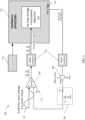
- FIG 2 depicts a block diagram of a system for measuring voltages according to one or more embodiments.
- the system 200 includes an intelligence engine 202.
- the intelligence engine 202 can be an FPGA, microcontroller, or DSP, for example.
- the intelligence engine 202 is configured to execute an AC peak voltage computation algorithm 220 which calculates an AC peak voltage of a scaled AC input voltage 210. To achieve this calculation, the intelligence engine 202 utilizes the remaining components of the system 200 that includes a comparator 204, two digital isolation circuits 216, a clock 218, a buffer 208, and an RC circuit 206.
- an AC input voltage can be received from a component on an aircraft, for example, that requires an AC voltage to be measured.
- the AC input voltage is scaled 210 before being input into the comparator 204.
- the comparator 204 compares the scaled AC input voltage 210 to a reference voltage (Vref) 212 which is a pulse width modulation (PWM) reference voltage 214 from the intelligence engine 202 after travelling through the digital isolation circuit 216, the buffer 208, and the RC circuit 206.
- Vref reference voltage
- PWM pulse width modulation
- the intelligence engine 202 can execute the AC peak voltage computation algorithm 220 which is described in further detail with reference to FIG. 3.
- FIG. 3 depicts voltage graphs at various locations in the voltage measurement system according to one or more embodiments.
- the first graph 302 shows the scaled AC input voltage (210 from FIG. 2 ) which is an input to the comparator (204 from FIG. 2 ).
- the second graph 304 shows the Vref duty cycle (214 from FIG. 2 ) which is supplied from the intelligence engine (202 from FIG. 2 ).
- the third graph 306 is the reference voltage (212 from FIG. 2 ) which is an input to the comparator (204 from FIG. 2 ).
- the fourth graph 308 shows the timing input into the intelligence engine (labeled as FPGA here).
- the intelligence sets the Vref PWM to 0% which results in the Vref being 0V inputted into the comparator 204.
- the third graph 306 shows the Vref as broken out into two parts showing a Vref1 and Vref2.
- Vref1 set at 0V in the third graph 306 gets compared to the scaled AC input voltage shown in the first graph 302. This results in the output of the comparator shown in the fourth graph 308 which is a pulse width shown as T1. This pulse width results because the comparator is comparing the positive input voltage from graph one 302 to the 0V reference voltage in graph three 306 resulting in a high output from the comparator.
- the intelligence engine 202 can calculate the line frequency F as this corresponds to a zero crossing of the input AC voltage.
- the line frequency equation is shown below as equation [1].
- Line Frequency , F 1 2 ⁇ T 1
- the output of the comparator shown in the fourth graph 308 shows the determination of frequency of the AC input voltage because for a rising edge and falling edge comparison, a width of half the duty cycle of the input voltage is shown. Hence, doubling the pulse width T1 and taking the inverse will result in the frequency.
- the VrefPWM duty cycle is set to an initial duty cycle %. As the VrefPWM signal travels through the buffer 208 and RC circuit 206, there is a charge up period as shown in graph three 306 and depicted as Vref2. Vref2 is high during the negative half cycle of the AC input voltage.
- the comparator output provides a new pulse width T2 which is lesser than the first pulse width T1.
- the difference in the two pulse widths ( ⁇ T) can be utilized for determining the input AC voltage peak by using equations 2 & 3 below.
- ⁇ T T 1 + T 2 2
- AC Voltage Peak VRE F 2 sine 2 ⁇ F ⁇ ⁇ T
- the AC Voltage peak value is calculated from equation [3] where the Vref2 from graph three 306 is known and the ⁇ T is calculated as the difference between the first pulse width T1 and the second pulse width T2.
- FIG. 4 depicts a flow diagram of a method for determining an AC voltage peak according to one or more embodiments.
- the method 400 includes providing, by a processor, a reference voltage signal to a negative input of a comparator, wherein a positive input of the comparator receives an input voltage, as shown in block 402.
- the method 400 includes setting, by the processor, the reference voltage signal to a zero voltage signal.
- the method 400 includes determining, by the processor, a line frequency of the input voltage based on a timing signal from the output of the comparator and determining a first pulse width of the input signal based on the timing signal, as shown at block 406.
- the method 400 includes setting, by the processor, the reference voltage to a pulse width modification signal with a first duty cycle. Also, the method 400, at block 410, includes receiving the timing signal from the output of the comparator. The method 400 includes determining a rising edge and a falling edge associated with the input voltage based on the timing signal, as shown at block 412. And at block 414, the method 400 includes determining a peak value of the input voltage based on a second pulse width between the rising edge and falling edge of the input voltage. The method at block 417 include setting the reference voltage to zero volts thus resulting in a 0% duty cycle. The 0% duty cycle then resets this method 400 for the reference voltage.
Landscapes
- Physics & Mathematics (AREA)
- General Physics & Mathematics (AREA)
- Nonlinear Science (AREA)
- Engineering & Computer Science (AREA)
- Power Engineering (AREA)
- Measurement Of Current Or Voltage (AREA)
Abstract
Description
- This application claims the benefit of
Indian Patent Application No. 202211016944 filed March 25, 2022 - The present invention generally relates to voltage measurements, and more specifically to, an improved accuracy for voltage measurement over extended operating conditions.
- Operating conditions on aircraft can include a temperature range between -55°C to +100°C. With these extended operating conditions, components utilized for tasks such as measuring voltages from sensors and other devices can have a higher associated costs due to the need for the component having a larger temperature operating range. For example, analog-to-digital converters (ADCs) increase in cost for larger temperature operating ranges. Designing systems for wide temperature ranges while decreasing costs can present a challenge in design. One methodology is to design systems that do not require the use of certain components that drive up the costs while maintaining accuracy of the systems.
- Embodiments of the present invention are directed to a voltage measurement system. A non-limiting example of the voltage measurement system includes a comparator having a positive input terminal and a negative input terminal, a processor configured to supply a reference voltage signal to the negative input terminal of the comparator, wherein the positive input terminal of the comparator receives an input voltage, setting the reference voltage signal to a zero voltage signal, determine a line frequency of the input voltage based on a timing signal from an output of the comparator and determining a first pulse width of the input signal based on the timing signal, set the reference voltage to a pulse width modification signal with a fixed duty cycle, receive the timing signal from the output of the comparator, determine a rising edge and a falling edge associated with the input voltage based on the timing signal, and determine a peak value of the input voltage based on a second pulse width between the rising edge and falling edge of the input voltage.
- In addition to or as an alternative to any prior system, determining the line frequency of the input voltage based on a timing signal from the output of the comparator and determining a pulse width associated with the timing signal can include: determining a second rising edge associated with the input voltage based on the timing signal; determining a second falling edge associated with the input voltage based on the timing signal; and calculating the pulse width based on an output of the comparator between the second rising edge and the second falling edge.
- In addition to or as an alternative to any prior system, determining the peak value of the input voltage based on the second pulse width between the rising edge and falling edge of the input voltage can include: determining a delta between the first pulse width and the second pulse width; and calculating the peak value of the input voltage based on the delta and the line frequency.
- In addition to or as an alternative to any prior system, the first pulse width can be larger than the second pulse width.
- In addition to or as an alternative to any prior system, the input voltage can be scaled prior to be received by the comparator.
- In addition to or as an alternative to any prior system, the input voltage can be a voltage reading taken from a component on an aircraft.
- In addition to or as an alternative to any prior system, the system can further include: a resistor capacitor (RC) circuit connected between a reference signal output of the processor and the negative input terminal of the comparator.
- In addition to or as an alternative to any prior system, the system can further include: a buffer circuit connected between the RC circuit and the reference signal output of the processor, wherein the buffer circuit includes a reference voltage supply voltage.
- In addition to or as an alternative to any prior system, the system can further include: a digital isolation circuit connected between the buffer circuit and the reference signal output of the processor.
- In addition to or as an alternative to any prior system, the system can further include: a digital isolation circuit coupled between the output of the comparator and the processor.
- Embodiments of the present invention are directed to a method. A non-limiting example of the method includes providing, by a processor, a reference voltage signal to a negative input terminal of a comparator, wherein a positive input terminal of the comparator receives an input voltage, setting, by the processor, the reference voltage signal to a zero voltage signal, determining, by the processor, a line frequency of the input voltage based on a timing signal from an output of the comparator and determining a first pulse width of the input signal based on the timing signal, setting, by the processor, the reference voltage to a pulse width modification signal with a fixed duty cycle, receiving the timing signal from the output of the comparator, determining a rising edge and a falling edge associated with the input voltage based on the timing signal, and determining a peak value of the input voltage based on a second pulse width between the rising edge and falling edge of the input voltage.
- In additional to or as an alternative to any prior method, determining the line frequency of the input voltage based on a timing signal from the output of the comparator and determining a pulse width associated with the timing signal can include: determining a second rising edge associated with the input voltage based on the timing signal; determining a second falling edge associated with the input voltage based on the timing signal; and calculating the pulse width based on an output of the comparator between the second rising edge and the second falling edge.
- In additional to or as an alternative to any prior method, determining the peak value of the input voltage based on the second pulse width between the rising edge and falling edge of the input voltage can include: determining a delta between the first pulse width and the second pulse width; and calculating the peak value of the input voltage based on the delta and the line frequency.
- In additional to or as an alternative to any prior method, the first pulse width can be larger than the second pulse width.
- In additional to or as an alternative to any prior method, the input voltage may be scaled prior to be received by the comparator.
- In additional to or as an alternative to any prior method, the input voltage may be a voltage reading taken from a component on an aircraft.
- In additional to or as an alternative to any prior method, a resistor capacitor (RC) circuit may be connected between a reference signal output of the processor and the negative input terminal of the comparator.
- In additional to or as an alternative to any prior method, a buffer circuit can be connected between the RC circuit and the reference signal output of the processor.
- In additional to or as an alternative to any prior method, a digital isolation circuit is connected between the buffer circuit and the reference signal output of the processor.
- In additional to or as an alternative to any prior method, a digital isolation circuit may be coupled between the output of the comparator and the processor.
- Additional technical features and benefits are realized through the techniques of the present invention. Embodiments and aspects of the invention are described in detail herein and are considered a part of the claimed subject matter. For a better understanding, refer to the detailed description and to the drawings.
- The specifics of the exclusive rights described herein are particularly pointed out and distinctly claimed in the claims at the conclusion of the specification. The foregoing and other features and advantages of the embodiments of the invention are apparent from the following detailed description taken in conjunction with the accompanying drawings in which:
-
FIG. 1 is a perspective view of an aircraft that may incorporate embodiments of the present disclosure; -
FIG 2 depicts a block diagram of a system for measuring voltages according to one or more embodiments; -
FIG. 3 depicts voltage graphs at various locations in the voltage measurement system according to one or more embodiments; and -
FIG. 4 depicts a flow diagram of a method for determining an AC voltage peak according to one or more embodiments. - The diagrams depicted herein are illustrative. There can be many variations to the diagram or the operations described therein without departing from the spirit of the invention. For instance, the actions can be performed in a differing order or actions can be added, deleted or modified. Also, the term "coupled" and variations thereof describes having a communications path between two elements and does not imply a direct connection between the elements with no intervening elements/connections between them. All of these variations are considered a part of the specification.
-
FIG. 1 illustrates an example of acommercial aircraft 10 havingaircraft engines 20 that may embody aspects of the teachings of this disclosure. Theaircraft 10 includes twowings 22 that each include one ormore slats 24 and one ormore flaps 26. The aircraft further includesailerons 27,spoilers 28, horizontalstabilizer trim tabs 29,rudder 30 andhorizontal stabilizer 31. The term "control surface" used herein includes but is not limited to either a slat or a flap or any of the above described. It will be understood that theslats 24 and/or theflaps 26 can include one or more slat/flap panels that move together. Theaircraft 10 also includes an system 200 (described in greater detail inFIG. 2 ) which allows AC voltage measurement without the need for analog to digital converters to be utilized for various instrumentation on board theaircraft 10. - Turning now to an overview of technologies that are more specifically relevant to aspects of the disclosure, in aircraft applications, meeting the required resolution, accuracy of AC voltage measurement over the extended operating temperature (-55°C to +100°C) can present challenges. Conventional designs for measuring an AC voltage typically use commercial off the shelf analog to digital converters (ADC) to sample and digitize an input AC voltage. For a given resolution and accuracy, selecting the correct ADC with a wide operating temperature presents challenges. Because of the need for more resolution and accuracy within these temperature ranges, AC voltage measurement systems have been utilizes premium ADC parts that have associated premium costs with fewer suppliers for supplying these premium ADC parts. Further, these premium ADC parts place a computational burden on the computational engine (e.g., FPGA, DSP, etc.) for the specified mathematical accuracy and logic consumption. Use of available premium ADCs in safety critical applications can lead to more scrutiny for verification and final certification. In many cases, the ADC will be multiplexed to measure different parameters, detecting the faults on the AC measurements some times increases ADC sampling requirements with a lower response time. Finally, one engineering practice is to design a system with dissimilar designs to meet particular safety requirements to remove common mode failures.
- Aspects of the present disclosure address the above described issues by providing a system for AC voltage measurement without using an ADC and utilizing the computational engine core capabilities. Exemplary computational engines include, but are not limited to, field programmable gate arrays (FPGAs) and digital signal processors (DSPs).
-
FIG 2 depicts a block diagram of a system for measuring voltages according to one or more embodiments. Thesystem 200 includes anintelligence engine 202. In one or more embodiments, theintelligence engine 202 can be an FPGA, microcontroller, or DSP, for example. In one or more embodiments, theintelligence engine 202 is configured to execute an AC peakvoltage computation algorithm 220 which calculates an AC peak voltage of a scaledAC input voltage 210. To achieve this calculation, theintelligence engine 202 utilizes the remaining components of thesystem 200 that includes acomparator 204, twodigital isolation circuits 216, aclock 218, abuffer 208, and anRC circuit 206. - In one or more embodiments, an AC input voltage can be received from a component on an aircraft, for example, that requires an AC voltage to be measured. The AC input voltage is scaled 210 before being input into the
comparator 204. Thecomparator 204 compares the scaledAC input voltage 210 to a reference voltage (Vref) 212 which is a pulse width modulation (PWM)reference voltage 214 from theintelligence engine 202 after travelling through thedigital isolation circuit 216, thebuffer 208, and theRC circuit 206. Thecomparator 204 converts the scaledAC input voltage 210 into a digital PWM signal. The digital PWM signal is fed into theintelligence engine 202 through anotherdigital isolation circuit 216 for further computation. - In one or more embodiments, the
intelligence engine 202 can execute the AC peakvoltage computation algorithm 220 which is described in further detail with reference toFIG. 3. FIG. 3 depicts voltage graphs at various locations in the voltage measurement system according to one or more embodiments. Thefirst graph 302 shows the scaled AC input voltage (210 fromFIG. 2 ) which is an input to the comparator (204 fromFIG. 2 ). Thesecond graph 304 shows the Vref duty cycle (214 fromFIG. 2 ) which is supplied from the intelligence engine (202 fromFIG. 2 ). Thethird graph 306 is the reference voltage (212 fromFIG. 2 ) which is an input to the comparator (204 fromFIG. 2 ). Thefourth graph 308 shows the timing input into the intelligence engine (labeled as FPGA here). In one or more embodiments, during power ON, the intelligence sets the Vref PWM to 0% which results in the Vref being 0V inputted into thecomparator 204. Thethird graph 306 shows the Vref as broken out into two parts showing a Vref1 and Vref2. Vref1 set at 0V in thethird graph 306 gets compared to the scaled AC input voltage shown in thefirst graph 302. This results in the output of the comparator shown in thefourth graph 308 which is a pulse width shown as T1. This pulse width results because the comparator is comparing the positive input voltage from graph one 302 to the 0V reference voltage in graph three 306 resulting in a high output from the comparator. In one or more embodiments, theintelligence engine 202 can calculate the line frequency F as this corresponds to a zero crossing of the input AC voltage. The line frequency equation is shown below as equation [1].
- The output of the comparator shown in the
fourth graph 308 shows the determination of frequency of the AC input voltage because for a rising edge and falling edge comparison, a width of half the duty cycle of the input voltage is shown. Hence, doubling the pulse width T1 and taking the inverse will result in the frequency. After the falling edge of the first pulse width T1, the VrefPWM duty cycle is set to an initial duty cycle %. As the VrefPWM signal travels through thebuffer 208 andRC circuit 206, there is a charge up period as shown in graph three 306 and depicted as Vref2. Vref2 is high during the negative half cycle of the AC input voltage. As the positive half cycle of the AC input voltage begins, the comparator output provides a new pulse width T2 which is lesser than the first pulse width T1. The difference in the two pulse widths (ΔT) can be utilized for determining the input AC voltage peak by usingequations 2 & 3 below.

- The AC Voltage peak value is calculated from equation [3] where the Vref2 from graph three 306 is known and the ΔT is calculated as the difference between the first pulse width T1 and the second pulse width T2.
- All the components used in this approach are COTs parts as they are easier to get in extended operating temperature range. Replacing the ADC with comparator from the demodulation approach eases the verification and certification aspects.
-
FIG. 4 depicts a flow diagram of a method for determining an AC voltage peak according to one or more embodiments. Themethod 400 includes providing, by a processor, a reference voltage signal to a negative input of a comparator, wherein a positive input of the comparator receives an input voltage, as shown inblock 402. Atblock 404, themethod 400 includes setting, by the processor, the reference voltage signal to a zero voltage signal. Also, themethod 400 includes determining, by the processor, a line frequency of the input voltage based on a timing signal from the output of the comparator and determining a first pulse width of the input signal based on the timing signal, as shown atblock 406. And, atblock 408, themethod 400 includes setting, by the processor, the reference voltage to a pulse width modification signal with a first duty cycle. Also, themethod 400, atblock 410, includes receiving the timing signal from the output of the comparator. Themethod 400 includes determining a rising edge and a falling edge associated with the input voltage based on the timing signal, as shown atblock 412. And atblock 414, themethod 400 includes determining a peak value of the input voltage based on a second pulse width between the rising edge and falling edge of the input voltage. The method at block 417 include setting the reference voltage to zero volts thus resulting in a 0% duty cycle. The 0% duty cycle then resets thismethod 400 for the reference voltage. - A detailed description of one or more embodiments of the disclosed apparatus and method are presented herein by way of exemplification and not limitation with reference to the Figures.
- The term "about" is intended to include the degree of error associated with measurement of the particular quantity based upon the equipment available at the time of filing the application.
- The terminology used herein is for the purpose of describing particular embodiments only and is not intended to be limiting of the present disclosure. As used herein, the singular forms "a", "an" and "the" are intended to include the plural forms as well, unless the context clearly indicates otherwise. It will be further understood that the terms "comprises" and/or "comprising," when used in this specification, specify the presence of stated features, integers, steps, operations, elements, and/or components, but do not preclude the presence or addition of one or more other features, integers, steps, operations, element components, and/or groups thereof.
- While the present disclosure has been described with reference to an exemplary embodiment or embodiments, it will be understood by those skilled in the art that various changes may be made and equivalents may be substituted for elements thereof without departing from the scope of the present disclosure. In addition, many modifications may be made to adapt a particular situation or material to the teachings of the present disclosure without departing from the essential scope thereof. Therefore, it is intended that the present disclosure not be limited to the particular embodiment disclosed as the best mode contemplated for carrying out this present disclosure, but that the present disclosure will include all embodiments falling within the scope of the claims.
Claims (15)
- A voltage measurement system (200) comprising:a comparator (204) having a positive input terminal and a negative input terminal;a processor (202) configured to:supply a reference voltage signal (212) to the negative input terminal of the comparator, wherein the positive input terminal of the comparator receives an input voltage (210);setting the reference voltage signal (212) to a zero voltage signal;determine a line frequency of the input voltage based on a timing signal from an output of the comparator and determining a first pulse width of the input signal based on the timing signal;set the reference voltage (212) to a pulse width modification signal with a fixed duty cycle (214);receive the timing signal from the output of the comparator;determine a rising edge and a falling edge associated with the input voltage based on the timing signal; anddetermine a peak value of the input voltage based on a second pulse width between the rising edge and falling edge of the input voltage.
- The voltage measurement system (200) of Claim 1, wherein determining the line frequency of the input voltage based on a timing signal from the output of the comparator and determining a pulse width associated with the timing signal comprises:determining a second rising edge associated with the input voltage based on the timing signal;determining a second falling edge associated with the input voltage based on the timing signal; andcalculating the pulse width based on an output of the comparator between the second rising edge and the second falling edge.
- The voltage measurement system (200) of Claim 1 or 2, wherein determining the peak value of the input voltage based on the second pulse width between the rising edge and falling edge of the input voltage comprises:determining a delta between the first pulse width and the second pulse width;
andcalculating the peak value of the input voltage based on the delta and the line frequency. - The voltage measurement system (200) of any preceding Claim, wherein the first pulse width is larger than the second pulse width.
- The voltage measurement system (200) of any preceding Claim, wherein the input voltage (210) is scaled prior to be received by the comparator.
- The voltage measurement system of any preceding Claim, wherein the input voltage is a voltage reading taken from a component on an aircraft (10).
- The voltage measurement system of any preceding Claim further comprising:
a resistor capacitor, RC, circuit (206) connected between a reference signal output of the processor and the negative input terminal of the comparator, the voltage measurement system optionally further comprising:
a buffer circuit (208) connected between the RC circuit and the reference signal output of the processor, wherein the buffer circuit includes a reference voltage supply voltage, and the voltage measurement system optionally further comprising:
a digital isolation circuit (216) connected between the buffer circuit and the reference signal output of the processor. - The voltage measurement system of any preceding Claim further comprising:
a digital isolation circuit (216) coupled between the output of the comparator and the processor. - A method (400) for measuring voltage comprising:Providing (402), by a processor, a reference voltage signal to a negative input terminal of a comparator, wherein a positive input terminal of the comparator receives an input voltage;Setting (404), by the processor, the reference voltage signal to a zero voltage signal;Determining (406), by the processor, a line frequency of the input voltage based on a timing signal from an output of the comparator and determining a first pulse width of the input signal based on the timing signal;Setting (408), by the processor, the reference voltage to a pulse width modification signal with a fixed duty cycle;receiving (410) the timing signal from the output of the comparator;determining (412) a rising edge and a falling edge associated with the input voltage based on the timing signal; anddetermining (414) a peak value of the input voltage based on a second pulse width between the rising edge and falling edge of the input voltage.
- The method of Claim 9, wherein determining the line frequency of the input voltage based on a timing signal from the output of the comparator and determining a pulse width associated with the timing signal comprises:determining a second rising edge associated with the input voltage based on the timing signal;determining a second falling edge associated with the input voltage based on the timing signal; andcalculating the pulse width based on an output of the comparator between the second rising edge and the second falling edge.
- The method of Claim 9 or 10, wherein determining the peak value of the input voltage based on the second pulse width between the rising edge and falling edge of the input voltage comprises:determining a delta between the first pulse width and the second pulse width;
andcalculating the peak value of the input voltage based on the delta and the line frequency. - The method of any of Claims 9 to 11, wherein the first pulse width is larger than the second pulse width, and/or
wherein the input voltage is scaled prior to be received by the comparator. - The method of any of Claims 9 to 12, wherein the input voltage is a voltage reading taken from a component on an aircraft.
- The method of any of Claims 9 to 13, wherein a resistor capacitor (RC) circuit is connected between a reference signal output of the processor and the negative input terminal of the comparator; optionallywherein a buffer circuit is connected between the RC circuit and the reference signal output of the processor, and further optionallywherein a digital isolation circuit is connected between the buffer circuit and the reference signal output of the processor.
- The method of any of Claims 9 to 14, wherein a digital isolation circuit is coupled between the output of the comparator and the processor.
Applications Claiming Priority (1)
| Application Number | Priority Date | Filing Date | Title |
|---|---|---|---|
| IN202211016944 | 2022-03-25 |
Publications (2)
| Publication Number | Publication Date |
|---|---|
| EP4249925A1 true EP4249925A1 (en) | 2023-09-27 |
| EP4249925B1 EP4249925B1 (en) | 2024-12-18 |
Family
ID=85726236
Family Applications (1)
| Application Number | Title | Priority Date | Filing Date |
|---|---|---|---|
| EP23163840.4A Active EP4249925B1 (en) | 2022-03-25 | 2023-03-23 | Alternative voltage measurement over extended operating conditions |
Country Status (4)
| Country | Link |
|---|---|
| US (1) | US12013420B2 (en) |
| EP (1) | EP4249925B1 (en) |
| BR (1) | BR102023005388A2 (en) |
| CA (1) | CA3193520A1 (en) |
Citations (3)
| Publication number | Priority date | Publication date | Assignee | Title |
|---|---|---|---|---|
| GB2324161A (en) * | 1997-04-09 | 1998-10-14 | Motorola Israel Ltd | Method and apparatus for detecting peaks of a signal |
| US20100073974A1 (en) * | 2008-09-19 | 2010-03-25 | Power Integrations, Inc. | Digital peak input voltage detector for a power converter controller |
| CN108490241A (en) * | 2018-05-22 | 2018-09-04 | 梧州学院 | A kind of small signal high precision peak detection device of high bandwidth |
Family Cites Families (8)
| Publication number | Priority date | Publication date | Assignee | Title |
|---|---|---|---|---|
| WO2009128006A1 (en) | 2008-04-16 | 2009-10-22 | Koninklijke Philips Electronics N.V. | Method and system for analyzing phase and amplitude information of a modulated signal |
| CN105652074B (en) * | 2014-12-03 | 2018-08-10 | 万国半导体(开曼)股份有限公司 | Voltage detecting circuit and the method for detecting voltage change |
| US10107841B2 (en) | 2015-07-24 | 2018-10-23 | Texas Instruments Incorporated | Methods and apparatus for peak-voltage measurement of AC signals |
| US9673743B1 (en) | 2016-09-08 | 2017-06-06 | Limiter Power Management System (PTY) LTD. | Efficient motor control |
| US11092464B2 (en) | 2019-01-14 | 2021-08-17 | Hamilton Sundstrand Corporation | High speed AC input sensor conversion |
| CN111142021B (en) | 2019-12-31 | 2022-01-04 | 南京航空航天大学 | Asynchronous sampling method for three-stage brushless synchronous variable frequency alternating current power generation system |
| CN112346381B (en) | 2020-10-29 | 2022-07-08 | 中国石油化工集团有限公司 | Digital phase-sensitive detection method and system based on FPGA |
| CN113495188B (en) * | 2021-06-22 | 2024-12-17 | 瀚昕微电子(无锡)有限公司 | Voltage fluctuation detection circuit |
-
2022
- 2022-05-20 US US17/749,220 patent/US12013420B2/en active Active
-
2023
- 2023-03-20 CA CA3193520A patent/CA3193520A1/en active Pending
- 2023-03-23 EP EP23163840.4A patent/EP4249925B1/en active Active
- 2023-03-23 BR BR102023005388-2A patent/BR102023005388A2/en unknown
Patent Citations (3)
| Publication number | Priority date | Publication date | Assignee | Title |
|---|---|---|---|---|
| GB2324161A (en) * | 1997-04-09 | 1998-10-14 | Motorola Israel Ltd | Method and apparatus for detecting peaks of a signal |
| US20100073974A1 (en) * | 2008-09-19 | 2010-03-25 | Power Integrations, Inc. | Digital peak input voltage detector for a power converter controller |
| CN108490241A (en) * | 2018-05-22 | 2018-09-04 | 梧州学院 | A kind of small signal high precision peak detection device of high bandwidth |
Also Published As
| Publication number | Publication date |
|---|---|
| EP4249925B1 (en) | 2024-12-18 |
| US20230305041A1 (en) | 2023-09-28 |
| BR102023005388A2 (en) | 2023-11-07 |
| US12013420B2 (en) | 2024-06-18 |
| CA3193520A1 (en) | 2023-09-25 |
Similar Documents
| Publication | Publication Date | Title |
|---|---|---|
| JP6204504B2 (en) | RF pulse synchronization, processing, and control with RF metrology | |
| EP3022737B1 (en) | Current sense circuit with offset calibration | |
| EP2863546A2 (en) | Semiconductor device and electronic control device | |
| US20150061391A1 (en) | Electronic control device | |
| US9910074B2 (en) | Digital approach to the removal of AC parasitics for impedance measurements | |
| EP2397864A1 (en) | Electricity meter and method for determining a quantity | |
| EP4249925B1 (en) | Alternative voltage measurement over extended operating conditions | |
| Kokolanski et al. | Differential inductive sensor-to-microcontroller interface circuit | |
| EP3093624B1 (en) | Self-calibrating lvdt transformer demodulator | |
| EP2687862B1 (en) | Built-in test injection for current sensing circuit | |
| WO2010136310A9 (en) | Circuit arrangement and method for temperature measurement | |
| EP3179257A1 (en) | Precise current measurement with chopping technique for high power driver | |
| US20120119763A1 (en) | Circuits and Methods for Sensing Resistance | |
| CN109923428B (en) | Apparatus and method for diagnosing multi-phase current detection | |
| JP2017053711A (en) | Control device of air-fuel ratio sensor | |
| US7813885B2 (en) | Method and apparatus for measurement of AC voltages in an HVAC system | |
| JP6588261B2 (en) | Insulation monitoring device and inverter device | |
| US10915387B2 (en) | Circuit assembly and method for monitoring a micro-controller based on a watchdog voltage | |
| US20100145652A1 (en) | Method for estimating the temperature in an internal combustion engine | |
| US20250383419A1 (en) | Calibration of integrated current sensor | |
| US10778162B1 (en) | Sensing analog signal through digital I/O pins | |
| JP2016017943A (en) | Temperature detector and temperature detector inspection method | |
| RU2610938C1 (en) | Device for magnetic fields measurement | |
| JPH0466878A (en) | Apparatus and method for measuring electrostatic capacitance, resistance and inductance | |
| JPWO2018047290A1 (en) | AC power regulator |
Legal Events
| Date | Code | Title | Description |
|---|---|---|---|
| PUAI | Public reference made under article 153(3) epc to a published international application that has entered the european phase |
Free format text: ORIGINAL CODE: 0009012 |
|
| STAA | Information on the status of an ep patent application or granted ep patent |
Free format text: STATUS: THE APPLICATION HAS BEEN PUBLISHED |
|
| AK | Designated contracting states |
Kind code of ref document: A1 Designated state(s): AL AT BE BG CH CY CZ DE DK EE ES FI FR GB GR HR HU IE IS IT LI LT LU LV MC ME MK MT NL NO PL PT RO RS SE SI SK SM TR |
|
| STAA | Information on the status of an ep patent application or granted ep patent |
Free format text: STATUS: REQUEST FOR EXAMINATION WAS MADE |
|
| 17P | Request for examination filed |
Effective date: 20240326 |
|
| RBV | Designated contracting states (corrected) |
Designated state(s): AL AT BE BG CH CY CZ DE DK EE ES FI FR GB GR HR HU IE IS IT LI LT LU LV MC ME MK MT NL NO PL PT RO RS SE SI SK SM TR |
|
| GRAP | Despatch of communication of intention to grant a patent |
Free format text: ORIGINAL CODE: EPIDOSNIGR1 |
|
| STAA | Information on the status of an ep patent application or granted ep patent |
Free format text: STATUS: GRANT OF PATENT IS INTENDED |
|
| RIC1 | Information provided on ipc code assigned before grant |
Ipc: G01R 19/25 20060101ALI20240703BHEP Ipc: G01R 19/175 20060101ALI20240703BHEP Ipc: G01R 19/04 20060101AFI20240703BHEP |
|
| INTG | Intention to grant announced |
Effective date: 20240716 |
|
| GRAS | Grant fee paid |
Free format text: ORIGINAL CODE: EPIDOSNIGR3 |
|
| GRAA | (expected) grant |
Free format text: ORIGINAL CODE: 0009210 |
|
| STAA | Information on the status of an ep patent application or granted ep patent |
Free format text: STATUS: THE PATENT HAS BEEN GRANTED |
|
| AK | Designated contracting states |
Kind code of ref document: B1 Designated state(s): AL AT BE BG CH CY CZ DE DK EE ES FI FR GB GR HR HU IE IS IT LI LT LU LV MC ME MK MT NL NO PL PT RO RS SE SI SK SM TR |
|
| REG | Reference to a national code |
Ref country code: CH Ref legal event code: EP |
|
| REG | Reference to a national code |
Ref country code: DE Ref legal event code: R096 Ref document number: 602023001376 Country of ref document: DE |
|
| REG | Reference to a national code |
Ref country code: IE Ref legal event code: FG4D |
|
| REG | Reference to a national code |
Ref country code: LT Ref legal event code: MG9D |
|
| PG25 | Lapsed in a contracting state [announced via postgrant information from national office to epo] |
Ref country code: HR Free format text: LAPSE BECAUSE OF FAILURE TO SUBMIT A TRANSLATION OF THE DESCRIPTION OR TO PAY THE FEE WITHIN THE PRESCRIBED TIME-LIMIT Effective date: 20241218 |
|
| PG25 | Lapsed in a contracting state [announced via postgrant information from national office to epo] |
Ref country code: FI Free format text: LAPSE BECAUSE OF FAILURE TO SUBMIT A TRANSLATION OF THE DESCRIPTION OR TO PAY THE FEE WITHIN THE PRESCRIBED TIME-LIMIT Effective date: 20241218 |
|
| PG25 | Lapsed in a contracting state [announced via postgrant information from national office to epo] |
Ref country code: BG Free format text: LAPSE BECAUSE OF FAILURE TO SUBMIT A TRANSLATION OF THE DESCRIPTION OR TO PAY THE FEE WITHIN THE PRESCRIBED TIME-LIMIT Effective date: 20241218 |
|
| PG25 | Lapsed in a contracting state [announced via postgrant information from national office to epo] |
Ref country code: NO Free format text: LAPSE BECAUSE OF FAILURE TO SUBMIT A TRANSLATION OF THE DESCRIPTION OR TO PAY THE FEE WITHIN THE PRESCRIBED TIME-LIMIT Effective date: 20250318 |
|
| REG | Reference to a national code |
Ref country code: NL Ref legal event code: MP Effective date: 20241218 |
|
| PG25 | Lapsed in a contracting state [announced via postgrant information from national office to epo] |
Ref country code: LV Free format text: LAPSE BECAUSE OF FAILURE TO SUBMIT A TRANSLATION OF THE DESCRIPTION OR TO PAY THE FEE WITHIN THE PRESCRIBED TIME-LIMIT Effective date: 20241218 Ref country code: GR Free format text: LAPSE BECAUSE OF FAILURE TO SUBMIT A TRANSLATION OF THE DESCRIPTION OR TO PAY THE FEE WITHIN THE PRESCRIBED TIME-LIMIT Effective date: 20250319 |
|
| PG25 | Lapsed in a contracting state [announced via postgrant information from national office to epo] |
Ref country code: RS Free format text: LAPSE BECAUSE OF FAILURE TO SUBMIT A TRANSLATION OF THE DESCRIPTION OR TO PAY THE FEE WITHIN THE PRESCRIBED TIME-LIMIT Effective date: 20250318 |
|
| PG25 | Lapsed in a contracting state [announced via postgrant information from national office to epo] |
Ref country code: NL Free format text: LAPSE BECAUSE OF FAILURE TO SUBMIT A TRANSLATION OF THE DESCRIPTION OR TO PAY THE FEE WITHIN THE PRESCRIBED TIME-LIMIT Effective date: 20241218 |
|
| REG | Reference to a national code |
Ref country code: AT Ref legal event code: MK05 Ref document number: 1752632 Country of ref document: AT Kind code of ref document: T Effective date: 20241218 |
|
| PG25 | Lapsed in a contracting state [announced via postgrant information from national office to epo] |
Ref country code: SM Free format text: LAPSE BECAUSE OF FAILURE TO SUBMIT A TRANSLATION OF THE DESCRIPTION OR TO PAY THE FEE WITHIN THE PRESCRIBED TIME-LIMIT Effective date: 20241218 |
|
| PG25 | Lapsed in a contracting state [announced via postgrant information from national office to epo] |
Ref country code: PL Free format text: LAPSE BECAUSE OF FAILURE TO SUBMIT A TRANSLATION OF THE DESCRIPTION OR TO PAY THE FEE WITHIN THE PRESCRIBED TIME-LIMIT Effective date: 20241218 |
|
| PG25 | Lapsed in a contracting state [announced via postgrant information from national office to epo] |
Ref country code: ES Free format text: LAPSE BECAUSE OF FAILURE TO SUBMIT A TRANSLATION OF THE DESCRIPTION OR TO PAY THE FEE WITHIN THE PRESCRIBED TIME-LIMIT Effective date: 20241218 |
|
| PG25 | Lapsed in a contracting state [announced via postgrant information from national office to epo] |
Ref country code: IS Free format text: LAPSE BECAUSE OF FAILURE TO SUBMIT A TRANSLATION OF THE DESCRIPTION OR TO PAY THE FEE WITHIN THE PRESCRIBED TIME-LIMIT Effective date: 20250418 |
|
| PGFP | Annual fee paid to national office [announced via postgrant information from national office to epo] |
Ref country code: IT Payment date: 20250331 Year of fee payment: 3 |
|
| PG25 | Lapsed in a contracting state [announced via postgrant information from national office to epo] |
Ref country code: PT Free format text: LAPSE BECAUSE OF FAILURE TO SUBMIT A TRANSLATION OF THE DESCRIPTION OR TO PAY THE FEE WITHIN THE PRESCRIBED TIME-LIMIT Effective date: 20250421 |
|
| PG25 | Lapsed in a contracting state [announced via postgrant information from national office to epo] |
Ref country code: EE Free format text: LAPSE BECAUSE OF FAILURE TO SUBMIT A TRANSLATION OF THE DESCRIPTION OR TO PAY THE FEE WITHIN THE PRESCRIBED TIME-LIMIT Effective date: 20241218 |
|
| PG25 | Lapsed in a contracting state [announced via postgrant information from national office to epo] |
Ref country code: AT Free format text: LAPSE BECAUSE OF FAILURE TO SUBMIT A TRANSLATION OF THE DESCRIPTION OR TO PAY THE FEE WITHIN THE PRESCRIBED TIME-LIMIT Effective date: 20241218 Ref country code: RO Free format text: LAPSE BECAUSE OF FAILURE TO SUBMIT A TRANSLATION OF THE DESCRIPTION OR TO PAY THE FEE WITHIN THE PRESCRIBED TIME-LIMIT Effective date: 20241218 |
|
| PG25 | Lapsed in a contracting state [announced via postgrant information from national office to epo] |
Ref country code: SK Free format text: LAPSE BECAUSE OF FAILURE TO SUBMIT A TRANSLATION OF THE DESCRIPTION OR TO PAY THE FEE WITHIN THE PRESCRIBED TIME-LIMIT Effective date: 20241218 |
|
| PG25 | Lapsed in a contracting state [announced via postgrant information from national office to epo] |
Ref country code: CZ Free format text: LAPSE BECAUSE OF FAILURE TO SUBMIT A TRANSLATION OF THE DESCRIPTION OR TO PAY THE FEE WITHIN THE PRESCRIBED TIME-LIMIT Effective date: 20241218 |
|
| PG25 | Lapsed in a contracting state [announced via postgrant information from national office to epo] |
Ref country code: SE Free format text: LAPSE BECAUSE OF FAILURE TO SUBMIT A TRANSLATION OF THE DESCRIPTION OR TO PAY THE FEE WITHIN THE PRESCRIBED TIME-LIMIT Effective date: 20241218 |
|
| REG | Reference to a national code |
Ref country code: DE Ref legal event code: R097 Ref document number: 602023001376 Country of ref document: DE |
|
| PG25 | Lapsed in a contracting state [announced via postgrant information from national office to epo] |
Ref country code: DK Free format text: LAPSE BECAUSE OF FAILURE TO SUBMIT A TRANSLATION OF THE DESCRIPTION OR TO PAY THE FEE WITHIN THE PRESCRIBED TIME-LIMIT Effective date: 20241218 |
|
| PG25 | Lapsed in a contracting state [announced via postgrant information from national office to epo] |
Ref country code: MC Free format text: LAPSE BECAUSE OF FAILURE TO SUBMIT A TRANSLATION OF THE DESCRIPTION OR TO PAY THE FEE WITHIN THE PRESCRIBED TIME-LIMIT Effective date: 20241218 |
|
| PLBE | No opposition filed within time limit |
Free format text: ORIGINAL CODE: 0009261 |
|
| STAA | Information on the status of an ep patent application or granted ep patent |
Free format text: STATUS: NO OPPOSITION FILED WITHIN TIME LIMIT |
|
| REG | Reference to a national code |
Ref country code: CH Ref legal event code: L10 Free format text: ST27 STATUS EVENT CODE: U-0-0-L10-L00 (AS PROVIDED BY THE NATIONAL OFFICE) Effective date: 20251029 |
|
| PG25 | Lapsed in a contracting state [announced via postgrant information from national office to epo] |
Ref country code: LU Free format text: LAPSE BECAUSE OF NON-PAYMENT OF DUE FEES Effective date: 20250323 |
|
| 26N | No opposition filed |
Effective date: 20250919 |
|
| REG | Reference to a national code |
Ref country code: BE Ref legal event code: MM Effective date: 20250331 |
|
| PG25 | Lapsed in a contracting state [announced via postgrant information from national office to epo] |
Ref country code: BE Free format text: LAPSE BECAUSE OF NON-PAYMENT OF DUE FEES Effective date: 20250331 |
|
| PG25 | Lapsed in a contracting state [announced via postgrant information from national office to epo] |
Ref country code: IE Free format text: LAPSE BECAUSE OF NON-PAYMENT OF DUE FEES Effective date: 20250323 |
|
| REG | Reference to a national code |
Ref country code: CH Ref legal event code: U11 Free format text: ST27 STATUS EVENT CODE: U-0-0-U10-U11 (AS PROVIDED BY THE NATIONAL OFFICE) Effective date: 20260401 |
|
| PGFP | Annual fee paid to national office [announced via postgrant information from national office to epo] |
Ref country code: DE Payment date: 20260320 Year of fee payment: 4 |
|
| PGFP | Annual fee paid to national office [announced via postgrant information from national office to epo] |
Ref country code: FR Payment date: 20260324 Year of fee payment: 4 |