EP4246810A1 - Clock frequency monitoring for a phase-locked loop based design - Google Patents
Clock frequency monitoring for a phase-locked loop based design Download PDFInfo
- Publication number
- EP4246810A1 EP4246810A1 EP23158272.7A EP23158272A EP4246810A1 EP 4246810 A1 EP4246810 A1 EP 4246810A1 EP 23158272 A EP23158272 A EP 23158272A EP 4246810 A1 EP4246810 A1 EP 4246810A1
- Authority
- EP
- European Patent Office
- Prior art keywords
- range
- oscillator
- frequency
- pll
- comparison range
- Prior art date
- Legal status (The legal status is an assumption and is not a legal conclusion. Google has not performed a legal analysis and makes no representation as to the accuracy of the status listed.)
- Pending
Links
Images


Classifications
-
- H—ELECTRICITY
- H03—ELECTRONIC CIRCUITRY
- H03L—AUTOMATIC CONTROL, STARTING, SYNCHRONISATION OR STABILISATION OF GENERATORS OF ELECTRONIC OSCILLATIONS OR PULSES
- H03L7/00—Automatic control of frequency or phase; Synchronisation
- H03L7/06—Automatic control of frequency or phase; Synchronisation using a reference signal applied to a frequency- or phase-locked loop
- H03L7/08—Details of the phase-locked loop
- H03L7/099—Details of the phase-locked loop concerning mainly the controlled oscillator of the loop
-
- H—ELECTRICITY
- H03—ELECTRONIC CIRCUITRY
- H03L—AUTOMATIC CONTROL, STARTING, SYNCHRONISATION OR STABILISATION OF GENERATORS OF ELECTRONIC OSCILLATIONS OR PULSES
- H03L7/00—Automatic control of frequency or phase; Synchronisation
- H03L7/06—Automatic control of frequency or phase; Synchronisation using a reference signal applied to a frequency- or phase-locked loop
- H03L7/08—Details of the phase-locked loop
- H03L7/085—Details of the phase-locked loop concerning mainly the frequency- or phase-detection arrangement including the filtering or amplification of its output signal
- H03L7/093—Details of the phase-locked loop concerning mainly the frequency- or phase-detection arrangement including the filtering or amplification of its output signal using special filtering or amplification characteristics in the loop
-
- H—ELECTRICITY
- H03—ELECTRONIC CIRCUITRY
- H03L—AUTOMATIC CONTROL, STARTING, SYNCHRONISATION OR STABILISATION OF GENERATORS OF ELECTRONIC OSCILLATIONS OR PULSES
- H03L2207/00—Indexing scheme relating to automatic control of frequency or phase and to synchronisation
- H03L2207/06—Phase locked loops with a controlled oscillator having at least two frequency control terminals
-
- H—ELECTRICITY
- H03—ELECTRONIC CIRCUITRY
- H03L—AUTOMATIC CONTROL, STARTING, SYNCHRONISATION OR STABILISATION OF GENERATORS OF ELECTRONIC OSCILLATIONS OR PULSES
- H03L2207/00—Indexing scheme relating to automatic control of frequency or phase and to synchronisation
- H03L2207/50—All digital phase-locked loop
Definitions
- This disclosure relates generally to a Phase-Locked Loop (PLL), and more specifically to monitoring an attempted alteration of a PLL generated clock.
- PLL Phase-Locked Loop
- High performance digital electronic circuits are often based on clock synchronous designs.
- registers in the design receive a clock to trigger the storage of information coming from a logic cone preceding the register.
- a logic cone represents the convergence of a multitude of signals generated synchronously at their source, which travel through logic gates to form a signal, which is synchronously latched. If the synchronous clock frequency is shortened, such that incomplete propagation occurs through the logic gates, the circuit may operate in an erroneous manner or enter an invalid state.
- a design may be maliciously attacked by attempting to alter the clock frequency of the design and thereby cause an exploitable misbehavior of the design.
- a typical countermeasure to a clock frequency attack is provided with frequency monitor, which compares the intended clock frequency to the actual modified clock frequency.
- the frequency monitor may use a second internally generated clock, which suffers from poor frequency stability and thus less accuracy in detecting a deviation of the intended clock frequency during an attack.
- Embodiments described herein provide for highly accurate clock frequency monitoring for a PLL based design, without the requirement for an additional reference clock.
- monitoring changes to the PLL derived clock prevents malicious attacks on the PLL based design caused by intentional alteration of the PLL clock or its reference frequency.
- monitoring changes to the PLL clock may also detect unintentional changes due to a variety of faults.
- the PLL based design may perform an "action" such as entering a safe operation mode (for example with a preset unlocked clock frequency and reduced design functionality).
- the action may comprise the PLL based design signaling other circuitry of a fault condition.
- a reference operating point of the PLL may be determined during a production test of the PLL based design.
- an input to oscillator is measured for a desired frequency produced by the oscillator.
- an operating point may be defined as voltage bias, current bias or digital representation thereof, which is used by an amplifier to work within the limits of a specification.
- the operating point of the oscillator is defined as a set of control settings that is needed to produce an oscillating signal with a frequency dependent upon the value of the operation point.
- the reference operating point may be represented by a capacitor bank control word.
- the reference operating point is compared to a present operating point of the PLL, determined by measuring the input to the oscillator for a desired locked frequency.
- the present operating point may be represented by a capacitor bank control word, in a similar manner to the reference operating point.
- a combination of digital gates may be configured to compare respective capacitor bank control words of the present operating to the reference operating point.
- a significant deviation of the present operating point from the reference operating point is determined when the present operating point exceeds an acceptable "range" of reference operating points, wherein the range may be determined by adding a frequency margin to the component-specific reference operating point.
- the frequency margin may be determined from a characterization of samples of the PLL based design with measurements and/or simulations performed over a range of design specific supply voltages, temperatures (e.g., a temperature of the PLL based on die or case temperature), and a process range determined from a variety of manufactured samples with shifted photo masks, dopant levels and the like.
- the determined range is relative to the reference operating point determined during production test and thus provides a range, within which the present operating point must occur for the PLL operation to be considered reliable and not subject to a malicious attack.
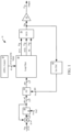
- FIG. 1 shows an example embodiment 10 of an ADPLL.
- the embodiment 10 generates a frequency at an output 12 from a reference frequency 14 and a Frequency Control Word (FCW) 16.
- FCW 16 is integrated by an adder circuit 20, adding the FCW 16 to a generated reference phase (phi_ref) 22 to produce a sum 24.
- the sum 24 is sampled with a sampling circuit 26 by the reference frequency 14 to produce the triangular-shaped reference phase 22.
- a phase detector circuit 30 produces a phase error 32 by comparing the reference phase 22 with a feedback phase word 34.
- a Loop Filter circuit 40 operates in a plurality of lock modes controlled by a signal 42 generated by an ADPLL control circuit 44.
- the loop filter circuit 40 generates lock control signals including a Process Voltage Temperature (PVT) mode signal 50, an Acquisition (ACQ) mode signal 52 and a Tracking (TR) mode signal 54.
- PVT Process Voltage Temperature
- ACQ Acquisition
- TR Tracking
- One or more of the mode control signals control a DCO 56 to produce an output signal 58.
- the output signal 58 may be buffered by a buffer 60 to produce the frequency at the output 12.
- the output signal 58 may also be fed back to the phase detector circuit 30 through a divider and/or Time to Digital Converter (TDC) 62 to form a PLL closed loop.
- TDC Time to Digital Converter
- the PVT mode signal 50 provides a locking resolution with a wide frequency range
- the ACQ mode signal 52 provides a locking resolution with a frequency range narrower than the PVT mode
- the TR mode signal 54 provides a locking resolution with a frequency range narrower than the ACQ mode.
- the PVT mode signal 50 determines whether the present operating point is within the previously defined range.
- the ACQ mode signal 52 is an intermediate mode.
- the TR mode signal 54 ensures that the ADPLL settles to a desired output frequency with jitter and/or phase noise acceptable for the intended use case. Frequency deviations within the locking limits set by the ACQ mode signal 52 and the TR mode signal 54 are within the design limits of the PLL based design and will not be sufficient to constitute a frequency attack.
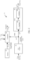
- FIG. 2 shows an example embodiment 70 of a portion of a PLL based design with further functional detail of the clock frequency monitoring.
- the PLL control circuit 76 includes the FCW integration, phase detection, ADPLL control circuit 44 and loop filter 40, while the feedback from the DCO 56 to the phase detect circuit 30 is not shown.
- the functional blocks of FIG. 2 may be physically grouped in various combinations to achieve the same function.
- the embodiment 70 includes a memory 72 to store the reference operating point of the embodiment 70 determined during a production test.
- the memory 72 also includes the range of reference operating points that the embodiment 70 is designed to operate within.
- the range may be stored in a separate memory (not shown) from the reference operating point.
- the memory may be a non-volatile memory, including but not limited to a One Time Programmable (OTP) memory.
- OTP One Time Programmable
- the memory 72 generates a digital output 74 of the reference operating point formatted as a reference capacitor bank control word.
- the definition of the range of valid cap bank control words is stored in the memory as well and provided to the comparator.
- the definition of the range is hard-coded inside the comparator.
- a PLL control circuit 76 generates a digital output 78 of the present operating point formatted as a capacitor bank control word.
- One or more of the highest order bits are connected to a net 80.
- the DCO 56 includes a capacitor bank 82 connected to the digital output 78 and an oscillator 84 controlled by the capacitor bank 82.
- the oscillator 84 provides an output frequency on the output 12.
- a comparator circuit 86 compares the reference capacitor bank control word on the digital output 74 with one or more of the highest order bits on net 80 to determine a frequency error on net 88.
- the capacitor bank control word allocates one or more highest order bits for the PVT mode 50, while the lower order bits are allocated to the ACQ 52 mode and TR mode 54.
- the comparator 86 may further include a temperature sensor input 90 and a voltage sensor input 92.
- the temperature sensor 90 measures a measured temperature of the DCO and allows for a narrowing of the range by estimating a frequency shift of the reference operating point using a predetermined temperature coefficient of the oscillator.
- the voltage sensor 92 measures a measured supply voltage of the DCO and allows for a narrowing of the range by estimating a frequency shift of the reference operating point using a predetermined voltage coefficient of the oscillator.
- the range is widened by a frequency margin proportional to a predicted temperature drift of the PLL (e.g., the embodiment 10 of FIG. 1 ).
- Other embodiments may use one or more of the temperature sensor input 90, the voltage sensor input 92 and/or the frequency margin to modify the range defined by the plurality of reference operating points.
- FIG. 3 shows a graphical view of DCO frequency characteristics relative to process, voltage and temperature variation.
- the output frequency on the output 12 is plotted against values of the reference capacitor bank control word on net 74.
- reference operating points and the resulting oscillator output frequency are measured.
- the curves 90, 92 and 94 are measured for a minimal supply voltage with an oscillator temperature of - 40C, 50C and 150C respectively.
- the curves 100, 102 and 104 are measured for a maximum supply voltage with an oscillator temperature of -40C, 50C and 150C respectively.
- the oscillator 84 is designed to operate with a nominal frequency 106 centered within a characterized and/or simulated range 108, and with a nominal reference operating point 110 measured during a production test.
- the range 108 is defined as an acceptable variation of oscillator frequencies over an acceptable variation of process, voltages and temperatures.
- the oscillator 84 may operate between the minimum and maximum reference operating points 112 and 114 respectively. Operation outside of the range 108, with a present operating point being greater than the maximum reference operating point 114 or less than the minimum reference operating point 112 may generate a frequency error on net 88 (see FIG. 2 ).
- the range 108 may be further modified with the temperature sensor input 90, the voltage sensor input 92 and/or the frequency margin.
- FIG. 4 shows an example embodiment 120 of a method for clock frequency monitoring for a PLL based design.
- a present operation point of the PLL is determined (see capacitor bank control word on net 78).
- the present operating point is compared to a range 108 defined by a plurality of reference operating points, and further defined by a process, voltage and temperature range (e.g., horizontal axis of FIG. 3 ).
- an action is performed if the present operating point (MSBs on net 80) is outside the range 108. For example, the action is performed in response to a frequency error on net 88.
- FIG. 5 shows an example embodiment 130 of another method for clock frequency monitoring for a PLL based design.
- a present operation point of the DCO 56 is determined, wherein the present operating point is defined by a capacitor bank control word (e.g., on net 78).
- the highest order bit of the present operating point e.g., one or more MSBs on net 80
- the range 108 is defined by at least one environmental factor (e.g., process, voltage, temperature or another environmental factor).
- an action is performed if the present operating point (MSBs on net 80) is outside the range 108. For example, the action is performed in response to a frequency error on net 88.
- a method for clock frequency monitoring for a Phase-Locked Loop (PLL) based design comprises determining a present operating point of an oscillator of the PLL based design, wherein the oscillator generates a present frequency in response to the present operating point.
- the present operating point of the oscillator is compared to a comparison range defined by a plurality of reference operating points, wherein the oscillator generates a nominal reference frequency in response to a nominal one of the plurality of reference operating points and the range is further defined by a manufacturing process range, an operating voltage range and an operating temperature range.
- An action is performed in response to the present operating point being outside of the comparison range.
- Alternative embodiments of the method for clock frequency monitoring for a Phase-Locked Loop (PLL) based design include one of the following features, or any combination thereof.
- the present frequency is locked with one or more lock modes, wherein each lock mode comprises a respective lock interval being less than the comparison range.
- the comparison range is narrowed with a measured temperature of the oscillator by modifying the nominal reference frequency with the measured temperature and a temperature coefficient of the oscillator.
- the comparison range is narrowed with a measured supply voltage of the oscillator by modifying the nominal reference frequency with the measured supply voltage and a voltage coefficient of the oscillator.
- the comparison range is increased by adding a frequency margin proportional to a predicted temperature drift of the PLL.
- the comparison range is determined by adding the nominal one of the plurality of reference operating points, determined by testing each PLL based design, to a frequency margin determined by characterizing a sample of PLL based designs over the manufacturing process range, the operating voltage range and the operating temperature range.
- the oscillator comprises a digitally controlled oscillator (DCO), wherein the present operating point is defined by a capacitor bank control word, and at least one highest order bit of the capacitor bank control word is compared to the comparison range.
- the range is stored in a memory.
- the memory comprises a non-volatile memory.
- an apparatus comprises a Phase-Locked Loop (PLL) based design comprising a Digitally Controlled Oscillator (DCO) configured to generate a present frequency in response to a present operating point.
- PLL Phase-Locked Loop
- DCO Digitally Controlled Oscillator
- a memory is configured to store a comparison range defined by a plurality of reference operating points, wherein the DCO is configured to generate a nominal reference frequency in response to a nominal one of the plurality of reference operating points and the comparison range is further defined by a manufacturing process range, an operating voltage range and an operating temperature range.
- a capacitor bank control word is configured to define a present operating point of the DCO.
- a controller is configured to compare at least one highest order bit of the capacitor bank control word to the comparison range and performing an action in response thereto.
- the PLL based design further comprises one or more lock modes, each comprising a respective lock interval being less than the comparison range.
- a temperature sensor is configured to measure a measured temperature of the DCO, and the controller narrows the comparison range by modifying the nominal reference frequency with the measured temperature and a temperature coefficient of the oscillator.
- a voltage sensor is configured to measure a measured supply voltage of the DCO, and the controller narrows the comparison range by modifying the nominal reference frequency with the measured supply voltage and a voltage coefficient of the oscillator.
- the comparison range comprises a frequency margin proportional to a predicted temperature drift of the PLL.
- the memory comprises a non-volatile memory.
- a digital comparator is coupled to the controller and configured to compare at least one highest order bit of the capacitor bank control word to the comparison range.
- a method for clock frequency monitoring for a Phase-Locked Loop (PLL) design comprises determining a present operating point of a digitally controlled oscillator (DCO) of the PLL based design, wherein the DCO generates a present frequency in response to the present operating point, and the present operating point is defined by a capacitor bank control word. At least one highest order bit of the capacitor bank control word is compared to a comparison range defined by a plurality of reference operating points, wherein the DCO generates a nominal reference frequency in response to a nominal one of the plurality of reference operating points and the comparison range is further defined by at least one environmental factor. An action is performed in response to the present operating point being outside of the comparison range.
- DCO digitally controlled oscillator
- Alternative embodiments of the method for clock frequency monitoring for a Phase-Locked Loop (PLL) design include one of the following features, or any combination thereof.
- the at least one environmental factor comprises at least one of an operating voltage range and an operating temperature range.
- the comparison range is narrowed with a measured temperature of the DCO by modifying the nominal reference frequency with the measured temperature and a temperature coefficient of the DCO.
- the comparison range is narrowed with a measured supply voltage of the DCO by modifying the nominal reference frequency with the measured supply voltage and a voltage coefficient of the DCO.
Landscapes
- Stabilization Of Oscillater, Synchronisation, Frequency Synthesizers (AREA)
Abstract
Description
- This disclosure relates generally to a Phase-Locked Loop (PLL), and more specifically to monitoring an attempted alteration of a PLL generated clock.
- High performance digital electronic circuits are often based on clock synchronous designs. Specifically, registers in the design receive a clock to trigger the storage of information coming from a logic cone preceding the register. A logic cone represents the convergence of a multitude of signals generated synchronously at their source, which travel through logic gates to form a signal, which is synchronously latched. If the synchronous clock frequency is shortened, such that incomplete propagation occurs through the logic gates, the circuit may operate in an erroneous manner or enter an invalid state.
- A design may be maliciously attacked by attempting to alter the clock frequency of the design and thereby cause an exploitable misbehavior of the design. A typical countermeasure to a clock frequency attack is provided with frequency monitor, which compares the intended clock frequency to the actual modified clock frequency. The frequency monitor may use a second internally generated clock, which suffers from poor frequency stability and thus less accuracy in detecting a deviation of the intended clock frequency during an attack.
- The present invention is illustrated by way of example and is not limited by the accompanying figures, in which like references indicate similar elements. Elements in the figures are illustrated for simplicity and clarity and have not necessarily been drawn to scale.
-
FIG. 1 is a schematic view of an embodiment of an All-Digital controlled Phase-Locked Loop (ADPLL). -
FIG. 2 is a schematic view of a system for clock frequency monitoring for a PLL based design, in accordance with example embodiments of the present disclosure. -
FIG. 3 is a graphical view of a Digitally Controlled Oscillator (DCO) characteristic relative to process, voltage and temperature variation, in accordance with example embodiments of the present disclosure. -
FIG. 4 is a flowchart representation of a method for clock frequency monitoring for a PLL based design, in accordance with an embodiment of the present disclosure. -
FIG. 5 is a flowchart representation of another method for clock frequency monitoring for a PLL based design, in accordance with an embodiment of the present disclosure. - Embodiments described herein provide for highly accurate clock frequency monitoring for a PLL based design, without the requirement for an additional reference clock. In some embodiments, monitoring changes to the PLL derived clock prevents malicious attacks on the PLL based design caused by intentional alteration of the PLL clock or its reference frequency. In other embodiments, monitoring changes to the PLL clock may also detect unintentional changes due to a variety of faults. Upon detection of a significant change to the PLL clock beyond design parameters, the PLL based design may perform an "action" such as entering a safe operation mode (for example with a preset unlocked clock frequency and reduced design functionality). In another embodiment, the action may comprise the PLL based design signaling other circuitry of a fault condition.
- A reference operating point of the PLL may be determined during a production test of the PLL based design. In one example, during a wafer probe or packaged component test, an input to oscillator is measured for a desired frequency produced by the oscillator. In general terms, an operating point may be defined as voltage bias, current bias or digital representation thereof, which is used by an amplifier to work within the limits of a specification. The operating point of the oscillator is defined as a set of control settings that is needed to produce an oscillating signal with a frequency dependent upon the value of the operation point. For a design based on an ADPLL, the reference operating point may be represented by a capacitor bank control word. During operation of the design, the reference operating point is compared to a present operating point of the PLL, determined by measuring the input to the oscillator for a desired locked frequency. For a design based on an ADPLL, the present operating point may be represented by a capacitor bank control word, in a similar manner to the reference operating point. In one example, a combination of digital gates may be configured to compare respective capacitor bank control words of the present operating to the reference operating point.
- A significant deviation of the present operating point from the reference operating point is determined when the present operating point exceeds an acceptable "range" of reference operating points, wherein the range may be determined by adding a frequency margin to the component-specific reference operating point. The frequency margin may be determined from a characterization of samples of the PLL based design with measurements and/or simulations performed over a range of design specific supply voltages, temperatures (e.g., a temperature of the PLL based on die or case temperature), and a process range determined from a variety of manufactured samples with shifted photo masks, dopant levels and the like. The determined range is relative to the reference operating point determined during production test and thus provides a range, within which the present operating point must occur for the PLL operation to be considered reliable and not subject to a malicious attack.
-
FIG. 1 shows anexample embodiment 10 of an ADPLL. Theembodiment 10 generates a frequency at anoutput 12 from areference frequency 14 and a Frequency Control Word (FCW) 16. The FCW 16 is integrated by anadder circuit 20, adding the FCW 16 to a generated reference phase (phi_ref) 22 to produce asum 24. Thesum 24 is sampled with asampling circuit 26 by thereference frequency 14 to produce the triangular-shaped reference phase 22. Aphase detector circuit 30 produces aphase error 32 by comparing the reference phase 22 with afeedback phase word 34. ALoop Filter circuit 40 operates in a plurality of lock modes controlled by asignal 42 generated by anADPLL control circuit 44. In one embodiment, theloop filter circuit 40 generates lock control signals including a Process Voltage Temperature (PVT) mode signal 50, an Acquisition (ACQ) mode signal 52 and a Tracking (TR) mode signal 54. One or more of the mode control signals control aDCO 56 to produce an output signal 58. The output signal 58, may be buffered by abuffer 60 to produce the frequency at theoutput 12. The output signal 58 may also be fed back to thephase detector circuit 30 through a divider and/or Time to Digital Converter (TDC) 62 to form a PLL closed loop. - In one embodiment, the PVT mode signal 50 provides a locking resolution with a wide frequency range, the ACQ mode signal 52 provides a locking resolution with a frequency range narrower than the PVT mode and the TR mode signal 54 provides a locking resolution with a frequency range narrower than the ACQ mode. The PVT mode signal 50 determines whether the present operating point is within the previously defined range. The ACQ mode signal 52 is an intermediate mode. The TR mode signal 54 ensures that the ADPLL settles to a desired output frequency with jitter and/or phase noise acceptable for the intended use case. Frequency deviations within the locking limits set by the ACQ mode signal 52 and the TR mode signal 54 are within the design limits of the PLL based design and will not be sufficient to constitute a frequency attack.
-
FIG. 2 shows anexample embodiment 70 of a portion of a PLL based design with further functional detail of the clock frequency monitoring. For ease of illustration, thePLL control circuit 76 includes the FCW integration, phase detection,ADPLL control circuit 44 andloop filter 40, while the feedback from theDCO 56 to the phase detectcircuit 30 is not shown. In other embodiments, the functional blocks ofFIG. 2 may be physically grouped in various combinations to achieve the same function. - The
embodiment 70 includes amemory 72 to store the reference operating point of theembodiment 70 determined during a production test. In one embodiment, thememory 72 also includes the range of reference operating points that theembodiment 70 is designed to operate within. In another embodiment, the range may be stored in a separate memory (not shown) from the reference operating point. In various embodiments, the memory may be a non-volatile memory, including but not limited to a One Time Programmable (OTP) memory. Thememory 72 generates adigital output 74 of the reference operating point formatted as a reference capacitor bank control word. In one embodiment the definition of the range of valid cap bank control words is stored in the memory as well and provided to the comparator. In another embodiment the definition of the range is hard-coded inside the comparator. APLL control circuit 76 generates a digital output 78 of the present operating point formatted as a capacitor bank control word. One or more of the highest order bits (e.g., Most Significant Bits) are connected to a net 80. - The DCO 56, includes a
capacitor bank 82 connected to the digital output 78 and anoscillator 84 controlled by thecapacitor bank 82. Theoscillator 84 provides an output frequency on theoutput 12. Acomparator circuit 86 compares the reference capacitor bank control word on thedigital output 74 with one or more of the highest order bits onnet 80 to determine a frequency error onnet 88. In one embodiment, the capacitor bank control word allocates one or more highest order bits for the PVT mode 50, while the lower order bits are allocated to the ACQ 52 mode and TR mode 54. Thecomparator 86 may further include atemperature sensor input 90 and avoltage sensor input 92. - In one embodiment, the
temperature sensor 90 measures a measured temperature of the DCO and allows for a narrowing of the range by estimating a frequency shift of the reference operating point using a predetermined temperature coefficient of the oscillator. In another embodiment, thevoltage sensor 92 measures a measured supply voltage of the DCO and allows for a narrowing of the range by estimating a frequency shift of the reference operating point using a predetermined voltage coefficient of the oscillator. In another embodiment, the range is widened by a frequency margin proportional to a predicted temperature drift of the PLL (e.g., theembodiment 10 ofFIG. 1 ). Other embodiments may use one or more of thetemperature sensor input 90, thevoltage sensor input 92 and/or the frequency margin to modify the range defined by the plurality of reference operating points. -
FIG. 3 shows a graphical view of DCO frequency characteristics relative to process, voltage and temperature variation. Specifically with reference toFIG. 2 , the output frequency on theoutput 12 is plotted against values of the reference capacitor bank control word onnet 74. During the characterization and/or simulation process, reference operating points and the resulting oscillator output frequency are measured. For example, thecurves curves oscillator 84 is designed to operate with a nominal frequency 106 centered within a characterized and/or simulated range 108, and with a nominal reference operating point 110 measured during a production test. The range 108 is defined as an acceptable variation of oscillator frequencies over an acceptable variation of process, voltages and temperatures. For example, theoscillator 84 may operate between the minimum and maximum reference operating points 112 and 114 respectively. Operation outside of the range 108, with a present operating point being greater than the maximumreference operating point 114 or less than the minimumreference operating point 112 may generate a frequency error on net 88 (seeFIG. 2 ). As discussed with respect toFIG. 2 , the range 108 may be further modified with thetemperature sensor input 90, thevoltage sensor input 92 and/or the frequency margin. -
FIG. 4 shows anexample embodiment 120 of a method for clock frequency monitoring for a PLL based design. With continued reference toFIG. 2 andFIG. 3 , at 122 a present operation point of the PLL is determined (see capacitor bank control word on net 78). At 124, the present operating point is compared to a range 108 defined by a plurality of reference operating points, and further defined by a process, voltage and temperature range (e.g., horizontal axis ofFIG. 3 ). At 126, an action is performed if the present operating point (MSBs on net 80) is outside the range 108. For example, the action is performed in response to a frequency error onnet 88. -
FIG. 5 shows anexample embodiment 130 of another method for clock frequency monitoring for a PLL based design. With continued reference toFIG. 2 andFIG. 3 , at 132 a present operation point of theDCO 56 is determined, wherein the present operating point is defined by a capacitor bank control word (e.g., on net 78). At 134, the highest order bit of the present operating point (e.g., one or more MSBs on net 80) is compared to the range 108. The range 108 is defined by at least one environmental factor (e.g., process, voltage, temperature or another environmental factor). At 136, an action is performed if the present operating point (MSBs on net 80) is outside the range 108. For example, the action is performed in response to a frequency error onnet 88. - As will be appreciated, at least some of the embodiments as disclosed include at least the following. In one embodiment, a method for clock frequency monitoring for a Phase-Locked Loop (PLL) based design comprises determining a present operating point of an oscillator of the PLL based design, wherein the oscillator generates a present frequency in response to the present operating point. The present operating point of the oscillator is compared to a comparison range defined by a plurality of reference operating points, wherein the oscillator generates a nominal reference frequency in response to a nominal one of the plurality of reference operating points and the range is further defined by a manufacturing process range, an operating voltage range and an operating temperature range. An action is performed in response to the present operating point being outside of the comparison range.
- Alternative embodiments of the method for clock frequency monitoring for a Phase-Locked Loop (PLL) based design include one of the following features, or any combination thereof. The present frequency is locked with one or more lock modes, wherein each lock mode comprises a respective lock interval being less than the comparison range. The comparison range is narrowed with a measured temperature of the oscillator by modifying the nominal reference frequency with the measured temperature and a temperature coefficient of the oscillator. The comparison range is narrowed with a measured supply voltage of the oscillator by modifying the nominal reference frequency with the measured supply voltage and a voltage coefficient of the oscillator. The comparison range is increased by adding a frequency margin proportional to a predicted temperature drift of the PLL. The comparison range is determined by adding the nominal one of the plurality of reference operating points, determined by testing each PLL based design, to a frequency margin determined by characterizing a sample of PLL based designs over the manufacturing process range, the operating voltage range and the operating temperature range. The oscillator comprises a digitally controlled oscillator (DCO), wherein the present operating point is defined by a capacitor bank control word, and at least one highest order bit of the capacitor bank control word is compared to the comparison range. The range is stored in a memory. The memory comprises a non-volatile memory.
- In another embodiment, an apparatus comprises a Phase-Locked Loop (PLL) based design comprising a Digitally Controlled Oscillator (DCO) configured to generate a present frequency in response to a present operating point. A memory is configured to store a comparison range defined by a plurality of reference operating points, wherein the DCO is configured to generate a nominal reference frequency in response to a nominal one of the plurality of reference operating points and the comparison range is further defined by a manufacturing process range, an operating voltage range and an operating temperature range. A capacitor bank control word is configured to define a present operating point of the DCO. A controller is configured to compare at least one highest order bit of the capacitor bank control word to the comparison range and performing an action in response thereto.
- Alternative embodiments of the apparatus include one of the following features, or any combination thereof. The PLL based design further comprises one or more lock modes, each comprising a respective lock interval being less than the comparison range. A temperature sensor is configured to measure a measured temperature of the DCO, and the controller narrows the comparison range by modifying the nominal reference frequency with the measured temperature and a temperature coefficient of the oscillator. A voltage sensor is configured to measure a measured supply voltage of the DCO, and the controller narrows the comparison range by modifying the nominal reference frequency with the measured supply voltage and a voltage coefficient of the oscillator. The comparison range comprises a frequency margin proportional to a predicted temperature drift of the PLL. The memory comprises a non-volatile memory. A digital comparator is coupled to the controller and configured to compare at least one highest order bit of the capacitor bank control word to the comparison range.
- In another embodiment, a method for clock frequency monitoring for a Phase-Locked Loop (PLL) design comprises determining a present operating point of a digitally controlled oscillator (DCO) of the PLL based design, wherein the DCO generates a present frequency in response to the present operating point, and the present operating point is defined by a capacitor bank control word. At least one highest order bit of the capacitor bank control word is compared to a comparison range defined by a plurality of reference operating points, wherein the DCO generates a nominal reference frequency in response to a nominal one of the plurality of reference operating points and the comparison range is further defined by at least one environmental factor. An action is performed in response to the present operating point being outside of the comparison range.
- Alternative embodiments of the method for clock frequency monitoring for a Phase-Locked Loop (PLL) design include one of the following features, or any combination thereof. The at least one environmental factor comprises at least one of an operating voltage range and an operating temperature range. The comparison range is narrowed with a measured temperature of the DCO by modifying the nominal reference frequency with the measured temperature and a temperature coefficient of the DCO. The comparison range is narrowed with a measured supply voltage of the DCO by modifying the nominal reference frequency with the measured supply voltage and a voltage coefficient of the DCO.
- Although the invention is described herein with reference to specific embodiments, various modifications and changes can be made without departing from the scope of the present invention as set forth in the claims below. Accordingly, the specification and figures are to be regarded in an illustrative rather than a restrictive sense, and all such modifications are intended to be included within the scope of the present invention. Any benefits, advantages, or solutions to problems that are described herein with regard to specific embodiments are not intended to be construed as a critical, required, or essential feature or element of any or all the claims.
- Unless stated otherwise, terms such as "first" and "second" are used to arbitrarily distinguish between the elements such terms describe. Thus, these terms are not necessarily intended to indicate temporal or other prioritization of such elements.
Claims (15)
- An apparatus comprising:a Phase-Locked Loop (PLL) based design comprising a Digitally Controlled Oscillator (DCO) configured to generate a present frequency in response to a present operating point;a memory configured to store a comparison range defined by a plurality of reference operating points, wherein the DCO is configured to generate a nominal reference frequency in response to a nominal one of the plurality of reference operating points and the comparison range is further defined by a manufacturing process range, an operating voltage range and an operating temperature range;a capacitor bank control word configured to define a present operating point of the DCO; anda controller configured to compare at least one highest order bit of the capacitor bank control word to the comparison range performing an action in response thereto.
- The apparatus of claim 1 wherein the PLL based design further comprises one or more lock modes, each comprising a respective lock interval being less than the comparison range.
- The apparatus of any preceding claim further comprising a temperature sensor configured to measure a temperature of the DCO, and the controller narrowing the comparison range by modifying the nominal reference frequency with the measured temperature and a temperature coefficient of the oscillator.
- The apparatus of any preceding claim further comprising a voltage sensor configured to measure a measured supply voltage of the DCO, and the controller narrowing the comparison range by modifying the nominal reference frequency with the measured supply voltage and a voltage coefficient of the oscillator.
- The apparatus of any preceding claim wherein the comparison range comprises a frequency margin proportional to a predicted temperature drift of the PLL.
- The apparatus of any preceding claim wherein the memory comprises a non-volatile memory.
- The apparatus of any preceding claim further comprising a digital comparator coupled to the controller and configured to compare at least one highest order bit of the capacitor bank control word to the comparison range.
- A method for clock frequency monitoring for a Phase-Locked Loop (PLL) based design comprising:determining a present operating point of an oscillator of the PLL based design,
wherein the oscillator generates a present frequency in response to the present operating point;comparing the present operating point of the oscillator to a comparison range defined by a plurality of reference operating points, wherein the oscillator generates a nominal reference frequency in response to a nominal one of the plurality of reference operating points and the comparison range is further defined by a manufacturing process range, an operating voltage range and an operating temperature range; andperforming an action in response to the present operating point being outside of the comparison range. - The method of claim 8 further comprising locking the present frequency with one or more lock modes, wherein each lock mode comprises a respective lock interval being less than the comparison range.
- The method of any of claims 8 to 9 wherein the comparison range is narrowed with a measured temperature of the oscillator by modifying the nominal reference frequency with the measured temperature and a temperature coefficient of the oscillator.
- The method of any of claims 8 to 10 wherein the comparison range is narrowed with a measured supply voltage of the oscillator by modifying the nominal reference frequency with the measured supply voltage and a voltage coefficient of the oscillator.
- The method of any of claims 8 to 11 wherein the comparison range is increased by adding a frequency margin proportional to a predicted temperature drift of the PLL.
- The method of any of claims 8 to 12 wherein the comparison range is determined by adding the nominal one of the plurality of reference operating points, determined by testing each PLL based design, to a frequency margin determined by characterizing a sample of PLL based designs over the manufacturing process range, the operating voltage range and the operating temperature range.
- The method of any of claims 8 to 13 wherein the oscillator comprises a digitally controlled oscillator (DCO), wherein the present operating point is defined by a capacitor bank control word, and at least one highest order bit of the capacitor bank control word is compared to the comparison range.
- The method of any of claims 8 to 15 further comprising storing the range in a memory.
Applications Claiming Priority (1)
| Application Number | Priority Date | Filing Date | Title |
|---|---|---|---|
| US17/686,664 US11689206B1 (en) | 2022-03-04 | 2022-03-04 | Clock frequency monitoring for a phase-locked loop based design |
Publications (1)
| Publication Number | Publication Date |
|---|---|
| EP4246810A1 true EP4246810A1 (en) | 2023-09-20 |
Family
ID=85381459
Family Applications (1)
| Application Number | Title | Priority Date | Filing Date |
|---|---|---|---|
| EP23158272.7A Pending EP4246810A1 (en) | 2022-03-04 | 2023-02-23 | Clock frequency monitoring for a phase-locked loop based design |
Country Status (2)
| Country | Link |
|---|---|
| US (1) | US11689206B1 (en) |
| EP (1) | EP4246810A1 (en) |
Citations (4)
| Publication number | Priority date | Publication date | Assignee | Title |
|---|---|---|---|---|
| WO2004001975A1 (en) * | 2002-06-24 | 2003-12-31 | Koninklijke Philips Electronics N.V. | Tuning system |
| US8140040B1 (en) * | 2009-09-11 | 2012-03-20 | Qualcomm Atheros, Inc | Method and apparatus for a temperature compensated phase locked loop supporting a continuous stream receiver in an integrated circuit |
| US20150077164A1 (en) * | 2013-04-30 | 2015-03-19 | Micrel, Inc. | Pll frequency synthesizer with multi-curve vco implementing closed loop curve searching using charge pump current modulation |
| US10686455B1 (en) * | 2019-08-14 | 2020-06-16 | Teledyne Defense Electronics, Llc | Digital high speed acquisition system for phase locked loops |
Family Cites Families (20)
| Publication number | Priority date | Publication date | Assignee | Title |
|---|---|---|---|---|
| US7242223B1 (en) | 2003-03-10 | 2007-07-10 | National Semiconductor Corporation | Clock frequency monitor |
| US7714665B2 (en) * | 2006-02-16 | 2010-05-11 | Texas Instruments Incorporated | Harmonic characterization and correction of device mismatch |
| WO2013070218A1 (en) * | 2011-11-09 | 2013-05-16 | Intel Corporation | Compensation for digitally controlled oscillator apparatus and method |
| US9344094B2 (en) * | 2013-03-15 | 2016-05-17 | Intel Corporation | Temperature compensated PLL calibration |
| US9762252B2 (en) * | 2013-09-16 | 2017-09-12 | Entropic Communications, Llc | Digitally controlled oscillator |
| US9337850B2 (en) * | 2014-07-30 | 2016-05-10 | Nxp, B.V. | All-digital phase-locked loop (ADPLL) with reduced settling time |
| US9350365B2 (en) * | 2014-09-18 | 2016-05-24 | Intel Corporation | Digital phase-locked loop supply voltage control |
| US9300305B1 (en) * | 2014-12-02 | 2016-03-29 | Mediatek Inc. | Frequency synthesizer and related method for improving power efficiency |
| EP3096460B1 (en) * | 2015-05-20 | 2019-11-06 | Nxp B.V. | Phase locked loop with lock detector |
| EP3190704B1 (en) * | 2016-01-06 | 2018-08-01 | Nxp B.V. | Digital phase locked loops |
| US10594323B2 (en) * | 2018-06-13 | 2020-03-17 | Movellus Circuits, Inc. | Locked loop circuit and method with digitally-controlled oscillator (DCO) gain normalization |
| US11496139B2 (en) * | 2018-06-13 | 2022-11-08 | Movellus Circuits, Inc. | Frequency measurement circuit with adaptive accuracy |
| US11070215B2 (en) * | 2018-06-13 | 2021-07-20 | Movellus Circuits, Inc. | Locked loop circuit and method with digitally-controlled oscillator (DCO) gain normalization |
| EP3641135B1 (en) * | 2018-10-17 | 2022-08-03 | NXP USA, Inc. | Frequency drift detector, communication unit and method therefor |
| EP3648352A1 (en) * | 2018-10-31 | 2020-05-06 | Stichting IMEC Nederland | Signal generator |
| US10819354B2 (en) | 2018-11-19 | 2020-10-27 | Silicon Laboratories Inc. | Accurate and reliable digital PLL lock indicator |
| US10826505B1 (en) * | 2019-06-24 | 2020-11-03 | Nxp B.V. | All digital phase locked loop (ADPLL) with frequency locked loop |
| EP3855625B1 (en) * | 2020-01-27 | 2025-07-30 | Stichting IMEC Nederland | All-digital phase locked loop and operation method thereof |
| US11218153B1 (en) * | 2020-10-29 | 2022-01-04 | Nxp B.V. | Configurable built-in self-test for an all digital phase locked loop |
| US11184013B1 (en) * | 2021-02-22 | 2021-11-23 | Infineon Technologies Ag | Digital phase-locked loop with a dynamic element matching circuit and a digitally controlled oscillator |
-
2022
- 2022-03-04 US US17/686,664 patent/US11689206B1/en active Active
-
2023
- 2023-02-23 EP EP23158272.7A patent/EP4246810A1/en active Pending
Patent Citations (4)
| Publication number | Priority date | Publication date | Assignee | Title |
|---|---|---|---|---|
| WO2004001975A1 (en) * | 2002-06-24 | 2003-12-31 | Koninklijke Philips Electronics N.V. | Tuning system |
| US8140040B1 (en) * | 2009-09-11 | 2012-03-20 | Qualcomm Atheros, Inc | Method and apparatus for a temperature compensated phase locked loop supporting a continuous stream receiver in an integrated circuit |
| US20150077164A1 (en) * | 2013-04-30 | 2015-03-19 | Micrel, Inc. | Pll frequency synthesizer with multi-curve vco implementing closed loop curve searching using charge pump current modulation |
| US10686455B1 (en) * | 2019-08-14 | 2020-06-16 | Teledyne Defense Electronics, Llc | Digital high speed acquisition system for phase locked loops |
Also Published As
| Publication number | Publication date |
|---|---|
| US11689206B1 (en) | 2023-06-27 |
Similar Documents
| Publication | Publication Date | Title |
|---|---|---|
| US7999583B2 (en) | Method and apparatus for on-chip phase error measurement to determine jitter in phase-locked loops | |
| US5745011A (en) | Data recovery phase locked loop | |
| US7372339B2 (en) | Phase lock loop indicator | |
| US11218153B1 (en) | Configurable built-in self-test for an all digital phase locked loop | |
| US20170264306A1 (en) | Compensation for digitally controlled oscillator apparatus and method | |
| US10644869B2 (en) | Automatic detection of change in PLL locking trend | |
| US7912166B2 (en) | Built-in jitter measurement circuit | |
| KR20190015062A (en) | Clock jitter measurement circuit and semiconductor device including the same | |
| US11018679B1 (en) | On-chip phase-locked loop response measurement | |
| CN108023589B (en) | Frequency calibration method and circuit | |
| US10129121B2 (en) | Clock circuit jitter calibration | |
| US6636979B1 (en) | System for measuring phase error between two clocks by using a plurality of phase latches with different respective delays | |
| US11689206B1 (en) | Clock frequency monitoring for a phase-locked loop based design | |
| US6998889B2 (en) | Circuit, apparatus and method for obtaining a lock state value | |
| KR100349482B1 (en) | Frequency measurement test circuit and semiconductor integrated circuit having the same | |
| CN106027044B (en) | A multi-loop frequency synthesizer preset frequency automatic calibration system and method | |
| US12063045B2 (en) | Feedback system monitoring | |
| US10868551B1 (en) | Non-intrusive fault detection for phase-locked loop | |
| US11190194B2 (en) | Method and apparatus for improved DPLL settling and temperature compensation algorithms using second open loop oscillator tuning field | |
| EP0881499A2 (en) | Semiconductor integrated circuit including phase locked loop circuit and jitter detector | |
| CN110824411B (en) | Parameter detection circuit and method | |
| Xia et al. | All‐digital built‐in self‐test scheme for charge‐pump phase‐locked loops | |
| US7157942B2 (en) | Digital frequency difference detector with inherent low pass filtering and lock detection | |
| CN211453930U (en) | Parameter detection circuit | |
| US20250370043A1 (en) | Bist with phase noise mitigation for measuring oscillator characteristics |
Legal Events
| Date | Code | Title | Description |
|---|---|---|---|
| PUAI | Public reference made under article 153(3) epc to a published international application that has entered the european phase |
Free format text: ORIGINAL CODE: 0009012 |
|
| STAA | Information on the status of an ep patent application or granted ep patent |
Free format text: STATUS: THE APPLICATION HAS BEEN PUBLISHED |
|
| AK | Designated contracting states |
Kind code of ref document: A1 Designated state(s): AL AT BE BG CH CY CZ DE DK EE ES FI FR GB GR HR HU IE IS IT LI LT LU LV MC ME MK MT NL NO PL PT RO RS SE SI SK SM TR |
|
| STAA | Information on the status of an ep patent application or granted ep patent |
Free format text: STATUS: REQUEST FOR EXAMINATION WAS MADE |
|
| 17P | Request for examination filed |
Effective date: 20240320 |
|
| RBV | Designated contracting states (corrected) |
Designated state(s): AL AT BE BG CH CY CZ DE DK EE ES FI FR GB GR HR HU IE IS IT LI LT LU LV MC ME MK MT NL NO PL PT RO RS SE SI SK SM TR |
|
| STAA | Information on the status of an ep patent application or granted ep patent |
Free format text: STATUS: EXAMINATION IS IN PROGRESS |
|
| 17Q | First examination report despatched |
Effective date: 20250526 |