EP4246553A1 - Process for working a wafer of 4h-sic material to form a 3c-sic layer in direct contact with the 4h-sic material - Google Patents
Process for working a wafer of 4h-sic material to form a 3c-sic layer in direct contact with the 4h-sic material Download PDFInfo
- Publication number
- EP4246553A1 EP4246553A1 EP23160409.1A EP23160409A EP4246553A1 EP 4246553 A1 EP4246553 A1 EP 4246553A1 EP 23160409 A EP23160409 A EP 23160409A EP 4246553 A1 EP4246553 A1 EP 4246553A1
- Authority
- EP
- European Patent Office
- Prior art keywords
- sic
- layer
- wafer
- process according
- silicon layer
- Prior art date
- Legal status (The legal status is an assumption and is not a legal conclusion. Google has not performed a legal analysis and makes no representation as to the accuracy of the status listed.)
- Granted
Links
Images


Classifications
-
- H—ELECTRICITY
- H10—SEMICONDUCTOR DEVICES; ELECTRIC SOLID-STATE DEVICES NOT OTHERWISE PROVIDED FOR
- H10P—GENERIC PROCESSES OR APPARATUS FOR THE MANUFACTURE OR TREATMENT OF DEVICES COVERED BY CLASS H10
- H10P14/00—Formation of materials, e.g. in the shape of layers or pillars
- H10P14/20—Formation of materials, e.g. in the shape of layers or pillars of semiconductor materials
- H10P14/34—Deposited materials, e.g. layers
- H10P14/3402—Deposited materials, e.g. layers characterised by the chemical composition
- H10P14/3404—Deposited materials, e.g. layers characterised by the chemical composition being Group IVA materials
- H10P14/3408—Silicon carbide
-
- H—ELECTRICITY
- H10—SEMICONDUCTOR DEVICES; ELECTRIC SOLID-STATE DEVICES NOT OTHERWISE PROVIDED FOR
- H10P—GENERIC PROCESSES OR APPARATUS FOR THE MANUFACTURE OR TREATMENT OF DEVICES COVERED BY CLASS H10
- H10P14/00—Formation of materials, e.g. in the shape of layers or pillars
- H10P14/20—Formation of materials, e.g. in the shape of layers or pillars of semiconductor materials
- H10P14/29—Formation of materials, e.g. in the shape of layers or pillars of semiconductor materials characterised by the substrates
- H10P14/2901—Materials
- H10P14/2902—Materials being Group IVA materials
- H10P14/2904—Silicon carbide
-
- H—ELECTRICITY
- H10—SEMICONDUCTOR DEVICES; ELECTRIC SOLID-STATE DEVICES NOT OTHERWISE PROVIDED FOR
- H10P—GENERIC PROCESSES OR APPARATUS FOR THE MANUFACTURE OR TREATMENT OF DEVICES COVERED BY CLASS H10
- H10P14/00—Formation of materials, e.g. in the shape of layers or pillars
- H10P14/20—Formation of materials, e.g. in the shape of layers or pillars of semiconductor materials
-
- H—ELECTRICITY
- H10—SEMICONDUCTOR DEVICES; ELECTRIC SOLID-STATE DEVICES NOT OTHERWISE PROVIDED FOR
- H10P—GENERIC PROCESSES OR APPARATUS FOR THE MANUFACTURE OR TREATMENT OF DEVICES COVERED BY CLASS H10
- H10P14/00—Formation of materials, e.g. in the shape of layers or pillars
- H10P14/20—Formation of materials, e.g. in the shape of layers or pillars of semiconductor materials
- H10P14/32—Formation of materials, e.g. in the shape of layers or pillars of semiconductor materials characterised by intermediate layers between substrates and deposited layers
- H10P14/3202—Materials thereof
- H10P14/3204—Materials thereof being Group IVA semiconducting materials
- H10P14/3208—Silicon carbide
-
- H—ELECTRICITY
- H10—SEMICONDUCTOR DEVICES; ELECTRIC SOLID-STATE DEVICES NOT OTHERWISE PROVIDED FOR
- H10P—GENERIC PROCESSES OR APPARATUS FOR THE MANUFACTURE OR TREATMENT OF DEVICES COVERED BY CLASS H10
- H10P14/00—Formation of materials, e.g. in the shape of layers or pillars
- H10P14/20—Formation of materials, e.g. in the shape of layers or pillars of semiconductor materials
- H10P14/32—Formation of materials, e.g. in the shape of layers or pillars of semiconductor materials characterised by intermediate layers between substrates and deposited layers
- H10P14/3202—Materials thereof
- H10P14/3204—Materials thereof being Group IVA semiconducting materials
- H10P14/3211—Silicon, silicon germanium or germanium
-
- H—ELECTRICITY
- H10—SEMICONDUCTOR DEVICES; ELECTRIC SOLID-STATE DEVICES NOT OTHERWISE PROVIDED FOR
- H10P—GENERIC PROCESSES OR APPARATUS FOR THE MANUFACTURE OR TREATMENT OF DEVICES COVERED BY CLASS H10
- H10P14/00—Formation of materials, e.g. in the shape of layers or pillars
- H10P14/20—Formation of materials, e.g. in the shape of layers or pillars of semiconductor materials
- H10P14/32—Formation of materials, e.g. in the shape of layers or pillars of semiconductor materials characterised by intermediate layers between substrates and deposited layers
- H10P14/3242—Structure
- H10P14/3244—Layer structure
- H10P14/3248—Layer structure consisting of two layers
-
- H—ELECTRICITY
- H10—SEMICONDUCTOR DEVICES; ELECTRIC SOLID-STATE DEVICES NOT OTHERWISE PROVIDED FOR
- H10P—GENERIC PROCESSES OR APPARATUS FOR THE MANUFACTURE OR TREATMENT OF DEVICES COVERED BY CLASS H10
- H10P14/00—Formation of materials, e.g. in the shape of layers or pillars
- H10P14/20—Formation of materials, e.g. in the shape of layers or pillars of semiconductor materials
- H10P14/34—Deposited materials, e.g. layers
- H10P14/3402—Deposited materials, e.g. layers characterised by the chemical composition
- H10P14/3404—Deposited materials, e.g. layers characterised by the chemical composition being Group IVA materials
- H10P14/3406—Carbon, e.g. diamond-like carbon
-
- H—ELECTRICITY
- H10—SEMICONDUCTOR DEVICES; ELECTRIC SOLID-STATE DEVICES NOT OTHERWISE PROVIDED FOR
- H10P—GENERIC PROCESSES OR APPARATUS FOR THE MANUFACTURE OR TREATMENT OF DEVICES COVERED BY CLASS H10
- H10P14/00—Formation of materials, e.g. in the shape of layers or pillars
- H10P14/20—Formation of materials, e.g. in the shape of layers or pillars of semiconductor materials
- H10P14/38—Formation of materials, e.g. in the shape of layers or pillars of semiconductor materials characterised by treatments done after the formation of the materials
- H10P14/3802—Crystallisation or recrystallisation of non-monocrystalline semiconductor materials, e.g. regrowth
- H10P14/3808—Crystallisation or recrystallisation of non-monocrystalline semiconductor materials, e.g. regrowth using laser beams
-
- H—ELECTRICITY
- H10—SEMICONDUCTOR DEVICES; ELECTRIC SOLID-STATE DEVICES NOT OTHERWISE PROVIDED FOR
- H10P—GENERIC PROCESSES OR APPARATUS FOR THE MANUFACTURE OR TREATMENT OF DEVICES COVERED BY CLASS H10
- H10P14/00—Formation of materials, e.g. in the shape of layers or pillars
- H10P14/20—Formation of materials, e.g. in the shape of layers or pillars of semiconductor materials
- H10P14/38—Formation of materials, e.g. in the shape of layers or pillars of semiconductor materials characterised by treatments done after the formation of the materials
- H10P14/3802—Crystallisation or recrystallisation of non-monocrystalline semiconductor materials, e.g. regrowth
- H10P14/3808—Crystallisation or recrystallisation of non-monocrystalline semiconductor materials, e.g. regrowth using laser beams
- H10P14/3816—Pulsed laser beam
-
- H—ELECTRICITY
- H10—SEMICONDUCTOR DEVICES; ELECTRIC SOLID-STATE DEVICES NOT OTHERWISE PROVIDED FOR
- H10P—GENERIC PROCESSES OR APPARATUS FOR THE MANUFACTURE OR TREATMENT OF DEVICES COVERED BY CLASS H10
- H10P14/00—Formation of materials, e.g. in the shape of layers or pillars
- H10P14/60—Formation of materials, e.g. in the shape of layers or pillars of insulating materials
- H10P14/69—Inorganic materials
- H10P14/692—Inorganic materials composed of oxides, glassy oxides or oxide-based glasses
- H10P14/6921—Inorganic materials composed of oxides, glassy oxides or oxide-based glasses containing silicon
- H10P14/69215—Inorganic materials composed of oxides, glassy oxides or oxide-based glasses containing silicon the material being a silicon oxide, e.g. SiO2
-
- H—ELECTRICITY
- H10—SEMICONDUCTOR DEVICES; ELECTRIC SOLID-STATE DEVICES NOT OTHERWISE PROVIDED FOR
- H10P—GENERIC PROCESSES OR APPARATUS FOR THE MANUFACTURE OR TREATMENT OF DEVICES COVERED BY CLASS H10
- H10P50/00—Etching of wafers, substrates or parts of devices
- H10P50/60—Wet etching
- H10P50/64—Wet etching of semiconductor materials
- H10P50/642—Chemical etching
Definitions
- the present invention relates to a process for working a 4H-SiC wafer, in order to form a layer with a reduced bandgap with respect to 4H-SiC, such as for example a 3C-SiC or Silicon layer, on the 4H-SiC wafer.
- SiC silicon carbide
- an advantage associated with the manufacturing of a device on a substrate (bulk) of 4H-SiC is maintaining the advantage in breakdown voltage, but having on the surface a material that has a lower bandgap (for example, silicon or 3C-SiC), so as to have a reduction of the barrier height, for example, of the Schottky contact.
- a material that has a lower bandgap for example, silicon or 3C-SiC
- Silicon carbide comes in different crystalline forms, also called polytypes.
- the most common polytypes are the cubic polytype (polytype 3C-SiC), the hexagonal polytype (polytypes 4H-SiC and 6H-SiC) and the rhombohedral polytype (polytype 15R-SiC).
- the cubic polytype 3C-SiC is currently being studied in depth, owing to its unique properties compared to other wafer polytypes.
- the polytype 3C-SiC offers several advantages for Metal Oxide Semiconductor (MOS) device applications, for example it may help increase drift mobility with its reduced Oxide/3C-SiC interface trap density.
- MOS Metal Oxide Semiconductor
- the reduced bandgap of 3C-SiC helps reduce the electric field strength necessary to obtain the channel inversion.
- Other characteristics that make 3C-SiC interesting consist in the low value of the on-state resistance Ron, particularly useful in case of devices that work up to and over 650 V.
- 4H-SiC is commonly used as a substrate.
- the bandgap of 4H-SiC is greater (3.2 eV) with respect to the corresponding bandgap of 3C-SiC (2.3 eV) or Silicon (1.12 eV), making 4H-SiC less attractive for some electronic applications with respect to 3C-SiC or with respect to Silicon.
- SBH Schottky Barrier Height
- the implementation of metal/3C-SiC or metal/Si contacts entails lower SBH values with respect to the SBH values of metal/4H-SiC contacts, enabling the manufacturing of more efficient Schottky diodes.
- VLS Vapor-Liquid-Solid
- SE Sublimation Epitaxy
- the above-mentioned methods require a plurality of growth steps and a high control of the surface morphology (especially as regards the layers, or films, grown with the SE method on an off-axis 4H-SiC substrate).
- 3C-SiC layer An alternative to the techniques discussed above for manufacturing a 3C-SiC layer is chemical vapor deposition (CVD) on a Silicon substrate.
- CVD chemical vapor deposition
- the 3C-SiC layers thus formed have a high defect density (in the order of 10 8 -10 9 per cm 2 , which results from about 20% of lattice mismatching between the two materials).
- the aim of the present invention is to provide a process for working a 4H-SiC wafer in such a way as to overcome the drawbacks and limitations of the prior art.
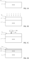
- Figures 1A-1F a method for forming a silicon carbide layer of the polytype 3C-SiC according to an embodiment of the present invention is illustrated and described.
- Figures 1A-1F are represented in a triaxial reference system of X, Y, Z axes orthogonal to each other.
- a wafer 1 of silicon carbide of the polytype 4H-SiC, particularly crystalline 4H-SiC, even more particularly single-crystal 4H-SiC, is provided.
- the wafer 1 includes a front side 1a and a rear side 1b, opposite to each other along the Z axis.
- the wafer 1 has, in one embodiment, a first electrical conductivity type, for example an N-type conductivity, and doping in the range 10 18 -10 22 atoms/cm 3 .
- the wafer 1 has, for example, a thickness, measured along the Z axis, equal to about 100 - 400 um.
- the present invention applies to any 4H-SiC substrate.
- the wafer 1 has a different conductivity (i.e. of a P-type).
- the conductivity or starting doping type of the wafer 1 is not relevant.
- the wafer 1 is manufactured in a per se known manner and is not an object of the present invention.
- 4H-SiC wafers are commercially available.
- an implant (identified by arrows 2, parallel to the Z axis) step of doping species is performed.
- the implant occurs at the front side 1a and is performed in the absence of an implant mask (the use of an implant mask may still be provided, based on the needs and design choices).
- a doped layer 3 is thus formed which extends uniformly at the front side 1a.
- the doped layer 3 extends in depth into the wafer 1, and reaches a maximum depth comprised between 100 nm and 1000 nm, measured from the surface of the front side 1a.
- the doping step of Figure 1B may provide, in one embodiment, a doping with doping species having the first electrical conductivity (N), for example nitrogen (N) and phosphorus (P).
- the implant is performed with implant energy comprised between 20 and 500 keV and with doses between 10 14 and 10 16 atoms/cm 2 , to form the doped layer 3 with a dopant concentration comprised between 10 17 and 10 20 atoms/cm 3 .
- the doping step of Figure 1B may provide, in a different embodiment, a doping with doping species having a second electrical conductivity (P) opposite to the first conductivity, for example Aluminum.
- the implant is performed with implant energy comprised between 20 and 500 keV and with doses between 10 14 and 10 16 atoms/cm 2 , to form the doped layer 3 with a dopant concentration comprised between 10 17 and 10 20 atoms/cm 3 .
- the implant step "breaks" the crystalline structure of 4H-SiC, making the melting step described hereinbelow performable at lower temperatures with respect to the case of crystalline material (as for example in the case described at Figure 3B ).
- a thermal budget is generated at the surface of the front side 1a for causing a local melt of a portion of the wafer 1 at the front side 1a.
- a LASER source 100 is used configured to generate a beam 102 such that it heats the front side 1a, and in particular the doped layer 3, up to a temperature comprised between about 1600 °C and 3000 °C. Given the maximum depth reached by the doped layer 3, a temperature of about 2000°C at the level of the surface of the front side 1a is sufficient to ensure temperatures within the range identified above even at the maximum depth reached by the doped layer 3.
- This temperature is, as said, such that it causes the melting of the doped layer 3; by interrupting the generation of the beam 102, that is interrupting the heating of the wafer 1, the re-solidification of the portions previously being melted and a crystallization thereof are observed.
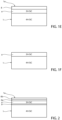
- the Applicant has observed that the crystallization of the wafer 1 generates a plurality of superimposed layers, including a 3C-SiC layer 4 on the 4H-SiC material not being melted, a silicon layer 6a on the 3C-SiC layer 4 and one or more carbon-rich layers 6b (comprising for example one or more graphite layers and/or one or more graphene layers) on the silicon layer 6a, as illustrated in Figure 1D .
- the transformation of the doped layer 3 into layers 4, 6a and 6b occurs by heating the entire front side 1a of the wafer 1, suitably moving the LASER 100.
- a plurality of scannings of the LASER 100 are carried out on the XY plane (e.g., a plurality of scannings parallel to each other and to the X axis and/or Y axis).
- only a predefined portion of the doped layer 3 is processed by LASER 100, to obtain the formation of the 3C-SiC layer exclusively in some regions of the wafer 1 and not in others (for example only at regions wherein there will be formed active areas of devices which are intended to be provided/integrated in the wafer 1).
- the LASER 100 is, for example, an excimer UV LASER. Other types of LASERs may be used, including LASERs with wavelength in the region of the visible.
- the configuration and operating parameters of the LASER 100 optimized to achieve the aim of the present invention according to the embodiment of Figures 1A-1D , are the following:
- the area of the spot of the beam 102 at the level of the front side 1a is, for example, comprised between 0.7 and 1.5 cm 2 .
- the crystallization of the portion(s) being melted occurs in an environment with a temperature comprised between 1600 °C and 2700 °C, in a time comprised between 100 ns and 300 ns.
- an oxidation step of the carbon-rich layer 6b and of the underlying silicon layer 6a is performed, forming respective oxidized layers (indicated together with the reference 8 in Figure 1E ).
- This step is performed by inserting the wafer 1 into a furnace at a temperature of 800 °C for 60 min in an oxidizing environment, such as for example an oxygen-rich atmosphere. This favors the oxidation of both the carbon-rich layer and the silicon layer.
- an oxidizing environment such as for example an oxygen-rich atmosphere.
- the etching chemical solution selectively removes the material of the oxidized layers 8, the etching proceeds up to complete removal of the oxidized layers 8, without removing the underlying 3C-SiC layer 4.
- the formation of the 6H-SiC layer is caused by a suitable choice of the thermal budget that is provided to the 4H-SiC wafer through the LASER 100, that is by adjusting the configuration and operating parameters of the LASER 100 during the melting step of the portion of the wafer being processed.
- the subsequent crystallization of the melted portion leads, in a natural manner (i.e., not mediated by a further intervention by the operator), to the additional formation of the 6H-SiC layer.
- the configuration/operating parameters of the LASER 100 i.e., of the radiation emitted by the LASER) are the following:
- the crystallization of the portion(s) being melted occurs in an environment with a temperature comprised between 1600 °C and 2700 °C, in a time comprised between 100 ns and 300 ns.
- Figures 3A-3E illustrate a further embodiment of the present invention.
- Figures 3A-3E are depicted in a triaxial reference system of X, Y, Z axes orthogonal to each other.
- a wafer 21 of silicon carbide of the polytype 4H-SiC, particularly crystalline 4H-SiC, even more particularly single-crystal 4H-SiC, is provided.
- the wafer 21 includes a front side 21a and a rear side 21b, opposite to each other along the Z axis.
- the wafer 21 has, in one embodiment, a first electrical conductivity type, for example an N-type conductivity, and doping in the range 1e18-1e22 atoms/cm 3 .
- the wafer 21 has, for example, a thickness, measured along the Z axis, equal to about 100 and 400 um.
- the wafer 21 has a different conductivity (i.e. of a P-type).
- the conductivity or starting doping type of the wafer 21 is not relevant.
- the wafer 1 is manufactured in a per se known manner and is not an object of the present invention.
- 4H-SiC wafers are commercially available.
- the LASER source 100 is used, configured to generate the beam 102 for heating the front side 21a up to a temperature equal to about 1600-3000 °C.
- a temperature of about 3000°C at the level of the surface of the front side 21a is sufficient to ensure temperatures within the range identified above in depth in the wafer 21, for example equal to about 10 um. This temperature is such that it causes a melting of the portions of the wafer 21 being processed through LASER 100.
- the Applicant has observed that the crystallization of the wafer 21 generates a plurality of superimposed layers, including a 3C-SiC layer 24 on the 4H-SiC material not being melted, a silicon layer 26a on the 3C-SiC layer 24 and one or more carbon-rich layers 26b (including for example graphite layers, or graphene multi-layers) on the silicon layer 26a, as illustrated in Figure 3C .
- the transformation of portions of the wafer 1 into layers 24, 26a and 26b occurs by heating the entire front side 21a of the wafer 21, suitably moving the LASER 100.
- a plurality of scannings of the LASER 100 are carried out on the XY plane (e.g., a plurality of scannings parallel to each other and to the X axis and/or Y axis).
- only some regions (in XY plane top view) of the wafer 1 are processed by LASER 100, to obtain the formation of the 3C-SiC layer 24 exclusively in some regions of the wafer 21 and not in others (for example only at regions wherein there will be formed active areas of devices which are intended to be provided/integrated in the wafer 21).
- the configuration and operating parameters of the LASER 100 optimized to achieve the aim of the present invention according to the embodiment of Figures 3A-3C , are the following:
- the area of the spot of the beam 102 at the level of the front side 1a is, for example, comprised between 0.7 and 1.5 cm 2 .
- the crystallization of the portion(s) being melted occurs in an environment with a temperature comprised between 1600 and 2700 °C, in a time comprised between 100 ns and 300 ns.
- This step is performed by inserting the wafer 21 into a furnace at a temperature of 800 °C for 60 min in an oxidizing environment and, in particular, in an oxygen environment. This favors the oxidation of both the carbon-rich layer and the silicon layer. The Applicant has not observed a corresponding oxidation of the 3C-SiC layer and of the 4H-SiC substrate.
- the etching chemical solution selectively removes the material of the oxidized layers 28, the etching proceeds up to complete removal of the same, without removing the underlying 3C-SiC layer 24.
- the formation of the 6H-SiC layer 29 is caused (as already discussed with reference to Figure 2 ) by suitably adjusting the configuration and operating parameters of the LASER 100, for the emission of a suitable beam, as follows:
- the crystallization of the portion(s) being melted occurs in an environment with a temperature comprised between 1600 °C and 2700 °C, in a time comprised between 100 ns and 300 ns.
- the Applicant has verified that the 3C-SiC layer thus manufactured has a low defect density.
- the heating and melting process occurs in a single step, during which it is possible to accurately control the LASER parameters (for example in terms of energy and number of pulses), making the process highly reproducible.
Landscapes
- Crystals, And After-Treatments Of Crystals (AREA)
- Chemical & Material Sciences (AREA)
- Chemical Kinetics & Catalysis (AREA)
- General Chemical & Material Sciences (AREA)
- Physics & Mathematics (AREA)
- Optics & Photonics (AREA)
- Recrystallisation Techniques (AREA)
Abstract
Description
- The present invention relates to a process for working a 4H-SiC wafer, in order to form a layer with a reduced bandgap with respect to 4H-SiC, such as for example a 3C-SiC or Silicon layer, on the 4H-SiC wafer.
- As known, semiconductor devices are typically manufactured in silicon wafers. However, silicon carbide (SiC) wafers have become increasingly popular owing, at least in part, to the favorable physico-chemical properties of SiC. For example, SiC generally has a higher bandgap with respect to silicon, with the consequence of obtaining a greater barrier height when, for example, a Schottky contact is formed. Moreover, the breakdown voltage of SiC is also greater than that of silicon. This is due to the fact that the critical electric field of SiC is about ten times greater than that of silicon. In general, an advantage associated with the manufacturing of a device on a substrate (bulk) of 4H-SiC is maintaining the advantage in breakdown voltage, but having on the surface a material that has a lower bandgap (for example, silicon or 3C-SiC), so as to have a reduction of the barrier height, for example, of the Schottky contact. In other words, maintaining the advantage in reverse bias and optimizing the voltage drop in forward bias is desirable.
- Silicon carbide comes in different crystalline forms, also called polytypes. The most common polytypes are the cubic polytype (polytype 3C-SiC), the hexagonal polytype (
polytypes 4H-SiC and 6H-SiC) and the rhombohedral polytype (polytype 15R-SiC). Among these, the cubic polytype 3C-SiC is currently being studied in depth, owing to its unique properties compared to other wafer polytypes. The polytype 3C-SiC offers several advantages for Metal Oxide Semiconductor (MOS) device applications, for example it may help increase drift mobility with its reduced Oxide/3C-SiC interface trap density. The reduced bandgap of 3C-SiC helps reduce the electric field strength necessary to obtain the channel inversion. Other characteristics that make 3C-SiC interesting consist in the low value of the on-state resistance Ron, particularly useful in case of devices that work up to and over 650 V. - For the greater ease of manufacture with respect to other polytypes, 4H-SiC is commonly used as a substrate. However, the bandgap of 4H-SiC is greater (3.2 eV) with respect to the corresponding bandgap of 3C-SiC (2.3 eV) or Silicon (1.12 eV), making 4H-SiC less attractive for some electronic applications with respect to 3C-SiC or with respect to Silicon. For example, in case of Schottky barrier diodes, the possibility of controlling the Schottky Barrier Height (SBH) is an important aspect in order to reduce energy consumption and minimize conduction losses. To this end, the implementation of metal/3C-SiC or metal/Si contacts entails lower SBH values with respect to the SBH values of metal/4H-SiC contacts, enabling the manufacturing of more efficient Schottky diodes.
- Different methods have been proposed for growing cubic silicon carbide (3C-SiC) on a hexagonal silicon carbide (4H-SiC or 6H-SiC) substrate. One of these is known as Vapor-Liquid-Solid (VLS) mechanism, for example described by Soueidan M. et al., "A Vapor-Liquid-Solid Mechanism for Growing 3C-SiC Single-Domain Layers on 6H-SiC (0001)", Advanced Functional Materials, vol. 16, pages 975-979, 02 May 2006.
- Another method is known as Sublimation Epitaxy (SE).
- However, the above-mentioned methods require a plurality of growth steps and a high control of the surface morphology (especially as regards the layers, or films, grown with the SE method on an off-
axis 4H-SiC substrate). - An alternative to the techniques discussed above for manufacturing a 3C-SiC layer is chemical vapor deposition (CVD) on a Silicon substrate. However, the 3C-SiC layers thus formed have a high defect density (in the order of 108-109 per cm2, which results from about 20% of lattice mismatching between the two materials).
- Other solutions have also been proposed, such as for example the heteroepitaxial growth of 3C-SiC on an in-axis 6H-SiC substrate, for example by CVD technique or by sublimation. However, the high number of parameters to be set to obtain a final product having good quality and the numerous variables that affect the formation of the 3C-SiC layer, limit the use of known methods, especially in the industrial and mass production fields.
- The aim of the present invention is to provide a process for working a 4H-SiC wafer in such a way as to overcome the drawbacks and limitations of the prior art.
- According to the present invention a process for working a 4H-SiC wafer is provided as defined in the attached claims.
- For a better understanding of the present invention, preferred embodiments thereof are now described, purely by way of non-limiting example, with reference to the attached drawings, wherein:
-
Figures 1A-1F illustrate successive steps of a process for manufacturing a 3C-SiC layer, according to an embodiment of the present invention; -
Figure 2 illustrates a step of a process for manufacturing a 3C-SiC layer, according to a further embodiment of the present invention; -
Figures 3A-3E illustrate successive steps of a process for manufacturing a 3C-SiC layer, according to a further embodiment of the present invention; and -
Figure 4 illustrates a step of a process for manufacturing a 3C-SiC layer, according to a further embodiment of the present invention. - With reference to
Figures 1A-1F , a method for forming a silicon carbide layer of the polytype 3C-SiC according to an embodiment of the present invention is illustrated and described.Figures 1A-1F are represented in a triaxial reference system of X, Y, Z axes orthogonal to each other. - With reference to
Figure 1A , awafer 1 of silicon carbide of thepolytype 4H-SiC, particularly crystalline 4H-SiC, even more particularly single-crystal 4H-SiC, is provided. Thewafer 1 includes afront side 1a and a rear side 1b, opposite to each other along the Z axis. Thewafer 1 has, in one embodiment, a first electrical conductivity type, for example an N-type conductivity, and doping in the range 1018-1022 atoms/cm3. Thewafer 1 has, for example, a thickness, measured along the Z axis, equal to about 100 - 400 um. - In general, the present invention applies to any 4H-SiC substrate.
- In a further embodiment, the
wafer 1 has a different conductivity (i.e. of a P-type). However, for the purposes of the present invention, the conductivity or starting doping type of thewafer 1 is not relevant. - The
wafer 1 is manufactured in a per se known manner and is not an object of the present invention. However, 4H-SiC wafers are commercially available. - With reference to
Figure 1B , an implant (identified by arrows 2, parallel to the Z axis) step of doping species is performed. The implant occurs at thefront side 1a and is performed in the absence of an implant mask (the use of an implant mask may still be provided, based on the needs and design choices). - A doped
layer 3 is thus formed which extends uniformly at thefront side 1a. The dopedlayer 3 extends in depth into thewafer 1, and reaches a maximum depth comprised between 100 nm and 1000 nm, measured from the surface of thefront side 1a. - The doping step of
Figure 1B may provide, in one embodiment, a doping with doping species having the first electrical conductivity (N), for example nitrogen (N) and phosphorus (P). The implant is performed with implant energy comprised between 20 and 500 keV and with doses between 1014 and 1016 atoms/cm2, to form the dopedlayer 3 with a dopant concentration comprised between 1017 and 1020 atoms/cm3. - The doping step of
Figure 1B may provide, in a different embodiment, a doping with doping species having a second electrical conductivity (P) opposite to the first conductivity, for example Aluminum. The implant is performed with implant energy comprised between 20 and 500 keV and with doses between 1014 and 1016 atoms/cm2, to form the dopedlayer 3 with a dopant concentration comprised between 1017 and 1020 atoms/cm3. - The implant step "breaks" the crystalline structure of 4H-SiC, making the melting step described hereinbelow performable at lower temperatures with respect to the case of crystalline material (as for example in the case described at
Figure 3B ). - Subsequently,
Figure 1C , a thermal budget is generated at the surface of thefront side 1a for causing a local melt of a portion of thewafer 1 at thefront side 1a. - To this end, a
LASER source 100 is used configured to generate abeam 102 such that it heats thefront side 1a, and in particular the dopedlayer 3, up to a temperature comprised between about 1600 °C and 3000 °C. Given the maximum depth reached by the dopedlayer 3, a temperature of about 2000°C at the level of the surface of thefront side 1a is sufficient to ensure temperatures within the range identified above even at the maximum depth reached by the dopedlayer 3. - This temperature is, as said, such that it causes the melting of the doped
layer 3; by interrupting the generation of thebeam 102, that is interrupting the heating of thewafer 1, the re-solidification of the portions previously being melted and a crystallization thereof are observed. In particular, the Applicant has observed that the crystallization of thewafer 1 generates a plurality of superimposed layers, including a 3C-SiC layer 4 on the 4H-SiC material not being melted, a silicon layer 6a on the 3C-SiC layer 4 and one or more carbon-rich layers 6b (comprising for example one or more graphite layers and/or one or more graphene layers) on the silicon layer 6a, as illustrated inFigure 1D . - The generation of the aforementioned layers by melting and subsequent crystallization of a 4H-SiC substrate is confirmed for example by Choi, I., Jeong, H., Shin, H. et al., "Laser-induced phase separation of silicon carbide", Nature Communications 7, 13562 (2016).
- In one embodiment, the transformation of the doped
layer 3 intolayers front side 1a of thewafer 1, suitably moving theLASER 100. For example, a plurality of scannings of theLASER 100 are carried out on the XY plane (e.g., a plurality of scannings parallel to each other and to the X axis and/or Y axis). - In a further embodiment, only a predefined portion of the doped
layer 3 is processed by LASER 100, to obtain the formation of the 3C-SiC layer exclusively in some regions of thewafer 1 and not in others (for example only at regions wherein there will be formed active areas of devices which are intended to be provided/integrated in the wafer 1). - The LASER 100 is, for example, an excimer UV LASER. Other types of LASERs may be used, including LASERs with wavelength in the region of the visible.
- The configuration and operating parameters of the
LASER 100, optimized to achieve the aim of the present invention according to the embodiment ofFigures 1A-1D , are the following: - wavelength between 290 and 370 nm, in particular 310 nm;
- pulse duration between 100 ns and 300 ns, in particular 160 ns;
- number of pulses between 1 and 16, in particular between 1 and 10, for example 2;
- energy density between 1.6 and 4 J/cm2, in particular 2.6 J/cm2 (considered at the level of the surface of the
front side 1a); - temperature between 1400 °C and 3000 °C, in particular 1800 °C (considered at the level of the
surface 1a). - The area of the spot of the
beam 102 at the level of thefront side 1a is, for example, comprised between 0.7 and 1.5 cm2. - The crystallization of the portion(s) being melted occurs in an environment with a temperature comprised between 1600 °C and 2700 °C, in a time comprised between 100 ns and 300 ns.
- Then,
Figure 1E , an oxidation step of the carbon-rich layer 6b and of the underlying silicon layer 6a is performed, forming respective oxidized layers (indicated together with thereference 8 inFigure 1E ). This step is performed by inserting thewafer 1 into a furnace at a temperature of 800 °C for 60 min in an oxidizing environment, such as for example an oxygen-rich atmosphere. This favors the oxidation of both the carbon-rich layer and the silicon layer. The Applicant has not observed a corresponding oxidation of the 3C-SiC layer and of the 4H-SiC substrate. - Then,
Figure 1F , a subsequent bath in a suitable wet etching solution, such as for example BOE (Buffered Oxide Etchant), allows the complete removal of theoxidized layers 8, exposing the underlying 3C-SiC layer 4. - Since the etching chemical solution selectively removes the material of the
oxidized layers 8, the etching proceeds up to complete removal of theoxidized layers 8, without removing the underlying 3C-SiC layer 4. - In a further embodiment of the present invention, illustrated in
Figure 2 , after performing the steps already described with reference toFigures 1A-1C , the melting and subsequent re-solidification (re-crystallization) of the material of thewafer 1 lead to the formation of a further 6H-SiC layer 10 intermediate between the 4H-SiC material of thewafer 1 and the 3C-SiC layer 4. - The formation of the 6H-SiC layer is caused by a suitable choice of the thermal budget that is provided to the 4H-SiC wafer through the
LASER 100, that is by adjusting the configuration and operating parameters of theLASER 100 during the melting step of the portion of the wafer being processed. The subsequent crystallization of the melted portion leads, in a natural manner (i.e., not mediated by a further intervention by the operator), to the additional formation of the 6H-SiC layer. The configuration/operating parameters of the LASER 100 (i.e., of the radiation emitted by the LASER) are the following: - wavelength between 290 and 370 nm, in particular 310 nm;
- pulse duration between 100 ns and 300 ns, in particular 160 ns;
- number of pulses between 1 and 16, in particular between 1 and 10, for example 2;
- energy density between 1.6 and 4 J/cm2, in particular 2.6 J/cm2 (considered at the level of the surface of the
front side 1a); - temperature between 1400 °C and 2600 °C, in particular 1800 °C (considered at the level of the
surface 1a). - The crystallization of the portion(s) being melted occurs in an environment with a temperature comprised between 1600 °C and 2700 °C, in a time comprised between 100 ns and 300 ns.
- Then, the oxidation and etching steps already described with reference to
Figures 1E, 1F are performed. -
Figures 3A-3E illustrate a further embodiment of the present invention.Figures 3A-3E are depicted in a triaxial reference system of X, Y, Z axes orthogonal to each other. - With reference to
Figure 3A , awafer 21 of silicon carbide of thepolytype 4H-SiC, particularly crystalline 4H-SiC, even more particularly single-crystal 4H-SiC, is provided. Thewafer 21 includes afront side 21a and a rear side 21b, opposite to each other along the Z axis. Thewafer 21 has, in one embodiment, a first electrical conductivity type, for example an N-type conductivity, and doping in the range 1e18-1e22 atoms/cm3. - The
wafer 21 has, for example, a thickness, measured along the Z axis, equal to about 100 and 400 um. - In a further embodiment, the
wafer 21 has a different conductivity (i.e. of a P-type). However, for the purposes of the present invention the conductivity or starting doping type of thewafer 21 is not relevant. - The
wafer 1 is manufactured in a per se known manner and is not an object of the present invention. However, 4H-SiC wafers are commercially available. - Subsequently,
Figure 3B , a thermal budget is generated at the surface of thefront side 21a for causing a local melt of a portion of thewafer 21 at thefront side 21a. - To this end, the
LASER source 100 is used, configured to generate thebeam 102 for heating thefront side 21a up to a temperature equal to about 1600-3000 °C. A temperature of about 3000°C at the level of the surface of thefront side 21a is sufficient to ensure temperatures within the range identified above in depth in thewafer 21, for example equal to about 10 um. This temperature is such that it causes a melting of the portions of thewafer 21 being processed throughLASER 100. By interrupting the generation of thebeam 102, that is by interrupting the heating of thewafer 21, the re-solidification of the portions being melted and, in particular, a re-crystallization thereof in predefined and predictable forms are observed. In particular, the Applicant has observed that the crystallization of thewafer 21 generates a plurality of superimposed layers, including a 3C-SiC layer 24 on the 4H-SiC material not being melted, asilicon layer 26a on the 3C-SiC layer 24 and one or more carbon-rich layers 26b (including for example graphite layers, or graphene multi-layers) on thesilicon layer 26a, as illustrated inFigure 3C . - In one embodiment, the transformation of portions of the
wafer 1 intolayers front side 21a of thewafer 21, suitably moving theLASER 100. For example, a plurality of scannings of theLASER 100 are carried out on the XY plane (e.g., a plurality of scannings parallel to each other and to the X axis and/or Y axis). In a further embodiment, only some regions (in XY plane top view) of thewafer 1 are processed byLASER 100, to obtain the formation of the 3C-SiC layer 24 exclusively in some regions of thewafer 21 and not in others (for example only at regions wherein there will be formed active areas of devices which are intended to be provided/integrated in the wafer 21). - The configuration and operating parameters of the
LASER 100, optimized to achieve the aim of the present invention according to the embodiment ofFigures 3A-3C , are the following: - wavelength between 290 and 370 nm, in particular 310 nm;
- pulse duration between 100 ns and 300 ns, in particular 160 ns;
- number of pulses between 1 and 16, in particular between 1 and 10, for example 2;
- energy density between 1.6 and 5 J/cm2, in particular 3.8 J/cm2 (considered at the level of the surface of the
front side 1a); - temperature between 2000 °C and 3000 °C, in particular 2600 °C (considered at the level of the
surface 1a). - The area of the spot of the
beam 102 at the level of thefront side 1a is, for example, comprised between 0.7 and 1.5 cm2. - The crystallization of the portion(s) being melted occurs in an environment with a temperature comprised between 1600 and 2700 °C, in a time comprised between 100 ns and 300 ns.
- Then,
Figure 3D , an oxidation step of thesilicon layer 26a and of the carbon-rich layer 26b is performed, similarly to what has been previously described, forming respective oxidized layers (indicated in the Figure with the generic reference 28). - This step is performed by inserting the
wafer 21 into a furnace at a temperature of 800 °C for 60 min in an oxidizing environment and, in particular, in an oxygen environment. This favors the oxidation of both the carbon-rich layer and the silicon layer. The Applicant has not observed a corresponding oxidation of the 3C-SiC layer and of the 4H-SiC substrate. - Then,
Figure 3E , a subsequent bath in a suitable wet etching solution, such as for example BOE (Buffered Oxide Etchant), allows the complete removal of theoxidized layers 28, exposing the underlying 3C-SiC layer 24. - Since the etching chemical solution selectively removes the material of the
oxidized layers 28, the etching proceeds up to complete removal of the same, without removing the underlying 3C-SiC layer 24. - In a further embodiment of the present invention, illustrated in
Figure 4 , after performing the steps already described with reference toFigures 3A-3B , the melting and subsequent re-crystallization of the material of thewafer 21 lead to the formation of a further 6H-SiC layer 29 intermediate between the 4H-SiC material of thewafer 21 and the 3C-SiC layer 24. - The formation of the 6H-
SiC layer 29 is caused (as already discussed with reference toFigure 2 ) by suitably adjusting the configuration and operating parameters of theLASER 100, for the emission of a suitable beam, as follows: - wavelength between 290 and 370 nm, in particular 310 nm;
- pulse duration between 100 ns and 300 ns, in particular 160 ns;
- number of pulses between 1 and 16, in particular between 1 and 10, for example 2;
- energy density between 1.6 and 4 J/cm2, in particular 2.6 J/cm2 (considered at the level of the surface of the
front side 1a); - temperature between 1400 °C and 2600 °C, in particular 1800 °C (considered at the level of the
surface 1a). - The crystallization of the portion(s) being melted occurs in an environment with a temperature comprised between 1600 °C and 2700 °C, in a time comprised between 100 ns and 300 ns.
- Then, the oxidation and etching steps already described with reference to
Figures 3D, 3E are performed. - From an examination of the characteristics of the invention provided according to the present description, the advantages that it affords are evident.
- In particular, it is possible to manufacture a 3C-SiC layer, having the desired electrical properties of a reduced bandgap and high electron mobility, in a rapid and inexpensive manner, and integrable into known industrial processes.
- Moreover, the Applicant has verified that the 3C-SiC layer thus manufactured has a low defect density.
- The possibility of manufacturing the 3C-SiC layer on a 4H-SiC substrate allows to take full advantage of the silicon carbide properties.
- Furthermore, the heating and melting process occurs in a single step, during which it is possible to accurately control the LASER parameters (for example in terms of energy and number of pulses), making the process highly reproducible.
- Finally, it is clear that modifications and variations may be made to what has been described and illustrated herein, without thereby departing from the scope of the present invention, as defined in the attached claims.
Claims (16)
- A process for working a wafer (1; 21) of 4H-SiC material, comprising the steps of:- heating, through a LASER beam (102), a selective portion at a surface (1a, 21a) of the wafer (1; 21) at least up to a melting temperature of the material of said selective portion;- allowing the crystallization of the melted selective portion, thus forming a stack of superimposed layers including: a 3C-SiC layer (4; 24) in contact with the 4H-SiC material of the wafer (1; 21), a Silicon layer (6a; 26a) above the 3C-SiC layer (4; 24), and a carbon-rich layer (6b; 26b) above the Silicon layer (6a; 26a); and- completely removing said carbon-rich layer (6b; 26b).
- The process according to claim 1, further comprising the step of completely removing said Silicon layer (6a; 26a), exposing the 3C-SiC layer (4; 24).
- The process according to claim 1 or 2, wherein said selective portion is of crystalline 4H-SiC material, in particular a single-crystal 4H-SiC.
- The process according to any of the preceding claims, further comprising, before the step of heating, the step of implanting doping species at the surface (1a; 21a), forming an implanted region (3),
and wherein said selective portion includes the implanted region (3) . - The process according to any of the preceding claims, wherein the step of heating is performed by generating, at the level of the surface (1a; 21a), temperatures comprised between 1600 °C and 3000 °C.
- The process according to any of the preceding claims, wherein the step of allowing the crystallization of said selective portion being melted comprises arranging the wafer (1; 21) in an environment with a temperature comprised between 1600 and 2700 °C for a time comprised between 100 ns and 300 s.
- The process according to any of the preceding claims, wherein the step of removing said carbon-rich layer (6b; 26b) comprises performing an oxidation step of the carbon-rich layer (6b; 26b) forming an oxidized Carbon layer (8; 28), and an etching step of the oxidized Carbon layer (8; 28).
- The process according to claim 7 when depending on claim 2, wherein the step of removing said Silicon layer (6a; 26a) comprises performing an oxidation step of the Silicon layer (6a; 26a) forming an oxidized Silicon layer (8; 28), and an etching step of the oxidized Silicon layer (8; 28).
- The process according to claim 8, wherein said steps of oxidizing the Silicon layer (6a; 26a) and oxidizing the carbon-rich layer (6b; 26b) are performed simultaneously, and/or
wherein said steps of etching the oxidized Silicon layer (8; 28) and etching the oxidized Carbon layer (8; 28) are performed simultaneously. - The process according to claim 3, wherein said LASER beam (102) is generated according to the following parameters:- wavelength between 290 nm and 370 nm;- pulse duration between 100 and 300 ns;- number of pulses between 1 and 16;- energy density between 1.6 and 5 J/cm2.
- The process according to claim 4, wherein said LASER beam (102) is generated according to the following parameters:- wavelength between 290 nm and 370 nm;- pulse duration between 100 and 300 ns;- number of pulses between 1 and 16;- energy density between 1.6 and 4 J/cm2.
- The process according to any of the preceding claims, wherein said selective portion has, in plan view, shape and extension coinciding with the shape and extension of the wafer (1; 21).
- The process according to any of claims 1-11, wherein said selective portion has, in plan view, an extension lower than the extension of the wafer (1; 21).
- The process according to any of the preceding claims, wherein said selective portion extends into the wafer (1; 21) up to a maximum depth comprised between 10 and 100 nm.
- The process according to any of the preceding claims, wherein the carbon-rich layer (6; 26) comprises one or more graphene layers and/or one or more graphite layers.
- The process according to any of the preceding claims, further comprising the step of forming a 6H-SiC layer (9; 29) interposed between the 4H-SiC material of the wafer (1; 21) and the 3C-SiC layer (4; 24) generating the LASER beam (102) according to the following parameters:- wavelength between 290 nm and 370 nm;- pulse duration between 100 and 300 ns;- number of pulses between 1 and 16;- energy density between 1.6 and 4 J/cm2.
Applications Claiming Priority (1)
| Application Number | Priority Date | Filing Date | Title |
|---|---|---|---|
| IT102022000005357A IT202200005357A1 (en) | 2022-03-18 | 2022-03-18 | PROCEDURE FOR PROCESSING A SLICE OF 4H-SIC MATERIAL TO FORM A LAYER OF 3C-SIC IN DIRECT CONTACT WITH THE 4H-SIC MATERIAL |
Publications (3)
| Publication Number | Publication Date |
|---|---|
| EP4246553A1 true EP4246553A1 (en) | 2023-09-20 |
| EP4246553B1 EP4246553B1 (en) | 2025-12-03 |
| EP4246553C0 EP4246553C0 (en) | 2025-12-03 |
Family
ID=81851685
Family Applications (1)
| Application Number | Title | Priority Date | Filing Date |
|---|---|---|---|
| EP23160409.1A Active EP4246553B1 (en) | 2022-03-18 | 2023-03-07 | Process for working a wafer of 4h-sic material to form a 3c-sic layer in direct contact with the 4h-sic material |
Country Status (4)
| Country | Link |
|---|---|
| US (1) | US12374545B2 (en) |
| EP (1) | EP4246553B1 (en) |
| JP (1) | JP2023138469A (en) |
| IT (1) | IT202200005357A1 (en) |
Families Citing this family (2)
| Publication number | Priority date | Publication date | Assignee | Title |
|---|---|---|---|---|
| US12593485B2 (en) * | 2022-03-18 | 2026-03-31 | Stmicroelectronics S.R.L. | Forming an electronic device, such as a JBS or MPS diode, based on 3C—SiC, and 3C—SiC electronic device |
| US20240047207A1 (en) * | 2022-08-02 | 2024-02-08 | Infineon Technologies Ag | Technique for Forming Cubic Silicon Carbide and Heterojunction Silicon Carbide Device |
Family Cites Families (4)
| Publication number | Priority date | Publication date | Assignee | Title |
|---|---|---|---|---|
| WO2015064256A1 (en) * | 2013-10-28 | 2015-05-07 | 富士電機株式会社 | Silicon carbide semiconductor device and manufacturing method for same |
| US9761669B1 (en) * | 2016-07-18 | 2017-09-12 | Wisconsin Alumni Research Foundation | Seed-mediated growth of patterned graphene nanoribbon arrays |
| IT202200005363A1 (en) | 2022-03-18 | 2023-09-18 | St Microelectronics Srl | FORMATION OF AN ELECTRONIC DEVICE, SUCH AS A JBS OR MPS DIODE, BASED ON 3C-SIC, AND ELECTRONIC DEVICE IN 3C-SIC |
| US12593485B2 (en) | 2022-03-18 | 2026-03-31 | Stmicroelectronics S.R.L. | Forming an electronic device, such as a JBS or MPS diode, based on 3C—SiC, and 3C—SiC electronic device |
-
2022
- 2022-03-18 IT IT102022000005357A patent/IT202200005357A1/en unknown
-
2023
- 2023-03-07 EP EP23160409.1A patent/EP4246553B1/en active Active
- 2023-03-09 US US18/181,415 patent/US12374545B2/en active Active
- 2023-03-16 JP JP2023041807A patent/JP2023138469A/en active Pending
Non-Patent Citations (5)
| Title |
|---|
| CHOI, I.JEONG, H.SHIN, H. ET AL.: "Laser-induced phase separation of silicon carbide", NATURE COMMUNICATIONS, vol. 7, 2016, pages 13562, XP009540307, DOI: 10.1038/ncomms13562 |
| DOMBSKY M ET AL: "Release of Al from SiC targets used for radioactive ion beam production", NUCLEAR INSTRUMENTS & METHODS IN PHYSICS RESEARCH. SECTION B: BEAM INTERACTIONS WITH MATERIALS AND ATOMS, vol. 264, 2 August 2007 (2007-08-02), pages 125 - 139, XP029225619, ISSN: 0168-583X, DOI: 10.1016/J.NIMB.2007.07.022 * |
| INSUNG CHOI ET AL: "Laser-induced phase separation of silicon carbide", vol. 7, 13562, 30 November 2016 (2016-11-30), pages 1 - 7, XP009540307, ISSN: 2041-1723, Retrieved from the Internet <URL:http://www.nature.com/articles/ncomms13562> [retrieved on 20161130], DOI: 10.1038/NCOMMS13562 * |
| SOUEIDAN M. ET AL.: "A Vapor-Liquid-Solid Mechanism for Growing 3C-SiC Single-Domain Layers on 6H-SiC (0001", ADVANCED FUNCTIONAL MATERIALS, vol. 16, 2 May 2006 (2006-05-02), pages 975 - 979, XP009540304, DOI: 10.1002/adfm.200500597 |
| WANG XIAOTIE ET AL: "Synthesis of graphene and graphene nanostructures by ion implantation and pulsed laser annealing", JOURNAL OF APPLIED PHYSICS, AMERICAN INSTITUTE OF PHYSICS, 2 HUNTINGTON QUADRANGLE, MELVILLE, NY 11747, vol. 120, 025105, 12 July 2016 (2016-07-12), pages 1 - 9, XP012209189, ISSN: 0021-8979, [retrieved on 20160714], DOI: 10.1063/1.4955137 * |
Also Published As
| Publication number | Publication date |
|---|---|
| IT202200005357A1 (en) | 2023-09-18 |
| EP4246553B1 (en) | 2025-12-03 |
| US20230298887A1 (en) | 2023-09-21 |
| JP2023138469A (en) | 2023-10-02 |
| EP4246553C0 (en) | 2025-12-03 |
| US12374545B2 (en) | 2025-07-29 |
Similar Documents
| Publication | Publication Date | Title |
|---|---|---|
| US6153495A (en) | Advanced methods for making semiconductor devices by low temperature direct bonding | |
| KR102035122B1 (en) | Semiconductor substrate | |
| US6274892B1 (en) | Devices formable by low temperature direct bonding | |
| US5087576A (en) | Implantation and electrical activation of dopants into monocrystalline silicon carbide | |
| US6194290B1 (en) | Methods for making semiconductor devices by low temperature direct bonding | |
| EP2388804B1 (en) | Method for manufacturing semiconductor element | |
| JP7740400B2 (en) | Method for manufacturing silicon carbide semiconductor device and method for manufacturing silicon carbide epitaxial substrate | |
| EP4246553B1 (en) | Process for working a wafer of 4h-sic material to form a 3c-sic layer in direct contact with the 4h-sic material | |
| JP7061747B2 (en) | Semiconductor substrates, semiconductor devices, and methods for manufacturing semiconductor substrates | |
| EP3896719B1 (en) | Doping activation and ohmic contact formation in a sic electronic device, and sic electronic device | |
| US12463037B2 (en) | Method of manufacturing ohmic contacts on a silicon carbide (SIC) substrate, method of manufacturing a semiconductor device, and semiconductor device | |
| JP2002289550A (en) | Activation method of impurity ion implanted layer | |
| KR100887384B1 (en) | High-frequency diode and method for producing same | |
| EP1062692A1 (en) | Devices formable by low temperature direct bonding | |
| JP2021057381A (en) | Silicon carbide semiconductor device | |
| US12593485B2 (en) | Forming an electronic device, such as a JBS or MPS diode, based on 3C—SiC, and 3C—SiC electronic device | |
| CN105637646A (en) | Silicon carbide semiconductor device and manufacturing method for same | |
| JP2004356257A (en) | Method for producing p-type group III nitride semiconductor | |
| JP2023044722A (en) | Contextual formation of jb diode and schottky diode in mps device based on silicon carbide and mps device | |
| JP2000277448A (en) | Manufacture of crystal material and semiconductor device | |
| KR20250044378A (en) | Semiconductor substrate and method for manufacturing semiconductor substrate | |
| JP5011493B2 (en) | Method for manufacturing silicon carbide semiconductor element | |
| US20230299173A1 (en) | Forming an electronic device, such as a jbs or mps diode, based on 3c-sic, and 3c-sic electronic device | |
| CN221708719U (en) | Electronic Devices | |
| CN116779451A (en) | Method of forming 3C-SIC layer in direct contact with 4H-SIC material |
Legal Events
| Date | Code | Title | Description |
|---|---|---|---|
| PUAI | Public reference made under article 153(3) epc to a published international application that has entered the european phase |
Free format text: ORIGINAL CODE: 0009012 |
|
| STAA | Information on the status of an ep patent application or granted ep patent |
Free format text: STATUS: THE APPLICATION HAS BEEN PUBLISHED |
|
| AK | Designated contracting states |
Kind code of ref document: A1 Designated state(s): AL AT BE BG CH CY CZ DE DK EE ES FI FR GB GR HR HU IE IS IT LI LT LU LV MC ME MK MT NL NO PL PT RO RS SE SI SK SM TR |
|
| STAA | Information on the status of an ep patent application or granted ep patent |
Free format text: STATUS: REQUEST FOR EXAMINATION WAS MADE |
|
| 17P | Request for examination filed |
Effective date: 20240311 |
|
| RBV | Designated contracting states (corrected) |
Designated state(s): AL AT BE BG CH CY CZ DE DK EE ES FI FR GB GR HR HU IE IS IT LI LT LU LV MC ME MK MT NL NO PL PT RO RS SE SI SK SM TR |
|
| GRAP | Despatch of communication of intention to grant a patent |
Free format text: ORIGINAL CODE: EPIDOSNIGR1 |
|
| STAA | Information on the status of an ep patent application or granted ep patent |
Free format text: STATUS: GRANT OF PATENT IS INTENDED |
|
| INTG | Intention to grant announced |
Effective date: 20250704 |
|
| RIN1 | Information on inventor provided before grant (corrected) |
Inventor name: BELLOCCHI, GABRIELE Inventor name: RASCUNA, SIMONE Inventor name: BADALA, PAOLO Inventor name: BASSI, ANNA |
|
| GRAS | Grant fee paid |
Free format text: ORIGINAL CODE: EPIDOSNIGR3 |
|
| GRAA | (expected) grant |
Free format text: ORIGINAL CODE: 0009210 |
|
| STAA | Information on the status of an ep patent application or granted ep patent |
Free format text: STATUS: THE PATENT HAS BEEN GRANTED |
|
| REG | Reference to a national code |
Ref country code: DE Ref legal event code: R079 Ref document number: 602023009133 Country of ref document: DE Free format text: PREVIOUS MAIN CLASS: H01L0021200000 Ipc: H10P0014200000 |
|
| AK | Designated contracting states |
Kind code of ref document: B1 Designated state(s): AL AT BE BG CH CY CZ DE DK EE ES FI FR GB GR HR HU IE IS IT LI LT LU LV MC ME MK MT NL NO PL PT RO RS SE SI SK SM TR |
|
| REG | Reference to a national code |
Ref country code: CH Ref legal event code: F10 Free format text: ST27 STATUS EVENT CODE: U-0-0-F10-F00 (AS PROVIDED BY THE NATIONAL OFFICE) Effective date: 20251203 Ref country code: GB Ref legal event code: FG4D |
|
| REG | Reference to a national code |
Ref country code: DE Ref legal event code: R096 Ref document number: 602023009133 Country of ref document: DE |
|
| REG | Reference to a national code |
Ref country code: IE Ref legal event code: FG4D |
|
| U01 | Request for unitary effect filed |
Effective date: 20251229 |
|
| U07 | Unitary effect registered |
Designated state(s): AT BE BG DE DK EE FI FR IT LT LU LV MT NL PT RO SE SI Effective date: 20260112 |
|
| U20 | Renewal fee for the european patent with unitary effect paid |
Year of fee payment: 4 Effective date: 20260219 |
|
| PG25 | Lapsed in a contracting state [announced via postgrant information from national office to epo] |
Ref country code: ES Free format text: LAPSE BECAUSE OF FAILURE TO SUBMIT A TRANSLATION OF THE DESCRIPTION OR TO PAY THE FEE WITHIN THE PRESCRIBED TIME-LIMIT Effective date: 20251203 |
|
| PG25 | Lapsed in a contracting state [announced via postgrant information from national office to epo] |
Ref country code: NO Free format text: LAPSE BECAUSE OF FAILURE TO SUBMIT A TRANSLATION OF THE DESCRIPTION OR TO PAY THE FEE WITHIN THE PRESCRIBED TIME-LIMIT Effective date: 20260303 |
|
| PG25 | Lapsed in a contracting state [announced via postgrant information from national office to epo] |
Ref country code: HR Free format text: LAPSE BECAUSE OF FAILURE TO SUBMIT A TRANSLATION OF THE DESCRIPTION OR TO PAY THE FEE WITHIN THE PRESCRIBED TIME-LIMIT Effective date: 20251203 |
|
| PG25 | Lapsed in a contracting state [announced via postgrant information from national office to epo] |
Ref country code: RS Free format text: LAPSE BECAUSE OF FAILURE TO SUBMIT A TRANSLATION OF THE DESCRIPTION OR TO PAY THE FEE WITHIN THE PRESCRIBED TIME-LIMIT Effective date: 20260303 |
|
| PG25 | Lapsed in a contracting state [announced via postgrant information from national office to epo] |
Ref country code: PL Free format text: LAPSE BECAUSE OF FAILURE TO SUBMIT A TRANSLATION OF THE DESCRIPTION OR TO PAY THE FEE WITHIN THE PRESCRIBED TIME-LIMIT Effective date: 20251203 |