EP4243286A2 - Dispositif de commande d'un fusible électronique pour au moins un consommateur électrique, en particulier d'un véhicule - Google Patents
Dispositif de commande d'un fusible électronique pour au moins un consommateur électrique, en particulier d'un véhicule Download PDFInfo
- Publication number
- EP4243286A2 EP4243286A2 EP23183600.8A EP23183600A EP4243286A2 EP 4243286 A2 EP4243286 A2 EP 4243286A2 EP 23183600 A EP23183600 A EP 23183600A EP 4243286 A2 EP4243286 A2 EP 4243286A2
- Authority
- EP
- European Patent Office
- Prior art keywords
- semiconductor switch
- driver
- der
- interruption
- diode
- Prior art date
- Legal status (The legal status is an assumption and is not a legal conclusion. Google has not performed a legal analysis and makes no representation as to the accuracy of the status listed.)
- Withdrawn
Links
Images


Classifications
-
- H—ELECTRICITY
- H02—GENERATION; CONVERSION OR DISTRIBUTION OF ELECTRIC POWER
- H02H—EMERGENCY PROTECTIVE CIRCUIT ARRANGEMENTS
- H02H9/00—Emergency protective circuit arrangements for limiting excess current or voltage without disconnection
- H02H9/005—Emergency protective circuit arrangements for limiting excess current or voltage without disconnection avoiding undesired transient conditions
-
- H—ELECTRICITY
- H02—GENERATION; CONVERSION OR DISTRIBUTION OF ELECTRIC POWER
- H02H—EMERGENCY PROTECTIVE CIRCUIT ARRANGEMENTS
- H02H3/00—Emergency protective circuit arrangements for automatic disconnection directly responsive to an undesired change from normal electric working condition with or without subsequent reconnection ; integrated protection
- H02H3/08—Emergency protective circuit arrangements for automatic disconnection directly responsive to an undesired change from normal electric working condition with or without subsequent reconnection ; integrated protection responsive to excess current
- H02H3/087—Emergency protective circuit arrangements for automatic disconnection directly responsive to an undesired change from normal electric working condition with or without subsequent reconnection ; integrated protection responsive to excess current for DC applications
-
- H—ELECTRICITY
- H03—ELECTRONIC CIRCUITRY
- H03K—PULSE TECHNIQUE
- H03K17/00—Electronic switching or gating, i.e. not by contact-making and –breaking
- H03K17/04—Modifications for accelerating switching
- H03K17/041—Modifications for accelerating switching without feedback from the output circuit to the control circuit
- H03K17/0412—Modifications for accelerating switching without feedback from the output circuit to the control circuit by measures taken in the control circuit
- H03K17/04123—Modifications for accelerating switching without feedback from the output circuit to the control circuit by measures taken in the control circuit in field-effect transistor switches
-
- H—ELECTRICITY
- H03—ELECTRONIC CIRCUITRY
- H03K—PULSE TECHNIQUE
- H03K17/00—Electronic switching or gating, i.e. not by contact-making and –breaking
- H03K17/06—Modifications for ensuring a fully conducting state
- H03K17/063—Modifications for ensuring a fully conducting state in field-effect transistor switches
-
- H—ELECTRICITY
- H03—ELECTRONIC CIRCUITRY
- H03K—PULSE TECHNIQUE
- H03K17/00—Electronic switching or gating, i.e. not by contact-making and –breaking
- H03K17/06—Modifications for ensuring a fully conducting state
- H03K2017/066—Maximizing the OFF-resistance instead of minimizing the ON-resistance
-
- H—ELECTRICITY
- H03—ELECTRONIC CIRCUITRY
- H03K—PULSE TECHNIQUE
- H03K2217/00—Indexing scheme related to electronic switching or gating, i.e. not by contact-making or -breaking covered by H03K17/00
- H03K2217/0018—Special modifications or use of the back gate voltage of a FET
Definitions
- the invention relates to an electronic fuse for at least one electrical consumer, in particular for at least one electrical consumer of a vehicle.
- the invention further relates to a device for controlling an electronic fuse for at least one electrical consumer, in particular for at least one electrical consumer of a vehicle.
- interrupting semiconductor switches which are switched on when there is no fault in the consumer and are opened in the event of a fault.
- the interruption semiconductor switch is connected to the supply line of a consumer, with its controllable current path usually being in series with the consumer.
- the interruption semiconductor switches have a drive electrode that is electrically connected to the output terminal of a driver. In the event of a fault in the consumer, the driver is activated in such a way that the previously closed interruption semiconductor switch is opened.
- a potential problem with such electronic fuses is that interference signals that are wired or wirelessly fed into the supply line can reach the interruption semiconductor switch via the electrical connection of the control electrode of the interrupting semiconductor switch and the driver and trigger malfunctions there. These malfunctions can cause the driver to lose the DC drive voltage for the interrupting semiconductor switch is no longer available, whereupon the interruption semiconductor switch then opens unintentionally, for example.
- the object of the invention is to easily avoid the risk of malfunctions of electronic fuses for electrical consumers of vehicles.
- the control of the interruption semiconductor switch is designed to be resistant to feedback. Due to the parasitic capacitive coupling of the control electrode of the interruption semiconductor switch to the supply line, alternating interference signals in the supply line or alternating interference signals coupled in from outside can be coupled into the control line and thus reach the output connection of the driver for the interruption semiconductor switch. Because of the generally asymmetrical structure of the driver (when viewing the driver from its output connection), such alternating signals can, on average, lead to a shift in the DC potential at the control electrode of the interruption semiconductor switch or at the output connection of the driver. This potential shift can result in the interruption semiconductor switch turning off, which is undesirable.
- At least one electrical and / or electronic interference suppression component arrangement is provided, specifically to prevent a potential change, in particular a mean value shift, at the output connection of the driver that impairs the operation of the interruption semiconductor switch and in particular causes an unwanted opening of the interruption semiconductor switch Consequence of asymmetrical reactions of the driver to interference signals that can be coupled in via the consumer's supply line and/or arise in the consumer's supply line.
- the driver's job is to supply the DC drive voltage to close the interruption semiconductor switch.
- the driver must reduce the DC control voltage as quickly as possible so that the interruption semiconductor switch opens.
- the driver in addition to a generally high-side switch, the driver is provided with a further electrical or electronic unit which is connected between the output connection of the driver and ground in order to ensure a current flow from the control electrode of the interrupting semiconductor switch to ground if necessary.
- This unit (possibly with ESD protection function) can be, for example, a low-side switch, a resistor or even a power source. Other electrical/electronic components can also be used as the unit in question.
- the purpose of the interference suppression component arrangement provided according to the invention is to linearize the characteristic curve of the driver for AC interference signals or levels coupled into the driver via its output connection.
- the interference suppression component arrangement has a capacity for reducing the size of the interference signal, the capacitance being connected between, on the one hand, the control line leading to the control electrode of the interrupting semiconductor switch and, on the other hand, either preferably the supply voltage or optionally the ground.
- This capacitance can be a parasitic capacitance or also an additional component (usually a capacitor) that has to be provided for this purpose.
- the capacitance reduces the amplitude of the interference signal that reaches the output connection of the driver from outside, so that the driver remains resistant to feedback, since the magnitude of the interference signal is too small to cause malfunctions of components of the driver (here in particular the high-side switch).
- the high-side switch is a PMOS transistor which has an n-doped n-well formed in a semiconductor substrate with a drain connection region and a source connection region and which has a gate electrode is provided.
- the interference suppression component arrangement has two parasitic components, for example. B. the PMOS transistor and / or as separate from this and thus additional components formed diodes, which are connected in opposite directions in series (i.e. anti-series) with regard to their blocking directions, with their cathodes electrically connected to each other and to the n-well of the PMOS transistor are connected.
- the two diodes can be designed either as diode components or as components that fulfill a diode function, as is the case, for example, with a correspondingly connected transistor.
- the two diodes can be viewed as an integrated rectifier for the well suspension of the PMOS transistor (hereinafter referred to as "well suspension"), which does not allow the voltage on the driver to rise beyond the diode voltages.
- well suspension the PMOS transistor
- At least one of the two diodes is designed as a parasitic diode between, on the one hand, the drain connection region or the source connection region and, on the other hand, the n-well of the PMOS transistor, or if at least one of the two Diodes are designed as Schottky diodes.
- an ohmic resistor is connected in parallel to one of the two diodes between the n-well and the supply potential to avoid charging of the n-well that impairs the function or, alternatively, that in parallel to one of the two diodes
- An ohmic resistor is connected between the n-well and ground to prevent the n-well from charging.
- the high-side switch is a PMOS transistor which has an n-doped n-well formed in a semiconductor substrate with a drain connection region and a source connection region and which has a gate electrode is provided
- the interference suppression component arrangement is used to increase the tolerance to interference signals, i.e. H. to increase the switching threshold in the event of interference signals, a diode, in particular a Schottky diode, whose cathode is connected to the n-well and whose anode is connected to the source connection region of the PMOS transistor.
- a further diode arranged anti-parallel to the Schottky diode is connected between it and the source connection region.
- a resistor is connected in parallel to the Schottky diode for DC potential equalization with the supply voltage.
- the high-side switch is a PMOS transistor which has an n-doped n-well formed in a semiconductor substrate with a drain connection region and a source connection region and which is provided with a gate electrode
- the interference suppression component arrangement has two diodes which are connected in series in opposite directions with respect to their blocking directions, their cathodes being electrically connected to one another and to the n-well of the PMOS transistor, and that the interference suppression component arrangement has a Zener diode, whose cathode is connected to the n-well and whose anode is connected to the drain connection area of the PMOS transistor.
- the high-side switch is a PMOS transistor which has an n-doped n-well formed in a semiconductor substrate with a drain connection region and a source connection region and which is provided with a gate electrode, and if the interference suppression component arrangement has two diodes which are connected in series in opposite directions with regard to their blocking directions, their cathodes being electrically connected to one another and to the n-well of the PMOS transistor.
- an ohmic resistor may be connected between the n-well of the PMOS transistor and one of its connections or the supply potential or the ground in order to avoid charging of the n-well that impairs the function.
- This ohmic resistance has a static effect in that it prevents the n-well from charging. Dynamically speaking, it has essentially no influence on the potential at the driver's output terminal.
- the resistance should have a value that is, on the one hand, much larger than the impedance of the PMOS transistor in the interference frequency band to be considered and, on the other hand, 1 to 10 times the impedance of the control line (with, if necessary, ohmic resistance) to the interruption viewed from the output connection of the driver -Semiconductor switch with its parasitic capacitances between the control electrode and the supply line connection points of the interruption semiconductor switch.
- a diode in particular a Schottky diode, is connected between the output connection of the driver and the n-well of the PMOS transistor, the cathode of which is connected to the n-well of the PMOS transistor.
- the high-side switch is designed in the form of two mutually isolated NMOS transistors, each with either a parasitic diode between the drain connection area and the source connection area or a separately provided diode or both Drain-source path of the two NMOS transistors are connected in series with one another, with either the drain connection areas or the source connection areas of the two NMOS transistors being connected to one another to form a connection point are and wherein the diodes are opposite in terms of their blocking direction and in particular their cathodes are connected to each other and to the connection point of the two NMOS transistors.
- a further variant of the invention is characterized in that at least one diode is connected in series with the high-side switch of the driver, the cathode of which forms the output connection of the driver, with the at least one diode allowing a current flow potentially resulting from interference signals from the control electrode of the interruption switch.
- Semiconductor switch to the highside switch and thus prevents or limits a potential shift, in particular mean value shift, at the output connection of the driver, which impairs the operation of the interruption semiconductor switch and in particular causes an unwanted opening of the interruption semiconductor switch.
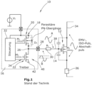
- Fig. 1 shows the situation with regard to the control of an interruption semiconductor switch of an electronic fuse according to the prior art, with no measures being taken to make the control of the electronic fuse regenerative.
- Fig. 1 10 shows a device 10 for controlling an electronic fuse for at least one electrical consumer, in particular in a vehicle.
- the electronic fuse has an interruption semiconductor switch 12, the control electrode 14 of which is controlled by means of a driver 16 with a DC control voltage to close the interruption semiconductor switch 12.
- the driver 16 has a PMOS transistor 18 as a high-side switch 20 and an NMOS transistor 22 as a low-side switch 24.
- the connection node 26 of both switches forms the output connection 28 of the driver 16, which is connected to the control electrode 14 of the interrupting semiconductor switch 12 via a resistor 30 that serves to limit the current.
- the two high-side and low-side switches 20, 24 are controlled by a control unit 32, which in turn receives external signals in order to convert the interruption semiconductor switch into the OFF state if necessary and thus in a targeted manner.
- an interference pulse occurs in the supply line 34, which leads to the electrical consumer indicated at 36, which is caused, for example, by EMC coupling, by an automotive interference pulse according to ISO7637 or also by a pulse as a result of a switching process of the semiconductor switch 12 shown structure or a semiconductor switch in a parallel, similarly constructed circuit arrangement (according to Fig.1 ) can be done. Because of the parasitic capacitive coupling of the control electrode 14 of the interruption semiconductor switch 12 to the other connections of this semiconductor switch, the interference pulses or the interference signal reach the control line 38 between the control electrode 14 and the output connection 28 of the driver 16.
- the driver points 16 has an asymmetrical structure, namely because the high-side switch 20 is a PMOS transistor 18 and the low-side switch 24 is an NMOS transistor 22.
- the driver 16 can also have a differently designed unit 40 (e.g. a resistor or a current source), which is used for the purpose of the intended switching off of the interruption semiconductor switch 12 from its control electrode 14 allows electrical charge to flow to ground 42.
- a differently designed unit 40 e.g. a resistor or a current source
- the electrically effective parasitic diode D 1 between drain D and the n-well of the PMOS transistor 18 now allows a reverse current through the PMOS transistor 18, which leads to a center potential shift at the output terminal 28 of the driver 16 (see the change in interference signal curves A and B).
- the function of the interruption semiconductor switch 12 is unintentionally impaired or even switched off.
- the interruption semiconductor switch 12 can also be designed as a PMOS transistor.
- the interruption semiconductor switch is always shown as an NMOS transistor.
- the structure of the driver 16 can also have transistors of the same type instead of the PMOS and NMOS transistors shown there, in particular NMOS transistors connected in series instead of the PMOS transistor, which are in separate n-wells or in a common n-well are formed, each or the n-well thus insulating the NMOS transistor from the p-doped semiconductor substrate (see Fig. 12 ).
- Various circuits (interference suppression component arrangements SB) of the driver 16 are described or shown below, with which it is possible to reduce or prevent unwanted switching off of the interruption semiconductor switch 12 as a result of the driver 16 being influenced by interference pulses coupled into the control line 38 .
- the resistance R 1 is in Fig. 1 and all exemplary embodiments of the invention described below are optional and limit the return current flow in the control line 38 if an interference signal is coupled into it.
- the resistor 30 can alternatively also be arranged in the driver 16 (e.g. divided on both sides of the connection node 16 or between this and the output connection 28. These alternatives basically apply to all variants of the invention shown and described here.
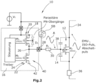
- a capacitance C 1 is connected between the supply voltage V 1 and the output connection 28 of the driver 16, which leads to a reduction in the amplitude of the interference pulse potentially coupled into the control line 38 (see in Fig. 2 at B).
- the capacitance C 1 therefore acts like a filter and in this way reduces the interference level affecting the driver 16 to below the diode voltage of the parasitic diode D 1 . There is therefore no rectifying effect of the interference signal on the control line 38.
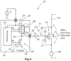
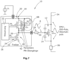
- Fig. 3 is shown how the n-well of the PMOS transistor 18 (high-side switch of the driver 16) can be connected by two diodes D 2 and D 3 connected in anti-parallel, the cathodes of which are connected to each other and to the n-well, in such a way that An increased voltage increase is now permitted at the driver output connection 28 without this having an impact on an inverse switching on of the PMOS transistor.
- the control unit 32 for the PMOS transistor 18 it is possible for the PMOS transistor 18 to be connected to its n-well or to operate it or to be supplied by it.
- This arrangement advantageously provides an implicit discharge to protect against charging of the well of the PMOS transistor 18.
- this optional arrangement serves to avoid a potential shift between the control unit 32 and the control node of the PMOS transistor 18.
- a Schottky diode D 4 prevents feedback between the output connection 28 and the supply potential.
- the cathode of the Schottky diode D 4 is connected to the n-well of the PMOS transistor 18, while its Anode is connected to Source S.
- the voltage swing on the n-well of the PMOS transistor 18 can be adjusted to avoid charging effects at z.
- B. functional operation can be limited by an optionally provided diode D 5 connected in anti-parallel to D 4 .
- D 4 can also be designed as a Zener diode.
- the resistor R 2 can be used to ensure DC potential equalization with the supply voltage V 1 .
- the resistor R 2 acts statically to discharge the n-well of the PMOS transistor 18 and should be dimensioned so that it has essentially no negative effects on the dissipation of interference pulses dynamically. For the dimensioning of the resistance that needs to be taken into account, see the comments above.
- the diode D 4 according to the exemplary embodiment Fig. 4 can be designed as a Zener diode, which has a function comparable to that of the diodes D 4 and D 5 connected in anti-parallel in the exemplary embodiment Fig. 4 realized.
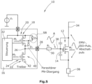
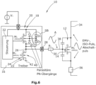
- Fig. 6 An alternative is shown in which the two diodes D 2 and D 3 are connected according to the connection as in Fig. 3 are designed as Schottky diodes.
- a resistor R 2 which represents a DC discharge resistor against the supply to avoid charging effects (keyword: charge pumping). Charging the n-well of the PMOS transistor 18 could result in unwanted threshold voltage increases and, as a result, a reduced performance of the PMOS transistor 18, which can even lead to a lack of switching capability of this transistor. This is prevented by the DC discharge resistor R2 .
- Fig. 8 shows the case that the discharge resistor R 2 is connected between the n-well of the PMOS transistor 18 and its gate G.
- Fig. 9 finally shows the case in which the DC discharge resistor R 2 is connected in parallel to the Schottky diode D 3 .
- an increase in voltage at the output connection 28 of the driver 16 does not have a negative effect on its functioning if interference pulses are coupled in on the control line 38.
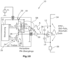
- Fig. 10 The case is shown in which the discharge resistor R 2 is connected between the n-well of the PMOS transistor 18 and ground.
- a simplified well connection of the PMOS transistor 18 via the DC discharge resistor R 2 can be seen. This results in minimal integration effort.
- the diode D 3 is only present as an option, since the well charging can also alternatively take place through the parasitic diode between the drain and the n-well of the PMOS transistor 18.
- Fig. 12 an alternative switch structure to the PMOS transistor 18 of the previous exemplary embodiments is shown.
- the PMOS transistor 18 is replaced by two series-connected NMOS transistors 18a, 18b, each of which is provided with parasitic diodes.
- B 1 denotes a “placeholder” which is intended to alternatively represent one of the arrangements for supplying the well potential of the two NMOS transistors 18a and 18b according to the previous exemplary embodiments.
- the control unit 32 uses the potential located at the n-well of the PMOS transistor 18 for supply.
- This has the advantage that the gate control of the PMOS transistor 18 takes place at a potential that allows the control of the PMOS transistor 18, regardless of the level of potential at the n-well, that is, independent of the level of well charging .
- B 1 denotes a placeholder, which can be one of the previously mentioned alternatives for hanging the tub represented.
- the n-well of the PMOS transistor 18 is coupled (ie electrically connected directly or indirectly) to the gate connection G of the PMOS transistor 18 via an ohmic resistor (not shown).
- Fig. 14 an embodiment in which a diode D 6 is connected between the connection node 26 and drain D of the PMOS transistor 18, which prevents the PMOS transistor 18 from being impaired in terms of its prescribed functionality when interference signals are coupled into the control line 38.
Landscapes
- Electronic Switches (AREA)
- Power Conversion In General (AREA)
- Metal-Oxide And Bipolar Metal-Oxide Semiconductor Integrated Circuits (AREA)
- Fuses (AREA)
Applications Claiming Priority (2)
| Application Number | Priority Date | Filing Date | Title |
|---|---|---|---|
| EP17169691 | 2017-05-05 | ||
| EP18171089.8A EP3419169A3 (fr) | 2017-05-05 | 2018-05-07 | Dispositif de commande d'un fusible électronique pour au moins un consommateur électrique, en particulier d'un véhicule automobile |
Related Parent Applications (1)
| Application Number | Title | Priority Date | Filing Date |
|---|---|---|---|
| EP18171089.8A Division EP3419169A3 (fr) | 2017-05-05 | 2018-05-07 | Dispositif de commande d'un fusible électronique pour au moins un consommateur électrique, en particulier d'un véhicule automobile |
Publications (2)
| Publication Number | Publication Date |
|---|---|
| EP4243286A2 true EP4243286A2 (fr) | 2023-09-13 |
| EP4243286A3 EP4243286A3 (fr) | 2023-10-25 |
Family
ID=58800609
Family Applications (5)
| Application Number | Title | Priority Date | Filing Date |
|---|---|---|---|
| EP18171089.8A Withdrawn EP3419169A3 (fr) | 2017-05-05 | 2018-05-07 | Dispositif de commande d'un fusible électronique pour au moins un consommateur électrique, en particulier d'un véhicule automobile |
| EP23183594.3A Withdrawn EP4239886A3 (fr) | 2017-05-05 | 2018-05-07 | Dispositif de commande d'un fusible électronique pour au moins un consommateur électrique, en particulier d'un véhicule |
| EP23183639.6A Withdrawn EP4239887A3 (fr) | 2017-05-05 | 2018-05-07 | Dispositif de commande d'un fusible électronique pour au moins un consommateur électrique, en particulier d'un véhicule |
| EP23183650.3A Withdrawn EP4239888A3 (fr) | 2017-05-05 | 2018-05-07 | Dispositif de commande d'un fusible électronique pour au moins un consommateur électrique, en particulier d'un véhicule |
| EP23183600.8A Withdrawn EP4243286A3 (fr) | 2017-05-05 | 2018-05-07 | Dispositif de commande d'un fusible électronique pour au moins un consommateur électrique, en particulier d'un véhicule |
Family Applications Before (4)
| Application Number | Title | Priority Date | Filing Date |
|---|---|---|---|
| EP18171089.8A Withdrawn EP3419169A3 (fr) | 2017-05-05 | 2018-05-07 | Dispositif de commande d'un fusible électronique pour au moins un consommateur électrique, en particulier d'un véhicule automobile |
| EP23183594.3A Withdrawn EP4239886A3 (fr) | 2017-05-05 | 2018-05-07 | Dispositif de commande d'un fusible électronique pour au moins un consommateur électrique, en particulier d'un véhicule |
| EP23183639.6A Withdrawn EP4239887A3 (fr) | 2017-05-05 | 2018-05-07 | Dispositif de commande d'un fusible électronique pour au moins un consommateur électrique, en particulier d'un véhicule |
| EP23183650.3A Withdrawn EP4239888A3 (fr) | 2017-05-05 | 2018-05-07 | Dispositif de commande d'un fusible électronique pour au moins un consommateur électrique, en particulier d'un véhicule |
Country Status (1)
| Country | Link |
|---|---|
| EP (5) | EP3419169A3 (fr) |
Family Cites Families (16)
| Publication number | Priority date | Publication date | Assignee | Title |
|---|---|---|---|---|
| US5600525A (en) * | 1994-08-17 | 1997-02-04 | David Sarnoff Research Center Inc | ESD protection circuit for integrated circuit |
| DE69631995T2 (de) * | 1995-06-02 | 2005-02-10 | Siliconix Inc., Santa Clara | Bidirektional sperrender Graben-Leistungs-MOSFET |
| DE19619399A1 (de) * | 1996-05-14 | 1997-11-20 | Telefunken Microelectron | Schaltvorrichtung mit einem Leistungs-FET und einer induktiven Last |
| US5689144A (en) * | 1996-05-15 | 1997-11-18 | Siliconix Incorporated | Four-terminal power MOSFET switch having reduced threshold voltage and on-resistance |
| US6617642B1 (en) * | 2000-02-23 | 2003-09-09 | Tripath Technology, Inc. | Field effect transistor structure for driving inductive loads |
| US6377112B1 (en) * | 2000-12-05 | 2002-04-23 | Semiconductor Components Industries Llc | Circuit and method for PMOS device N-well bias control |
| JP4938307B2 (ja) * | 2005-12-28 | 2012-05-23 | パナソニック株式会社 | スイッチ回路、ダイオード |
| US7626360B2 (en) * | 2006-08-11 | 2009-12-01 | Cirrus Logic, Inc. | Charge-pump biased battery protection circuit |
| US7492212B1 (en) * | 2007-08-21 | 2009-02-17 | Infineon Technologies Ag | Adaptive capacitance for transistor |
| US20090153226A1 (en) * | 2007-10-16 | 2009-06-18 | Texas Instruments Deutschland Gmbh | High-side driver for providing an off-state in case of ground loss |
| US20120091985A1 (en) * | 2010-10-14 | 2012-04-19 | Pieter Gustaaf Nierop | High Voltage Output Driver |
| KR101540147B1 (ko) * | 2012-10-31 | 2015-07-28 | 삼성전기주식회사 | 오작동 방지 기능이 구비된 전력 모듈 및 그 제어 방법 |
| US9214932B2 (en) * | 2013-02-11 | 2015-12-15 | Triquint Semiconductor, Inc. | Body-biased switching device |
| TWI484710B (zh) * | 2013-03-19 | 2015-05-11 | Delta Electronics Inc | 電子保險絲裝置及其操作方法 |
| JP6233270B2 (ja) * | 2014-10-21 | 2017-11-22 | 株式会社デンソー | 保護回路 |
| US9419118B1 (en) * | 2015-11-03 | 2016-08-16 | Ixys Corporation | Trench IGBT with tub-shaped floating P-well and hole drains to P-body regions |
-
2018
- 2018-05-07 EP EP18171089.8A patent/EP3419169A3/fr not_active Withdrawn
- 2018-05-07 EP EP23183594.3A patent/EP4239886A3/fr not_active Withdrawn
- 2018-05-07 EP EP23183639.6A patent/EP4239887A3/fr not_active Withdrawn
- 2018-05-07 EP EP23183650.3A patent/EP4239888A3/fr not_active Withdrawn
- 2018-05-07 EP EP23183600.8A patent/EP4243286A3/fr not_active Withdrawn
Also Published As
| Publication number | Publication date |
|---|---|
| EP4239887A2 (fr) | 2023-09-06 |
| EP3419169A2 (fr) | 2018-12-26 |
| EP4239888A2 (fr) | 2023-09-06 |
| EP4239886A3 (fr) | 2023-10-18 |
| EP4239888A3 (fr) | 2023-10-25 |
| EP3419169A3 (fr) | 2019-05-15 |
| EP4239886A2 (fr) | 2023-09-06 |
| EP4243286A3 (fr) | 2023-10-25 |
| EP4239887A3 (fr) | 2023-10-25 |
Similar Documents
| Publication | Publication Date | Title |
|---|---|---|
| DE102014113636B4 (de) | On-Chip-Verpolungsschutz in Übereinstimmung mit ISO- und ESD-Anforderungen | |
| DE102013218670B4 (de) | Verpolungsschutz für High-Side-Schalter in n-Substrat | |
| DE10046668B4 (de) | Elektrische Lastansteuerungsschaltung mit Schutzeinrichtung | |
| DE19605628C1 (de) | Schaltung zum Vermeiden elektrostatischer Entladung und Latch-up | |
| DE102015102878B4 (de) | Elektronische Ansteuerschaltung | |
| DE102005013687B3 (de) | ESD-Schutzschaltung für niedrige Spannungen | |
| DE102014108576B4 (de) | Treiberschaltung mit Miller-Clamping-Funktionalität für Leistungshalbleiterschalter, Leistungshalbleiterschalter und Wechselrichterbrücke | |
| DE112019004623T5 (de) | Elektronische schaltung und sensorsystem | |
| DE102007044047B4 (de) | Schaltungsanordnung mit einem elektronischen Bauelement und einer ESD-Schutzanordnung | |
| DE112016005269T5 (de) | Umschaltschaltung und Stromversorgungssystem | |
| WO2009030639A1 (fr) | Circuiterie de protection contre les décharges électrostatiques et procédé de déviation de celles-ci | |
| DE102017125802A1 (de) | Elektronikschaltkreis, integrierter Schaltkreis und Motoranordnung | |
| DE10223950B4 (de) | MOS-Leistungstransistor | |
| DE102007053089B4 (de) | Elektrisches und elektronisches System | |
| DE102004062205B4 (de) | Schaltungsanordnung zum Schutz einer Schaltung vor elektrostatischen Entladungen | |
| DE102015122109B4 (de) | Spannungsfester Schalter | |
| DE10255130B4 (de) | Schaltungsanordnung zum Schutz integrierter Schaltungen vor elektrostatischen Entladungen mit parallelem Strompfad | |
| DE102009007818A1 (de) | Schaltungsanordnung mit einer Schaltbrücke aus NMOS-Transistoren und mit einer Verpolschutzeinrichtung | |
| DE10216080B4 (de) | Halbleiter-Bauelement mit Niederimpedanzbereich zum Verpolungsschutz | |
| DE102007018237A1 (de) | Schaltung mit verbessertem ESD-Schutz bei repetierender Pulsbelastung | |
| EP4243286A2 (fr) | Dispositif de commande d'un fusible électronique pour au moins un consommateur électrique, en particulier d'un véhicule | |
| DE102004055057A1 (de) | Ausgangsschaltung | |
| DE19938403C2 (de) | Schaltung | |
| DE10349629B4 (de) | Elektronischer Schaltkreis | |
| DE102006008284B3 (de) | Schaltung mit einer Anordnung zur Detektion einer unterbrochenen Anschlussleitung |
Legal Events
| Date | Code | Title | Description |
|---|---|---|---|
| PUAI | Public reference made under article 153(3) epc to a published international application that has entered the european phase |
Free format text: ORIGINAL CODE: 0009012 |
|
| STAA | Information on the status of an ep patent application or granted ep patent |
Free format text: STATUS: THE APPLICATION HAS BEEN PUBLISHED |
|
| AC | Divisional application: reference to earlier application |
Ref document number: 3419169 Country of ref document: EP Kind code of ref document: P |
|
| AK | Designated contracting states |
Kind code of ref document: A2 Designated state(s): AL AT BE BG CH CY CZ DE DK EE ES FI FR GB GR HR HU IE IS IT LI LT LU LV MC MK MT NL NO PL PT RO RS SE SI SK SM TR |
|
| PUAL | Search report despatched |
Free format text: ORIGINAL CODE: 0009013 |
|
| AK | Designated contracting states |
Kind code of ref document: A3 Designated state(s): AL AT BE BG CH CY CZ DE DK EE ES FI FR GB GR HR HU IE IS IT LI LT LU LV MC MK MT NL NO PL PT RO RS SE SI SK SM TR |
|
| RIC1 | Information provided on ipc code assigned before grant |
Ipc: H03K 17/0412 20060101ALI20230915BHEP Ipc: H01L 27/07 20060101ALI20230915BHEP Ipc: H02H 9/00 20060101ALI20230915BHEP Ipc: H01L 27/092 20060101ALI20230915BHEP Ipc: H02H 3/087 20060101ALI20230915BHEP Ipc: H02M 1/32 20070101ALI20230915BHEP Ipc: H02M 1/08 20060101ALI20230915BHEP Ipc: H03K 17/16 20060101ALI20230915BHEP Ipc: H03K 17/06 20060101AFI20230915BHEP |
|
| STAA | Information on the status of an ep patent application or granted ep patent |
Free format text: STATUS: REQUEST FOR EXAMINATION WAS MADE |
|
| 17P | Request for examination filed |
Effective date: 20240412 |
|
| RBV | Designated contracting states (corrected) |
Designated state(s): AL AT BE BG CH CY CZ DE DK EE ES FI FR GB GR HR HU IE IS IT LI LT LU LV MC MK MT NL NO PL PT RO RS SE SI SK SM TR |
|
| STAA | Information on the status of an ep patent application or granted ep patent |
Free format text: STATUS: EXAMINATION IS IN PROGRESS |
|
| 17Q | First examination report despatched |
Effective date: 20250318 |
|
| STAA | Information on the status of an ep patent application or granted ep patent |
Free format text: STATUS: THE APPLICATION HAS BEEN WITHDRAWN |
|
| 18W | Application withdrawn |
Effective date: 20250721 |