EP4243097A2 - Light-emitting module and display device - Google Patents
Light-emitting module and display device Download PDFInfo
- Publication number
- EP4243097A2 EP4243097A2 EP23179558.4A EP23179558A EP4243097A2 EP 4243097 A2 EP4243097 A2 EP 4243097A2 EP 23179558 A EP23179558 A EP 23179558A EP 4243097 A2 EP4243097 A2 EP 4243097A2
- Authority
- EP
- European Patent Office
- Prior art keywords
- light
- positioning
- emitting
- positioning mark
- substrate
- Prior art date
- Legal status (The legal status is an assumption and is not a legal conclusion. Google has not performed a legal analysis and makes no representation as to the accuracy of the status listed.)
- Granted
Links
Images





Classifications
-
- H—ELECTRICITY
- H10—SEMICONDUCTOR DEVICES; ELECTRIC SOLID-STATE DEVICES NOT OTHERWISE PROVIDED FOR
- H10H—INORGANIC LIGHT-EMITTING SEMICONDUCTOR DEVICES HAVING POTENTIAL BARRIERS
- H10H29/00—Integrated devices, or assemblies of multiple devices, comprising at least one light-emitting semiconductor element covered by group H10H20/00
- H10H29/80—Constructional details
- H10H29/85—Packages
- H10H29/8508—Package substrates, e.g. submounts
-
- H—ELECTRICITY
- H10—SEMICONDUCTOR DEVICES; ELECTRIC SOLID-STATE DEVICES NOT OTHERWISE PROVIDED FOR
- H10W—GENERIC PACKAGES, INTERCONNECTIONS, CONNECTORS OR OTHER CONSTRUCTIONAL DETAILS OF DEVICES COVERED BY CLASS H10
- H10W90/00—Package configurations
-
- H—ELECTRICITY
- H05—ELECTRIC TECHNIQUES NOT OTHERWISE PROVIDED FOR
- H05K—PRINTED CIRCUITS; CASINGS OR CONSTRUCTIONAL DETAILS OF ELECTRIC APPARATUS; MANUFACTURE OF ASSEMBLAGES OF ELECTRICAL COMPONENTS
- H05K1/00—Printed circuits
- H05K1/02—Details
- H05K1/0266—Marks, test patterns or identification means
- H05K1/0269—Marks, test patterns or identification means for visual or optical inspection
-
- H—ELECTRICITY
- H05—ELECTRIC TECHNIQUES NOT OTHERWISE PROVIDED FOR
- H05K—PRINTED CIRCUITS; CASINGS OR CONSTRUCTIONAL DETAILS OF ELECTRIC APPARATUS; MANUFACTURE OF ASSEMBLAGES OF ELECTRICAL COMPONENTS
- H05K1/00—Printed circuits
- H05K1/18—Printed circuits structurally associated with non-printed electric components
- H05K1/181—Printed circuits structurally associated with non-printed electric components associated with surface mounted components
-
- H—ELECTRICITY
- H05—ELECTRIC TECHNIQUES NOT OTHERWISE PROVIDED FOR
- H05K—PRINTED CIRCUITS; CASINGS OR CONSTRUCTIONAL DETAILS OF ELECTRIC APPARATUS; MANUFACTURE OF ASSEMBLAGES OF ELECTRICAL COMPONENTS
- H05K5/00—Casings, cabinets or drawers for electric apparatus
- H05K5/30—Side-by-side or stacked arrangements
-
- G—PHYSICS
- G06—COMPUTING OR CALCULATING; COUNTING
- G06F—ELECTRIC DIGITAL DATA PROCESSING
- G06F3/00—Input arrangements for transferring data to be processed into a form capable of being handled by the computer; Output arrangements for transferring data from processing unit to output unit, e.g. interface arrangements
- G06F3/14—Digital output to display device ; Cooperation and interconnection of the display device with other functional units
- G06F3/1423—Digital output to display device ; Cooperation and interconnection of the display device with other functional units controlling a plurality of local displays, e.g. CRT and flat panel display
- G06F3/1446—Digital output to display device ; Cooperation and interconnection of the display device with other functional units controlling a plurality of local displays, e.g. CRT and flat panel display display composed of modules, e.g. video walls
-
- H—ELECTRICITY
- H05—ELECTRIC TECHNIQUES NOT OTHERWISE PROVIDED FOR
- H05K—PRINTED CIRCUITS; CASINGS OR CONSTRUCTIONAL DETAILS OF ELECTRIC APPARATUS; MANUFACTURE OF ASSEMBLAGES OF ELECTRICAL COMPONENTS
- H05K2201/00—Indexing scheme relating to printed circuits covered by H05K1/00
- H05K2201/10—Details of components or other objects attached to or integrated in a printed circuit board
- H05K2201/10007—Types of components
- H05K2201/10106—Light emitting diode [LED]
-
- H—ELECTRICITY
- H10—SEMICONDUCTOR DEVICES; ELECTRIC SOLID-STATE DEVICES NOT OTHERWISE PROVIDED FOR
- H10H—INORGANIC LIGHT-EMITTING SEMICONDUCTOR DEVICES HAVING POTENTIAL BARRIERS
- H10H29/00—Integrated devices, or assemblies of multiple devices, comprising at least one light-emitting semiconductor element covered by group H10H20/00
- H10H29/01—Manufacture or treatment
- H10H29/036—Manufacture or treatment of packages
Definitions
- the disclosure relates in general to light-emitting modules, and in particular to a light-emitting module with positioning marks.
- display devices are used widely in many aspects of daily life, such as in televisions, computers, notebook computers, cell phones, smartphones, and other modem information devices.
- application of large-sized display devices is becoming more and more popular nowadays.
- multiple light boards, where light-emitting elements are disposed are combined (tiled) and disposed in the cabinet of the display device, serving as a large-sized display device.
- a seam may be visible at the border between two adjacent tiles, and the two adjacent tiles may be not aligned, affecting the appearance of the display device. It is an object of the present invention to overcome the abovementioned disadvantages.
- the light-emitting module includes a light-emitting structure and a carrying substrate.
- the light-emitting structure includes a substrate, a plurality of light-emitting elements, a circuit board, and a hole.
- the carrying substrate includes a protrusion.
- the material of the carrying substrate includes a metallic material.
- the light-emitting structure is disposed on the carrying substrate along a direction, and the hole and the protrusion overlap in the direction.
- the object is further solved by a tiled display device according to claim 5.
- the display device includes a light-emitting module, which includes a light-emitting structure and a carrying substrate.
- the light-emitting structure includes a substrate, a plurality of light-emitting elements, a circuit board, and a hole.
- the carrying substrate includes a protrusion.
- the material of the carrying substrate includes a metallic material.
- the light-emitting structure is disposed on the carrying substrate along a direction, and the hole and the protrusion overlap in the direction.
- first material layer disposed on/over a second material layer may indicate the direct contact of the first material layer and the second material layer, or it may indicate a non-contact state with one or more intermediate layers between the first material layer and the second material layer. In the above situation, the first material layer may not be in direct contact with the second material layer.
- the terms “about”, “substantially” and “approximately” typically mean +/-20% of the stated value, more typically +/- 10% of the stated value, more typically +/-5% of the stated value, more typically +/- 3% of the stated value, more typically +/- 2% of the stated value, more typically +/- 1% of the stated value and even more typically +/-0.5% of the stated value.
- the stated value of the present disclosure is an approximate value. When there is no specific description, the stated value includes the meaning of "about”, “substantially”, or “approximately”.
- overlap in the present disclosure can mean partially overlap or completely overlap.
- first, second, third etc. may be used herein to describe various elements, components, regions, layers and/or portions, and these elements, components, regions, layers, and/or portions should not be limited by these terms. These terms are merely used to distinguish one element, component, region, layer, or portion. Thus, a first element, component, region, layer or portion discussed below could be termed a second element, component, region, layer or portion without departing from the teachings of some embodiments of the present disclosure.
- relative terms such as “downwards,” “upwards,” “horizontal,” “vertical,”, “below,” “above,” “top” and “bottom” as well as derivative thereof (e.g., “horizontally,” “downwardly,” “upwardly,” etc.) should be construed to refer to the orientation as then described or as shown in the drawing under discussion. These relative terms are for convenience of description and do not require that the apparatus be constructed or operated in a particular orientation.
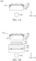
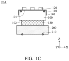
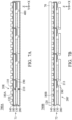
- Figs. 1A-1C are cross-sectional views illustrating the assembly process of a light-emitting module 20A in accordance with some embodiments of the present disclosure.
- the light-emitting module 20A includes a light-emitting structure 10A, a carrying substrate 200, and a bonding layer 130 bonding the light-emitting structure 10A and the carrying substrate 200.
- the carrying substrate 200 can be disposed below and support the light-emitting structure 10A.
- the light-emitting structure 10A includes a substrate 100, a plurality of light-emitting elements 120, and a circuit board 140.
- the substrate 100 may include a transparent substrate, such as a glass substrate, a ceramic substrate, a plastic substrate, or any other suitable substrate, but the substrate 100 is not limited thereto.
- the circuit board 140 is disposed on the substrate 100, wherein the circuit board 140 includes an insulating layer and metal lines (not shown) formed in the insulating layer.
- the circuit board 140 may be a printed circuit board, and the material of the insulating layer may be polyimide (PI) or any other suitable low-k insulating material, but the circuit board 140 is not limited thereto.
- the light-emitting elements 120 are disposed on the substrate 100, wherein the circuit board 140 is disposed between the light-emitting elements 120 and the substrate 100.
- At least one of the light-emitting elements 120 is electrically connected to the circuit board 140.
- the light-emitting elements 120 are electrically connected to an external control unit (not shown) via the circuit board 140.
- the external control unit can transmit electrical signals to the light-emitting elements 120 to control the brightness of the light-emitting elements 120. It should be noted that although three light-emitting elements 120 are illustrated in the present embodiment, the number of light-emitting elements 120 is not limited thereto, and may be adjusted according to practical demand.
- the light-emitting structure 10A includes a first positioning mark 110, and the carrying substrate 200 includes a second positioning mark 210 for subsequent positioning.
- the first positioning mark 110 may be disposed on the substrate 100.
- the first positioning mark 110 may be disposed in the substrate 100.
- the first positioning mark 110 may be disposed on the circuit board 140.
- the first positioning mark 110 may be disposed in the circuit board 140.
- an image of the light-emitting structure 10A can be taken from below by a camera device 300 to capture an image of the first positioning mark 110 and to record the position in a horizontal plane (the X-Y plane).
- the first positioning mark 110 may be metal, color photoresist, a semiconductor layer, etc., but the first positioning marks 110 are not limited thereto.
- the second positioning mark 210 may be metal, color photoresist, a semiconductor layer, etc., but are not limited thereto.
- the assembly and positioning of the light-emitting module 20A are performed based on the position of the first positioning mark 110.
- first positioning marks 110 and two second positioning marks 210 Although the present embodiment is illustrated as having two first positioning marks 110 and two second positioning marks 210, the number of first positioning marks 110 and the number of second positioning marks 210 are not limited thereto, and may be adjusted according to practical demand. In some embodiments, a plurality of the first positioning marks and a plurality of the second positioning marks can be disposed.
- the carrying substrate 200 is provided and disposed on a movable carrying platform 220.
- the material of the carrying substrate 200 can be metallic material (such as aluminum), glass, or plastic material (such as polyethylene terephthalate (PET)), it is not limited thereto.
- PET polyethylene terephthalate
- two second positioning marks 210 are disposed on the carrying substrate 200. An image of the carrying substrate 200 is captured, and the positions of the second positioning marks 210 are recorded.
- the carrying platform 220 is moved along the horizontal plane (the X-Y plane) according to the positions of the second positioning marks 210, making the images of the first positioning marks 110 and the second positioning marks 210 overlap along a vertical direction (the Z-axis direction). That is, in a top view, the first positioning marks 110 and the second positioning marks 210 overlap. Therefore, the alignment of the light-emitting structure 10A with the carrying substrate 200 is completed, and the light-emitting structure 10A is fixed on the carrying substrate 200 along the vertical direction. Regarding the method for determining whether the first positioning marks and the second positioning marks overlap, it will be discussed in further detail in connection with Figs. 3A-3E .
- the bonding layer 130 may be disposed on the carrying substrate 200 for bonding the light-emitting structure 10A to the carrying substrate 200, wherein the bonding layer 130 is an adhesive or any other sticky material, but the bonding layer 130 is not limited thereto.
- the substrate 100 has a first surface 101 and a second surface 102, and the plurality of light-emitting elements 120 are disposed on the first surface 101.
- the light-emitting structure 10A is disposed on the bonding layer 130 such that the light-emitting structure 10A is combined onto the carrying substrate 200, and the assembly of the light-emitting module 20A is complete.
- the bonding layer 130 is adhered between the second surface 102 and the carrying substrate 200.
- the first positioning mark can comprise a hole, a penetrating hole, a blind hole, a protrusion, a concave part, a pattern, a screw, a screw hole, or combinations thereof, and can be disposed on or in the substrate 100.
- the second positioning mark can comprise a hole, a penetrating hole, a blind hole, a protrusion, a concave part, a pattern, a screw, a screw hole, or combinations thereof, and can be disposed on or in the carrying substrate 200.
- the camera device 300 is utilized in the aforementioned manner to aid in the alignment of the light-emitting structure 10A with the carrying substrate 200.
- Fig. 2A is a cross-sectional view illustrating the assembly process of the light-emitting module in accordance with some embodiments of the present disclosure.
- the light-emitting module 20B in the present embodiment may include the same or similar portions as the light-emitting module 20A shown in Figs. 1A-1C . Those portions that are the same or similar will be labeled with similar numerals, and will not be discussed in detail again.
- the difference between the light-emitting module 20B in the present embodiment and the light-emitting module 20A shown in Figs. 1A-1C is that second holes 211 are formed in and penetrate the carrying substrate 200.
- the second holes 211 may serve as the second positioning marks 210A.
- the camera device 300 may capture the image of the first positioning marks 110 through the second holes 211, and record the positions of the first positioning marks 110 in the horizontal plane (the X-Y plane).
- the first positioning mark 110 and the second hole 211 overlap in the vertical direction (the Z-axis direction)
- the light-emitting structure 10A is disposed on the bonding layer 130 such that the light-emitting structure 10A is fixed on the carrying substrate 200.
- the positioning and the assembly of the light-emitting structure 10A and the carrying substrate 200 may be completed in a single step, saving time or related cost in the process.
- the second holes 211 may be provided for the passage of signal lines (not shown), which are configured to transmit electrical signals to the light-emitting elements 120.
- the shape of the second holes 211 may be, for example, circle, oval, triangle, rectangle, hexagon, polygon, irregular shape, or any shape.
- a shape of the first positioning mark 110 may be substantially the same as or similar to a shape of the second positioning mark 211. It is beneficial to determine whether the first positioning mark 110 and the second positioning mark (for example, the second hole 211) overlap or not. Regarding the method for determining whether the first positioning mark and the second positioning mark overlap, it will be discussed in further detail in connection with Figs. 3A-3E .
- Figs. 3A-3E are plan views illustrating the alignment of the first positioning mark with the second positioning mark.
- the first positioning mark and the second positioning mark described in the present embodiment may include any kind of positioning structure mentioned in the embodiments of the present disclosure.
- the first positioning mark and the second positioning mark are viewed from the vertical direction (the Z-axis direction), that is, viewed from a top view.
- the term "area" mentioned in reference with Figs. 3A-3E means the areas of the positioning marks in the horizontal plane (the X-Y plane), which are viewed via the camera device 300.
- a first positioning mark 110A and a second positioning mark 210A are disposed, and both of the first positioning mark 110A and the second positioning mark 210A are circular, wherein the size of the first positioning mark 110A is greater than the size of the second positioning mark 210A.
- the size of the first positioning mark 110A may be substantially equal to or smaller than the size of the second positioning mark 210A.
- a first positioning mark 110B and a second positioning mark 210B are also disposed, and both of the positioning marks are criss-cross patterns.
- the size of the first positioning mark 110B may be greater than, substantially equal to, or smaller than the size of the second positioning mark 210B.
- first positioning marks and/or second positioning marks may also be disposed.
- two first positioning marks 110C and two second positioning marks 210C are disposed, and the area of the first positioning marks 110C is greater than the area of the second positioning marks 210C, wherein the first positioning marks 110C are circular, and the second positioning marks 210C are circular segments.
- the value of the overlapping area of the first positioning mark 110C and the second positioning mark 210C may be greater than or equal to the value of the area of the first positioning mark 110C divided by the number of first positioning marks 110C.
- two first positioning marks 110C are disposed, and the area of the second positioning mark 210C may be greater than or equal to half of the area of the first positioning mark 110C.
- first positioning marks 110D and two second positioning marks 210D are disposed, wherein the size of the second positioning marks 210D is smaller than the size of the first positioning marks 110D.
- Each of the first positioning marks 110D includes two first positioning edges 110D1 and 110D2, and each of the second positioning marks 210D includes two second positioning edges 210D1 and 210D2.
- the first positioning marks 110D and the second positioning marks 210D are positioned by aligning the second positioning edges 210D1 and 210D2 of the second positioning marks 210D with the respective first positioning edges 110D1 and 110D2 of the first positioning marks 110D.
- an irregular polygonal first positioning mark 110E and three second positioning marks 210E with different shapes are disposed, and the positions of the second positioning marks 210E are located in the region of the first positioning mark 110E.
- the second positioning marks 210E and the first positioning mark 110E are positioned by aligning the second positioning edge 210E1 of one of the second positioning marks 210E with the first positioning edge 110E1 of the first positioning mark 110E.
- the number of first positioning edges may be greater than or equal to the total number of edges of the first positioning mark divided by the number of first positioning edges used for positioning.
- the first positioning mark 110D is a rectangle with four edges, and two first positioning marks 110D are disposed in the present embodiment, therefore, the first positioning mark 110D may be positioned by at least two edges (namely, the first positioning edges 110D1 and 110D2) therein.
- first positioning marks serve as an example to discuss the relationship between the area of positioning marks and the number of positioning edges therein in the foregoing paragraphs.
- the relationship between the positioning marks regarding sizes, positions, etc. may be interchangeably applied to the first positioning marks and the second positioning marks.
- the relationship between the areas of the first positioning marks and the number of positioning edges may be applied to the second positioning marks.
- Figs. 4A-4B are cross-sectional views illustrating the assembly process of the light-emitting module 20C in accordance with some embodiments of the present disclosure.
- the light-emitting module 20C in the present embodiment may include the same or similar portions as the light-emitting module 20A shown in Figs. 1A-1C . Those portions that are the same or similar will be labeled with similar numerals, and will not be discussed in detail again.
- solder pads 150 are disposed on the circuit board 140 for bonding the light-emitting elements 120.
- the solder pads 150 shown in Fig. 4A are only roughly illustrated.
- a solder material 151 (shown in Figs. 5B-5D ) will be formed on the solder pad 150 for making the light-emitting element 120 electrically connected to the circuit board 140 via the solder pad 150.
- the process of forming the solder material 151 it will be discussed in further detail in connection with Figs. 5A-5D . As shown in Fig.
- the size of the solder pad 150 is greater than the size of the light-emitting element 120, such that the light-emitting element 120 may cover a portion of the solder pad 150, and expose another portion 110' of the solder pad 150.
- the exposed portion 110' may serve as a first positioning mark of the light-emitting structure 10C.
- the solder pads 150 may have different heights (namely, the position of the solder pads 150 in Z-axis direction). The solder pads 150 with different heights may serve as the first positioning marks of the light-emitting structure 10C for subsequent positioning with the carrying substrate 200.
- the images and positions of the first positioning mark 110' and the second positioning mark 210 may be captured simultaneously by two camera devices 300.
- the first positioning mark can include the exposed portion 110' of the solder pads 150, which is not covered by the light-emitting elements 120.
- the carrying platform 220 is moved for overlapping the first positioning marks and the second positioning marks in the vertical direction (the Z-axis direction), and thereby the light-emitting structure 10C and the carrying substrate 200 are positioned.
- the light-emitting structure 10C is disposed on the bonding layer 130 such that the light-emitting structure 10C is fixed on the carrying substrate 200, assembled as the light-emitting module 20C.
- Figs. 5A-5D are cross-sectional views illustrating the process of arranging light-emitting elements 120 on the substrate 100.
- a shielding layer 170 is formed on the circuit board 140, and the shielding layer 170 may expose the positions of the solder pads 150 formed in the circuit board 140.
- the shielding layer 170 may be an organic material or an insulating material, but the shielding layer 170 is not limited thereto.
- the solder material 151 is filled into gaps between the shielding layer 170.
- the solder material for example, can include tin (that is the solder material 151 is, for example, an alloy including tin), but the solder material 151 is not limited thereto.
- the arrangement of the solder material 151 may be controlled more precisely, such that the solder material 151 may be disposed flat over the solder pads 150, instead of overflowing out of the region of the solder pads 150.
- the area of the region filled with the solder material 151 may be substantially equal to the area of the solder pads 150.
- the light-emitting elements 120 are disposed on the solder pads 150 (namely, on the region filled with the solder material 151), such that the contacts 121 of the light-emitting elements 120 are directly bonded to the solder material 151.
- the exposed portion 110' uncovered by and exposed by the light-emitting elements 120 on the solder pads 150, and the exposed portion 110' can serve as the first positioning mark for subsequent positioning.
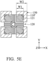
- Fig. 5E is a plan view illustrating the contacts 121 of the light-emitting elements 120 and the solder pads 150. It should be noted that for clearly presenting the dimensional relationship between the solder pads 150 and the light-emitting elements 120, the solder material 151 disposed on the solder pads 150 is not illustrated in the present figure.
- the light-emitting elements 120 include four contacts 121 bonded on four respective solder pads 150. One of the contacts has the first width W1, and the solder pad 150 corresponding to the contact 121 has the second width W2. The rest of the three contacts and the three solder pads may have the same or similar width relationship. The second width W2 may be greater than the first width W1.
- the first width W1 is in a range between about 0.2 mm and about 0.4 mm
- the second width W2 is in a range between about 0.35 mm and about 0.55 mm
- the first width W1 and the second width W2 are not limited thereto.
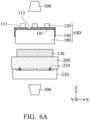
- Figs. 6A-6B are cross-sectional views illustrating the assembly process of the light-emitting module 20D in accordance with some embodiments of the present disclosure.
- the light-emitting module 20D in the present embodiment may include the same or similar portions as the light-emitting module 20A shown in Figs. 1A-1C . Those portions that are the same or similar will be labeled with similar numerals, and will not be discussed in detail again.
- the difference between the light-emitting module 20D in the present embodiment and the light-emitting module 20A shown in Figs. 1A-1C is that in the present embodiment, a first hole 111 may be formed in the light-emitting structure 10D.
- the first hole 111 may be formed in and penetrate the circuit board 140.
- a first hole 112 may be formed in the circuit board 140, but does not penetrate the circuit board 140.
- a special colored region 141 may be formed on the substrate 100 or on the circuit board 140.
- the colored region 141 may have different color, pattern, or text from other portions of the circuit board 140.
- the first holes 111, 112 and/or the colored region 141 may serve as the first positioning marks of the substrate 100, configured to align with the second positioning marks 210 (such as metal marks).
- the first holes 111, 112 and the colored region 141 are illustrated in the present embodiment at the same time, in some other embodiments, one or any two of the first holes 111, 112 and the colored region 141 may also be disposed.
- the image and position of the first positioning mark (such as the first hole 111) and the second positioning mark 210 (such as metal marks) may be captured simultaneously by two camera devices 300.
- the carrying platform 220 is moved such that the first positioning mark and the corresponding second positioning mark can be aligned in the vertical direction (the Z-axis direction), and thereby the light-emitting structure 10D and the carrying substrate 200 are aligned and positioned.
- the light-emitting structure 10D is disposed on the bonding layer 130 such that the light-emitting structure 10D is fixed to the carrying substrate 200 via the bonding layer 130, and the assembly of the light-emitting module 20D is complete.
- Fig. 7A is a cross-sectional view illustrating a display device 700A in accordance with some embodiments of the present disclosure.
- a plurality of light-emitting modules 20E may be disposed in a cabinet 400, combined as the display device 700A.
- the display device 700A may be a tiled display device.
- the light-emitting modules 20E in the present embodiment may include the same or similar portions as the light-emitting module 20A shown in Figs. 1A-1C . Those portions that are the same or similar will be labeled with similar numerals, and will not be discussed in detail again.
- the difference between the light-emitting module 20E in the present embodiment and the light-emitting module 20A shown in Figs. 1A-1C is that a part of the circuit board 140 may extend below the substrate 100 through a sidewall of the substrate 100 to form a lower part, and an electrical component 190 is disposed on the lower part of the circuit board 140.
- At least one of the light-emitting modules 20E may include a light-emitting structure 71 and the carrying substrate 200.
- the light-emitting structure 71 may include a plurality of light-emitting elements 120.
- the light-emitting structure 71 may include a first positioning mark 110, the carrying substrate 200 may include a second positioning mark 210, and the first positioning mark 110 and the second positioning mark 210 may overlap in the vertical direction (Z direction) for positioning, in a manner similar to the above embodiments.
- the electrical component 190 may be an integrated circuit (IC) component, a resistor, an inductor, etc., but the electrical component 190 is not limited thereto. In other embodiments, the electrical component 190 may be any suitable electronic component as required.
- the light-emitting elements 120 may be light-emitting diodes (LED), such as micro-LED or mini-LED. As such, the display device 700A is a tiled LED display device.
- An optical layer such as a light-shielding layer 180A, may be disposed on the circuit board 140 and between the light-emitting elements 120.
- the reflectivity of the light-shielding layer 180A may be between 0% and 10%.
- the material of the light-shielding layer 180A may be photoresist, silicon, organic materials, paint, carbon nanotube, or polymers.
- the polymers may be polycarbonate (PC), polyurethane (PU), polymethyl methacrylate (PMMA), epoxy resin, etc., but the polymers are not limited thereto.
- the light-shielding layer 180A may be any dark or black material with a reflectivity between 0% and 10%, such as black photoresist.
- the display device 700A in Fig. 7A merely shows the first positioning mark 110 and the second positioning mark 210, which are of the same shape or pattern as that in Fig. 1B .
- the first positioning mark and the second positioning mark may also be of other shapes or patterns, and may also be substituted with other types of positioning marks described in the present disclosure, and will not be repeated again.
- Fig. 7B is a cross-sectional view illustrating the display device 700B in accordance with some embodiments of the present disclosure.
- the display device 700B may include a display panel 70 and a light-emitting module 20F.
- the light-emitting module 20F can provide a light source for the display panel 70.
- the light-emitting modules 20F may be backlight modules.
- the present embodiment is illustrated as having four light-emitting modules 20F, a different number of light-emitting modules 20F may be disposed in other embodiments.
- one or more light-emitting modules 20F may provide a light source for the display panel 70.
- the display device 700B can include a plurality of light-emitting modules 20F to provide the light source.
- the display panel 70 for example, may be a liquid-crystal display panel, but the display panel 70 is not limited thereto.
- the light-emitting modules 20F in the present embodiment may include the same or similar portions as the light-emitting modules 20E shown in Fig. 7A . Those portions that are the same or similar will be labeled with similar numerals, and will not be discussed in detail again.
- At least one of the light-emitting modules 20F may include a light-emitting structure 72 and the carrying substrate 200.
- the light-emitting structure 72 may include a plurality of light-emitting elements 120.
- a second hole 211 is formed in the carrying substrate 200, and serves as a second positioning mark.
- the electrical component 190 may serve as a first positioning mark of the light-emitting structure 72.
- the electrical component 190 (the first positioning mark) and the second hole 211 (the second positioning mark) can overlap in the vertical direction, such that the light-emitting structure 72 may be fixed on the carrying substrate 200 along the vertical direction. In other words, as viewed in the vertical direction (the Z-axis direction), the electrical component 190 and the second hole 211 overlap.
- an optical layer may be disposed on the circuit board 140 and between the light-emitting elements 120, such as a light-shielding layer 180A or a reflective layer 180B.
- the electrical component 190 and the second hole 211 which respectively serve as the first positioning mark and the second positioning mark, are shown in the display device 700B of Fig. 7B .
- the first positioning mark and the second positioning mark may also be replaced by other types of positioning marks as described in the present disclosure, and will not be repeated again.
- Fig. 7C is a cross-sectional view illustrating the display device 700C in accordance with some embodiments of the present disclosure.
- a plurality of light-emitting modules 20G may be combined to form the display device 700C.
- the light-emitting modules 20G in the present embodiment may include the same or similar portions as the light-emitting modules 20F shown in Fig. 7B . Those portions that are the same or similar will be labeled with similar numerals, and will not be discussed in detail again.
- At least one of the light-emitting modules 20G may include a light-emitting structure 73 and the carrying substrate 200.
- the light-emitting structure 73 may include a plurality of light-emitting elements 120.
- the difference between the light-emitting modules 20G in the present embodiment and the light-emitting modules 20F shown in Fig. 7B is that the electrical component 190 is disposed in the second holes 211 of the carrying substrate 200. Therefore, the accuracy of positioning may be further enhanced, or the thickness of the bonding layer 130 may be reduced, such that the overall thickness of the display device 700C may be reduced.
- the plurality of light-emitting modules 20G may be disposed in the cabinet and constitute a tiled display device in the manner shown in Fig. 7A .
- the light-emitting modules 20G may be combined with the display panel and constitute a display device in the manner shown in Fig. 7B , which will not be repeated again.
- Fig. 8 is a cross-sectional view illustrating the light-emitting module 20H in accordance with some embodiments of the present disclosure.
- the light-emitting module 20H in the present embodiment may include the same or similar portions as the light-emitting modules 20G shown in Fig. 7C . Those portions that are the same or similar will be labeled with similar numerals, and will not be discussed in detail again.
- the substrate 100 is omitted in the present embodiment, and electrical components 190A, 190B may be disposed on the surface, which faces the carrying substrate 200, of the circuit board 140. That is, the circuit board 140 is in contact with the bonding layer 130.
- the electrical components 190A and 190B may be an integrated circuit (IC) component, resistor, inductor, etc., but the electrical components 190A and 190B are not limited thereto.
- the second hole 211 is formed on the carrying substrate 200, and may penetrate the bonding layer 130 and the carrying substrate 200 simultaneously.
- Another second hole 212 is formed on the carrying substrate 200, the second hole 212 may penetrate the bonding layer 130, but does not penetrate the carrying substrate 200.
- the electrical components 190A, 190B are disposed to align with the second holes 211, 212 (the second positioning marks) respectively, and thereby the effect of precisely positioning is achieved.
- the substrate 100 is omitted in the present embodiment, the circuit board 140 is aligned with the carrying substrate 200, and bonded to the carrying substrate 200 via the bonding layer 130. Since the thickness of the substrate 100 is reduced, the overall thickness of the light-emitting module may also be reduced.
- the above-mentioned light-emitting module can be adjusted such that the substrate 100 can be retained, but the circuit board 140 can be omitted.
- Metal lines (not shown) are disposed on the substrate 100 in these embodiments, and the metal lines are configured to transmit electrical signals to the light-emitting elements 120. Since the substrate 100 generally is made of material with a higher flatness (such as glass, but it is not limited thereto), this will increase the flatness of the light-emitting module, such that the yield of arranging elements on the substrate 100 may also be increased.
- the light-emitting module includes positioning marks.
- positioning procedure can be performed precisely. Therefore, the time or related cost required for the process may be reduced.
- the display devices and the light-emitting modules are not limited to the configurations shown in Figs. 1A-8 . Some embodiments of the present disclosure may just include any one or more features of any one or more embodiments of Figs. 1A-8 . That is to say, according to some other embodiments, there is no need that the display device and the light-emitting module include all the features in the drawings of the above-mentioned embodiments.
Landscapes
- Engineering & Computer Science (AREA)
- Microelectronics & Electronic Packaging (AREA)
- Led Device Packages (AREA)
- Fastening Of Light Sources Or Lamp Holders (AREA)
- Electroluminescent Light Sources (AREA)
- Illuminated Signs And Luminous Advertising (AREA)
Abstract
Description
- The disclosure relates in general to light-emitting modules, and in particular to a light-emitting module with positioning marks.
- As digital technology develops, display devices are used widely in many aspects of daily life, such as in televisions, computers, notebook computers, cell phones, smartphones, and other modem information devices. In addition, the application of large-sized display devices is becoming more and more popular nowadays. Currently, multiple light boards, where light-emitting elements are disposed, are combined (tiled) and disposed in the cabinet of the display device, serving as a large-sized display device. However, a seam may be visible at the border between two adjacent tiles, and the two adjacent tiles may be not aligned, affecting the appearance of the display device. It is an object of the present invention to overcome the abovementioned disadvantages.
- This object is inventively solved by a light-emitting module according to claim 1. The light-emitting module includes a light-emitting structure and a carrying substrate. The light-emitting structure includes a substrate, a plurality of light-emitting elements, a circuit board, and a hole. The carrying substrate includes a protrusion. The material of the carrying substrate includes a metallic material. The light-emitting structure is disposed on the carrying substrate along a direction, and the hole and the protrusion overlap in the direction.
- The object is further solved by a tiled display device according to
claim 5. The display device includes a light-emitting module, which includes a light-emitting structure and a carrying substrate. The light-emitting structure includes a substrate, a plurality of light-emitting elements, a circuit board, and a hole. The carrying substrate includes a protrusion. The material of the carrying substrate includes a metallic material. The light-emitting structure is disposed on the carrying substrate along a direction, and the hole and the protrusion overlap in the direction. - Further advantageous embodiments are the subject of dependent claims.
- To clarify the features and advantages of the present disclosure, a detailed description is given in the following embodiments with reference to the accompanying drawings.
- The disclosure can be more fully understood by reading the subsequent detailed description and examples with references made to the accompanying drawings, wherein:
-
Figs. 1A-1C are cross-sectional views illustrating an assembly process of a light-emitting module in accordance with some embodiments of the present disclosure. -
Figs. 2A-2B are cross-sectional views illustrating the assembly process of the light-emitting module in accordance with some embodiments of the present disclosure. -
Figs. 3A-3E are plan views illustrating the alignment of first positioning marks with second positioning marks. -
Figs. 4A-4B are cross-sectional views illustrating the assembly process of the light-emitting module in accordance with some embodiments of the present disclosure. -
Figs. 5A-5D are cross-sectional views illustrating the course of arranging light-emitting elements on a light-emitting structure. -
Fig. 5E is a plan view illustrating contacts between solder pads and the light-emitting elements. -
Figs. 6A-6B are cross-sectional views illustrating the assembly process of the light-emitting module in accordance with some embodiments of the present disclosure. -
Figs. 7A-7C are cross-sectional views illustrating the display device in accordance with some embodiments of the present disclosure. -
Fig. 8 is a cross-sectional view illustrating the light-emitting module in accordance with some embodiments of the present disclosure. - The display devices and the light-emitting modules therein in accordance with some embodiments are described in detail in the following description. It should be appreciated that in the following detailed description provides various embodiments and examples in order to perform various configurations of some embodiments of the present disclosure. The specific elements and configurations described in the following detailed description are set forth in order to clearly describe some embodiments of the present disclosure. It will be apparent that the exemplary embodiments set forth herein are used merely for the purpose of illustration, and the inventive concept may be embodied in various forms without being limited to those exemplary embodiments. In addition, the drawings of different embodiments may use repeated numerals or marks. Those repetitions are merely in order to clearly describe some embodiments of the present disclosure. However, the use of repeated numerals in the drawings of different embodiments does not suggest any correlation between different embodiments and/or configurations. In addition, in this specification, expressions such as "first material layer disposed on/over a second material layer", may indicate the direct contact of the first material layer and the second material layer, or it may indicate a non-contact state with one or more intermediate layers between the first material layer and the second material layer. In the above situation, the first material layer may not be in direct contact with the second material layer.
- The terms "about", "substantially" and "approximately" typically mean +/-20% of the stated value, more typically +/- 10% of the stated value, more typically +/-5% of the stated value, more typically +/- 3% of the stated value, more typically +/- 2% of the stated value, more typically +/- 1% of the stated value and even more typically +/-0.5% of the stated value. The stated value of the present disclosure is an approximate value. When there is no specific description, the stated value includes the meaning of "about", "substantially", or "approximately". The term "overlap" in the present disclosure can mean partially overlap or completely overlap.
- It should be understood that, although the terms "first", "second", "third" etc. may be used herein to describe various elements, components, regions, layers and/or portions, and these elements, components, regions, layers, and/or portions should not be limited by these terms. These terms are merely used to distinguish one element, component, region, layer, or portion. Thus, a first element, component, region, layer or portion discussed below could be termed a second element, component, region, layer or portion without departing from the teachings of some embodiments of the present disclosure.
- This description of the exemplary embodiments is intended to be read in connection with the accompanying drawings, which are to be considered part of the entire written description. It should be appreciated that the drawings are not drawn to scale. The shape and the thickness of embodiments may be exaggerated in the drawings to clarify the features of the present disclosure. In addition, structures and devices are shown schematically in order to clarify the features of the present disclosure.
- In some embodiments of the present disclosure, relative terms such as "downwards," "upwards," "horizontal," "vertical,", "below," "above," "top" and "bottom" as well as derivative thereof (e.g., "horizontally," "downwardly," "upwardly," etc.) should be construed to refer to the orientation as then described or as shown in the drawing under discussion. These relative terms are for convenience of description and do not require that the apparatus be constructed or operated in a particular orientation.
- First, referring to
Figs. 1A-1C, Figs. 1A-1C are cross-sectional views illustrating the assembly process of a light-emittingmodule 20A in accordance with some embodiments of the present disclosure. The light-emittingmodule 20A includes a light-emittingstructure 10A, a carryingsubstrate 200, and abonding layer 130 bonding the light-emittingstructure 10A and the carryingsubstrate 200. The carryingsubstrate 200 can be disposed below and support the light-emittingstructure 10A. As shown inFig. 1A , the light-emittingstructure 10A includes asubstrate 100, a plurality of light-emittingelements 120, and acircuit board 140. Thesubstrate 100 may include a transparent substrate, such as a glass substrate, a ceramic substrate, a plastic substrate, or any other suitable substrate, but thesubstrate 100 is not limited thereto. In the present embodiment, thecircuit board 140 is disposed on thesubstrate 100, wherein thecircuit board 140 includes an insulating layer and metal lines (not shown) formed in the insulating layer. For example, thecircuit board 140 may be a printed circuit board, and the material of the insulating layer may be polyimide (PI) or any other suitable low-k insulating material, but thecircuit board 140 is not limited thereto. The light-emittingelements 120 are disposed on thesubstrate 100, wherein thecircuit board 140 is disposed between the light-emittingelements 120 and thesubstrate 100. In some embodiments, at least one of the light-emittingelements 120 is electrically connected to thecircuit board 140. In some embodiments, for example, the light-emittingelements 120 are electrically connected to an external control unit (not shown) via thecircuit board 140. The external control unit can transmit electrical signals to the light-emittingelements 120 to control the brightness of the light-emittingelements 120. It should be noted that although three light-emittingelements 120 are illustrated in the present embodiment, the number of light-emittingelements 120 is not limited thereto, and may be adjusted according to practical demand. - For positioning the light-emitting
structure 10A and the carryingsubstrate 200 to perform the assembly, the light-emittingstructure 10A includes afirst positioning mark 110, and the carryingsubstrate 200 includes asecond positioning mark 210 for subsequent positioning. According to some embodiments, thefirst positioning mark 110 may be disposed on thesubstrate 100. Alternatively, according to some embodiments, thefirst positioning mark 110 may be disposed in thesubstrate 100. Alternatively, according to some embodiments, thefirst positioning mark 110 may be disposed on thecircuit board 140. Alternatively, according to some embodiments, thefirst positioning mark 110 may be disposed in thecircuit board 140. - First, referring to
Fig. 1A , an image of the light-emittingstructure 10A can be taken from below by acamera device 300 to capture an image of thefirst positioning mark 110 and to record the position in a horizontal plane (the X-Y plane). Thefirst positioning mark 110 may be metal, color photoresist, a semiconductor layer, etc., but the first positioning marks 110 are not limited thereto. Thesecond positioning mark 210 may be metal, color photoresist, a semiconductor layer, etc., but are not limited thereto. Subsequently, the assembly and positioning of the light-emittingmodule 20A are performed based on the position of thefirst positioning mark 110. Although the present embodiment is illustrated as having two first positioning marks 110 and two second positioning marks 210, the number of first positioning marks 110 and the number of second positioning marks 210 are not limited thereto, and may be adjusted according to practical demand. In some embodiments, a plurality of the first positioning marks and a plurality of the second positioning marks can be disposed. - Next, as shown in
Fig. 1B , the carryingsubstrate 200 is provided and disposed on amovable carrying platform 220. For example, in the present embodiment, the material of the carryingsubstrate 200 can be metallic material (such as aluminum), glass, or plastic material (such as polyethylene terephthalate (PET)), it is not limited thereto. For positioning the carryingsubstrate 200 and the light-emittingstructure 10A to perform the assembly, two second positioning marks 210 are disposed on the carryingsubstrate 200. An image of the carryingsubstrate 200 is captured, and the positions of the second positioning marks 210 are recorded. Then, the carryingplatform 220 is moved along the horizontal plane (the X-Y plane) according to the positions of the second positioning marks 210, making the images of the first positioning marks 110 and the second positioning marks 210 overlap along a vertical direction (the Z-axis direction). That is, in a top view, the first positioning marks 110 and the second positioning marks 210 overlap. Therefore, the alignment of the light-emittingstructure 10A with the carryingsubstrate 200 is completed, and the light-emittingstructure 10A is fixed on the carryingsubstrate 200 along the vertical direction. Regarding the method for determining whether the first positioning marks and the second positioning marks overlap, it will be discussed in further detail in connection withFigs. 3A-3E . In addition, thebonding layer 130 may be disposed on the carryingsubstrate 200 for bonding the light-emittingstructure 10A to the carryingsubstrate 200, wherein thebonding layer 130 is an adhesive or any other sticky material, but thebonding layer 130 is not limited thereto. As shown inFIG. 1B , thesubstrate 100 has afirst surface 101 and asecond surface 102, and the plurality of light-emittingelements 120 are disposed on thefirst surface 101. - As shown in
Fig. 1C , after determining that the first positioning marks 110 and the second positioning marks 210 overlap, the light-emittingstructure 10A is disposed on thebonding layer 130 such that the light-emittingstructure 10A is combined onto the carryingsubstrate 200, and the assembly of the light-emittingmodule 20A is complete. Thebonding layer 130 is adhered between thesecond surface 102 and the carryingsubstrate 200. By arranging the carryingsubstrate 200, the thermal-dissipation or buffer effect of the light-emittingmodule 20A may be enhanced, or the flatness of the light-emittingmodule 20A may be increased. - Furthermore, in some other embodiments, the first positioning mark can comprise a hole, a penetrating hole, a blind hole, a protrusion, a concave part, a pattern, a screw, a screw hole, or combinations thereof, and can be disposed on or in the
substrate 100. Similarly, in some embodiments, the second positioning mark can comprise a hole, a penetrating hole, a blind hole, a protrusion, a concave part, a pattern, a screw, a screw hole, or combinations thereof, and can be disposed on or in the carryingsubstrate 200. Thecamera device 300 is utilized in the aforementioned manner to aid in the alignment of the light-emittingstructure 10A with the carryingsubstrate 200. - Next, referring to
Fig. 2A, Fig. 2A is a cross-sectional view illustrating the assembly process of the light-emitting module in accordance with some embodiments of the present disclosure. It should be noted that the light-emittingmodule 20B in the present embodiment may include the same or similar portions as the light-emittingmodule 20A shown inFigs. 1A-1C . Those portions that are the same or similar will be labeled with similar numerals, and will not be discussed in detail again. The difference between the light-emittingmodule 20B in the present embodiment and the light-emittingmodule 20A shown inFigs. 1A-1C is thatsecond holes 211 are formed in and penetrate the carryingsubstrate 200. Thesecond holes 211 may serve as the second positioning marks 210A. As such, thecamera device 300 may capture the image of the first positioning marks 110 through thesecond holes 211, and record the positions of the first positioning marks 110 in the horizontal plane (the X-Y plane). As shown inFig. 2B , after determining that thefirst positioning mark 110 and the second hole 211 (the second positioning marks 210A) overlap in the vertical direction (the Z-axis direction), the light-emittingstructure 10A is disposed on thebonding layer 130 such that the light-emittingstructure 10A is fixed on the carryingsubstrate 200. By arranging thesecond holes 211, the positioning and the assembly of the light-emittingstructure 10A and the carryingsubstrate 200 may be completed in a single step, saving time or related cost in the process. In addition, in some embodiments, thesecond holes 211 may be provided for the passage of signal lines (not shown), which are configured to transmit electrical signals to the light-emittingelements 120. - It should be noted that in some embodiments, the shape of the
second holes 211 may be, for example, circle, oval, triangle, rectangle, hexagon, polygon, irregular shape, or any shape. According to some embodiments, a shape of thefirst positioning mark 110 may be substantially the same as or similar to a shape of thesecond positioning mark 211. It is beneficial to determine whether thefirst positioning mark 110 and the second positioning mark (for example, the second hole 211) overlap or not. Regarding the method for determining whether the first positioning mark and the second positioning mark overlap, it will be discussed in further detail in connection withFigs. 3A-3E . - Referring to
Figs. 3A-3E, Figs. 3A-3E are plan views illustrating the alignment of the first positioning mark with the second positioning mark. It should be noted that the first positioning mark and the second positioning mark described in the present embodiment may include any kind of positioning structure mentioned in the embodiments of the present disclosure. In addition, inFigs. 3A-3E , the first positioning mark and the second positioning mark are viewed from the vertical direction (the Z-axis direction), that is, viewed from a top view. The term "area" mentioned in reference withFigs. 3A-3E means the areas of the positioning marks in the horizontal plane (the X-Y plane), which are viewed via thecamera device 300. - As shown in
Fig. 3A , in the present embodiment, afirst positioning mark 110A and asecond positioning mark 210A are disposed, and both of thefirst positioning mark 110A and thesecond positioning mark 210A are circular, wherein the size of thefirst positioning mark 110A is greater than the size of thesecond positioning mark 210A. In some other embodiments, the size of thefirst positioning mark 110A may be substantially equal to or smaller than the size of thesecond positioning mark 210A. When the areas of thefirst positioning mark 110A and thesecond positioning mark 210A completely overlap, thefirst positioning mark 110A and thesecond positioning mark 210A may be determined to be aligned, and the subsequent operation for bonding the light-emittingstructure 10A onto the carryingsubstrate 200 may be performed. - As shown in
Fig. 3B , in the present embodiment, afirst positioning mark 110B and asecond positioning mark 210B are also disposed, and both of the positioning marks are criss-cross patterns. Similarly, the size of thefirst positioning mark 110B may be greater than, substantially equal to, or smaller than the size of thesecond positioning mark 210B. When the areas of thefirst positioning mark 110B and thesecond positioning mark 210B completely overlap, thefirst positioning mark 110B and thesecond positioning mark 210B may be determined to be aligned, and the subsequent operation for bonding the light-emittingstructure 10A to the carryingsubstrate 200 may be performed. - In addition, besides the aforementioned embodiments where single first positioning mark and/or second positioning mark is disposed, a plurality of first positioning marks and/or second positioning marks may also be disposed. As shown in
Fig. 3C , in the present embodiment, two first positioning marks 110C and two second positioning marks 210C are disposed, and the area of the first positioning marks 110C is greater than the area of the second positioning marks 210C, wherein the first positioning marks 110C are circular, and the second positioning marks 210C are circular segments. According to some embodiments, the value of the overlapping area of thefirst positioning mark 110C and thesecond positioning mark 210C may be greater than or equal to the value of the area of thefirst positioning mark 110C divided by the number of first positioning marks 110C. For example, as shown inFig. 3C , two first positioning marks 110C are disposed, and the area of thesecond positioning mark 210C may be greater than or equal to half of the area of thefirst positioning mark 110C. - As shown in
Fig. 3D , in the present embodiment, two rectangular first positioning marks 110D and two second positioning marks 210D are disposed, wherein the size of the second positioning marks 210D is smaller than the size of the first positioning marks 110D. Each of the first positioning marks 110D includes two first positioning edges 110D1 and 110D2, and each of the second positioning marks 210D includes two second positioning edges 210D1 and 210D2. The first positioning marks 110D and the second positioning marks 210D are positioned by aligning the second positioning edges 210D1 and 210D2 of the second positioning marks 210D with the respective first positioning edges 110D1 and 110D2 of the first positioning marks 110D. - As shown in
Fig. 3E , in the present embodiment, an irregular polygonalfirst positioning mark 110E and three second positioning marks 210E with different shapes are disposed, and the positions of the second positioning marks 210E are located in the region of thefirst positioning mark 110E. The second positioning marks 210E and thefirst positioning mark 110E are positioned by aligning the second positioning edge 210E1 of one of the second positioning marks 210E with the first positioning edge 110E1 of thefirst positioning mark 110E. - According to some embodiments, the number of first positioning edges may be greater than or equal to the total number of edges of the first positioning mark divided by the number of first positioning edges used for positioning. In terms of the embodiment shown in
Fig. 3D , thefirst positioning mark 110D is a rectangle with four edges, and twofirst positioning marks 110D are disposed in the present embodiment, therefore, thefirst positioning mark 110D may be positioned by at least two edges (namely, the first positioning edges 110D1 and 110D2) therein. - It should be noted that the first positioning marks serve as an example to discuss the relationship between the area of positioning marks and the number of positioning edges therein in the foregoing paragraphs. However, those skilled in the art will realize that in the aforementioned embodiments, the relationship between the positioning marks regarding sizes, positions, etc. may be interchangeably applied to the first positioning marks and the second positioning marks. In other words, the relationship between the areas of the first positioning marks and the number of positioning edges may be applied to the second positioning marks. For the simplicity of the specification, it will not be repeated in the following description again.
- Next, referring to
Figs. 4A-4B, Figs. 4A-4B are cross-sectional views illustrating the assembly process of the light-emittingmodule 20C in accordance with some embodiments of the present disclosure. It should be noted that the light-emittingmodule 20C in the present embodiment may include the same or similar portions as the light-emittingmodule 20A shown inFigs. 1A-1C . Those portions that are the same or similar will be labeled with similar numerals, and will not be discussed in detail again. The difference between the light-emittingmodule 20C in the present embodiment and the light-emittingmodule 20A shown inFigs. 1A-1C is that thesolder pads 150 are disposed on thecircuit board 140 for bonding the light-emittingelements 120. Thesolder pads 150 shown inFig. 4A are only roughly illustrated. A solder material 151 (shown inFigs. 5B-5D ) will be formed on thesolder pad 150 for making the light-emittingelement 120 electrically connected to thecircuit board 140 via thesolder pad 150. Regarding the process of forming thesolder material 151, it will be discussed in further detail in connection withFigs. 5A-5D . As shown inFig. 4A , the size of thesolder pad 150 is greater than the size of the light-emittingelement 120, such that the light-emittingelement 120 may cover a portion of thesolder pad 150, and expose another portion 110' of thesolder pad 150. The exposed portion 110' may serve as a first positioning mark of the light-emittingstructure 10C. In addition, in some other embodiments, thesolder pads 150 may have different heights (namely, the position of thesolder pads 150 in Z-axis direction). Thesolder pads 150 with different heights may serve as the first positioning marks of the light-emittingstructure 10C for subsequent positioning with the carryingsubstrate 200. - As shown in
Fig. 4A , the images and positions of the first positioning mark 110' and thesecond positioning mark 210 may be captured simultaneously by twocamera devices 300. The first positioning mark can include the exposed portion 110' of thesolder pads 150, which is not covered by the light-emittingelements 120. The carryingplatform 220 is moved for overlapping the first positioning marks and the second positioning marks in the vertical direction (the Z-axis direction), and thereby the light-emittingstructure 10C and the carryingsubstrate 200 are positioned. After determining that the exposed portion 110' (the first positioning marks) and the second positioning marks 210 overlap in the vertical direction (the Z-axis direction), the light-emittingstructure 10C is disposed on thebonding layer 130 such that the light-emittingstructure 10C is fixed on the carryingsubstrate 200, assembled as the light-emittingmodule 20C. - Referring to
Figs. 5A-5D, Figs. 5A-5D are cross-sectional views illustrating the process of arranging light-emittingelements 120 on thesubstrate 100. First, as shown inFig. 5A , ashielding layer 170 is formed on thecircuit board 140, and theshielding layer 170 may expose the positions of thesolder pads 150 formed in thecircuit board 140. For example, theshielding layer 170 may be an organic material or an insulating material, but theshielding layer 170 is not limited thereto. Then, thesolder material 151 is filled into gaps between theshielding layer 170. The solder material, for example, can include tin (that is thesolder material 151 is, for example, an alloy including tin), but thesolder material 151 is not limited thereto. By arranging theshielding layer 170, the arrangement of thesolder material 151 may be controlled more precisely, such that thesolder material 151 may be disposed flat over thesolder pads 150, instead of overflowing out of the region of thesolder pads 150. In other words, as viewed in the vertical direction (the Z-axis direction), the area of the region filled with thesolder material 151 may be substantially equal to the area of thesolder pads 150. - After filling the
solder material 151, the light-emittingelements 120 are disposed on the solder pads 150 (namely, on the region filled with the solder material 151), such that thecontacts 121 of the light-emittingelements 120 are directly bonded to thesolder material 151. As shown inFig. 5D , there is the exposed portion 110' uncovered by and exposed by the light-emittingelements 120 on thesolder pads 150, and the exposed portion 110' can serve as the first positioning mark for subsequent positioning. - Referring to
Fig. 5E, Fig. 5E is a plan view illustrating thecontacts 121 of the light-emittingelements 120 and thesolder pads 150. It should be noted that for clearly presenting the dimensional relationship between thesolder pads 150 and the light-emittingelements 120, thesolder material 151 disposed on thesolder pads 150 is not illustrated in the present figure. As shown inFig. 5E , the light-emittingelements 120 include fourcontacts 121 bonded on fourrespective solder pads 150. One of the contacts has the first width W1, and thesolder pad 150 corresponding to thecontact 121 has the second width W2. The rest of the three contacts and the three solder pads may have the same or similar width relationship. The second width W2 may be greater than the first width W1. For example, the first width W1 is in a range between about 0.2 mm and about 0.4 mm, the second width W2 is in a range between about 0.35 mm and about 0.55 mm, but the first width W1 and the second width W2 are not limited thereto. - Referring to
Figs. 6A-6B, Figs. 6A-6B are cross-sectional views illustrating the assembly process of the light-emittingmodule 20D in accordance with some embodiments of the present disclosure. It should be noted that the light-emittingmodule 20D in the present embodiment may include the same or similar portions as the light-emittingmodule 20A shown inFigs. 1A-1C . Those portions that are the same or similar will be labeled with similar numerals, and will not be discussed in detail again. The difference between the light-emittingmodule 20D in the present embodiment and the light-emittingmodule 20A shown inFigs. 1A-1C is that in the present embodiment, afirst hole 111 may be formed in the light-emittingstructure 10D. Specifically, thefirst hole 111 may be formed in and penetrate thecircuit board 140. On the other hand, afirst hole 112 may be formed in thecircuit board 140, but does not penetrate thecircuit board 140. In addition, a specialcolored region 141 may be formed on thesubstrate 100 or on thecircuit board 140. Thecolored region 141 may have different color, pattern, or text from other portions of thecircuit board 140. Thefirst holes colored region 141 may serve as the first positioning marks of thesubstrate 100, configured to align with the second positioning marks 210 (such as metal marks). Although thefirst holes colored region 141 are illustrated in the present embodiment at the same time, in some other embodiments, one or any two of thefirst holes colored region 141 may also be disposed. - As shown in
Figs. 6A-6B , the image and position of the first positioning mark (such as the first hole 111) and the second positioning mark 210 (such as metal marks) may be captured simultaneously by twocamera devices 300. The carryingplatform 220 is moved such that the first positioning mark and the corresponding second positioning mark can be aligned in the vertical direction (the Z-axis direction), and thereby the light-emittingstructure 10D and the carryingsubstrate 200 are aligned and positioned. After determining that the first positioning mark (such as the first holes 111) and the second positioning mark 210 (such as metal mark) overlap in the vertical direction (the Z-axis direction), the light-emittingstructure 10D is disposed on thebonding layer 130 such that the light-emittingstructure 10D is fixed to the carryingsubstrate 200 via thebonding layer 130, and the assembly of the light-emittingmodule 20D is complete. - Referring to
Fig. 7A, Fig. 7A is a cross-sectional view illustrating adisplay device 700A in accordance with some embodiments of the present disclosure. As shown inFig. 7A , a plurality of light-emittingmodules 20E may be disposed in acabinet 400, combined as thedisplay device 700A. Thedisplay device 700A may be a tiled display device. It should be noted that the light-emittingmodules 20E in the present embodiment may include the same or similar portions as the light-emittingmodule 20A shown inFigs. 1A-1C . Those portions that are the same or similar will be labeled with similar numerals, and will not be discussed in detail again. The difference between the light-emittingmodule 20E in the present embodiment and the light-emittingmodule 20A shown inFigs. 1A-1C is that a part of thecircuit board 140 may extend below thesubstrate 100 through a sidewall of thesubstrate 100 to form a lower part, and anelectrical component 190 is disposed on the lower part of thecircuit board 140. At least one of the light-emittingmodules 20E may include a light-emitting structure 71 and the carryingsubstrate 200. The light-emitting structure 71 may include a plurality of light-emittingelements 120. Similarly to the aforementioned embodiments, the light-emitting structure 71 may include afirst positioning mark 110, the carryingsubstrate 200 may include asecond positioning mark 210, and thefirst positioning mark 110 and thesecond positioning mark 210 may overlap in the vertical direction (Z direction) for positioning, in a manner similar to the above embodiments. Theelectrical component 190 may be an integrated circuit (IC) component, a resistor, an inductor, etc., but theelectrical component 190 is not limited thereto. In other embodiments, theelectrical component 190 may be any suitable electronic component as required. The light-emittingelements 120 may be light-emitting diodes (LED), such as micro-LED or mini-LED. As such, thedisplay device 700A is a tiled LED display device. - An optical layer, such as a light-
shielding layer 180A, may be disposed on thecircuit board 140 and between the light-emittingelements 120. The reflectivity of the light-shielding layer 180A may be between 0% and 10%. For example, the material of the light-shielding layer 180A may be photoresist, silicon, organic materials, paint, carbon nanotube, or polymers. Examples for the polymers may be polycarbonate (PC), polyurethane (PU), polymethyl methacrylate (PMMA), epoxy resin, etc., but the polymers are not limited thereto. In some other embodiments, the light-shielding layer 180A may be any dark or black material with a reflectivity between 0% and 10%, such as black photoresist. - For the sake of the convenience of description, the
display device 700A inFig. 7A merely shows thefirst positioning mark 110 and thesecond positioning mark 210, which are of the same shape or pattern as that inFig. 1B . However, according to other embodiments, the first positioning mark and the second positioning mark may also be of other shapes or patterns, and may also be substituted with other types of positioning marks described in the present disclosure, and will not be repeated again. - Referring to
Fig. 7B, Fig. 7B is a cross-sectional view illustrating thedisplay device 700B in accordance with some embodiments of the present disclosure. As shown inFig. 7B , thedisplay device 700B may include adisplay panel 70 and a light-emittingmodule 20F. The light-emittingmodule 20F can provide a light source for thedisplay panel 70. The light-emittingmodules 20F may be backlight modules. Although the present embodiment is illustrated as having four light-emittingmodules 20F, a different number of light-emittingmodules 20F may be disposed in other embodiments. For example, one or more light-emittingmodules 20F may provide a light source for thedisplay panel 70. Thedisplay device 700B can include a plurality of light-emittingmodules 20F to provide the light source. Thedisplay panel 70, for example, may be a liquid-crystal display panel, but thedisplay panel 70 is not limited thereto. It should be noted that the light-emittingmodules 20F in the present embodiment may include the same or similar portions as the light-emittingmodules 20E shown inFig. 7A . Those portions that are the same or similar will be labeled with similar numerals, and will not be discussed in detail again. At least one of the light-emittingmodules 20F may include a light-emittingstructure 72 and the carryingsubstrate 200. The light-emittingstructure 72 may include a plurality of light-emittingelements 120. The difference between the light-emittingmodules 20F in the present embodiment and the light-emittingmodules 20E shown inFig. 7A is that different types of the first positioning marks and the second positioning marks may be utilized. Asecond hole 211 is formed in the carryingsubstrate 200, and serves as a second positioning mark. Theelectrical component 190 may serve as a first positioning mark of the light-emittingstructure 72. The electrical component 190 (the first positioning mark) and the second hole 211 (the second positioning mark) can overlap in the vertical direction, such that the light-emittingstructure 72 may be fixed on the carryingsubstrate 200 along the vertical direction. In other words, as viewed in the vertical direction (the Z-axis direction), theelectrical component 190 and thesecond hole 211 overlap. In addition, an optical layer may be disposed on thecircuit board 140 and between the light-emittingelements 120, such as a light-shielding layer 180A or areflective layer 180B. - For the sake of the convenience of description, the
electrical component 190 and thesecond hole 211, which respectively serve as the first positioning mark and the second positioning mark, are shown in thedisplay device 700B ofFig. 7B . However, according to other embodiments, the first positioning mark and the second positioning mark may also be replaced by other types of positioning marks as described in the present disclosure, and will not be repeated again. - Referring to
Fig. 7C, Fig. 7C is a cross-sectional view illustrating thedisplay device 700C in accordance with some embodiments of the present disclosure. As shown inFig. 7C , a plurality of light-emittingmodules 20G may be combined to form thedisplay device 700C. The light-emittingmodules 20G in the present embodiment may include the same or similar portions as the light-emittingmodules 20F shown inFig. 7B . Those portions that are the same or similar will be labeled with similar numerals, and will not be discussed in detail again. At least one of the light-emittingmodules 20G may include a light-emittingstructure 73 and the carryingsubstrate 200. The light-emittingstructure 73 may include a plurality of light-emittingelements 120. The difference between the light-emittingmodules 20G in the present embodiment and the light-emittingmodules 20F shown inFig. 7B is that theelectrical component 190 is disposed in thesecond holes 211 of the carryingsubstrate 200. Therefore, the accuracy of positioning may be further enhanced, or the thickness of thebonding layer 130 may be reduced, such that the overall thickness of thedisplay device 700C may be reduced. According to some embodiments, the plurality of light-emittingmodules 20G may be disposed in the cabinet and constitute a tiled display device in the manner shown inFig. 7A . According to some embodiments, the light-emittingmodules 20G may be combined with the display panel and constitute a display device in the manner shown inFig. 7B , which will not be repeated again. - Referring to
Fig. 8, Fig. 8 is a cross-sectional view illustrating the light-emittingmodule 20H in accordance with some embodiments of the present disclosure. It should be noted that the light-emittingmodule 20H in the present embodiment may include the same or similar portions as the light-emittingmodules 20G shown inFig. 7C . Those portions that are the same or similar will be labeled with similar numerals, and will not be discussed in detail again. The difference between the light-emittingmodule 20H in the present embodiment and the light-emittingmodules 20G shown inFig. 7C is that thesubstrate 100 is omitted in the present embodiment, andelectrical components substrate 200, of thecircuit board 140. That is, thecircuit board 140 is in contact with thebonding layer 130. For example, theelectrical components electrical components second hole 211 is formed on the carryingsubstrate 200, and may penetrate thebonding layer 130 and the carryingsubstrate 200 simultaneously. Anothersecond hole 212 is formed on the carryingsubstrate 200, thesecond hole 212 may penetrate thebonding layer 130, but does not penetrate the carryingsubstrate 200. In the present embodiment, theelectrical components second holes 211, 212 (the second positioning marks) respectively, and thereby the effect of precisely positioning is achieved. In the present embodiment, thesubstrate 100 is omitted in the present embodiment, thecircuit board 140 is aligned with the carryingsubstrate 200, and bonded to the carryingsubstrate 200 via thebonding layer 130. Since the thickness of thesubstrate 100 is reduced, the overall thickness of the light-emitting module may also be reduced. - In addition, according to some embodiments, the above-mentioned light-emitting module can be adjusted such that the
substrate 100 can be retained, but thecircuit board 140 can be omitted. Metal lines (not shown) are disposed on thesubstrate 100 in these embodiments, and the metal lines are configured to transmit electrical signals to the light-emittingelements 120. Since thesubstrate 100 generally is made of material with a higher flatness (such as glass, but it is not limited thereto), this will increase the flatness of the light-emitting module, such that the yield of arranging elements on thesubstrate 100 may also be increased. - As described above, according to some embodiments of the present disclosure, the light-emitting module includes positioning marks. Thus, when the light-emitting structure is assembled onto the carrying substrate, positioning procedure can be performed precisely. Therefore, the time or related cost required for the process may be reduced.
- It should be noted that the aforementioned sizes, parameters and shapes of the elements are not limitations of the present disclosure. Those skilled in the art may adjust these settings according to different needs. Moreover, the display devices and the light-emitting modules are not limited to the configurations shown in
Figs. 1A-8 . Some embodiments of the present disclosure may just include any one or more features of any one or more embodiments ofFigs. 1A-8 . That is to say, according to some other embodiments, there is no need that the display device and the light-emitting module include all the features in the drawings of the above-mentioned embodiments. - While the disclosure has been described in terms of embodiments and their advantages, it is to be understood that those skilled in the art may make various changes, substitutions, and alterations to the disclosure without departing from the spirit and scope of the present disclosure. In addition, the scope of the present disclosure is not limited to the process, machines, manufacture, composition, devices, methods and steps in the specific embodiments described in the specification. Those skilled in the art will understand that existing or developing processes, machines, manufacture, composition, devices, methods, and steps may be performed in the aforementioned embodiments, as long as they can obtain substantially the same result, in accordance with some embodiments of the present disclosure. Therefore, the scope of the present disclosure includes the aforementioned processes, machines, manufacture, composition, devices, methods and steps. Furthermore, each of the appended claims constructs an individual embodiment, and the scope of the present disclosure also includes every combination of the appended claims and embodiments.
Claims (5)
- A light-emitting module (20A), comprising:a light-emitting structure (10A) comprising a substrate (100), a plurality of light-emitting elements (120), a circuit board (140), and a hole (110); anda carrying substrate (200) comprising a protrusion (210),wherein a material of the carrying substrate (200) comprises a metallic material, the light-emitting structure (10A) is disposed on the carrying substrate (200) along a direction (Z), and the hole (110) and the protrusion (210) overlap in the direction (Z).
- The light-emitting module as claimed in claim 1, wherein the plurality of light-emitting elements (120) are disposed on the circuit board (140).
- The light-emitting module as claimed in claim 1 or 2, wherein the circuit board (140) comprises the hole (110).
- The light-emitting module as claimed in any of the preceding claims, wherein the light-emitting structure (10A) is fixed on the carrying substrate (200).
- A display device (700A, 700B, 700C), comprising the light-emitting module of claim 1.
Applications Claiming Priority (3)
| Application Number | Priority Date | Filing Date | Title |
|---|---|---|---|
| US201862659789P | 2018-04-19 | 2018-04-19 | |
| CN201811125641.4A CN110389471B (en) | 2018-04-19 | 2018-09-26 | Light emitting module and display device |
| EP19169941.2A EP3557619B1 (en) | 2018-04-19 | 2019-04-17 | Light-emitting module and display device |
Related Parent Applications (2)
| Application Number | Title | Priority Date | Filing Date |
|---|---|---|---|
| EP19169941.2A Division EP3557619B1 (en) | 2018-04-19 | 2019-04-17 | Light-emitting module and display device |
| EP19169941.2A Division-Into EP3557619B1 (en) | 2018-04-19 | 2019-04-17 | Light-emitting module and display device |
Publications (3)
| Publication Number | Publication Date |
|---|---|
| EP4243097A2 true EP4243097A2 (en) | 2023-09-13 |
| EP4243097A3 EP4243097A3 (en) | 2023-11-15 |
| EP4243097B1 EP4243097B1 (en) | 2026-04-08 |
Family
ID=66448307
Family Applications (2)
| Application Number | Title | Priority Date | Filing Date |
|---|---|---|---|
| EP19169941.2A Active EP3557619B1 (en) | 2018-04-19 | 2019-04-17 | Light-emitting module and display device |
| EP23179558.4A Active EP4243097B1 (en) | 2018-04-19 | 2019-04-17 | Light-emitting module and display device |
Family Applications Before (1)
| Application Number | Title | Priority Date | Filing Date |
|---|---|---|---|
| EP19169941.2A Active EP3557619B1 (en) | 2018-04-19 | 2019-04-17 | Light-emitting module and display device |
Country Status (3)
| Country | Link |
|---|---|
| US (1) | US10986725B2 (en) |
| EP (2) | EP3557619B1 (en) |
| CN (1) | CN115951521A (en) |
Families Citing this family (17)
| Publication number | Priority date | Publication date | Assignee | Title |
|---|---|---|---|---|
| KR102599722B1 (en) * | 2018-12-28 | 2023-11-09 | 삼성디스플레이 주식회사 | Display panel ad tiled display apparatus having the same |
| TWI720446B (en) * | 2019-03-25 | 2021-03-01 | 佳世達科技股份有限公司 | Display pannel and mrthod for fabricating the same |
| US11152540B2 (en) | 2019-07-29 | 2021-10-19 | Lextar Electronics Corporation | Light emitting diode structure and method of manufacturing thereof |
| CN110571250A (en) * | 2019-08-15 | 2019-12-13 | 深圳市华星光电半导体显示技术有限公司 | Display panel and manufacturing method thereof |
| US11064615B2 (en) * | 2019-09-30 | 2021-07-13 | Texas Instruments Incorporated | Wafer level bump stack for chip scale package |
| US11038088B2 (en) | 2019-10-14 | 2021-06-15 | Lextar Electronics Corporation | Light emitting diode package |
| CN111276058B (en) * | 2020-02-11 | 2022-10-11 | 京东方科技集团股份有限公司 | Splicing display panel and splicing display device |
| CN113270046B (en) * | 2020-02-14 | 2023-07-07 | 群创光电股份有限公司 | Electronic device |
| TWI757996B (en) * | 2020-08-24 | 2022-03-11 | 錼創顯示科技股份有限公司 | Micro light emitting diode display matrix module |
| US11990499B2 (en) | 2020-08-24 | 2024-05-21 | PlayNitride Display Co., Ltd. | Display apparatus and method of fabricating the same |
| JP2022047385A (en) * | 2020-09-11 | 2022-03-24 | キオクシア株式会社 | Printed wiring board and memory system |
| CN112164334B (en) * | 2020-10-27 | 2022-08-26 | 湖北长江新型显示产业创新中心有限公司 | Display panel, display device and preparation method of display panel |
| CN116682327A (en) * | 2022-02-22 | 2023-09-01 | 成都辰显光电有限公司 | Display module, spliced display screen and manufacturing method thereof, and display device |
| US12125800B2 (en) | 2022-03-01 | 2024-10-22 | Nanya Technology Corporation | Semiconductor device structure including overlay mark structure |
| TWI825729B (en) * | 2022-03-01 | 2023-12-11 | 南亞科技股份有限公司 | Semiconductor device structure including overlay mark structure |
| US12369439B2 (en) | 2022-03-01 | 2025-07-22 | Nanya Technology Corporation | Method for manufacturing semiconductor device structure including an overlay mark structure |
| TWI802471B (en) * | 2022-07-21 | 2023-05-11 | 友達光電股份有限公司 | Display panel |
Family Cites Families (7)
| Publication number | Priority date | Publication date | Assignee | Title |
|---|---|---|---|---|
| US8058659B2 (en) * | 2008-08-26 | 2011-11-15 | Albeo Technologies, Inc. | LED chip-based lighting products and methods of building |
| JP4796615B2 (en) * | 2008-11-26 | 2011-10-19 | 日東電工株式会社 | Opto-electric hybrid board and manufacturing method thereof |
| US9508694B2 (en) * | 2014-03-04 | 2016-11-29 | Nthdegree Technologies Worldwide Inc. | Multi-layer conductive backplane for LED light sheet segments |
| US9772655B1 (en) * | 2014-08-25 | 2017-09-26 | Anthem Displays, Llc | LED module housing |
| US10170455B2 (en) * | 2015-09-04 | 2019-01-01 | PlayNitride Inc. | Light emitting device with buffer pads |
| US10186549B1 (en) * | 2017-09-20 | 2019-01-22 | Asm Technology Singapore Pte Ltd | Gang bonding process for assembling a matrix of light-emitting elements |
| US10985046B2 (en) * | 2018-06-22 | 2021-04-20 | Veeco Instruments Inc. | Micro-LED transfer methods using light-based debonding |
-
2018
- 2018-09-26 CN CN202211728545.5A patent/CN115951521A/en active Pending
-
2019
- 2019-04-03 US US16/373,945 patent/US10986725B2/en active Active
- 2019-04-17 EP EP19169941.2A patent/EP3557619B1/en active Active
- 2019-04-17 EP EP23179558.4A patent/EP4243097B1/en active Active
Also Published As
| Publication number | Publication date |
|---|---|
| EP4243097A3 (en) | 2023-11-15 |
| EP3557619B1 (en) | 2023-08-16 |
| EP3557619A2 (en) | 2019-10-23 |
| US10986725B2 (en) | 2021-04-20 |
| EP4243097B1 (en) | 2026-04-08 |
| CN115951521A (en) | 2023-04-11 |
| EP3557619A3 (en) | 2019-11-13 |
| US20190327827A1 (en) | 2019-10-24 |
Similar Documents
| Publication | Publication Date | Title |
|---|---|---|
| US10986725B2 (en) | Light-emitting module and display device | |
| US10381430B2 (en) | Redistribution layer for substrate contacts | |
| CN112530926B (en) | Splicing type micro light-emitting diode display panel | |
| CN109859648B (en) | Display panel and display device | |
| US20020149074A1 (en) | Electro-optical device, method of manufacturing electro-optical device, liquid crystal device, method of manufacturing liquid crystal device and electronic apparatus | |
| KR101730847B1 (en) | chip on film and liquid crystal display device module including the same | |
| US11862617B2 (en) | Display panel and display apparatus | |
| US12199072B2 (en) | Array substrate, method of manufacturing the same, and display device | |
| US7728945B2 (en) | Structure for circuit assembly | |
| KR20240168895A (en) | Display apparatus and manufacturing method for the same | |
| KR102582388B1 (en) | Spliced micro light-emitting-diode display panel | |
| KR20160082163A (en) | Touch screen-integrated display device | |
| US20240395976A1 (en) | Light-emitting substrate and display apparatus | |
| KR20200083212A (en) | electronic device | |
| US20080273157A1 (en) | Display device having misalignment detection pattern for detecting misalignment between conductive layer and insulating layer | |
| CN110047888B (en) | Back plate, display device and preparation method of display device | |
| CN114333625B (en) | Display device and method for manufacturing the same | |
| CN203880649U (en) | Light source module | |
| CN110389471B (en) | Light emitting module and display device | |
| US12568726B2 (en) | Electronic device having light-emitting diode display modules configured for reducing gap sizes at splices of modules | |
| KR102063519B1 (en) | Printed circuit board and lighting source module having the same | |
| JP2009098625A (en) | Electro-optical device, its manufacturing method, and electronic equipment | |
| KR102964297B1 (en) | Test Pad and Chip On Film Package Including the same | |
| US20260130031A1 (en) | Display device | |
| KR20260067423A (en) | display device And electronic device |
Legal Events
| Date | Code | Title | Description |
|---|---|---|---|
| PUAI | Public reference made under article 153(3) epc to a published international application that has entered the european phase |
Free format text: ORIGINAL CODE: 0009012 |
|
| STAA | Information on the status of an ep patent application or granted ep patent |
Free format text: STATUS: THE APPLICATION HAS BEEN PUBLISHED |
|
| AC | Divisional application: reference to earlier application |
Ref document number: 3557619 Country of ref document: EP Kind code of ref document: P |
|
| AK | Designated contracting states |
Kind code of ref document: A2 Designated state(s): AL AT BE BG CH CY CZ DE DK EE ES FI FR GB GR HR HU IE IS IT LI LT LU LV MC MK MT NL NO PL PT RO RS SE SI SK SM TR |
|
| REG | Reference to a national code |
Ref country code: DE Ref legal event code: R079 Free format text: PREVIOUS MAIN CLASS: H01L0033620000 Ipc: H01L0025075000 Ref document number: 602019083576 Country of ref document: DE |
|
| PUAL | Search report despatched |
Free format text: ORIGINAL CODE: 0009013 |
|
| AK | Designated contracting states |
Kind code of ref document: A3 Designated state(s): AL AT BE BG CH CY CZ DE DK EE ES FI FR GB GR HR HU IE IS IT LI LT LU LV MC MK MT NL NO PL PT RO RS SE SI SK SM TR |
|
| RIC1 | Information provided on ipc code assigned before grant |
Ipc: H01L 33/62 20100101ALI20231006BHEP Ipc: H01L 33/48 20100101ALI20231006BHEP Ipc: H01L 25/075 20060101AFI20231006BHEP |
|
| STAA | Information on the status of an ep patent application or granted ep patent |
Free format text: STATUS: REQUEST FOR EXAMINATION WAS MADE |
|
| 17P | Request for examination filed |
Effective date: 20240515 |
|
| RBV | Designated contracting states (corrected) |
Designated state(s): AL AT BE BG CH CY CZ DE DK EE ES FI FR GB GR HR HU IE IS IT LI LT LU LV MC MK MT NL NO PL PT RO RS SE SI SK SM TR |
|
| REG | Reference to a national code |
Ref country code: DE Ref legal event code: R079 Free format text: PREVIOUS MAIN CLASS: H01L0025075000 Ipc: H10H0029850000 Ref document number: 602019083576 Country of ref document: DE |
|
| GRAP | Despatch of communication of intention to grant a patent |
Free format text: ORIGINAL CODE: EPIDOSNIGR1 |
|
| STAA | Information on the status of an ep patent application or granted ep patent |
Free format text: STATUS: GRANT OF PATENT IS INTENDED |
|
| RIC1 | Information provided on ipc code assigned before grant |
Ipc: H10H 29/85 20250101AFI20251110BHEP |
|
| INTG | Intention to grant announced |
Effective date: 20251120 |
|
| RAP3 | Party data changed (applicant data changed or rights of an application transferred) |
Owner name: INNOLUX CORPORATION |
|
| GRAS | Grant fee paid |
Free format text: ORIGINAL CODE: EPIDOSNIGR3 |
|
| GRAA | (expected) grant |
Free format text: ORIGINAL CODE: 0009210 |
|
| STAA | Information on the status of an ep patent application or granted ep patent |
Free format text: STATUS: THE PATENT HAS BEEN GRANTED |
|
| AC | Divisional application: reference to earlier application |
Ref document number: 3557619 Country of ref document: EP Kind code of ref document: P |
|
| AK | Designated contracting states |
Kind code of ref document: B1 Designated state(s): AL AT BE BG CH CY CZ DE DK EE ES FI FR GB GR HR HU IE IS IT LI LT LU LV MC MK MT NL NO PL PT RO RS SE SI SK SM TR |
|
| REG | Reference to a national code |
Ref country code: CH Ref legal event code: F10 Free format text: ST27 STATUS EVENT CODE: U-0-0-F10-F00 (AS PROVIDED BY THE NATIONAL OFFICE) Effective date: 20260408 Ref country code: GB Ref legal event code: FG4D |
|
| REG | Reference to a national code |
Ref country code: DE Ref legal event code: R096 Ref document number: 602019083576 Country of ref document: DE |