EP4239481A1 - Verarbeitungssystem, zugehörige integrierte schaltung, vorrichtung und verfahren - Google Patents
Verarbeitungssystem, zugehörige integrierte schaltung, vorrichtung und verfahren Download PDFInfo
- Publication number
- EP4239481A1 EP4239481A1 EP23156381.8A EP23156381A EP4239481A1 EP 4239481 A1 EP4239481 A1 EP 4239481A1 EP 23156381 A EP23156381 A EP 23156381A EP 4239481 A1 EP4239481 A1 EP 4239481A1
- Authority
- EP
- European Patent Office
- Prior art keywords
- adr
- data
- logic level
- circuit
- read request
- Prior art date
- Legal status (The legal status is an assumption and is not a legal conclusion. Google has not performed a legal analysis and makes no representation as to the accuracy of the status listed.)
- Granted
Links
Images





Classifications
-
- G—PHYSICS
- G06—COMPUTING OR CALCULATING; COUNTING
- G06F—ELECTRIC DIGITAL DATA PROCESSING
- G06F3/00—Input arrangements for transferring data to be processed into a form capable of being handled by the computer; Output arrangements for transferring data from processing unit to output unit, e.g. interface arrangements
- G06F3/06—Digital input from, or digital output to, record carriers, e.g. RAID, emulated record carriers or networked record carriers
- G06F3/0601—Interfaces specially adapted for storage systems
- G06F3/0628—Interfaces specially adapted for storage systems making use of a particular technique
- G06F3/0655—Vertical data movement, i.e. input-output transfer; data movement between one or more hosts and one or more storage devices
-
- G—PHYSICS
- G06—COMPUTING OR CALCULATING; COUNTING
- G06F—ELECTRIC DIGITAL DATA PROCESSING
- G06F11/00—Error detection; Error correction; Monitoring
- G06F11/07—Responding to the occurrence of a fault, e.g. fault tolerance
- G06F11/08—Error detection or correction by redundancy in data representation, e.g. by using checking codes
- G06F11/10—Adding special bits or symbols to the coded information, e.g. parity check, casting out 9's or 11's
- G06F11/1008—Adding special bits or symbols to the coded information, e.g. parity check, casting out 9's or 11's in individual solid state devices
- G06F11/1048—Adding special bits or symbols to the coded information, e.g. parity check, casting out 9's or 11's in individual solid state devices using arrangements adapted for a specific error detection or correction feature
-
- G—PHYSICS
- G06—COMPUTING OR CALCULATING; COUNTING
- G06F—ELECTRIC DIGITAL DATA PROCESSING
- G06F3/00—Input arrangements for transferring data to be processed into a form capable of being handled by the computer; Output arrangements for transferring data from processing unit to output unit, e.g. interface arrangements
- G06F3/06—Digital input from, or digital output to, record carriers, e.g. RAID, emulated record carriers or networked record carriers
- G06F3/0601—Interfaces specially adapted for storage systems
- G06F3/0602—Interfaces specially adapted for storage systems specifically adapted to achieve a particular effect
- G06F3/0614—Improving the reliability of storage systems
- G06F3/0619—Improving the reliability of storage systems in relation to data integrity, e.g. data losses, bit errors
-
- G—PHYSICS
- G06—COMPUTING OR CALCULATING; COUNTING
- G06F—ELECTRIC DIGITAL DATA PROCESSING
- G06F3/00—Input arrangements for transferring data to be processed into a form capable of being handled by the computer; Output arrangements for transferring data from processing unit to output unit, e.g. interface arrangements
- G06F3/06—Digital input from, or digital output to, record carriers, e.g. RAID, emulated record carriers or networked record carriers
- G06F3/0601—Interfaces specially adapted for storage systems
- G06F3/0668—Interfaces specially adapted for storage systems adopting a particular infrastructure
- G06F3/0671—In-line storage system
- G06F3/0673—Single storage device
Definitions
- Embodiments of the present disclosure relate to error correction within processing systems, such as micro-controllers.
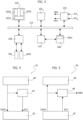
- FIG. 1 shows a typical electronic system, such as the electronic system of a vehicle, comprising a plurality of processing systems 10, such as embedded systems or integrated circuits, e.g., a Field Programmable Gate Array (FPGA), a Digital Signal Processor (DSP) or a micro-controller (e.g., dedicated to the automotive market).
- processing systems 10 such as embedded systems or integrated circuits, e.g., a Field Programmable Gate Array (FPGA), a Digital Signal Processor (DSP) or a micro-controller (e.g., dedicated to the automotive market).
- FPGA Field Programmable Gate Array
- DSP Digital Signal Processor
- micro-controller e.g., dedicated to the automotive market.
- the communication system may include a vehicle control bus, such as a Controller Area Network (CAN) bus, and possibly a multimedia bus, such as a Media Oriented Systems Transport (MOST) bus, connected to vehicle control bus via a gateway.
- vehicle control bus such as a Controller Area Network (CAN) bus
- multimedia bus such as a Media Oriented Systems Transport (MOST) bus
- the processing systems 10 are located at different positions of the vehicle and may include, e.g., an Engine Control Unit, a Transmission Control Unit (TCU), an Anti-lock Braking System (ABS), a Body Control Module (BCM), and/or a navigation and/or multimedia audio system.
- TCU Transmission Control Unit
- ABS Anti-lock Braking System
- BCM Body Control Module
- one or more of the processing systems 10 may also implement real-time control and regulation functions.
- These processing systems are usually identified as Electronic Control Units.
- FIG 2 shows a block diagram of an exemplary digital processing system 10, such as a micro-controller, which may be used as any of the processing systems 10 of Figure 1 .
- the processing system 10 comprises a microprocessor 102, usually the Central Processing Unit (CPU), programmed via software instructions.
- the software executed by the microprocessor 102 is stored in a non-volatile program memory 104, such as a Flash memory or EEPROM.
- the memory 104 is configured to store the firmware of the processing unit 102, wherein the firmware includes the software instructions to be executed by the microprocessor 102.
- the non-volatile memory 104 may also be used to store other data, such as configuration data, e.g., calibration data.
- the microprocessor 102 usually has associated also a volatile memory 104b, such as a Random-Access-Memory (RAM).
- a volatile memory 104b such as a Random-Access-Memory (RAM).
- RAM Random-Access-Memory
- the memory 104b may be used to store temporary data.
- the communication with the memories 104 and/or 104b is performed via one or more memory controllers 100.
- the memory controller(s) 100 may be integrated in the microprocessor 102 or connected to the microprocessor 102 via a communication channel, such as a system bus of the processing system 10.
- the memories 104 and/or 104b may be integrated with the microprocessor 102 in a single integrated circuit, or the memories 104 and/or 104b may be in the form of a separate integrated circuit and connected to the microprocessor 102, e.g., via the traces of a printed circuit board.
- the microprocessor 102 may have associated one or more (hardware) resources/peripherals 106 selected from the group of:
- a dedicated digital components DC may also correspond to a FPGA integrated in the processing system 10.
- the memory 104 may also comprise the program data for such a FPGA.
- the digital processing system 10 may support different functionalities.
- the behavior of the microprocessor 102 is determined by the firmware stored in the memory 104, e.g., the software instructions to be executed by a microprocessor 102 of a micro-controller 10.
- the firmware stored in the memory 104
- processing systems 10 e.g., micro-controllers adapted to be used in automotive applications
- micro-controllers are expected to exhibit an increase in complexity, mainly due to the increasing number of requested functionalities (new protocols, new features, etc.) and to the tight constraints of execution conditions (e.g ., lower power consumption, increased calculation power and speed, etc.).
- multi-core processing systems 10 may be used to execute (in parallel) several of the processing systems 10 shown in Figure 1 , such as several ECUs of a vehicle.
- FIG 3 shows an example of a multi-core processing system 10.
- the processing system 10 comprises a plurality of n processing cores 102 1 ...102 n connected to a (on-chip) communication system 114.
- the processing cores 102 1 ...102 n may be ARM Cortex ® -R52 cores.
- the communication system 114 may comprise one or more bus systems, e.g., based on the Advanced eXtensible Interface (AXI) bus architecture, and/or a Network-on-Chip (NoC).
- AXI Advanced eXtensible Interface
- NoC Network-on-Chip
- each processing core 102 may comprise a microprocessor 1020 and a communication interface 1022 configured to manage the communication between the microprocessor 1020 and the communication system 114.
- the interface 1022 is a master interface configured to forward a given (read or write) request from the microprocessor 1020 to the communication system 114, and forward an optional response from the communication system 114 to the microprocessor 1020.
- the communication interface 1022 may also comprise a slave interface. For example, in this way, a first microprocessor 1020 may send a request to a second microprocessor 1020 (via the communication interface 1022 of the first microprocessor, the communication system 114 and the communication interface 1022 of the second microprocessor).
- each processing core 102 1 ...102 n may also comprise further local resources, such as one or more local memories 1026, usually identified as Tightly Coupled Memory (TCM).
- TCM Tightly Coupled Memory
- the processing cores 102 1 ...102 n are arranged to exchange data with a non-volatile memory 104 and/or a volatile memory 104b.
- these memories are system memories, i.e., shared for the processing cores 102 1 ...102 n .
- each processing core 102 1 ...102 n may, however, comprise one or more additional local memories 1026.
- the processing system 10 may comprise one or more memory controllers 100 configured to connect at least one non-volatile memory 104 and at least one volatile memory 104b to the communication system 114.
- the memories 104 and/or 104b may be integrated in the integrated circuit of the processing system 10 or connected externally to the integrated circuit.
- the processing system 10 may comprise one or more resources 106, such as one or more communication interfaces or co-processors (e.g ., a cryptographic co-processor).
- the resources 106 are usually connected to the communication system 114 via a respective communication interface 1062.
- the communication interface 1062 comprises at least a slave interface.
- a processing core 102 may send a request to a resource 106 and the resource returns given data.
- one or more of the communication interfaces 1062 may also comprise a respective master interface.
- such a master interface may be useful in case the resource has to start a communication in order to exchange data via (read and/or write) request with another circuit connected to the communication system 114, such as a resource 106 or a processing core 102.
- the communication system 114 may indeed comprise an Advanced Microcontroller Bus Architecture (AMBA) High-performance Bus (AHB), and an Advanced Peripheral Bus (APB) used to connect the resources/peripherals 106 to the AMBA AHB bus.
- AMBA Advanced Microcontroller Bus Architecture
- AHB Advanced Peripheral Bus
- a DMA controller 110 may be used to directly exchange data with a memory, e.g., the memory 104b, based on requests received from a resource 106.
- a communication interface IF may directly read data (via the DMA controller 110) from the memory 104b and transmit these data, without having to exchange further data with a processing unit 102.
- a DMA controller 110 may communicate with the memory or memories via the communication system 114 or via one or more dedicated communication channels.
- processing circuits comprise also one or more circuits configured to verify an error correction code (ECC).
- ECC error correction code
- Figures 4 and Figure 5 show a generic processing system 10 comprising a master device 40 and a slave device 42, wherein the master device 40 and the slave device 42 use a conventional ECC protection scheme.
- the master circuit 40 transmits data DATA to the slave device 42.
- the slave device 42 receives the data bits DATA and additional error correction code bits ECC generated by an error correction code generation circuit 44 configured to generate the bits ECC as a function of the data bits DATA.
- the master device 40 may be a processing core 102, in particular a microprocessor 1020, or a DMA controller 110.
- the slave device 42 may be a memory such as a non-volatile memory 104 or a volatile memory, e.g., a RAM memory 104b or a TCM 1026.
- the error correction code generation circuit 44 may be integrated in the memory controller of the memory 42.
- the microprocessor 1020 or DMA controller 110 may send a write request comprising the data DATA via the communication system 114 to the memory controller 100, and/or via a dedicated communication system within the processing core 102 to a memory controller of the TCM 1026.
- the memory controller may then calculate via the respective error correction code generation circuit 44 the bits ECC and write the data bits DATA and the bits ECC to the memory, e.g., to a memory address included in the write request.
- the master circuit 40 receives given data DATA from the slave device 42. Specifically, the slave device 42 provides the data bits DATA and the additional error correction code bits ECC.
- the microprocessor 1020 or DMA controller 110 may send a read request via the communication system 114 to the memory controller 100, and/or via a dedicated communication system within the processing core 102 to a memory controller of the TCM 1026.
- the memory controller may then read the data bits DATA and the bits ECC from the memory, e.g., from a memory address included in the read request, and transmit the data bits DATA to the microprocessor 1020 or DMA controller 110.
- an error detection circuit 46 is configured to verify the bits DATA and ECC, and possibly generate one or more error signals ERR.
- the one or more error signals ERR may be provided to the master circuit 40 and/or a fault collection and error management circuit 120.
- the error detection circuit 46 may be integrated in the memory controller 100. Specifically, in case of a simple error detection circuit 46, this circuit just verifies the correctness of the bits DATA and ECC. However, the error detection circuit 46 may also provide information concerning the position of the error, which thus may be used by an error correction circuit to correct errors in the data bits DATA. Generally, the error correction circuit may be integrated with the error detection circuit in an error detection and correction circuit 46, or the error correction circuit may be a separate circuit. Accordingly, the circuit 46 may indeed provide corrected data bits DATA to the master device 40.
- ECC schemes may also be used for the communications exchanged via the communication system 114.
- a bus master such as the interface 1022 may add ECC bits to a request sent the communication system 1144.
- the receiving slave circuit such as the slave interface 1062, may verify the ECC bits in order to detect errors in the transmitted request.
- ECC bits may be verified via a respective error detection circuit for each of the address, data and control information of a request, or a combination of these information.
- the number K of ECC bits depends on the number N of DATA bits and the ECC scheme, e.g., how many bits can be repaired.
- the circuit 46 is able to detect up to a given number of flipped bits and eventually repair them.
- the adopted ECC scheme is usually able to detect up to two erroneous bits and repair one erroneous bit, so called Single-Error Correct (SEC) Double-Error Detect (DED) Code.
- Figure 6 shows in this respect an embodiment of error detection circuit 46 adapted to be used in a SECDED scheme, e.g ., as used in an ARM Cortex R52 microcontroller.
- the error detection circuit 46 comprises a syndrome calculation circuit 460 configured to:
- the result of this comparison is indicative of the position of the incorrect bit in case of a single bit error.
- the syndrome SYN corresponds to a bit sequence having K bits.
- a logic gate 464 such as a logic OR gate, is used to generate an error signal ERR 1 as a function of the syndrome SYN, i.e., the error signal ERR 1 is asserted when at least one of the bits of the syndrome SYN is asserted.
- the specific implementation of the error detection circuit 46 may depend on the used ECC scheme.
- the syndrome calculation circuit 460 may often be unable to detect double-bit errors.
- the error signal ERR 1 will be asserted both for a single bit error and a double-bit error.
- the error correction code verification circuit 46 may also comprise a circuit 462 configured to specifically detect single bit errors.
- the single bit error detection circuit 46 may verify an even or odd parity, thereby generating a signal SB indicating that a single bit error occurred.
- the bits ECC may comprise one or more dedicated parity bits which may also not be provided to the syndrome calculation circuit 460.
- such single bit error detection circuit 462 may be unable to distinguish between correct data and double bit-errors.
- the error signal ERR 1 (indicating a single-bit error or double-bit error)
- the signal SB (indicating a single bit error)
- the combinational logic circuit comprises an inverter 468 and a logic AND gate 470.
- the error detection circuit 46 may be configured to use the syndrome SYN and the bit SB to generate a single-bit error signature SIG having N+K bits.
- this operation is implemented in the single bit error detection circuit 462.
- the circuit 46/462 is configured to assert the bit of the signal SIG corresponding to the position indicated by the syndrome SYN, while the other bits of the signal SIG are de-asserted.
- a corresponding signal SB may thus be generated via a logic combination of the bits of the signal SIG, e.g., via a logic OR gate 466, because at most only one of the bits of the signal SIG should be asserted.
- ECC schemes may be used in order to generate the bit-flip signature SIG, which could also indicate that more than one bit should be flipped, e.g., in case of a Double-Error Correct code.
- the error signals ERR 1 and ERR 2 could indicate in general that an error occurred (error signals ERR 1 ) and optionally that the error is correctable or not (error signals ERR 2 ).
- the error detection circuit 46 is configured to compare the syndrome SYN with a plurality of reference syndromes, wherein each reference syndrome corresponds to a given bit flip signature SIG.
- the error detection circuit 46 may assert the respective bits of the error signature SIG.
- the error detection circuit would use N + K reference syndromes, each corresponding to a respective single bit error.
- the verification of the reference signatures and the setting of the signature SIG (and the error signals) may be implemented via a combinational logic circuit.
- each reference syndrome associated with a single bit error may also have a unique pattern compared to double bit flip errors.
- the error detection circuit 46 be configured to:
- the signals ERR 1 , ERR 2 and SIG may be provided to an error correction circuit, e.g ., implemented in the memory controller, which thus may:
- error detection and correction circuits may be complex combinational logic circuits, which introduce additional propagation delays in order to verify the bits DATA and ECC.
- these delays in the path between the master circuit 40 and the slave circuit 42 limit the clock frequency in the processing system 10, e.g., the clock frequency of the processing core 102 in case of a TCM 1026, or at least the clock frequency of the communication system 114 in case of communications with the memory controller 100.
- the first solution usually implies a greater area and power consumption
- the second solution results in lower global system performances, in particular in case of TCM memories 1026, which should provide the read/corrected data DATA within one clock cycle.
- one or more of the above objectives is achieved by means of a processing system having the features specifically set forth in the claims that follow.
- Embodiments moreover concern a related integrated circuit, device and method.
- various embodiments of the present disclosure relate to a processing system, e.g ., integrated in an integrated circuit.
- the processing system comprises a master circuit, a slave circuit and an error detection and correction circuit.
- the master circuit may be a microprocessor and the slave circuit may be a Tightly Coupled Memory.
- the microprocessor may be an ARM based microprocessor, such as an ARM Cortex-M7 processor.
- the master circuit is configured to generate a read request comprising an address, wherein the master circuit is configured to signal the read request by asserting a first control signal, such as a request signal.
- the master circuit is also configured to receive N (first) data bits, a second control signal and a third control signal.
- the master circuit is configured to determine the logic level of the second control signal, such as a wait signal, wherein a respective first logic level indicates that the N (first) data bits contain valid data and a respective second logic level indicates that the N (first) data bits do not contain valid data.
- the master circuit is configured to determine the logic level of the third control signal, such as a retry signal, wherein a respective first logic level indicates that the read request should be repeated, and a respective second logic level indicates that the read request should not be repeated. Accordingly, in response to determining that the second control signal has the respective first logic level, the master circuit reads the N (first) data bits and, in response to determining that the third control signal has the respective first logic level, the master circuit repeats the read request.
- the logic level of the third control signal such as a retry signal
- the slave circuit is configured to receive the read request and, in response to determining that the first control signal is asserted, provide N (second) data bits and K ECC bits associated with the address included in the read request.
- the address associated with the read request may corresponds to the address included in the read request, or the processing system may comprise an address decoder configured to determine the address associated with the read request by mapping the address included in the read request.
- the error detection and correction circuit is configured to receive the read request from the master circuit, and the N (second) data bits and the K ECC bits from the slave circuit. Moreover, the error detection and correction circuit is configured to provide the N (first) data bits, the second control signal and the third control signal to the master circuit. Specifically, in various embodiments, the error detection and correction circuit comprises a multiplexer configured to provide the N (first) data bits to the master circuit by selecting the N (second) data bits received from the slave circuit when a selection signal has a respective first logic level and N further (third/corrected) data bits generated by the error detection and correction circuit when the selection signal has a respective second logic level.
- the error detection and correction circuit is configured to generate the N further (third/corrected) data bits by processing the N (second) data bits and the K ECC bits received from the slave circuit in order to determine whether the N (second) data bits do not comprise errors or comprise one or more correctable bit-errors.
- the error detection and correction circuit asserts an error signal and generates a bit-flip signature having the bits asserted in the positions of the one or more correctable bit-errors.
- the error detection and correction circuit may generate the N further (third/corrected) data bits by inverting the bits of the N (second) data bits received from the slave circuit at the positions for which the bits of the bit-flip signature are asserted.
- the error detection and correction circuit comprises a pipelined architecture, whereby the N further (third/corrected) data bits are generated with a delay of one clock cycle with respect to the respective N (second) data bits provided by the slave circuit.
- the pipelined architecture of the error detection and correction circuit may be implemented via a register configured to store the N (second) data bits and the K ECC bits provided by the slave circuit, or a register configured to store the error signal and the bit-flip signature.
- the error detection and correction circuit comprises a memory and a control circuit comprising a first subcircuit and a second subcircuit.
- the first subcircuit is configured to monitor the first control signal in order to detect a read request.
- the first subcircuit determines an address associated with the read request and verifies whether the address associated with the read request is stored to the memory.
- the first subcircuit In response to determining that the address associated with the read request is not stored to the memory, the first subcircuit sets the logic level of the selection signal to the respective first logic level, whereby the multiplexer provides the N (second) data bits received from the slave circuit. Moreover, the first subcircuit sets the logic level of the second control signal to the respective first logic level indicating that the N (first) data bits provided to the master circuit contain valid data.
- the first subcircuit sets the logic level of the second control signal for a clock cycle to the respective second logic level indicating that the N first data bits do not contain valid data. Moreover, the first subcircuit sets the logic level of the selection signal to the respective second logic level, whereby the multiplexer provides the N further (third/corrected) data bits to the master circuit. However, in this case, the first subcircuit sets the logic level of the second control signal only for the following clock cycle to the respective first logic level indicating that the N (first) data bits contain valid data, whereby the master circuit samples the N (first) data bits contain valid data just at the next clock cycle.
- the second subcircuit manages the storing of addresses to the memory.
- the second subcircuit is configured to monitor the error signal. In response to determining that the error signal is asserted, the second subcircuit verifies whether the address associated with the read request is stored to the memory.
- the second subcircuit in response to determining that the address associated with the read request is not stored to the memory, stores the address associated with the read request to the memory. Moreover, the second subcircuit sets the logic level of the third control signal to the respective first logic level indicating that the read request should be repeated.
- the memory may have a given number of memory slots.
- the second subcircuit may manage the memory as a ring memory and store the address associated with the read request to a next memory slot of the ring memory.
- the second subcircuit may associate with each univocal address stored to a given memory slot respective further data, the further data specifying a number of occurrence and/or a last access time.
- the second subcircuit sets the logic level of the third control signal to the respective second logic level indicating that the read request should not be repeated.
- the error detection and correction circuit may also be configured to process the N (second) data bits and the K ECC bits received from the slave circuit in order to determine whether the N second data bits comprise an uncorrectable bit-error, and in response to determining that the N second data bits comprise an uncorrectable bit-errors, asserting a further error signal.
- the second subcircuit in response to determining that the further error signal is asserted, may also set the logic level of the third control signal to the respective first logic level indicating that the read request should be repeated.
- the slave circuit when the processing system generates via the master circuit a first read request including a given address to data comprising errors, the slave circuit provides in a first clock cycle the N (second) data bits and K Error ECC bits associated with the given address. Moreover, the first subcircuit determines that the address associated with the first read request is not stored to the memory, sets the logic level of the selection signal to the respective first logic level, whereby the multiplexer provides the N (second) data bits received from the slave circuit, and sets the logic level of the second control signal to the respective first logic level indicating that the N (first) data bits provided to the master circuit contain valid data.
- the second subcircuit determines then that the error signal is asserted and the address associated with the read request is not stored to the memory, and accordingly stores the address associated with the read request to the memory and sets the logic level of the third control signal to the respective first logic level indicating that the read request should be repeated.
- the processing system in response to the third control signal being set to the respective first logic level, the processing system generates via the master circuit a second read request including the given address, whereby the slave circuit provides in a third clock cycle the N (second) data bits and K Error ECC bits associated with the given address. Moreover, the first subcircuit determines that the address associated with the second read request is stored to the memory and sets the logic level of the second control signal to the respective second logic level indicating that the N first data bits do not contain valid data.
- the first subcircuit sets the logic level of the selection signal to the respective second logic level, whereby the multiplexer provides the N further (third/corrected) data bits, and sets the logic level of the second control signal to the respective first logic level indicating that the N first data bits contain valid data.
- various embodiments of the present disclosure relate to solutions for improving the performance of a processing system 10a comprising an ECC error detection and correction circuit.
- Figure 7 shows an example of a processing system 10a comprising an error detection circuit 46 and an error correction circuit 48.
- a master circuit 40 receives given data DATA from a slave device 42.
- the slave device 42 provides the data bits DATA and the additional error correction code bits ECC.
- the master circuit 40 such as a microprocessor 1020 or DMA controller 110, may be configured to send a read request comprising an address ADR.
- the master device 40 may also generate one or more control signals CTRL.
- the control signal CTRL may indicate that a request is performed, e.g., by using a request signal, and optionally whether a read or write request is performed, e.g., by using a read/write signal.
- the slave device 42 may be:
- the read request may be transmitted, e.g., via the communication system 114 to the memory controller 100, and/or via a dedicated communication system within the processing core 102 to a TCM 1026.
- the slave device 42 associated with the address ADR receives the read request, obtains respective data DATA associated with the address ADR and provides the data DATA to the master circuit 40.
- the memory may return the data stored to a memory location associated with the address ADR.
- the slave device 42 does not only provide the data bits DATA, but also additional ECC bits.
- the ECC bits may be stored together with the respective data bits DATA.
- the processing system 10a comprises also an error detection circuit 46 configured to verify the bits DATA and ECC.
- the error detection circuit 46 is configured to:
- the error detection circuit 46 is configured to generate one or more error signals ERR, wherein the error detection circuit 46 is configured to:
- the error detection circuit 46 generates also the bit-flip signature SIG. Accordingly, in case of a correctable error, the error detection circuit 46 may assert the respective bits of the bit-flip signature SIG associated with the detected reference syndrome.
- the circuits 40, 42 and 46 may thus be made reference to the previous description of Figures 1 to 6 .
- the one or more error signals ERR and the signature SIG are provided to an error correction circuit 48.
- the error correction circuit 48 is configured to generate corrected data CDATA (at least) when the one or more error signals ERR signal a correctable error.
- the error correction circuit 48 may determine the bits of the signature SIG, which are asserted, and generate the signal CDATA by inverting the respective bits of the data signal DATA.
- the error correction circuit 48 may be implemented, e.g ., via N logic XOR gates, wherein each XOR gate receives at input a respective bit of the signal DATA and the signature SIG, and provides at output a respective bit of the signal CDATA.
- the error correction and detection circuit 46/48 may provide to the master circuit 40 a signal RDATA corresponding to:
- one or more of the error signals ERR may also be provided to the master circuit 40.
- the master circuit 40 is configured to receive a signal RETRY which indicates whether the read request failed, i.e., the error detection circuit 46 is configured to assert the signal RETRY when the error detection circuit 46 detects an uncorrectable error, e.g ., a double-bit error in a SECDED scheme.
- the master circuit 40 may be configured to repeat the read request, when the signal RETRY is asserted, e.g ., when the error detection circuit 46 detects an uncorrectable error.
- the error detection and correction circuit 46/48 may be implemented via one or more combinational logic circuits.
- such combinational logic circuits introduce an additional maximum propagation delay in the path between the slave circuit 42 and the master circuit 40, which limits the maximum clock frequency, which can be used by the master circuit 40 in order to sample the data signal RDATA.
- Figure 8 show a modified example, wherein a pipelined architecture is used in order to split the data read operation from the ECC verification operation.
- the processing system 10a comprises a register 52 configured to store the bits DATA and ECC provided by the slave circuit 42 in response to a clock signal CLK, such as the clock signal of the master circuit 40.
- the error detection circuit 46 may operate with the data bits stored to the register 52, and similarly, the master circuit 40 may receive via the signal RDATA either the stored data DATA provided by the register 52, indicated in the following as data DATA', or the corrected data CDATA provided by the error correction circuit.
- the master circuit 40 is configured to receive the data RDATA after two clock cycles (or even more clock cycles, in case other clock cycles are required to transmit the signals DATA and ECC from the slave circuit 42 to the register 52 and/or the signal RDATA from the error detection and correction circuit 46/48 to the master circuit 40).
- the master circuit 40 may generate the read request, as signaled, e.g ., via a request signal REQ, and a control circuit 54 associated with the error detection and correction circuit 46/48 may generate a control signal indicating when the data signal RDATA is valid.
- the control signal may be either:
- the master circuit 40 is configured to read the signal DATA' in response to a clock signal, e.g ., the clock signal CLK, as a function of the signal WAIT and/or ACK.
- the master circuit 40 may store the bits of the signal DATA' to an internal register.
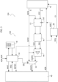
- FIG 9 shows an embodiment of a processing system 10a according to the present disclosure, wherein the processing system 10a comprises again a master circuit 40 and a slave circuit 42.
- the master circuit 40 is again configured to generate a read request comprising an address ADR, wherein the read request is signaled via one or more control signals, such as the previous mentioned request signal REQ. Moreover, the master circuit 40 is configured to receive a data signal RDATA. In order to correctly manage the read request, the master circuit 40 is again configured to receive a control signal indicating whether the data signal RDATA contains valid data, such as the previous mentioned wait signal WAIT (and/or acknowledge signal ACK), i.e. , the master circuit 40 is configured to read the data signal RDATA in response to a clock signal and in response to determining that the control signal WAIT indicates that the data signal RDATA contains valid data.
- a control signal indicating whether the data signal RDATA contains valid data such as the previous mentioned wait signal WAIT (and/or acknowledge signal ACK)
- the master circuit 40 is configured to receive a control signal indicating whether the read request should be repeated, such as the previous mentioned retry signal RETRY.
- the master circuit 40 is a microprocessor 1020.
- the mentioned control signals are often used by an ARM based microprocessor 1020 in order to interface a TCM memory 1026.
- TCM interface protocol of current ARM Cortex processors, such as an ARM Cortex-M7 processor as described, e.g ., in the "Arm Cortex-M7 Processor Technical Reference Manual" , e.g. , Revision r1p2, which is incorporated herein by reference for this purpose
- the slave circuit 42 is configured to receive an address signal ADR and determine respective data bits DATA and respective bits ECC associated with the data bits DATA.
- the slave circuit 42 is a volatile memory, such as a RAM, such as a RAM implementing a TCM memory 1026 of a processing core 102.
- the communication between the master circuit 40 and the slave circuit 42 may be exchanged via any suitable communication system, such as the communication system 114 and/or a dedicated communication system within the processing core 102.
- the address range of the master circuit 40 may indeed be mapped via an address decoder 58 to an address range of the slave circuit 42, such as a physical memory address range of a memory.
- the address decoder 58 may be configured to receive the read request, in particular the address signal ADR and the control signal indicating the request, such as the signal REQ, and may:
- the slave circuit 42 is configured to provide, in response to determining that the signal CS is asserted, the bits DATA and ECC associated with the address ADR'.
- the address decoder 58 may be implemented in the respective communication system and/or in the master circuit 40 and/or in the slave circuit 42.
- the microprocessor 1020 may already provide a physical address ADR of the TCM memory 42 and the request signal REQ may directly correspond to the chip-select) signal CS.
- the address mapping operation is purely optional, and the address decoder 58 may also just be configured - similar to a slave communication interface - to assert the control signal CS once having determined that a given address ADR is associated with the slave circuit 42.
- the processing system 10a comprises moreover an error detection and correction circuit 500.
- the error detection and correction circuit 500 may be associated with:
- the error detection and correction circuit 500 is configured to receive data bits DATA and ECC bits, and generate corrected data CDATA by processing the bits DATA and ECC according to a given ECC scheme. Moreover, the error detection and correction circuit 500 is configured to generate at least one error signal ERR indicating whether the data bits DATA contain errors.
- the error detection and correction circuit 500 may comprise for this purpose an error detection circuit 46 and an error correction circuit 48.
- the error detection and correction circuit 500 has a pipelined architecture, i.e., the error detection and correction circuit 500 comprises at least one register 52.
- the register 52 is configured to receive the bits DATA and ECC from the slave circuit 42 and provided the stored data to the error detection circuit 46.
- the register 52 may also be used to store other signals used for the error detection and correction function, such as the syndrome SYN or the bit-flip signature SIG.
- the content of the corrected data signal CDATA is valid after one clock cycle with respect to the respective bits provided by the slave circuit 42 via the signals DATA and ECC.
- the signal DATA provided by the slave circuit 42 and the corrected data signal CDATA are provided (preferably directly) to a multiplexer 50, i.e., the multiplexer 50 is configured to generate the signal RDATA for the master circuit 40 by selecting the signal DATA provided by the slave circuit when a selection signal SEL has a first value and the signal CDATA provided by the error correction circuit 48 when the selection signal SEL has a second value.
- the signal CDATA will contain valid data just after one further clock cycle.
- the error detection and correction circuit 500 comprises thus also a control circuit 54 configured to receive the read request from the master circuit 40, in particular the address ADR (or the mapped address ADR') and the control signal indicating the read request, such as the request signal REQ or the chip-select signal CS, and the one or more error signal ERR from the error detection circuit 46.
- the control circuit 54 is configured to generate as a function of these signals the wait signal WAIT (or similarly an acknowledge signal ACK) and the retry signal RETRY for the master circuit 40, and the selection circuit SEL for the multiplexer 50.
- the control circuit 54 should be configured to assert the wait signal WAIT (or similarly de-assert an acknowledge ACK) when the one or more error signals ERR indicate an error in the bits DATA and/or ECC, in particular in case of a correctable error, because in this case, the master circuit 40 should read the data CDATA, which are however only valid at the next clock cycle.
- the one or more error signals ERR are possibly only asserted after one clock cycle with respect to the data signal DATA. Accordingly, the error signals ERR cannot be used to directly generate the wait signal WAIT.
- the control circuit 54 is configured to track addresses ADR (or similarly ADR'), for which the error detection and correction circuit 500 had detected ECC errors in the past.
- the addresses with errors may be stored to a memory 56, preferably implemented with registers.
- the memory 56 may comprise a given number of slots, such as 2, 4, 8 or 16 slots, such as slots S1, S2, etc.
- Figure 10 shows an embodiment of the operation of a first sub-circuit of the control circuit 54, which, e.g., may be implemented via a finite state machine, i.e., via a sequential logic circuit.
- the control circuit 54 waits at a step 1102 for a read request.
- the control circuit 54 may be configured to verify at the step 1102 whether the request signal REQ or the chip-select signal CS is asserted for the current clock cycle. In case the control circuit 54 determines that no read request has been received (output "N" of the verification step 1102), the control circuit may thus return to the step 1102.
- control circuit 54 determines that a read request has been received (output "Y" of the verification step 1102)
- the control circuit 54 proceeds to a step 1104, where the control circuit 54 obtains the address ADR (or ADR') of the read request and determines whether the obtained address is stored to the memory 56.
- the control circuit 54 verifies then at a step 1106 whether the obtained address is stored to the memory 56. Specifically, in case the obtained address is not stored to the memory 56 (output "N" of the verification step 1106), the control circuit 54 proceeds to a step 1108 where the control circuit 54 de-asserts the wait signal WAIT (or asserts the acknowledge signal ACK) and sets the selection signal SEL in order to select the signal DATA provided by the slave circuit 40.
- the control circuit 54 proceeds to a step 1110 where the control circuit 54 asserts the wait signal WAIT (or de-asserts the acknowledge signal ACK).
- the control circuit 54 proceeds to a step 1112 where the control circuit 54 de-asserts the wait signal WAIT (or asserts the acknowledge signal ACK) at the next clock cycle, thereby signaling to the master circuit 40 the fact that the master circuit 40 should acquire the data RDATA only at the next cycle, which should correspond to the corrected data CDATA.
- the control circuit 54 sets the selection signal SEL in order to select the signal CDATA provided by the error correction circuit 48.
- the value of the selection signal SEL at the step 1110 is not relevant, because the master circuit 40 should not read the signal RDATA at the step 1110.
- control circuit 54 may return to the step 1102 for processing a next read request.
- read requests to addresses ADR (or ADR') usually not comprising errors may be processed in one clock cycle by directly providing the data DATA to the master circuit.
- read requests to addresses ADR (or ADR') usually comprising errors are processed in two clock cycles by providing the data CDATA to the master circuit.
- the data CDATA refer to corrected data
- these data may also correspond to the original data DATA in case the error detection circuit 46 does not detect errors in the bits DATA and ECC, i.e., in case the bit-flip signature SIG has all bits set to "0".
- Figure 11 shows an embodiment of the operation of a second sub-circuit of the control circuit 54, which implements a parallel process of the control circuit 54.
- the second sub-circuit may be implemented via a sequential logic circuit or just a combinational logic circuit.
- the control circuit 54 waits at a step 1202 whether an error is signaled by the error detection circuit 46, e.g ., whether an error signal ERR is asserted. In case the control circuit 54 determines that no error has been signaled (output "N" of the verification step 1202), the control circuit may thus return to the step 1202.
- control circuit 54 determines whether an error has been signaled (output "Y" of the verification step 1202) is a step 1204. Specifically, at the step 1204, the control circuit 54 determines whether the address ADR (or ADR') associated with the request having generated the error is stored to the memory 56.
- the error signal ERR will only be asserted at the second clock cycle.
- the control circuit 54 determines that the address ADR (or ADR') is not stored to the memory 54, the request may be processed in a single clock cycle. Accordingly, in order to correctly use the address ADR (or ADR') associated with the request having generated the error is stored to the memory 56, the control circuit 54 may be configured to temporary store the address of each read request, e.g., at the step 1104 of Figure 10 . Accordingly, the control circuit 54 may use at the step 1204 the temporary stored address.
- control circuit manages at the step 1204 the storage of the address ADR (or ADR') to the memory 56.
- the control circuit 54 may add the address to the memory 56, e.g., by storing the address ADR (or ADR') to the first slot S1.
- control circuit 54 may use different strategies.
- control circuit 54 may be configured to use the memory as a ring memory, wherein - even in case the memory comprises also the same address - the control circuit 54 simply adds the address to a next memory slot of the memory, wherein the control circuit overwrites the oldest memory slots.
- control circuit 54 is configured to add the addresses, which are not already stored to the memory 56.
- control circuit 54 may also associate further data with each address stored to a memory slot, such as a number of occurrences of errors for the respective address and/or data identifying a time stamp of the last error for the respective address.
- the above additional data may be used by the control circuit 54 in order to decide, e.g ., when the memory 54 is full and/or periodically, whether to clear a given memory slot.
- a given address may also be removed from the memory 56 when the error detection circuit 46 does not signal an error during a following read request.
- control circuit 54 proceeds to a verification step 1206. Specifically, in case the control circuit 54 determines that the address ADR (or ADR') associated with the request having generated the error was already stored to the memory 56 (output "Y" of the verification step 1210), the control circuit 54 already determines at the steps 1104 and 1106 of Figure 10 that two clock cycles are required to provide corrected data.
- control circuit 54 may return to the step for waiting for a further error. Specifically, as schematically shown via a step 1212, in this case the control circuit 54 may de-assert the retry signal RETRY, in order to signal to the master circuit 40 the fact that the master circuit 40 should not repeat the request.
- the error detection and correction circuit 500 may support an ECC code permitting to correct a given number of flipped bits and just detect a higher number of flipped bits, such as a SECDED code.
- the control circuit 54 may proceed to an optional step 1210, where the control circuit 54 verifies the error signal(s) ERR in order to determine whether the error is a correctable or uncorrectable error. Specifically, in case the control circuit determines a correctable error (output "SBE" of the verification step 1210), such as a single bit error, the control circuit 54 may return to the step 1202 via the step 1212.
- control circuit 54 may assert at a step 1208 the retry signal RETRY, in order to signal to the master circuit 40 the fact that the master circuit 40 should repeat the read request and the control circuit 54 may then return to the step 1202.
- control circuit 54 may proceed also to the step 1208.
- the control circuit 54 determines at the steps 1104 and 1106 of Figure 10 that just one clock cycles was required to provide the data DATA, even though indeed the data CDATA would have to be used after two clock cycles.
- the control circuit 54 may assert at the step 1208 the retry signal RETRY, in order to signal to the master circuit 40 the fact that the master circuit 40 should repeat the request.
- the respective address will then be stored to the memory 54 and the control circuit 54 will indicate that two clock cycles are required for the processing of the data via the error detection and correction circuit 500.
- the solutions described in the foregoing permit to access a slave device 42 in a single clock cycle, and just in case errors are associated with specific addresses, the read request to these addresses is performed with two clock cycles in order to permit that the error correction circuit 48 generates corrected data CDATA, which then may be read by the master circuit 40.
Landscapes
- Engineering & Computer Science (AREA)
- Theoretical Computer Science (AREA)
- Physics & Mathematics (AREA)
- General Engineering & Computer Science (AREA)
- General Physics & Mathematics (AREA)
- Human Computer Interaction (AREA)
- Computer Security & Cryptography (AREA)
- Quality & Reliability (AREA)
- Techniques For Improving Reliability Of Storages (AREA)
- Detection And Correction Of Errors (AREA)
Applications Claiming Priority (1)
| Application Number | Priority Date | Filing Date | Title |
|---|---|---|---|
| IT102022000004046A IT202200004046A1 (it) | 2022-03-03 | 2022-03-03 | Sistema di elaborazione, relativo circuito integrato, dispositivo e procedimento |
Publications (2)
| Publication Number | Publication Date |
|---|---|
| EP4239481A1 true EP4239481A1 (de) | 2023-09-06 |
| EP4239481B1 EP4239481B1 (de) | 2024-07-31 |
Family
ID=81580540
Family Applications (1)
| Application Number | Title | Priority Date | Filing Date |
|---|---|---|---|
| EP23156381.8A Active EP4239481B1 (de) | 2022-03-03 | 2023-02-13 | Verarbeitungssystem, zugehörige integrierte schaltung, vorrichtung und verfahren |
Country Status (3)
| Country | Link |
|---|---|
| US (1) | US12386546B2 (de) |
| EP (1) | EP4239481B1 (de) |
| IT (1) | IT202200004046A1 (de) |
Citations (3)
| Publication number | Priority date | Publication date | Assignee | Title |
|---|---|---|---|---|
| US20110099451A1 (en) * | 2009-10-22 | 2011-04-28 | Arm Limited | Error control coding for single error correction and double error detection |
| US20190114236A1 (en) * | 2017-10-12 | 2019-04-18 | Electronics And Telecommunications Research Institute | Fault tolerant network on-chip |
| US20200371862A1 (en) * | 2019-05-24 | 2020-11-26 | Texas Instruments Incorporated | Parallelized scrubbing transactions |
Family Cites Families (6)
| Publication number | Priority date | Publication date | Assignee | Title |
|---|---|---|---|---|
| TWI442406B (zh) * | 2009-07-02 | 2014-06-21 | Silicon Motion Inc | 針對一快閃記憶體的控制器之錯誤管理機制來提升驗證效率之方法以及相關之記憶裝置及其控制器 |
| KR101941270B1 (ko) * | 2012-01-03 | 2019-04-10 | 삼성전자주식회사 | 멀티-레벨 메모리 장치를 제어하는 메모리 제어기 및 그것의 에러 정정 방법 |
| JP2014140111A (ja) * | 2013-01-21 | 2014-07-31 | Sony Corp | コントローラ、情報処理システム、コントローラの制御方法およびプログラム |
| US9501352B2 (en) * | 2014-03-05 | 2016-11-22 | Kabushiki Kaisha Toshiba | Memory device |
| US11762736B2 (en) * | 2021-05-18 | 2023-09-19 | Samsung Electronics Co., Ltd. | Semiconductor memory devices |
| KR20240007996A (ko) * | 2022-07-11 | 2024-01-18 | 삼성전자주식회사 | 반도체 메모리 장치 및 메모리 모듈 |
-
2022
- 2022-03-03 IT IT102022000004046A patent/IT202200004046A1/it unknown
-
2023
- 2023-02-13 EP EP23156381.8A patent/EP4239481B1/de active Active
- 2023-03-02 US US18/116,372 patent/US12386546B2/en active Active
Patent Citations (4)
| Publication number | Priority date | Publication date | Assignee | Title |
|---|---|---|---|---|
| US20110099451A1 (en) * | 2009-10-22 | 2011-04-28 | Arm Limited | Error control coding for single error correction and double error detection |
| US8381083B2 (en) | 2009-10-22 | 2013-02-19 | Arm Limited | Error control coding for single error correction and double error detection |
| US20190114236A1 (en) * | 2017-10-12 | 2019-04-18 | Electronics And Telecommunications Research Institute | Fault tolerant network on-chip |
| US20200371862A1 (en) * | 2019-05-24 | 2020-11-26 | Texas Instruments Incorporated | Parallelized scrubbing transactions |
Non-Patent Citations (1)
| Title |
|---|
| "Single Error Correction and Double Error Detection (SECDED) with CoolRunner IIrM CPLDs", APPLICATION NOTE XAPP383, vol. l, 1 August 2003 (2003-08-01) |
Also Published As
| Publication number | Publication date |
|---|---|
| IT202200004046A1 (it) | 2023-09-03 |
| EP4239481B1 (de) | 2024-07-31 |
| US12386546B2 (en) | 2025-08-12 |
| US20230280933A1 (en) | 2023-09-07 |
Similar Documents
| Publication | Publication Date | Title |
|---|---|---|
| US11764807B2 (en) | Processing system, related integrated circuit, device and method | |
| US7877647B2 (en) | Correcting a target address in parallel with determining whether the target address was received in error | |
| US8516174B2 (en) | Data transmission method between master and slave devices | |
| US8671329B2 (en) | Low overhead and timing improved architecture for performing error checking and correction for memories and buses in system-on-chips, and other circuits, systems and processes | |
| CN104572517B (zh) | 提供被请求数据的方法、控制器以及计算机系统 | |
| EP4141677B1 (de) | Verarbeitungssystem, zugehörige integrierte schaltung, vorrichtung und verfahren | |
| WO2019136595A1 (zh) | 处理i2c总线死锁的方法、电子设备和通信系统 | |
| WO2010069045A1 (en) | Error detection method and a system including one or more memory devices | |
| CN116893930A (zh) | 处理系统、相关集成电路以及设备和方法 | |
| JPH10340212A (ja) | クロック同期バス上の障害を分離する方法 | |
| EP4239481B1 (de) | Verarbeitungssystem, zugehörige integrierte schaltung, vorrichtung und verfahren | |
| CN111858141A (zh) | 系统芯片存储控制装置和系统芯片 | |
| CN116701045A (zh) | 处理系统、相关集成电路、设备和方法 | |
| TW202311891A (zh) | 時脈產生裝置、控制器以及儲存裝置 | |
| CN116560902A (zh) | 处理系统、相关集成电路和方法 | |
| US11888618B2 (en) | Master, slave, master-slave-communication system, on-chip interconnect system, method for operating a master, method for operating a slave, method for operating a master-slave communication system and method for operating an on-chip interconnect system | |
| Malatesta et al. | GRLIB: VHDL IP library for fault-tolerant SOC | |
| US20250225068A1 (en) | Processing system, and related method | |
| US12373282B2 (en) | Processing system, related integrated circuit and method | |
| CN115617565A (zh) | 处理系统、相关集成电路、设备以及方法 | |
| EP4296850B1 (de) | Verarbeitungssystem, zugehörige integrierte schaltung, vorrichtung und verfahren | |
| CN120256342A (zh) | 处理系统和相关方法 | |
| US20250389771A1 (en) | Method for testing a counter, corresponding processing system and computer program product | |
| Jaswanth et al. | A review on FPGA implementation of ECC enabled memory controller using AXI protocol | |
| CN116893936A (zh) | 处理系统、相关集成电路、设备和方法 |
Legal Events
| Date | Code | Title | Description |
|---|---|---|---|
| PUAI | Public reference made under article 153(3) epc to a published international application that has entered the european phase |
Free format text: ORIGINAL CODE: 0009012 |
|
| STAA | Information on the status of an ep patent application or granted ep patent |
Free format text: STATUS: THE APPLICATION HAS BEEN PUBLISHED |
|
| AK | Designated contracting states |
Kind code of ref document: A1 Designated state(s): AL AT BE BG CH CY CZ DE DK EE ES FI FR GB GR HR HU IE IS IT LI LT LU LV MC ME MK MT NL NO PL PT RO RS SE SI SK SM TR |
|
| STAA | Information on the status of an ep patent application or granted ep patent |
Free format text: STATUS: REQUEST FOR EXAMINATION WAS MADE |
|
| 17P | Request for examination filed |
Effective date: 20240226 |
|
| RBV | Designated contracting states (corrected) |
Designated state(s): AL AT BE BG CH CY CZ DE DK EE ES FI FR GB GR HR HU IE IS IT LI LT LU LV MC ME MK MT NL NO PL PT RO RS SE SI SK SM TR |
|
| GRAP | Despatch of communication of intention to grant a patent |
Free format text: ORIGINAL CODE: EPIDOSNIGR1 |
|
| STAA | Information on the status of an ep patent application or granted ep patent |
Free format text: STATUS: GRANT OF PATENT IS INTENDED |
|
| INTG | Intention to grant announced |
Effective date: 20240516 |
|
| GRAS | Grant fee paid |
Free format text: ORIGINAL CODE: EPIDOSNIGR3 |
|
| GRAA | (expected) grant |
Free format text: ORIGINAL CODE: 0009210 |
|
| STAA | Information on the status of an ep patent application or granted ep patent |
Free format text: STATUS: THE PATENT HAS BEEN GRANTED |
|
| AK | Designated contracting states |
Kind code of ref document: B1 Designated state(s): AL AT BE BG CH CY CZ DE DK EE ES FI FR GB GR HR HU IE IS IT LI LT LU LV MC ME MK MT NL NO PL PT RO RS SE SI SK SM TR |
|
| REG | Reference to a national code |
Ref country code: CH Ref legal event code: EP Ref country code: GB Ref legal event code: FG4D |
|
| REG | Reference to a national code |
Ref country code: DE Ref legal event code: R096 Ref document number: 602023000298 Country of ref document: DE |
|
| REG | Reference to a national code |
Ref country code: IE Ref legal event code: FG4D |
|
| REG | Reference to a national code |
Ref country code: LT Ref legal event code: MG9D |
|
| REG | Reference to a national code |
Ref country code: NL Ref legal event code: MP Effective date: 20240731 |
|
| PG25 | Lapsed in a contracting state [announced via postgrant information from national office to epo] |
Ref country code: PT Free format text: LAPSE BECAUSE OF FAILURE TO SUBMIT A TRANSLATION OF THE DESCRIPTION OR TO PAY THE FEE WITHIN THE PRESCRIBED TIME-LIMIT Effective date: 20241202 |
|
| REG | Reference to a national code |
Ref country code: AT Ref legal event code: MK05 Ref document number: 1709120 Country of ref document: AT Kind code of ref document: T Effective date: 20240731 |
|
| PG25 | Lapsed in a contracting state [announced via postgrant information from national office to epo] |
Ref country code: PT Free format text: LAPSE BECAUSE OF FAILURE TO SUBMIT A TRANSLATION OF THE DESCRIPTION OR TO PAY THE FEE WITHIN THE PRESCRIBED TIME-LIMIT Effective date: 20241202 |
|
| PG25 | Lapsed in a contracting state [announced via postgrant information from national office to epo] |
Ref country code: NO Free format text: LAPSE BECAUSE OF FAILURE TO SUBMIT A TRANSLATION OF THE DESCRIPTION OR TO PAY THE FEE WITHIN THE PRESCRIBED TIME-LIMIT Effective date: 20241031 |
|
| PG25 | Lapsed in a contracting state [announced via postgrant information from national office to epo] |
Ref country code: FI Free format text: LAPSE BECAUSE OF FAILURE TO SUBMIT A TRANSLATION OF THE DESCRIPTION OR TO PAY THE FEE WITHIN THE PRESCRIBED TIME-LIMIT Effective date: 20240731 Ref country code: PL Free format text: LAPSE BECAUSE OF FAILURE TO SUBMIT A TRANSLATION OF THE DESCRIPTION OR TO PAY THE FEE WITHIN THE PRESCRIBED TIME-LIMIT Effective date: 20240731 Ref country code: GR Free format text: LAPSE BECAUSE OF FAILURE TO SUBMIT A TRANSLATION OF THE DESCRIPTION OR TO PAY THE FEE WITHIN THE PRESCRIBED TIME-LIMIT Effective date: 20241101 Ref country code: NL Free format text: LAPSE BECAUSE OF FAILURE TO SUBMIT A TRANSLATION OF THE DESCRIPTION OR TO PAY THE FEE WITHIN THE PRESCRIBED TIME-LIMIT Effective date: 20240731 |
|
| PG25 | Lapsed in a contracting state [announced via postgrant information from national office to epo] |
Ref country code: BG Free format text: LAPSE BECAUSE OF FAILURE TO SUBMIT A TRANSLATION OF THE DESCRIPTION OR TO PAY THE FEE WITHIN THE PRESCRIBED TIME-LIMIT Effective date: 20240731 |
|
| PG25 | Lapsed in a contracting state [announced via postgrant information from national office to epo] |
Ref country code: LV Free format text: LAPSE BECAUSE OF FAILURE TO SUBMIT A TRANSLATION OF THE DESCRIPTION OR TO PAY THE FEE WITHIN THE PRESCRIBED TIME-LIMIT Effective date: 20240731 |
|
| PG25 | Lapsed in a contracting state [announced via postgrant information from national office to epo] |
Ref country code: IS Free format text: LAPSE BECAUSE OF FAILURE TO SUBMIT A TRANSLATION OF THE DESCRIPTION OR TO PAY THE FEE WITHIN THE PRESCRIBED TIME-LIMIT Effective date: 20241130 Ref country code: AT Free format text: LAPSE BECAUSE OF FAILURE TO SUBMIT A TRANSLATION OF THE DESCRIPTION OR TO PAY THE FEE WITHIN THE PRESCRIBED TIME-LIMIT Effective date: 20240731 |
|
| PG25 | Lapsed in a contracting state [announced via postgrant information from national office to epo] |
Ref country code: HR Free format text: LAPSE BECAUSE OF FAILURE TO SUBMIT A TRANSLATION OF THE DESCRIPTION OR TO PAY THE FEE WITHIN THE PRESCRIBED TIME-LIMIT Effective date: 20240731 |
|
| PG25 | Lapsed in a contracting state [announced via postgrant information from national office to epo] |
Ref country code: RS Free format text: LAPSE BECAUSE OF FAILURE TO SUBMIT A TRANSLATION OF THE DESCRIPTION OR TO PAY THE FEE WITHIN THE PRESCRIBED TIME-LIMIT Effective date: 20241031 Ref country code: ES Free format text: LAPSE BECAUSE OF FAILURE TO SUBMIT A TRANSLATION OF THE DESCRIPTION OR TO PAY THE FEE WITHIN THE PRESCRIBED TIME-LIMIT Effective date: 20240731 |
|
| PG25 | Lapsed in a contracting state [announced via postgrant information from national office to epo] |
Ref country code: RS Free format text: LAPSE BECAUSE OF FAILURE TO SUBMIT A TRANSLATION OF THE DESCRIPTION OR TO PAY THE FEE WITHIN THE PRESCRIBED TIME-LIMIT Effective date: 20241031 Ref country code: PL Free format text: LAPSE BECAUSE OF FAILURE TO SUBMIT A TRANSLATION OF THE DESCRIPTION OR TO PAY THE FEE WITHIN THE PRESCRIBED TIME-LIMIT Effective date: 20240731 Ref country code: NO Free format text: LAPSE BECAUSE OF FAILURE TO SUBMIT A TRANSLATION OF THE DESCRIPTION OR TO PAY THE FEE WITHIN THE PRESCRIBED TIME-LIMIT Effective date: 20241031 Ref country code: NL Free format text: LAPSE BECAUSE OF FAILURE TO SUBMIT A TRANSLATION OF THE DESCRIPTION OR TO PAY THE FEE WITHIN THE PRESCRIBED TIME-LIMIT Effective date: 20240731 Ref country code: LV Free format text: LAPSE BECAUSE OF FAILURE TO SUBMIT A TRANSLATION OF THE DESCRIPTION OR TO PAY THE FEE WITHIN THE PRESCRIBED TIME-LIMIT Effective date: 20240731 Ref country code: IS Free format text: LAPSE BECAUSE OF FAILURE TO SUBMIT A TRANSLATION OF THE DESCRIPTION OR TO PAY THE FEE WITHIN THE PRESCRIBED TIME-LIMIT Effective date: 20241130 Ref country code: HR Free format text: LAPSE BECAUSE OF FAILURE TO SUBMIT A TRANSLATION OF THE DESCRIPTION OR TO PAY THE FEE WITHIN THE PRESCRIBED TIME-LIMIT Effective date: 20240731 Ref country code: GR Free format text: LAPSE BECAUSE OF FAILURE TO SUBMIT A TRANSLATION OF THE DESCRIPTION OR TO PAY THE FEE WITHIN THE PRESCRIBED TIME-LIMIT Effective date: 20241101 Ref country code: FI Free format text: LAPSE BECAUSE OF FAILURE TO SUBMIT A TRANSLATION OF THE DESCRIPTION OR TO PAY THE FEE WITHIN THE PRESCRIBED TIME-LIMIT Effective date: 20240731 Ref country code: ES Free format text: LAPSE BECAUSE OF FAILURE TO SUBMIT A TRANSLATION OF THE DESCRIPTION OR TO PAY THE FEE WITHIN THE PRESCRIBED TIME-LIMIT Effective date: 20240731 Ref country code: BG Free format text: LAPSE BECAUSE OF FAILURE TO SUBMIT A TRANSLATION OF THE DESCRIPTION OR TO PAY THE FEE WITHIN THE PRESCRIBED TIME-LIMIT Effective date: 20240731 Ref country code: AT Free format text: LAPSE BECAUSE OF FAILURE TO SUBMIT A TRANSLATION OF THE DESCRIPTION OR TO PAY THE FEE WITHIN THE PRESCRIBED TIME-LIMIT Effective date: 20240731 |
|
| PG25 | Lapsed in a contracting state [announced via postgrant information from national office to epo] |
Ref country code: RO Free format text: LAPSE BECAUSE OF FAILURE TO SUBMIT A TRANSLATION OF THE DESCRIPTION OR TO PAY THE FEE WITHIN THE PRESCRIBED TIME-LIMIT Effective date: 20240731 Ref country code: DK Free format text: LAPSE BECAUSE OF FAILURE TO SUBMIT A TRANSLATION OF THE DESCRIPTION OR TO PAY THE FEE WITHIN THE PRESCRIBED TIME-LIMIT Effective date: 20240731 Ref country code: SM Free format text: LAPSE BECAUSE OF FAILURE TO SUBMIT A TRANSLATION OF THE DESCRIPTION OR TO PAY THE FEE WITHIN THE PRESCRIBED TIME-LIMIT Effective date: 20240731 |
|
| PG25 | Lapsed in a contracting state [announced via postgrant information from national office to epo] |
Ref country code: EE Free format text: LAPSE BECAUSE OF FAILURE TO SUBMIT A TRANSLATION OF THE DESCRIPTION OR TO PAY THE FEE WITHIN THE PRESCRIBED TIME-LIMIT Effective date: 20240731 |
|
| PG25 | Lapsed in a contracting state [announced via postgrant information from national office to epo] |
Ref country code: CZ Free format text: LAPSE BECAUSE OF FAILURE TO SUBMIT A TRANSLATION OF THE DESCRIPTION OR TO PAY THE FEE WITHIN THE PRESCRIBED TIME-LIMIT Effective date: 20240731 |
|
| PG25 | Lapsed in a contracting state [announced via postgrant information from national office to epo] |
Ref country code: SK Free format text: LAPSE BECAUSE OF FAILURE TO SUBMIT A TRANSLATION OF THE DESCRIPTION OR TO PAY THE FEE WITHIN THE PRESCRIBED TIME-LIMIT Effective date: 20240731 Ref country code: IT Free format text: LAPSE BECAUSE OF FAILURE TO SUBMIT A TRANSLATION OF THE DESCRIPTION OR TO PAY THE FEE WITHIN THE PRESCRIBED TIME-LIMIT Effective date: 20240731 |
|
| REG | Reference to a national code |
Ref country code: DE Ref legal event code: R097 Ref document number: 602023000298 Country of ref document: DE |
|
| PLBE | No opposition filed within time limit |
Free format text: ORIGINAL CODE: 0009261 |
|
| STAA | Information on the status of an ep patent application or granted ep patent |
Free format text: STATUS: NO OPPOSITION FILED WITHIN TIME LIMIT |
|
| 26N | No opposition filed |
Effective date: 20250501 |
|
| PG25 | Lapsed in a contracting state [announced via postgrant information from national office to epo] |
Ref country code: SE Free format text: LAPSE BECAUSE OF FAILURE TO SUBMIT A TRANSLATION OF THE DESCRIPTION OR TO PAY THE FEE WITHIN THE PRESCRIBED TIME-LIMIT Effective date: 20240731 |
|
| PG25 | Lapsed in a contracting state [announced via postgrant information from national office to epo] |
Ref country code: MC Free format text: LAPSE BECAUSE OF FAILURE TO SUBMIT A TRANSLATION OF THE DESCRIPTION OR TO PAY THE FEE WITHIN THE PRESCRIBED TIME-LIMIT Effective date: 20240731 |
|
| PG25 | Lapsed in a contracting state [announced via postgrant information from national office to epo] |
Ref country code: LU Free format text: LAPSE BECAUSE OF NON-PAYMENT OF DUE FEES Effective date: 20250213 |
|
| REG | Reference to a national code |
Ref country code: BE Ref legal event code: MM Effective date: 20250228 |
|
| PG25 | Lapsed in a contracting state [announced via postgrant information from national office to epo] |
Ref country code: FR Free format text: LAPSE BECAUSE OF NON-PAYMENT OF DUE FEES Effective date: 20250228 |
|
| PG25 | Lapsed in a contracting state [announced via postgrant information from national office to epo] |
Ref country code: BE Free format text: LAPSE BECAUSE OF NON-PAYMENT OF DUE FEES Effective date: 20250228 |
|
| PG25 | Lapsed in a contracting state [announced via postgrant information from national office to epo] |
Ref country code: IE Free format text: LAPSE BECAUSE OF NON-PAYMENT OF DUE FEES Effective date: 20250213 |
|
| PGFP | Annual fee paid to national office [announced via postgrant information from national office to epo] |
Ref country code: DE Payment date: 20260121 Year of fee payment: 4 |