EP4236337A2 - Electronic equipment, imaging device, and mobile body - Google Patents
Electronic equipment, imaging device, and mobile body Download PDFInfo
- Publication number
- EP4236337A2 EP4236337A2 EP23181996.2A EP23181996A EP4236337A2 EP 4236337 A2 EP4236337 A2 EP 4236337A2 EP 23181996 A EP23181996 A EP 23181996A EP 4236337 A2 EP4236337 A2 EP 4236337A2
- Authority
- EP
- European Patent Office
- Prior art keywords
- circuit board
- electronic
- enclosure portion
- electronic apparatus
- electronic components
- Prior art date
- Legal status (The legal status is an assumption and is not a legal conclusion. Google has not performed a legal analysis and makes no representation as to the accuracy of the status listed.)
- Withdrawn
Links
- 238000003384 imaging method Methods 0.000 title claims description 38
- 238000005192 partition Methods 0.000 claims description 58
- 239000004020 conductor Substances 0.000 claims description 21
- 230000017525 heat dissipation Effects 0.000 description 17
- 230000003287 optical effect Effects 0.000 description 10
- 239000000758 substrate Substances 0.000 description 8
- 239000007769 metal material Substances 0.000 description 7
- 239000000470 constituent Substances 0.000 description 2
- 238000010276 construction Methods 0.000 description 2
- 238000010586 diagram Methods 0.000 description 2
- 238000004519 manufacturing process Methods 0.000 description 2
- 238000012986 modification Methods 0.000 description 2
- 230000004048 modification Effects 0.000 description 2
- 230000002093 peripheral effect Effects 0.000 description 2
- 241001124569 Lycaenidae Species 0.000 description 1
- 239000000853 adhesive Substances 0.000 description 1
- 230000001070 adhesive effect Effects 0.000 description 1
- 230000004323 axial length Effects 0.000 description 1
- 239000011230 binding agent Substances 0.000 description 1
- 239000003990 capacitor Substances 0.000 description 1
- 230000000295 complement effect Effects 0.000 description 1
- 230000000694 effects Effects 0.000 description 1
- 238000009432 framing Methods 0.000 description 1
- 229910044991 metal oxide Inorganic materials 0.000 description 1
- 150000004706 metal oxides Chemical class 0.000 description 1
- 239000004065 semiconductor Substances 0.000 description 1
- 238000005476 soldering Methods 0.000 description 1
- 238000006467 substitution reaction Methods 0.000 description 1
- 230000001629 suppression Effects 0.000 description 1
Images






Classifications
-
- H—ELECTRICITY
- H04—ELECTRIC COMMUNICATION TECHNIQUE
- H04N—PICTORIAL COMMUNICATION, e.g. TELEVISION
- H04N23/00—Cameras or camera modules comprising electronic image sensors; Control thereof
- H04N23/50—Constructional details
- H04N23/52—Elements optimising image sensor operation, e.g. for electromagnetic interference [EMI] protection or temperature control by heat transfer or cooling elements
-
- G—PHYSICS
- G03—PHOTOGRAPHY; CINEMATOGRAPHY; ANALOGOUS TECHNIQUES USING WAVES OTHER THAN OPTICAL WAVES; ELECTROGRAPHY; HOLOGRAPHY
- G03B—APPARATUS OR ARRANGEMENTS FOR TAKING PHOTOGRAPHS OR FOR PROJECTING OR VIEWING THEM; APPARATUS OR ARRANGEMENTS EMPLOYING ANALOGOUS TECHNIQUES USING WAVES OTHER THAN OPTICAL WAVES; ACCESSORIES THEREFOR
- G03B17/00—Details of cameras or camera bodies; Accessories therefor
- G03B17/55—Details of cameras or camera bodies; Accessories therefor with provision for heating or cooling, e.g. in aircraft
-
- H—ELECTRICITY
- H04—ELECTRIC COMMUNICATION TECHNIQUE
- H04N—PICTORIAL COMMUNICATION, e.g. TELEVISION
- H04N23/00—Cameras or camera modules comprising electronic image sensors; Control thereof
- H04N23/50—Constructional details
- H04N23/51—Housings
-
- H—ELECTRICITY
- H05—ELECTRIC TECHNIQUES NOT OTHERWISE PROVIDED FOR
- H05K—PRINTED CIRCUITS; CASINGS OR CONSTRUCTIONAL DETAILS OF ELECTRIC APPARATUS; MANUFACTURE OF ASSEMBLAGES OF ELECTRICAL COMPONENTS
- H05K7/00—Constructional details common to different types of electric apparatus
- H05K7/02—Arrangements of circuit components or wiring on supporting structure
- H05K7/04—Arrangements of circuit components or wiring on supporting structure on conductive chassis
-
- H—ELECTRICITY
- H05—ELECTRIC TECHNIQUES NOT OTHERWISE PROVIDED FOR
- H05K—PRINTED CIRCUITS; CASINGS OR CONSTRUCTIONAL DETAILS OF ELECTRIC APPARATUS; MANUFACTURE OF ASSEMBLAGES OF ELECTRICAL COMPONENTS
- H05K7/00—Constructional details common to different types of electric apparatus
- H05K7/20—Modifications to facilitate cooling, ventilating, or heating
- H05K7/2039—Modifications to facilitate cooling, ventilating, or heating characterised by the heat transfer by conduction from the heat generating element to a dissipating body
-
- H—ELECTRICITY
- H05—ELECTRIC TECHNIQUES NOT OTHERWISE PROVIDED FOR
- H05K—PRINTED CIRCUITS; CASINGS OR CONSTRUCTIONAL DETAILS OF ELECTRIC APPARATUS; MANUFACTURE OF ASSEMBLAGES OF ELECTRICAL COMPONENTS
- H05K9/00—Screening of apparatus or components against electric or magnetic fields
- H05K9/0007—Casings
- H05K9/002—Casings with localised screening
- H05K9/0022—Casings with localised screening of components mounted on printed circuit boards [PCB]
- H05K9/0037—Housings with compartments containing a PCB, e.g. partitioning walls
Definitions
- the present disclosure relates to an electronic apparatus, an imaging apparatus, and a mobile body.
- An electronic apparatus includes a first circuit board, a second circuit board, one or more electronic components, an enclosure portion, and a housing.
- the one or more electronic components are mounted on at least one of opposing surfaces of the first circuit board and the second circuit board that oppose each other.
- the enclosure portion supports a surface of each of the first circuit board and the second circuit board to oppose each other with a predetermined gap therebetween.
- the enclosure portion encloses a gap space that includes the one or more electronic components within a space between the first circuit board and the second circuit board.
- the housing accommodates the first circuit board, the second circuit board, and the enclosure portion. The enclosure portion contacts the housing.
- An imaging apparatus includes an electronic apparatus.
- the electronic apparatus includes a first circuit board, a second circuit board, one or more electronic components, an enclosure portion, and a housing.
- the one or more electronic components are mounted on at least one of opposing surfaces of the first circuit board and the second circuit board that oppose each other.
- the enclosure portion supports a surface of each of the first circuit board and the second circuit board to oppose each other with a predetermined gap therebetween.
- the enclosure portion encloses a gap space that includes the one or more electronic components within a space between the first circuit board and the second circuit board.
- the housing accommodates the first circuit board, the second circuit board, and the enclosure portion.
- the enclosure portion contacts the housing.
- a mobile body includes an electronic apparatus.
- the electronic apparatus includes a first circuit board, a second circuit board, one or more electronic components, an enclosure portion, and a housing.
- the one or more electronic components are mounted on at least one of opposing surfaces of the first circuit board and the second circuit board that oppose each other.
- the enclosure portion supports a surface of each of the first circuit board and the second circuit board to oppose each other with a predetermined gap therebetween.
- the enclosure portion encloses a gap space that includes the one or more electronic components within a space between the first circuit board and the second circuit board.
- the housing accommodates the first circuit board, the second circuit board, and the enclosure portion.
- the enclosure portion contacts the housing.
- apparatuses having electronic components mounted therein With the increased performance of apparatuses having electronic components mounted therein, it is necessary for apparatuses to house a plurality of substrates having respective electronic components mounted thereon.
- providing a heat absorbing member to each of the electronic components mounted on the plurality of substrates increases the number of elements and hinders miniaturization of the apparatuses.
- the present disclosure aims to provide an electronic apparatus, an imaging apparatus, and a mobile body that can be downsized while maintaining effective heat dissipation.
- the imaging apparatus 10 may be mounted on a mobile body 50 in a manner so as to be able to image a scene surrounding the mobile body 50.
- the mobile body 50 may encompass, for example, vehicles, ships, and aircrafts.
- Vehicles may include, for example, automobiles, industrial vehicles, rail vehicles, domestic vehicles, and fixed-wing aircrafts that travel on a runway.
- Automobiles may include, for example, cars, trucks, buses, motorcycles, and trolley buses.
- Industrial vehicles may include, for example, agricultural vehicles and construction vehicles.
- Industrial vehicles may include, for example, forklifts and golf carts.
- Industrial vehicles for agricultural purpose may include, for example, tractors, tillers, transplanters, binders, combined harvesters, and lawn mowers.
- Industrial vehicles for construction purpose may include, for example, bulldozers, scrapers, excavators, crane trucks, dump trucks, and load rollers.
- Vehicles may include human-powered vehicles that travel on human power. Classification of the vehicles is not limited to the above.
- vehicles may include industrial vehicles authorized to travel on the road.
- a plurality of categories may include the same type of vehicles.
- Vessels may include, for example, watercraft, boats, and tankers.
- Aircraft may include, for example, fixed wing aircraft and rotorcraft.
- the imaging apparatus 10 includes a first electronic apparatus 11 and a second electronic apparatus (electronic apparatus) 12.
- an optical axis direction of a lens which will be described later, will be referred to as an x-direction
- a normal direction of a first circuit board 17 and a second circuit board 18, which will be described later will be referred to as a y-direction
- a direction perpendicular to the x-direction and the y-direction will be referred to as an x-direction.
- the first electronic apparatus 11 includes an imaging optical system 13, an image sensor 14, an image sensor substrate 15, and a first housing 16.
- the imaging optical system 13 includes one or more lenses.
- the imaging optical system 13 is fixed to the first housing 16 such that an optical axis OX of the imaging optical system 13 is perpendicular to an imaging surface of the image sensor 14.
- the imaging optical system 13 forms light incident from a subject as a subject image on the imaging surface of the image sensor 14.
- the image sensor 14 generates an image including the subject image formed on the imaging surface by the imaging optical system 13.
- the image sensor 14 is, for example, a CMOS (Complementary Metal Oxide Semiconductor) image sensor or a CCD (Charge Coupled Device).
- the image sensor 14 is mounted on the image sensor substrate 15.
- the image sensor substrate 15 is a plate-like member.
- the image sensor substrate 15 has the image sensor 14 and the like mounted thereon.
- the first housing 16 houses the imaging optical system 13 and the image sensor substrate 15 having the image sensor 14 mounted thereon.
- the second electronic apparatus 12 performs image processing on the image generated by the first electronic apparatus 11.
- the second electronic apparatus 12 may send a signal to the first electronic apparatus 11, based on the image processing.
- the second electronic apparatus 12 includes a first circuit board 17, a second circuit board 18, electronic components 19, an enclosure portion 20, and a second housing (housing) 21.
- the second electronic apparatus 12 may further include a first shield portion 26 and a second shield portion 27.
- the first circuit board 17 and the second circuit board 18 are plate-like members.
- the first circuit board 17 and the second circuit board 18 are arranged such that respective surfaces of each oppose each other in parallel.
- the electronic components 19 are components constituting an electronic circuit.
- the electronic component 19 include, for example, resistors, capacitors, diodes, or an integrated circuit including these elements.
- the electronic components 19 include at least one of a first electronic component 22 and a second electronic component 23.
- the electronic components 19 may include a third electronic component 24 and a fourth electronic component 25.
- At least one of the electronic components 19 is mounted on at least one of a first opposing surface 17a and a second opposing surface 18a, which will be described later.
- the first electronic component 22 is mounted on the first opposing surface 17a of the first circuit board 17.
- the second electronic component 23 is mounted on the second opposing surface 18a of the second circuit board 18.
- the first electronic component 22 and the second electronic component 23 are arranged within the second electronic apparatus 12 in a manner so as to not interfere with each other.
- the third electronic component 24 may be mounted on a surface of the first circuit board 17 which is opposite from the first opposing surface 17a.
- the fourth electronic component 25 may be mounted on a surface of the second circuit board 18 which is opposite from the second opposing surface 18a.
- the enclosure portion 20 supports the first circuit board 17 and the second circuit board 18 such that one surface of the first circuit board 17 and one surface of the second circuit board 18 oppose each other with a predetermined gap therebetween.
- the enclosure portion 20 encloses a space that includes the first electronic component 22 and the second electronic component 23 within a space between the first circuit board 17 and the second circuit board 18.
- the enclosure portion 20 is, for example, a tubular member as illustrated in FIG. 3 .
- the enclosure portion 20 has a rectangular tube shape that frames a rectangular flat plate.
- the enclosure portion 20 may be formed by a single member in which a plurality of flat plates are integrally formed.
- the enclosure portion 20 may be formed by a member in which a plurality of members are fixed to one another. In the present embodiment, the enclosure portion 20 is formed by a single member.
- the enclosure portion 20 fixes the first circuit board 17 and the second circuit board 18 at end portions thereof in an axial direction (the y-direction in FIG. 2 ).
- the enclosure portion 20 fixes peripheral edge portions of the first opposing surface 17a of the first circuit board 17 at end surfaces 20a arranged in the axial direction (the y-direction in FIG. 2 ) of the rectangular tube.
- the first opposing surface 17a is a surface of the first circuit board 17 that opposes the second circuit board 18.
- the enclosure portion 20 is fixed to peripheral edge portions of the second opposing surface 18a of the second circuit board 18 at end surfaces 20b arranged in the axial direction (the y-direction in FIG. 2 ) of the rectangular tube.
- the second opposing surface 18a is a surface of the second circuit board 18 that opposes the first circuit board 17.
- the enclosure portion 20 fixes the first circuit board 17 and the second circuit board 18 via an adhesive, soldering, a screw, or the like. As a result, the enclosure portion 20 supports the first circuit board 17 and the second circuit board 18 with a predetermined gap therebetween.
- the predetermined gap corresponds to an axial length of the enclosure portion 20.
- the enclosure portion 20 may have heat conductivity.
- the enclosure portion 20 may have electrical conductivity.
- the enclosure portion 20 may be formed from a metal material.
- the enclosure portion 20 may be grounded to the ground of at least one of the first circuit board 17 and the second circuit board 18.
- the first shield portion 26 can improve the electromagnetic compatibility (EMC) of the third electronic component 24.
- the first shield portion 26 shields the third electronic component 24 and can be fixed to the first circuit board 17.
- the second shield portion 27 can improve the electromagnetic compatibility of the fourth electronic component 25.
- the second shield portion 27 shields the fourth electronic component 25 and can be fixed to the second circuit board 18.
- Each of the first shield portion 26 and the second shield portion 27 is formed from a conductive material.
- the second housing 21 houses the first circuit board 17 having the first electronic component 22 mounted thereon, the second circuit board 18 having the second electronic component 23 mounted thereon, and the enclosure portion 20 supporting the first circuit board 17 and the second circuit board 18.
- the second housing 21 contacts at least a part of the enclosure portion 20 and fixes the enclosure portion 20 housed within the second housing 21.
- the second housing 21 may have a fitting structure to fix the enclosure portion 20.
- the second housing 21 includes guide portions 28 provided on the inner wall surface 21a.
- the enclosure portion 20 has external surfaces provided with fitting portions 29 to be fitted into the guide portions 28.
- the fitting portions 29 are guided by the guide portions 28, and thus the enclosure portion 20 is housed within the second housing 21.
- the second housing 21 has opening walls 21b formed in the second housing 21.
- the enclosure portion 20 has protrusions 30 to be fitted into openings 21c defined by the opening walls 21b.
- the protrusions 30 are fitted into the openings 21c, and thus the enclosure portion 20 is housed within the second housing 21.
- the enclosure portion 20 contacts the second housing 21 and, simultaneously, encloses a space that includes one or more of the electronic components 19 within the space between the first circuit board 17 and the second circuit board 18.
- the enclosure portion 20 can absorb heat generated by the electronic components 19 and dissipate the heat to the outside via the second housing 21.
- the second electronic apparatus 12 can improve the heat dissipation effectiveness for heat generated by the electronic components 19.
- the second electronic apparatus 12 requires fewer components than a case in which respective heat absorbing members are provided to the electronic components 19 mounted on the two circuit boards, the second electronic apparatus 12 can be miniaturized.
- the enclosure portion 20 has electrical conductivity and is grounded to the ground of at least one of the first circuit board 17 and the second circuit board 18.
- the enclosure portion 20 can improve the electromagnetic compatibility of the electronic components 19.
- the third electronic component 24 is mounted on the surface of the first circuit board 17 which is opposite from the first opposing surface 17a.
- the first shield portion 26 that can be fixed to the enclosure portion 20 shields the third electronic component 24.
- the second electronic apparatus 12 can allow mounting of more electronic components 19 without increasing the number of circuit boards and further reduce leakage of electromagnetic waves generated by the electronic components 19.
- the second electronic apparatus 12 can improve electromagnetic wave suppression effectiveness and suppress a size increase thereof while allowing the mounting of many electronic components 19.
- an imaging apparatus 100 according to a second embodiment of the present disclosure will be described.
- the second embodiment will be described below, focusing on its features which differ from those of the first embodiment.
- Components having the same configurations as those of the first embodiment are denoted by the same reference numerals.
- the imaging apparatus 100 includes the first electronic apparatus 11 and a second electronic apparatus (electronic apparatus) 120.
- the first electronic apparatus 11 has the same structure and function as those of the first embodiment.
- the second electronic apparatus 120 includes the first circuit board 17, the second circuit board 18, electronic components 19, the enclosure portion 20, and the second housing 21.
- the structures and functions of the first circuit board 17, the second circuit board 18, the electronic components 19, the enclosure portion 20, and the second housing 21 of the second electronic apparatus 120 are the same as those of the first embodiment.
- the second electronic apparatus 120 further includes a partition wall 31.
- the partition wall 31 is, for example, a plate-like member.
- the partition wall 31 has a rectangular shape.
- the partition wall 31 partitions a space between the first circuit board 17 and the second circuit board 18 into a space that includes the first electronic component 22 and a space that includes the second electronic component 23.
- the partition wall 31 may be formed by a single member that is integrally formed with the enclosure portion 20.
- the partition wall 31 may be configured to be a member separate from the enclosure portion 20 and fixed to the enclosure portion 20.
- the partition wall 31 is integrally formed with the enclosure portion 20 at any portion between both ends in the axial direction of the enclosure portion 20, as illustrated in FIG. 6 and FIG. 7 .
- the partition wall 31 is integrally formed at a portion including a midpoint of the end surface 20a and the end surface 20b, this is not restrictive.
- the partition wall 31 may be integrally formed at any portion between both ends of the enclosure portion 20.
- the partition wall 31 may have heat conductivity.
- the partition wall 31 may have electrical conductivity.
- the partition wall 31 may be formed from a metal material.
- the partition wall 31 may directly contact at least one of the first electronic component 22 and the second electronic component 23. Also, the partition wall 31 may indirectly contact at least one of the first electronic component 22 and the second electronic component 23 via a heat conductor 34.
- the second electronic apparatus 120 at least one of the electronic components 19 is provided on at least one of the first opposing surface 17a and the second opposing surface 18a, in the same manner as the first embodiment.
- the enclosure portion 20 contacts the second housing 21 and, simultaneously, encloses the space that includes one or more of the electronic components 19 within the space between the first circuit board 17 and the second circuit board 18.
- the second electronic apparatus 120 can improve heat dissipation effectiveness for heat generated by the electronic components 19.
- the second electronic apparatus 120 can improve the heat dissipation effectiveness with fewer elements than that of a case in which a heat absorbing member is provided for each of the electronic components 19 mounted on the two circuit boards.
- the partition wall 31 partitions the space between the first circuit board 17 and the second circuit board 18 into the space that includes the first electronic component 22 and the space that includes the second electronic component 23.
- the partition wall 31 can suppress the conduction of heat generated by the first electronic component 22 to the second electronic component 23 and enable heat dissipation to the outside of the second housing 21 via the enclosure portion 20.
- the partition wall 31 can suppress the conduction of heat generated by the second electronic component 23 to the first electronic component 22 and enable heat dissipation to the outside of the second housing 21 via the enclosure portion 20.
- the second electronic apparatus 120 can further improve the heat dissipation effectiveness.
- the partition wall 31 shields both electromagnetic waves that are generated by the first electronic component 22 and propagate towards the second electronic component 23 and electromagnetic waves that are generated by the second electronic component 23 and propagate towards the first electronic component 22. Accordingly, the second electronic apparatus 120 can improve electromagnetic compatibility of each of the first electronic component 22 and the second electronic component 23.
- the partition wall 31 directly or indirectly contacts the first electronic component 22.
- the partition wall 31 conducts the heat generated from the first electronic component 22 to the second housing 21 in contact with the partition wall 31, for heat dissipation.
- the second electronic apparatus 120 can more efficiently conduct heat to the second housing 21 than a case in which the first electronic component 22 does not contact the partition wall 31, and thus improve the heat dissipation effect.
- the second electronic apparatus 120 further includes the heat conductors 34 in contact with the partition wall 31 and the electronic components 19.
- the first electronic component 22 and the second electronic component 23 may not necessarily contact the partition wall 31.
- at least one of the first electronic component 22 and the second electronic component 23 that may not necessarily come into direct contact with the partition wall 31 contacts the partition wall 31 via the heat conductor 34.
- the heat conductors 34 can efficiently conduct heat generated from at least one of the first electronic component 22 and the second electronic component 23 via the partition wall 31. Accordingly, the second electronic apparatus 120 can efficiently dissipate heat generated by at least one of the first electronic component 22 and the second electronic component 23.
- an imaging apparatus 101 according to a third embodiment of the present disclosure will be described.
- the third embodiment will be described below, focusing on its features which differ from those of the first embodiment.
- Components having the same configurations as those of the first embodiment are denoted by the same reference numerals.
- the imaging apparatus 101 includes the first electronic apparatus 11 and a second electronic apparatus (electronic apparatus) 121.
- the first electronic apparatus 11 has the same configuration and function as those of the first embodiment.
- the second electronic apparatus 121 includes the first circuit board 17, the second circuit board 18, one or more electronic components 19, the enclosure portion 20, and the second housing 21.
- the structures and functions of the first circuit board 17, the second circuit board 18, the electronic components 19, the enclosure portion 20, and the second housing 21 of the second electronic apparatus 121 are the same as those of the first embodiment.
- the second electronic apparatus 121 further includes first convex support portions 32 and second convex support portions 33.
- the second electronic apparatus 121 may further include a first shield portion 260, a second shield portion 270, and the partition wall 31.
- the partition wall 31 is the same as that of the second embodiment.
- the first convex support portions 32 are arranged in the space enclosed by the enclosure portion 20.
- the first convex support portions 32 are arranged on one side of the partition wall 31.
- Each of the first convex support portions 32 may be formed by a single member integrally formed with the partition wall 31.
- the partition wall 31 may be configured as a member separate from the enclosure portion 20 and fixed to the enclosure portion 20.
- the second electronic apparatus 121 has three first convex support portions 32.
- the three first convex support portions 32 are arranged in such a manner that one of them deviates from a straight line connecting the other two of the first convex support portions 32.
- the first convex support portions 32 is arranged at each of two adjacent corners of a rectangle enclosed by the enclosure portion 20 and a position on a side opposite from a side located between the two adjacent corners.
- Each of the three first convex support portions 32 has a flat surface on its side for supporting the first circuit board 17.
- Each of the three first convex support portions 32 fixes the first circuit board 17 on the flat surface. In this way, the three first convex support portions 32 support the first circuit board 17 within a plane including end portions of the three first convex support portions 32.
- the second electronic apparatus 121 may include one first convex support portion 32.
- the first convex support portion 32 has a plane perpendicular to the axial direction (the y-direction in FIG. 9 ) of the enclosure portion 20.
- the first convex support portion 32 supports the first circuit board 17 by fixing it to the plane.
- the number of the first convex support portions 32 included in the second electronic apparatus 121 may be two, four, or more.
- an axial height h1 of the first convex support portion 32 is less than a height h2 from the partition wall 31 to the end surface 20a in the axial direction of the enclosure portion 20.
- the second convex support portions 33 have a function and a configuration that are similar to those of the first convex support portion 32.
- the second convex support portions 33 are different from the first convex support portions 32, in terms of being arranged on the surface of the partition wall 31 on the opposite side from the surface on which the first convex support portion 32 is arranged.
- a height h3 in the axial direction of the first convex support portion 32 is lower than a height h4 from the partition wall 31 to the axial end surface 20a of the enclosure portion 20, in a manner similar to the first convex support portion 32.
- the first convex support portion 32 and the second convex support portion 33 support the first circuit board 17 and the second circuit board 18 with a predetermined gap therebetween, in such a manner that one surface of the first circuit board 17 and one surface of the second circuit board 18 oppose each other.
- the predetermined gap is a sum of the height h1 of the first convex support portion 32, the height h3 of the second convex support portion 33, and a thickness h5 of the partition wall 31.
- the first shield portion 260 and the second shield portion 270 can improve the electromagnetic compatibility of the third electronic component 24 and the fourth electronic component 25, respectively, in a manner similar to the first embodiment.
- the first shield portion 260 can be fixed to the end surface 20a of the enclosure portion 20.
- the second shield portion 270 can be fixed to the end surface 20b of the enclosure portion 20.
- the first shield portion 260 and the second shield portion 270 are, for example, plate-like members. In particular, each of the first shield portion 260 and the second shield portion 270 has a rectangular shape.
- the first shield portion 260 can shield the third electronic component 24.
- the second shield portion 270 can shield the fourth electronic component 25.
- the second electronic apparatus 121 at least one of the electronic components 19 is provided on at least one of the first opposing surface 17a and the second opposing surface 18a, in a manner the same as the first embodiment.
- the enclosure portion 20 contacts the second housing 21 and, simultaneously, encloses a space that includes one or more electronic components 19 in the space between the first circuit board 17 and the second circuit board 18.
- the second electronic apparatus 121 can improve the heat dissipation effectiveness for heat radiated from the electronic component 19.
- the second electronic apparatus 121 can improve the heat dissipation effectiveness with a smaller number of elements than that of a case in which a heat absorbing member is provided for each of the electronic components 19 mounted on the two circuit boards.
- an imaging apparatus 102 according to a fourth embodiment of the present disclosure will be described.
- the fourth embodiment will be described below, focusing on its features which differ from those of the first embodiment.
- Components having the same configurations as those of the first embodiment are denoted by the same reference numerals.
- the imaging apparatus 102 includes the first electronic apparatus 11 and a second electronic apparatus (electronic apparatus) 122.
- the first electronic apparatus 11 has the same configuration and function as that of the first embodiment.
- the second electronic apparatus 122 includes the first circuit board 17, the second circuit board 18, one or more electronic components 19, and the second housing 21.
- the configurations and functions of the first circuit board 17, the second circuit board 18, the electronic components 19, and the second housing 21 of the second electronic apparatus 122 are the same as those of the first embodiment.
- the second electronic apparatus 122 further includes a first shield portion 35, two second shield portions 36, a first convex support portion 320, and a second convex support portion 330.
- the first shield portion 35 has two first wall portions 37 and a connection portion 38.
- Each of the first wall portions 37 is, for example, a plate-like member.
- each of the first wall portions 37 has a rectangular shape.
- a longitudinal length (in the x-direction in FIG. 11 ) of each of the first wall portions 37 is equal to or longer than a length of a first side of each of the surfaces of the first circuit board 17 and the second circuit board 18.
- the first wall portions 37 may have heat conductivity.
- the first wall portions 37 may have electrical conductivity.
- the first wall portions 37 may be formed from a metal material.
- connection portion 38 supports the two first wall portions 37 with a predetermined gap therebetween.
- the connection portion 38 supports the two first wall portions 37 such that they are in parallel with each other.
- the predetermined gap is equal to or longer than a length of a second side orthogonal to the first side of each of the surfaces of the first circuit board 17 and the second circuit board 18.
- the connection portion 38 is, for example, a plate-like member.
- the connection portion 38 has a rectangular shape.
- the partition wall 31 of the second embodiment may be adopted as the connection portion 38.
- the connection portion 38 fixes each of the two first wall portions 37 substantially over the entire longitudinal direction of the two first wall portions 37, the connection portion 38 may fix the first wall portions 37 in potions thereof.
- the first convex support portion 320 and the second convex support portion 330 are arranged in a space enclosed by the first wall portions 37 and the second wall portion 39, which will be described later.
- the first convex support portion 320 and the second convex support portion 330 have the same functions and structures as those of the third embodiment.
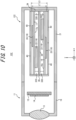
- the first convex support portion 320 and the second convex support portion 330 may be integrally formed with the first shield portion 35, or may be formed by members different from a member of the first shield portion 35 and fixed to the first shield portion 35. In the example illustrated in FIG. 10 , the first convex support portion 320 and the second convex support portion 330 are formed by members different from the member of the first shield portion 35.
- Each of the second shield portions 36 has a second wall portion 39 and two bottom surfaces 40.
- the second wall portion 39 is, for example, a plate-like member.
- the second wall portion 39 has a rectangular shape.
- a longitudinal length L1 (in the z-direction in FIG. 11 ) of the second wall portion 39 is equal to or longer than a distance L2 between the two first wall portions 37 fixed to the connection portion 38.
- a transverse length L3 (in the y-direction in FIG. 11 ) of the second wall portion 39 is equal to a length L4 of the first wall portion 37 extending in the direction (the y-direction in FIG. 11 ) orthogonal to the longitudinal direction of the first wall portion 37.
- the second wall portion 39 may have heat conductivity.
- the second wall portions 39 may have electrical conductivity.
- the second wall portions 39 may be formed from a metal material.
- the bottom surface 40 is, for example, a plate-like member.
- the bottom surface 40 has a rectangular shape.
- the two bottom surfaces 40 can improve the electromagnetic compatibility of the electronic components 19 arranged in the vicinity of the bottom surfaces 40.
- the two bottom surfaces 40 are vertically provided on the longitudinal sides of the second wall portions 39 in a manner perpendicular to the plate surface of the second wall portions 39.
- a sum of lengths L51 and L52 in the direction (in the x-direction in FIG. 11 ) normal to the surface of the second wall portion 39 is equal to or longer than a length L6 of the longitudinal direction of the first wall portion 37 (in the x-direction in FIG. 11 ).
- the bottom surfaces 40 may have electrical conductivity.
- the bottom surfaces 400 may be formed from a metal material.
- the first shield portion 35 is fitted into the space between the two bottom surfaces 40 of the second shield portion 36.
- the first shield portion 35 is fitted into the second shield portion 36 in such a manner that the two first wall portions 37 are perpendicular to the second wall portions 39 and the bottom surfaces 40.
- the first shield portion 35 is fitted into each of the two second shield portions 36 in such a manner that the second wall portions 39 of the two second shield portions 36 oppose each other.
- the two first wall portions 37 and the second wall portions 39 together form an enclosure portion that has a rectangular tube shape framing a rectangular flat plate and surrounds the electronic components 19.
- the length L3 between the two bottom surfaces 40 is longer than a length L7 in the axial direction of a structure formed when the electronic components 19 are mounted on each of the first circuit board 17 and the second circuit board 18 fixed to the first shield portion 35.
- the third electronic component 24 is surrounded by one of the bottom surfaces 40 of each of the two shield portions 36, the first wall portions 37, and the second wall portions 39.
- the fourth electronic component 25 is surrounded by the other one of the bottom surfaces 40 of each of the two second shield portions 36, the first wall portions 37, and the second wall portions 39.
- the second electronic apparatus 122 at least one of the electronic components 19 is provided on at least one of the first opposing surface 17a and the second opposing surface 18a, in the same manner as the first embodiment. Also, the enclosure portion 20 formed by the first wall portions 37 and the second wall portions 39 contacts the second housing 21 and, simultaneously, encloses a space that includes one or more electronic components 19 within the space between the first circuit board 17 and the second circuit board 18.
- the second electronic apparatus 122 can improve the heat dissipation effectiveness for heat generated by the electronic components 19. Further, the second electronic apparatus 122 can improve the heat dissipation effectiveness with a smaller number of elements than that of a case in which a heat absorbing member is provided for each of the electronic components 19 mounted on the two circuit boards.
- an imaging apparatus 103 according to the fifth embodiment of the present disclosure will be described.
- the fifth embodiment will be described below, focusing on its features which differ from those of the fourth embodiment. Components having the same configurations as those of the fourth embodiment are denoted by the same reference numerals.
- the imaging apparatus 103 includes the first electronic apparatus 11 and a second electronic apparatus (an electronic apparatus) 123.
- the first electronic apparatus 11 has the same configuration and function as those of the fourth embodiment.
- the second electronic apparatus 123 includes the first circuit board 17, the second circuit board 18, one or more electronic components 19, the second housing 21, a first convex support portion 320, and a second convex support portion 330.
- the configurations and functions of the first circuit board 17, the second circuit board 18, the electronic components 19, the second housing 21, the first convex support portion 320, and the second convex support portion 330 of the second electronic apparatus 123 are the same as those of the fourth embodiment.
- the second electronic apparatus 123 further includes a first shield portion 350 and a second shield portion 360.
- the first shield portion 350 has two first wall portions 37 and a connection portion 38.
- the first shield portion 350 also has a third wall portion 41.
- the functions and structures of the two first wall portions 37 and the connection portion 38 are the same as those of the fourth embodiment.
- the third wall portion 41 is, for example, a plate-like member.
- the third wall portion 41 has a rectangular shape.
- the third wall portion 41 is vertically fixed to one end surface in the longitudinal direction (the x-direction in FIG. 13 ) of each of the two first wall portions 37.
- the third wall portion 41 may have heat conductivity.
- the third wall portion 41 may have electrical conductivity.
- the third wall portion 41 may be formed from a metal material.
- the second shield portion 360 has the second wall portion 39 and two bottom surfaces 400.
- the second wall portion 39 has the same configuration and function as those of the fourth embodiment.
- Each of the bottom surfaces 400 is a rectangular plate-like member.
- each of the bottom surfaces 400 has a rectangular shape.
- the two bottom surfaces 400 are provided vertical to the longitudinal sides of the second wall portion 39.
- a length L8 of the bottom surface 400 normal to the second wall portion 39 (in the x-direction in FIG. 13 ) is equal to or longer than the length L6 in the longitudinal direction (in the x-direction in FIG. 13 ) of the first wall portion 37.
- the bottom surfaces 400 may have electrical conductivity.
- each of the bottom surfaces 400 may be formed from a metal material.
- the first shield portion 350 is fitted into the space between the two bottom surfaces 400 of the second shield portion 360.
- the two first wall portions 37 are perpendicular to each of the second wall portion 39 and the bottom surfaces 400, and the first shield portion 350 is fitted into the second shielding portion 36 in such a manner that the third wall portion 41 opposes the second wall portion 39.
- the first wall portions 37, the second wall portion 39, and the third wall portion 41 together form an enclosure portion that has a rectangular tube shape that frames a rectangular flat plate and surrounds the electronic components 19.
- the second electronic apparatus 123 at least one of the electronic components 19 is provided on at least one of the first opposing surface 17a and the second opposing surface 18a, in the same manner as the first embodiment. Also, the enclosure portion formed by the first wall portions 37, the second wall portion 39, and the third wall portion 41 contacts the second housing 21 and, simultaneously, encloses the space that includes one or more electronic components 19 within the space between the first circuit board 17 and the second circuit board 18.
- the second electronic apparatus 123 can improve the heat dissipation effectiveness for heat generated by the electronic component 19. Further, the second electronic apparatus 123 can improve the heat dissipation effectiveness with a smaller number of elements than that of a case in which a heat absorbing member is provided for each of the electronic components 19 mounted on the two circuit boards.
- an imaging apparatus 104 according to a sixth embodiment of the present disclosure will be described.
- the sixth embodiment will be described below, focusing on its features which differ from those of the first embodiment. Components having the same configurations as those of the first embodiment are denoted by the same reference numerals.
- the imaging apparatus 104 includes the first electronic apparatus 11 and a second electronic apparatus (an electronic apparatus) 124.
- the first electronic apparatus 11 has the same configuration and function as those of the first embodiment.
- the second electronic apparatus 124 includes the first circuit board 17, the second circuit board 18, one or more electronic components 19, the enclosure portion 20, and the second housing 21.
- the configurations and functions of the first circuit board 17, the second circuit board 18, the electronic components 19, the enclosure portion 20, and the second housing 21 of the second electronic apparatus 124 are the same as those of the first embodiment.
- the second electronic apparatus 124 further includes a heat conductor 42.
- the heat conductor 42 is fixed in a manner so as to contact at least one of the first electronic component 22 and the second electronic component 23.
- the heat conductor 42 is fixed in a manner so as to contact the enclosure portion 20.
- the heat conductor 42 is, for example, a plate-like member. In particular, the heat conductor 42 has a rectangular shape.
- the heat conductor 42 is arranged in parallel with the first circuit board 17 and the second circuit board 18.
- the heat conductor 42 may be integrally formed with the enclosure portion 20.
- the partition wall 31 may be formed by a member different from a member of the enclosure portion 20 and fixed to the enclosure portion 20. In the example illustrated in FIG. 10 , the heat conductor 42 is formed by a member different from the member of the enclosure portion 20.
- the second electronic apparatus 124 at least one of the electronic components 19 is provided on at least one of the first opposing surface 17a and the second opposing surface 18a, in the same manner as the first embodiment. Also, the enclosure portion 20 contacts the second housing 21 and, simultaneously, encloses the space that includes one or more electronic components 19 within the space between the first circuit board 17 and the second circuit board 18.
- the second electronic apparatus 124 can improve the heat dissipation effectiveness for heat generated by the electronic components 19. Further, the second electronic apparatus 124 can improve the heat dissipation effectiveness with a smaller number of elements than that of a case in which a heat absorbing member is provided for each of the electronic components 19 mounted on the two circuit boards.
- the second electronic apparatus 124 includes the first electronic component 22, the second electronic component 23, and the heat conductor 42 that contacts the enclosure portion 20.
- the heat conductor 42 efficiently conducts heat generated by the first electronic component 22 to the enclosure portion 20. Accordingly, the second electronic apparatus 124 can efficiently conduct heat generated by the first electronic component 22 to the second housing 21 for dissipation via the heat conductor 42.
Landscapes
- Engineering & Computer Science (AREA)
- Microelectronics & Electronic Packaging (AREA)
- Physics & Mathematics (AREA)
- Multimedia (AREA)
- Signal Processing (AREA)
- Thermal Sciences (AREA)
- General Physics & Mathematics (AREA)
- Aviation & Aerospace Engineering (AREA)
- Electromagnetism (AREA)
- Cooling Or The Like Of Electrical Apparatus (AREA)
- Shielding Devices Or Components To Electric Or Magnetic Fields (AREA)
- Cameras Adapted For Combination With Other Photographic Or Optical Apparatuses (AREA)
- Camera Bodies And Camera Details Or Accessories (AREA)
- Studio Devices (AREA)
- Telephone Set Structure (AREA)
- Mounting Of Printed Circuit Boards And The Like (AREA)
Abstract
Description
- This application claims priority to
Japanese Patent Application No. 2018-060744 filed on March 27, 2018 - The present disclosure relates to an electronic apparatus, an imaging apparatus, and a mobile body.
- It is conventionally known to provide a heat absorbing member on an electronic component in order to release heat generated by the electronic component mounted on a circuit board (e.g., PTL 1).
- PTL 1:
JP 2014-036066 A - An electronic apparatus according to an embodiment of the present disclosure includes a first circuit board, a second circuit board, one or more electronic components, an enclosure portion, and a housing. The one or more electronic components are mounted on at least one of opposing surfaces of the first circuit board and the second circuit board that oppose each other. The enclosure portion supports a surface of each of the first circuit board and the second circuit board to oppose each other with a predetermined gap therebetween. The enclosure portion encloses a gap space that includes the one or more electronic components within a space between the first circuit board and the second circuit board. The housing accommodates the first circuit board, the second circuit board, and the enclosure portion. The enclosure portion contacts the housing.
- An imaging apparatus according to an embodiment of the present disclosure includes an electronic apparatus. The electronic apparatus includes a first circuit board, a second circuit board, one or more electronic components, an enclosure portion, and a housing. The one or more electronic components are mounted on at least one of opposing surfaces of the first circuit board and the second circuit board that oppose each other. The enclosure portion supports a surface of each of the first circuit board and the second circuit board to oppose each other with a predetermined gap therebetween. The enclosure portion encloses a gap space that includes the one or more electronic components within a space between the first circuit board and the second circuit board. The housing accommodates the first circuit board, the second circuit board, and the enclosure portion. The enclosure portion contacts the housing.
- A mobile body according to an embodiment of the present disclosure includes an electronic apparatus. The electronic apparatus includes a first circuit board, a second circuit board, one or more electronic components, an enclosure portion, and a housing. The one or more electronic components are mounted on at least one of opposing surfaces of the first circuit board and the second circuit board that oppose each other. The enclosure portion supports a surface of each of the first circuit board and the second circuit board to oppose each other with a predetermined gap therebetween. The enclosure portion encloses a gap space that includes the one or more electronic components within a space between the first circuit board and the second circuit board. The housing accommodates the first circuit board, the second circuit board, and the enclosure portion. The enclosure portion contacts the housing.
-
-
FIG. 1 is a schematic diagram illustrating a mobile body equipped with an imaging apparatus that includes an electronic apparatus illustrated inFIG. 1 ; -
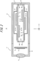
FIG. 2 is a cross-sectional view illustrating an imaging apparatus that includes an electronic apparatus according to a first embodiment; -
FIG. 3 is a perspective view illustrating an enclosure portion illustrated inFIG. 2 ; -
FIG. 4 is an exploded perspective view illustrating an example of the electronic apparatus illustrated inFIG. 2 ; -
FIG. 5 is an exploded perspective view illustrating another example of the electronic apparatus illustrated inFIG. 2 ; -
FIG. 6 is a cross-sectional view illustrating an imaging apparatus that includes an electronic apparatus according to a second embodiment; -
FIG. 7 is a perspective view illustrating an enclosure portion and a partition wall illustrated inFIG. 6 ; -
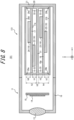
FIG. 8 is a cross-sectional view illustrating an imaging apparatus that includes an electronic apparatus according to a third embodiment; -
FIG. 9 is a perspective view illustrating an enclosure portion, a partition wall, and first convex support portions illustrated inFIG. 8 ; -
FIG. 10 is a cross-sectional view illustrating an imaging apparatus that includes an electronic apparatus according to a fourth embodiment; -
FIG. 11 is an exploded perspective view illustrating a portion of an electronic apparatus that includes a portion illustrated inFIG. 10 ; -
FIG. 12 is a cross-sectional view illustrating an imaging apparatus that includes an electronic apparatus according to a fifth embodiment; -
FIG. 13 is an exploded perspective view illustrating a portion of an electronic apparatus that includes a portion illustrated inFIG. 12 ; and -
FIG. 14 is a cross-sectional diagram illustrating an imaging apparatus that includes an electronic apparatus according to a sixth embodiment. - With the increased performance of apparatuses having electronic components mounted therein, it is necessary for apparatuses to house a plurality of substrates having respective electronic components mounted thereon. However, providing a heat absorbing member to each of the electronic components mounted on the plurality of substrates increases the number of elements and hinders miniaturization of the apparatuses.
- The present disclosure aims to provide an electronic apparatus, an imaging apparatus, and a mobile body that can be downsized while maintaining effective heat dissipation.
- Hereinafter, an
imaging apparatus 10 according to a first embodiment of the present disclosure will be described with reference to the drawings. - As illustrated in
FIG. 1 , theimaging apparatus 10 may be mounted on amobile body 50 in a manner so as to be able to image a scene surrounding themobile body 50. Themobile body 50 may encompass, for example, vehicles, ships, and aircrafts. Vehicles may include, for example, automobiles, industrial vehicles, rail vehicles, domestic vehicles, and fixed-wing aircrafts that travel on a runway. Automobiles may include, for example, cars, trucks, buses, motorcycles, and trolley buses. Industrial vehicles may include, for example, agricultural vehicles and construction vehicles. Industrial vehicles may include, for example, forklifts and golf carts. Industrial vehicles for agricultural purpose may include, for example, tractors, tillers, transplanters, binders, combined harvesters, and lawn mowers. Industrial vehicles for construction purpose may include, for example, bulldozers, scrapers, excavators, crane trucks, dump trucks, and load rollers. Vehicles may include human-powered vehicles that travel on human power. Classification of the vehicles is not limited to the above. For example, vehicles may include industrial vehicles authorized to travel on the road. A plurality of categories may include the same type of vehicles. Vessels may include, for example, watercraft, boats, and tankers. Aircraft may include, for example, fixed wing aircraft and rotorcraft. - As illustrated in
FIG. 2 , theimaging apparatus 10 includes a firstelectronic apparatus 11 and a second electronic apparatus (electronic apparatus) 12. In the following description, an optical axis direction of a lens, which will be described later, will be referred to as an x-direction, a normal direction of afirst circuit board 17 and asecond circuit board 18, which will be described later, will be referred to as a y-direction, and a direction perpendicular to the x-direction and the y-direction will be referred to as an x-direction. - The first
electronic apparatus 11 includes an imagingoptical system 13, animage sensor 14, animage sensor substrate 15, and afirst housing 16. - The imaging
optical system 13 includes one or more lenses. The imagingoptical system 13 is fixed to thefirst housing 16 such that an optical axis OX of the imagingoptical system 13 is perpendicular to an imaging surface of theimage sensor 14. The imagingoptical system 13 forms light incident from a subject as a subject image on the imaging surface of theimage sensor 14. - The
image sensor 14 generates an image including the subject image formed on the imaging surface by the imagingoptical system 13. Theimage sensor 14 is, for example, a CMOS (Complementary Metal Oxide Semiconductor) image sensor or a CCD (Charge Coupled Device). Theimage sensor 14 is mounted on theimage sensor substrate 15. - The
image sensor substrate 15 is a plate-like member. Theimage sensor substrate 15 has theimage sensor 14 and the like mounted thereon. - The
first housing 16 houses the imagingoptical system 13 and theimage sensor substrate 15 having theimage sensor 14 mounted thereon. - The second
electronic apparatus 12 performs image processing on the image generated by the firstelectronic apparatus 11. The secondelectronic apparatus 12 may send a signal to the firstelectronic apparatus 11, based on the image processing. The secondelectronic apparatus 12 includes afirst circuit board 17, asecond circuit board 18,electronic components 19, anenclosure portion 20, and a second housing (housing) 21. The secondelectronic apparatus 12 may further include afirst shield portion 26 and asecond shield portion 27. - The
first circuit board 17 and thesecond circuit board 18 are plate-like members. Thefirst circuit board 17 and thesecond circuit board 18 are arranged such that respective surfaces of each oppose each other in parallel. - The
electronic components 19 are components constituting an electronic circuit. Theelectronic component 19 include, for example, resistors, capacitors, diodes, or an integrated circuit including these elements. - The
electronic components 19 include at least one of a firstelectronic component 22 and a secondelectronic component 23. Theelectronic components 19 may include a thirdelectronic component 24 and a fourthelectronic component 25. At least one of theelectronic components 19 is mounted on at least one of a first opposingsurface 17a and a second opposingsurface 18a, which will be described later. The firstelectronic component 22 is mounted on the first opposingsurface 17a of thefirst circuit board 17. The secondelectronic component 23 is mounted on the second opposingsurface 18a of thesecond circuit board 18. The firstelectronic component 22 and the secondelectronic component 23 are arranged within the secondelectronic apparatus 12 in a manner so as to not interfere with each other. - The third
electronic component 24 may be mounted on a surface of thefirst circuit board 17 which is opposite from the first opposingsurface 17a. The fourthelectronic component 25 may be mounted on a surface of thesecond circuit board 18 which is opposite from the second opposingsurface 18a. - The
enclosure portion 20 supports thefirst circuit board 17 and thesecond circuit board 18 such that one surface of thefirst circuit board 17 and one surface of thesecond circuit board 18 oppose each other with a predetermined gap therebetween. Theenclosure portion 20 encloses a space that includes the firstelectronic component 22 and the secondelectronic component 23 within a space between thefirst circuit board 17 and thesecond circuit board 18. - The
enclosure portion 20 is, for example, a tubular member as illustrated inFIG. 3 . In particular, theenclosure portion 20 has a rectangular tube shape that frames a rectangular flat plate. Theenclosure portion 20 may be formed by a single member in which a plurality of flat plates are integrally formed. Theenclosure portion 20 may be formed by a member in which a plurality of members are fixed to one another. In the present embodiment, theenclosure portion 20 is formed by a single member. - As illustrated in
FIG. 2 , theenclosure portion 20 fixes thefirst circuit board 17 and thesecond circuit board 18 at end portions thereof in an axial direction (the y-direction inFIG. 2 ). For example, theenclosure portion 20 fixes peripheral edge portions of the first opposingsurface 17a of thefirst circuit board 17 atend surfaces 20a arranged in the axial direction (the y-direction inFIG. 2 ) of the rectangular tube. The first opposingsurface 17a is a surface of thefirst circuit board 17 that opposes thesecond circuit board 18. Theenclosure portion 20 is fixed to peripheral edge portions of the second opposingsurface 18a of thesecond circuit board 18 at end surfaces 20b arranged in the axial direction (the y-direction inFIG. 2 ) of the rectangular tube. The second opposingsurface 18a is a surface of thesecond circuit board 18 that opposes thefirst circuit board 17. - The
enclosure portion 20 fixes thefirst circuit board 17 and thesecond circuit board 18 via an adhesive, soldering, a screw, or the like. As a result, theenclosure portion 20 supports thefirst circuit board 17 and thesecond circuit board 18 with a predetermined gap therebetween. The predetermined gap corresponds to an axial length of theenclosure portion 20. - The
enclosure portion 20 may have heat conductivity. Theenclosure portion 20 may have electrical conductivity. For example, theenclosure portion 20 may be formed from a metal material. Theenclosure portion 20 may be grounded to the ground of at least one of thefirst circuit board 17 and thesecond circuit board 18. - The
first shield portion 26 can improve the electromagnetic compatibility (EMC) of the thirdelectronic component 24. Thefirst shield portion 26 shields the thirdelectronic component 24 and can be fixed to thefirst circuit board 17. Thesecond shield portion 27 can improve the electromagnetic compatibility of the fourthelectronic component 25. Thesecond shield portion 27 shields the fourthelectronic component 25 and can be fixed to thesecond circuit board 18. Each of thefirst shield portion 26 and thesecond shield portion 27 is formed from a conductive material. - The
second housing 21 houses thefirst circuit board 17 having the firstelectronic component 22 mounted thereon, thesecond circuit board 18 having the secondelectronic component 23 mounted thereon, and theenclosure portion 20 supporting thefirst circuit board 17 and thesecond circuit board 18. Thesecond housing 21 contacts at least a part of theenclosure portion 20 and fixes theenclosure portion 20 housed within thesecond housing 21. Thesecond housing 21 may have a fitting structure to fix theenclosure portion 20. - In one example as illustrated in
FIG. 4 , thesecond housing 21 includesguide portions 28 provided on theinner wall surface 21a. Theenclosure portion 20 has external surfaces provided withfitting portions 29 to be fitted into theguide portions 28. In a manufacturing process, when theenclosure portion 20 supporting thefirst circuit board 17 and thesecond circuit board 18 as described above is inserted into thesecond housing 21, thefitting portions 29 are guided by theguide portions 28, and thus theenclosure portion 20 is housed within thesecond housing 21. - In another example as illustrated in
FIG. 5 , thesecond housing 21 has openingwalls 21b formed in thesecond housing 21. Theenclosure portion 20 hasprotrusions 30 to be fitted intoopenings 21c defined by the openingwalls 21b. In the manufacturing process, when theenclosure portion 20 supporting thefirst circuit board 17 and thesecond circuit board 18 as described above is inserted into thesecond housing 21, theprotrusions 30 are fitted into theopenings 21c, and thus theenclosure portion 20 is housed within thesecond housing 21. - According to the first embodiment, as described above, at least one of the
electronic components 19 is mounted on at least one of the first opposingsurface 17a and the second opposingsurface 18a. Also, theenclosure portion 20 contacts thesecond housing 21 and, simultaneously, encloses a space that includes one or more of theelectronic components 19 within the space between thefirst circuit board 17 and thesecond circuit board 18. In the secondelectronic apparatus 12, thus, theenclosure portion 20 can absorb heat generated by theelectronic components 19 and dissipate the heat to the outside via thesecond housing 21. As a result, the secondelectronic apparatus 12 can improve the heat dissipation effectiveness for heat generated by theelectronic components 19. Further, because the secondelectronic apparatus 12 requires fewer components than a case in which respective heat absorbing members are provided to theelectronic components 19 mounted on the two circuit boards, the secondelectronic apparatus 12 can be miniaturized. - According to the first embodiment, in the second
electronic apparatus 12 theenclosure portion 20 has electrical conductivity and is grounded to the ground of at least one of thefirst circuit board 17 and thesecond circuit board 18. In the secondelectronic apparatus 12, thus, theenclosure portion 20 can improve the electromagnetic compatibility of theelectronic components 19. - According to the first embodiment, also, in the second
electronic apparatus 12 the thirdelectronic component 24 is mounted on the surface of thefirst circuit board 17 which is opposite from the first opposingsurface 17a. In the secondelectronic apparatus 12, further, thefirst shield portion 26 that can be fixed to theenclosure portion 20 shields the thirdelectronic component 24. As a result, the secondelectronic apparatus 12 can allow mounting of moreelectronic components 19 without increasing the number of circuit boards and further reduce leakage of electromagnetic waves generated by theelectronic components 19. Thus, the secondelectronic apparatus 12 can improve electromagnetic wave suppression effectiveness and suppress a size increase thereof while allowing the mounting of manyelectronic components 19. - Next, an
imaging apparatus 100 according to a second embodiment of the present disclosure will be described. The second embodiment will be described below, focusing on its features which differ from those of the first embodiment. Components having the same configurations as those of the first embodiment are denoted by the same reference numerals. - As illustrated in
FIG. 6 , theimaging apparatus 100 includes the firstelectronic apparatus 11 and a second electronic apparatus (electronic apparatus) 120. The firstelectronic apparatus 11 has the same structure and function as those of the first embodiment. - The second
electronic apparatus 120 includes thefirst circuit board 17, thesecond circuit board 18,electronic components 19, theenclosure portion 20, and thesecond housing 21. The structures and functions of thefirst circuit board 17, thesecond circuit board 18, theelectronic components 19, theenclosure portion 20, and thesecond housing 21 of the secondelectronic apparatus 120 are the same as those of the first embodiment. The secondelectronic apparatus 120 further includes apartition wall 31. - As illustrated in
FIG. 7 , thepartition wall 31 is, for example, a plate-like member. In particular, thepartition wall 31 has a rectangular shape. As illustrated inFIG. 6 , thepartition wall 31 partitions a space between thefirst circuit board 17 and thesecond circuit board 18 into a space that includes the firstelectronic component 22 and a space that includes the secondelectronic component 23. Thepartition wall 31 may be formed by a single member that is integrally formed with theenclosure portion 20. Thepartition wall 31 may be configured to be a member separate from theenclosure portion 20 and fixed to theenclosure portion 20. - In particular, the
partition wall 31 is integrally formed with theenclosure portion 20 at any portion between both ends in the axial direction of theenclosure portion 20, as illustrated inFIG. 6 andFIG. 7 . Although in the example illustrated inFIG. 6 thepartition wall 31 is integrally formed at a portion including a midpoint of theend surface 20a and theend surface 20b, this is not restrictive. Thepartition wall 31 may be integrally formed at any portion between both ends of theenclosure portion 20. - The
partition wall 31 may have heat conductivity. Thepartition wall 31 may have electrical conductivity. For example, thepartition wall 31 may be formed from a metal material. Thepartition wall 31 may directly contact at least one of the firstelectronic component 22 and the secondelectronic component 23. Also, thepartition wall 31 may indirectly contact at least one of the firstelectronic component 22 and the secondelectronic component 23 via aheat conductor 34. - According to the second embodiment, as described above, in the second
electronic apparatus 120 at least one of theelectronic components 19 is provided on at least one of the first opposingsurface 17a and the second opposingsurface 18a, in the same manner as the first embodiment. In the secondelectronic apparatus 120, also, theenclosure portion 20 contacts thesecond housing 21 and, simultaneously, encloses the space that includes one or more of theelectronic components 19 within the space between thefirst circuit board 17 and thesecond circuit board 18. Thus, the secondelectronic apparatus 120 can improve heat dissipation effectiveness for heat generated by theelectronic components 19. Further, the secondelectronic apparatus 120 can improve the heat dissipation effectiveness with fewer elements than that of a case in which a heat absorbing member is provided for each of theelectronic components 19 mounted on the two circuit boards. - According to the second embodiment, in the second
electronic apparatus 120 thepartition wall 31 partitions the space between thefirst circuit board 17 and thesecond circuit board 18 into the space that includes the firstelectronic component 22 and the space that includes the secondelectronic component 23. Thus, in the secondelectronic apparatus 120 thepartition wall 31 can suppress the conduction of heat generated by the firstelectronic component 22 to the secondelectronic component 23 and enable heat dissipation to the outside of thesecond housing 21 via theenclosure portion 20. In the secondelectronic apparatus 120, also, thepartition wall 31 can suppress the conduction of heat generated by the secondelectronic component 23 to the firstelectronic component 22 and enable heat dissipation to the outside of thesecond housing 21 via theenclosure portion 20. As a result, the secondelectronic apparatus 120 can further improve the heat dissipation effectiveness. In the secondelectronic apparatus 120, further, thepartition wall 31 shields both electromagnetic waves that are generated by the firstelectronic component 22 and propagate towards the secondelectronic component 23 and electromagnetic waves that are generated by the secondelectronic component 23 and propagate towards the firstelectronic component 22. Accordingly, the secondelectronic apparatus 120 can improve electromagnetic compatibility of each of the firstelectronic component 22 and the secondelectronic component 23. - According to the second embodiment, in the second
electronic apparatus 120 thepartition wall 31 directly or indirectly contacts the firstelectronic component 22. In the secondelectronic apparatus 120, thus, thepartition wall 31 conducts the heat generated from the firstelectronic component 22 to thesecond housing 21 in contact with thepartition wall 31, for heat dissipation. Thus, the secondelectronic apparatus 120 can more efficiently conduct heat to thesecond housing 21 than a case in which the firstelectronic component 22 does not contact thepartition wall 31, and thus improve the heat dissipation effect. - According to the second embodiment, the second
electronic apparatus 120 further includes theheat conductors 34 in contact with thepartition wall 31 and theelectronic components 19. The firstelectronic component 22 and the secondelectronic component 23 may not necessarily contact thepartition wall 31. On the other hand, in the secondelectronic apparatus 120 having the configuration described above, at least one of the firstelectronic component 22 and the secondelectronic component 23 that may not necessarily come into direct contact with thepartition wall 31 contacts thepartition wall 31 via theheat conductor 34. In the secondelectronic apparatus 120, thus, theheat conductors 34 can efficiently conduct heat generated from at least one of the firstelectronic component 22 and the secondelectronic component 23 via thepartition wall 31. Accordingly, the secondelectronic apparatus 120 can efficiently dissipate heat generated by at least one of the firstelectronic component 22 and the secondelectronic component 23. - Next, an
imaging apparatus 101 according to a third embodiment of the present disclosure will be described. The third embodiment will be described below, focusing on its features which differ from those of the first embodiment. Components having the same configurations as those of the first embodiment are denoted by the same reference numerals. - As illustrated in
FIG. 8 , theimaging apparatus 101 includes the firstelectronic apparatus 11 and a second electronic apparatus (electronic apparatus) 121. The firstelectronic apparatus 11 has the same configuration and function as those of the first embodiment. - The second
electronic apparatus 121 includes thefirst circuit board 17, thesecond circuit board 18, one or moreelectronic components 19, theenclosure portion 20, and thesecond housing 21. The structures and functions of thefirst circuit board 17, thesecond circuit board 18, theelectronic components 19, theenclosure portion 20, and thesecond housing 21 of the secondelectronic apparatus 121 are the same as those of the first embodiment. The secondelectronic apparatus 121 further includes firstconvex support portions 32 and secondconvex support portions 33. The secondelectronic apparatus 121 may further include afirst shield portion 260, asecond shield portion 270, and thepartition wall 31. Thepartition wall 31 is the same as that of the second embodiment. - As illustrated in
FIG. 9 , the firstconvex support portions 32 are arranged in the space enclosed by theenclosure portion 20. The firstconvex support portions 32 are arranged on one side of thepartition wall 31. Each of the firstconvex support portions 32 may be formed by a single member integrally formed with thepartition wall 31. Thepartition wall 31 may be configured as a member separate from theenclosure portion 20 and fixed to theenclosure portion 20. - The second
electronic apparatus 121 has three firstconvex support portions 32. In this configuration, the three firstconvex support portions 32 are arranged in such a manner that one of them deviates from a straight line connecting the other two of the firstconvex support portions 32. For example, the firstconvex support portions 32 is arranged at each of two adjacent corners of a rectangle enclosed by theenclosure portion 20 and a position on a side opposite from a side located between the two adjacent corners. Each of the three firstconvex support portions 32 has a flat surface on its side for supporting thefirst circuit board 17. Each of the three firstconvex support portions 32 fixes thefirst circuit board 17 on the flat surface. In this way, the three firstconvex support portions 32 support thefirst circuit board 17 within a plane including end portions of the three firstconvex support portions 32. - The second
electronic apparatus 121 may include one firstconvex support portion 32. In a configuration in which the secondelectronic apparatus 121 includes one firstconvex support portion 32, the firstconvex support portion 32 has a plane perpendicular to the axial direction (the y-direction inFIG. 9 ) of theenclosure portion 20. The firstconvex support portion 32 supports thefirst circuit board 17 by fixing it to the plane. The number of the firstconvex support portions 32 included in the secondelectronic apparatus 121 may be two, four, or more. - As illustrated in
FIG. 8 , an axial height h1 of the firstconvex support portion 32 is less than a height h2 from thepartition wall 31 to theend surface 20a in the axial direction of theenclosure portion 20. - The second
convex support portions 33 have a function and a configuration that are similar to those of the firstconvex support portion 32. The secondconvex support portions 33 are different from the firstconvex support portions 32, in terms of being arranged on the surface of thepartition wall 31 on the opposite side from the surface on which the firstconvex support portion 32 is arranged. A height h3 in the axial direction of the firstconvex support portion 32 is lower than a height h4 from thepartition wall 31 to theaxial end surface 20a of theenclosure portion 20, in a manner similar to the firstconvex support portion 32. - In this configuration, the first
convex support portion 32 and the secondconvex support portion 33 support thefirst circuit board 17 and thesecond circuit board 18 with a predetermined gap therebetween, in such a manner that one surface of thefirst circuit board 17 and one surface of thesecond circuit board 18 oppose each other. The predetermined gap is a sum of the height h1 of the firstconvex support portion 32, the height h3 of the secondconvex support portion 33, and a thickness h5 of thepartition wall 31. - The
first shield portion 260 and thesecond shield portion 270 can improve the electromagnetic compatibility of the thirdelectronic component 24 and the fourthelectronic component 25, respectively, in a manner similar to the first embodiment. Thefirst shield portion 260 can be fixed to theend surface 20a of theenclosure portion 20. Thesecond shield portion 270 can be fixed to theend surface 20b of theenclosure portion 20. Thefirst shield portion 260 and thesecond shield portion 270 are, for example, plate-like members. In particular, each of thefirst shield portion 260 and thesecond shield portion 270 has a rectangular shape. In a configuration in which a height h6 of theenclosure portion 20 from the surface not opposing thepartition wall 31 of thefirst circuit board 17 to theend surface 20a in the axial direction is higher than an axial height of the thirdelectronic component 24, thefirst shield portion 260 can shield the thirdelectronic component 24. In a configuration in which a height h7 of theenclosure portion 20 from the surface not opposing thepartition wall 31 of thesecond circuit board 18 to theend surface 20b in the axial direction is higher than an axial height of the fourthelectronic component 25, thesecond shield portion 270 can shield the fourthelectronic component 25. - According to the third embodiment, as described above, in the second
electronic apparatus 121 at least one of theelectronic components 19 is provided on at least one of the first opposingsurface 17a and the second opposingsurface 18a, in a manner the same as the first embodiment. In the secondelectronic apparatus 121, also, theenclosure portion 20 contacts thesecond housing 21 and, simultaneously, encloses a space that includes one or moreelectronic components 19 in the space between thefirst circuit board 17 and thesecond circuit board 18. Thus, the secondelectronic apparatus 121 can improve the heat dissipation effectiveness for heat radiated from theelectronic component 19. Further, the secondelectronic apparatus 121 can improve the heat dissipation effectiveness with a smaller number of elements than that of a case in which a heat absorbing member is provided for each of theelectronic components 19 mounted on the two circuit boards. - Next, an
imaging apparatus 102 according to a fourth embodiment of the present disclosure will be described. The fourth embodiment will be described below, focusing on its features which differ from those of the first embodiment. Components having the same configurations as those of the first embodiment are denoted by the same reference numerals. - As illustrated in
FIG. 10 , theimaging apparatus 102 includes the firstelectronic apparatus 11 and a second electronic apparatus (electronic apparatus) 122. The firstelectronic apparatus 11 has the same configuration and function as that of the first embodiment. - The second
electronic apparatus 122 includes thefirst circuit board 17, thesecond circuit board 18, one or moreelectronic components 19, and thesecond housing 21. The configurations and functions of thefirst circuit board 17, thesecond circuit board 18, theelectronic components 19, and thesecond housing 21 of the secondelectronic apparatus 122 are the same as those of the first embodiment. The secondelectronic apparatus 122 further includes afirst shield portion 35, twosecond shield portions 36, a firstconvex support portion 320, and a secondconvex support portion 330. - As illustrated in
FIG. 11 , thefirst shield portion 35 has twofirst wall portions 37 and aconnection portion 38. - Each of the
first wall portions 37 is, for example, a plate-like member. In particular, each of thefirst wall portions 37 has a rectangular shape. A longitudinal length (in the x-direction inFIG. 11 ) of each of thefirst wall portions 37 is equal to or longer than a length of a first side of each of the surfaces of thefirst circuit board 17 and thesecond circuit board 18. Thefirst wall portions 37 may have heat conductivity. Thefirst wall portions 37 may have electrical conductivity. For example, thefirst wall portions 37 may be formed from a metal material. - The
connection portion 38 supports the twofirst wall portions 37 with a predetermined gap therebetween. Theconnection portion 38 supports the twofirst wall portions 37 such that they are in parallel with each other. The predetermined gap is equal to or longer than a length of a second side orthogonal to the first side of each of the surfaces of thefirst circuit board 17 and thesecond circuit board 18. Theconnection portion 38 is, for example, a plate-like member. In particular, theconnection portion 38 has a rectangular shape. Thepartition wall 31 of the second embodiment may be adopted as theconnection portion 38. Although in the example illustrated inFIG. 11 theconnection portion 38 fixes each of the twofirst wall portions 37 substantially over the entire longitudinal direction of the twofirst wall portions 37, theconnection portion 38 may fix thefirst wall portions 37 in potions thereof. - The first
convex support portion 320 and the secondconvex support portion 330 are arranged in a space enclosed by thefirst wall portions 37 and thesecond wall portion 39, which will be described later. The firstconvex support portion 320 and the secondconvex support portion 330 have the same functions and structures as those of the third embodiment. The firstconvex support portion 320 and the secondconvex support portion 330 may be integrally formed with thefirst shield portion 35, or may be formed by members different from a member of thefirst shield portion 35 and fixed to thefirst shield portion 35. In the example illustrated inFIG. 10 , the firstconvex support portion 320 and the secondconvex support portion 330 are formed by members different from the member of thefirst shield portion 35. - Each of the
second shield portions 36 has asecond wall portion 39 and two bottom surfaces 40. - The
second wall portion 39 is, for example, a plate-like member. In particular, thesecond wall portion 39 has a rectangular shape. A longitudinal length L1 (in the z-direction inFIG. 11 ) of thesecond wall portion 39 is equal to or longer than a distance L2 between the twofirst wall portions 37 fixed to theconnection portion 38. A transverse length L3 (in the y-direction inFIG. 11 ) of thesecond wall portion 39 is equal to a length L4 of thefirst wall portion 37 extending in the direction (the y-direction inFIG. 11 ) orthogonal to the longitudinal direction of thefirst wall portion 37. Thesecond wall portion 39 may have heat conductivity. Thesecond wall portions 39 may have electrical conductivity. For example, thesecond wall portions 39 may be formed from a metal material. - The
bottom surface 40 is, for example, a plate-like member. In particular, thebottom surface 40 has a rectangular shape. The twobottom surfaces 40 can improve the electromagnetic compatibility of theelectronic components 19 arranged in the vicinity of the bottom surfaces 40. The twobottom surfaces 40 are vertically provided on the longitudinal sides of thesecond wall portions 39 in a manner perpendicular to the plate surface of thesecond wall portions 39. In each of the bottom surfaces 40 of the twosecond shield portions 35, a sum of lengths L51 and L52 in the direction (in the x-direction inFIG. 11 ) normal to the surface of thesecond wall portion 39 is equal to or longer than a length L6 of the longitudinal direction of the first wall portion 37 (in the x-direction inFIG. 11 ). The bottom surfaces 40 may have electrical conductivity. For example, the bottom surfaces 400 may be formed from a metal material. - The
first shield portion 35 is fitted into the space between the twobottom surfaces 40 of thesecond shield portion 36. Thefirst shield portion 35 is fitted into thesecond shield portion 36 in such a manner that the twofirst wall portions 37 are perpendicular to thesecond wall portions 39 and the bottom surfaces 40. Thefirst shield portion 35 is fitted into each of the twosecond shield portions 36 in such a manner that thesecond wall portions 39 of the twosecond shield portions 36 oppose each other. - In a state in which the
first shield portion 35 is fitted into the twosecond shield portions 36, the twofirst wall portions 37 and thesecond wall portions 39 together form an enclosure portion that has a rectangular tube shape framing a rectangular flat plate and surrounds theelectronic components 19. - As illustrated in
FIG. 10 , the length L3 between the twobottom surfaces 40 is longer than a length L7 in the axial direction of a structure formed when theelectronic components 19 are mounted on each of thefirst circuit board 17 and thesecond circuit board 18 fixed to thefirst shield portion 35. The thirdelectronic component 24 is surrounded by one of the bottom surfaces 40 of each of the twoshield portions 36, thefirst wall portions 37, and thesecond wall portions 39. Similarly, the fourthelectronic component 25 is surrounded by the other one of the bottom surfaces 40 of each of the twosecond shield portions 36, thefirst wall portions 37, and thesecond wall portions 39. - According to the fourth embodiment, as described above, in the second
electronic apparatus 122 at least one of theelectronic components 19 is provided on at least one of the first opposingsurface 17a and the second opposingsurface 18a, in the same manner as the first embodiment. Also, theenclosure portion 20 formed by thefirst wall portions 37 and thesecond wall portions 39 contacts thesecond housing 21 and, simultaneously, encloses a space that includes one or moreelectronic components 19 within the space between thefirst circuit board 17 and thesecond circuit board 18. Thus, the secondelectronic apparatus 122 can improve the heat dissipation effectiveness for heat generated by theelectronic components 19. Further, the secondelectronic apparatus 122 can improve the heat dissipation effectiveness with a smaller number of elements than that of a case in which a heat absorbing member is provided for each of theelectronic components 19 mounted on the two circuit boards. - Next, an
imaging apparatus 103 according to the fifth embodiment of the present disclosure will be described. The fifth embodiment will be described below, focusing on its features which differ from those of the fourth embodiment. Components having the same configurations as those of the fourth embodiment are denoted by the same reference numerals. - As illustrated in
FIG. 12 , theimaging apparatus 103 includes the firstelectronic apparatus 11 and a second electronic apparatus (an electronic apparatus) 123. The firstelectronic apparatus 11 has the same configuration and function as those of the fourth embodiment. - The second
electronic apparatus 123 includes thefirst circuit board 17, thesecond circuit board 18, one or moreelectronic components 19, thesecond housing 21, a firstconvex support portion 320, and a secondconvex support portion 330. The configurations and functions of thefirst circuit board 17, thesecond circuit board 18, theelectronic components 19, thesecond housing 21, the firstconvex support portion 320, and the secondconvex support portion 330 of the secondelectronic apparatus 123 are the same as those of the fourth embodiment. The secondelectronic apparatus 123 further includes afirst shield portion 350 and asecond shield portion 360. - As illustrated in
FIG. 13 , thefirst shield portion 350 has twofirst wall portions 37 and aconnection portion 38. Thefirst shield portion 350 also has athird wall portion 41. The functions and structures of the twofirst wall portions 37 and theconnection portion 38 are the same as those of the fourth embodiment. - The
third wall portion 41 is, for example, a plate-like member. In particular, thethird wall portion 41 has a rectangular shape. Thethird wall portion 41 is vertically fixed to one end surface in the longitudinal direction (the x-direction inFIG. 13 ) of each of the twofirst wall portions 37. Thethird wall portion 41 may have heat conductivity. Thethird wall portion 41 may have electrical conductivity. For example, thethird wall portion 41 may be formed from a metal material. - The
second shield portion 360 has thesecond wall portion 39 and twobottom surfaces 400. Thesecond wall portion 39 has the same configuration and function as those of the fourth embodiment. - Each of the bottom surfaces 400 is a rectangular plate-like member. In particular, each of the bottom surfaces 400 has a rectangular shape. The two
bottom surfaces 400 are provided vertical to the longitudinal sides of thesecond wall portion 39. A length L8 of thebottom surface 400 normal to the second wall portion 39 (in the x-direction inFIG. 13 ) is equal to or longer than the length L6 in the longitudinal direction (in the x-direction inFIG. 13 ) of thefirst wall portion 37. The bottom surfaces 400 may have electrical conductivity. For example, each of the bottom surfaces 400 may be formed from a metal material. - The
first shield portion 350 is fitted into the space between the twobottom surfaces 400 of thesecond shield portion 360. In thefirst shield portion 350, the twofirst wall portions 37 are perpendicular to each of thesecond wall portion 39 and the bottom surfaces 400, and thefirst shield portion 350 is fitted into thesecond shielding portion 36 in such a manner that thethird wall portion 41 opposes thesecond wall portion 39. - In a state in which the
first shield portion 350 is fitted in thesecond shield portion 360, thefirst wall portions 37, thesecond wall portion 39, and thethird wall portion 41 together form an enclosure portion that has a rectangular tube shape that frames a rectangular flat plate and surrounds theelectronic components 19. - According to the fifth embodiment, as described above, in the second
electronic apparatus 123 at least one of theelectronic components 19 is provided on at least one of the first opposingsurface 17a and the second opposingsurface 18a, in the same manner as the first embodiment. Also, the enclosure portion formed by thefirst wall portions 37, thesecond wall portion 39, and thethird wall portion 41 contacts thesecond housing 21 and, simultaneously, encloses the space that includes one or moreelectronic components 19 within the space between thefirst circuit board 17 and thesecond circuit board 18. Thus, the secondelectronic apparatus 123 can improve the heat dissipation effectiveness for heat generated by theelectronic component 19. Further, the secondelectronic apparatus 123 can improve the heat dissipation effectiveness with a smaller number of elements than that of a case in which a heat absorbing member is provided for each of theelectronic components 19 mounted on the two circuit boards. - Next, an
imaging apparatus 104 according to a sixth embodiment of the present disclosure will be described. The sixth embodiment will be described below, focusing on its features which differ from those of the first embodiment. Components having the same configurations as those of the first embodiment are denoted by the same reference numerals. - As illustrated in
FIG. 14 , theimaging apparatus 104 includes the firstelectronic apparatus 11 and a second electronic apparatus (an electronic apparatus) 124. The firstelectronic apparatus 11 has the same configuration and function as those of the first embodiment. - The second
electronic apparatus 124 includes thefirst circuit board 17, thesecond circuit board 18, one or moreelectronic components 19, theenclosure portion 20, and thesecond housing 21. The configurations and functions of thefirst circuit board 17, thesecond circuit board 18, theelectronic components 19, theenclosure portion 20, and thesecond housing 21 of the secondelectronic apparatus 124 are the same as those of the first embodiment. The secondelectronic apparatus 124 further includes aheat conductor 42. - The
heat conductor 42 is fixed in a manner so as to contact at least one of the firstelectronic component 22 and the secondelectronic component 23. Theheat conductor 42 is fixed in a manner so as to contact theenclosure portion 20. Theheat conductor 42 is, for example, a plate-like member. In particular, theheat conductor 42 has a rectangular shape. Theheat conductor 42 is arranged in parallel with thefirst circuit board 17 and thesecond circuit board 18. Theheat conductor 42 may be integrally formed with theenclosure portion 20. Thepartition wall 31 may be formed by a member different from a member of theenclosure portion 20 and fixed to theenclosure portion 20. In the example illustrated inFIG. 10 , theheat conductor 42 is formed by a member different from the member of theenclosure portion 20. - According to the sixth embodiment, as described above, in the second
electronic apparatus 124 at least one of theelectronic components 19 is provided on at least one of the first opposingsurface 17a and the second opposingsurface 18a, in the same manner as the first embodiment. Also, theenclosure portion 20 contacts thesecond housing 21 and, simultaneously, encloses the space that includes one or moreelectronic components 19 within the space between thefirst circuit board 17 and thesecond circuit board 18. Thus, the secondelectronic apparatus 124 can improve the heat dissipation effectiveness for heat generated by theelectronic components 19. Further, the secondelectronic apparatus 124 can improve the heat dissipation effectiveness with a smaller number of elements than that of a case in which a heat absorbing member is provided for each of theelectronic components 19 mounted on the two circuit boards. - According to the sixth embodiment, the second
electronic apparatus 124 includes the firstelectronic component 22, the secondelectronic component 23, and theheat conductor 42 that contacts theenclosure portion 20. In the secondelectronic apparatus 124, thus, theheat conductor 42 efficiently conducts heat generated by the firstelectronic component 22 to theenclosure portion 20. Accordingly, the secondelectronic apparatus 124 can efficiently conduct heat generated by the firstelectronic component 22 to thesecond housing 21 for dissipation via theheat conductor 42. - Although the above embodiments have been described as representative examples, it will be apparent to those skilled in the art that numerous modifications and substitutions can be made within the spirit and scope of the present disclosure. Accordingly, the present disclosure should not be construed as being limited by the embodiments described above, and various modifications and changes can be made without departing from the scope of the claims. For example, a plurality of constituent blocks described in the embodiments and examples can be combined, or one constituent block can be subdivided.
- The drawings explaining the embodiments described above according to the present disclosure are for illustrative purpose only and are not necessarily drawn to scale.
- In the following, further embodiments 1 to 10 of the present invention are described.
- 1. An electronic apparatus comprising:
- a first circuit board and a second circuit board;
- one or more electronic components mounted on at least one of opposing surfaces of the first circuit board and the second circuit board that oppose each other;
- an enclosure portion configured to support a surface of each of the first circuit board and the second circuit board to oppose each other with a predetermined gap therebetween and to enclose a gap space that includes the one or more electronic components, within a space between the first circuit board and the second circuit board; and
- a housing configured to accommodate the first circuit board, the second circuit board, and the enclosure portion, the enclosure portion contacting the housing.
- 2. The electronic apparatus according to embodiment 1,
wherein the enclosure portion has heat conductivity and electrical conductivity and is grounded to a ground of at least one of the first circuit board and the second circuit board. - 3. The electronic apparatus according to
embodiment 1 or 2,- wherein the one or more electronic components include a first electronic component mounted on the first circuit board and a second electronic component mounted on the second circuit board, and
- the first electronic component and the second electronic component are arranged in a space defined by the predetermined gap, in a manner so as to not interfere with each other.
- 4. The electronic apparatus according to any one of embodiments 1 to 3, further comprising a partition wall that is fixed to the enclosure portion and partitions a space between the first circuit board and the second circuit board into a space that includes an electronic component of the one or more electronic components that is mounted on the first circuit board and a space that includes an electronic component of the one or more electronic components that is mounted on the second circuit board.
- 5. The electronic apparatus according to embodiment 4,
wherein the partition wall directly or indirectly contacts the one or more electronic components. - 6. The electronic apparatus according to embodiment 5,
further comprising a heat conductor that contacts the partition wall and one of the one or more electronic components. - 7. The electronic apparatus according to any one of embodiments 1 to 3, further comprising a heat conductor that contacts an electronic component mounted on the first circuit board, an electronic component mounted on the second circuit board, and a partition wall.
- 8. The electronic apparatus according to any one of embodiments 1 to 7, further comprising:
- another electronic component mounted on at least one surface on an opposite side of the opposing surfaces of the first circuit board and the second circuit board; and
- a shielding portion that shields the electronic component and fixable to the enclosure portion.
- 9. An imaging apparatus comprising:
an electronic apparatus that includes:- a first circuit board and a second circuit board;
- one or more electronic components mounted on at least one of opposing surfaces of the first circuit board and the second circuit board that oppose each other;
- an enclosure portion configured to support a surface of each of the first circuit board and the second circuit board to oppose each other with a predetermined gap therebetween and to enclose a gap space that includes the one or more electronic components, within a space between the first circuit board and the second circuit board; and
- a housing configured to accommodate the first circuit board, the second circuit board, and the enclosure portion, the enclosure portion contacting the housing.
- 10. A mobile body comprising:
an electronic apparatus that includes:- a first circuit board and a second circuit board;
- one or more electronic components mounted on at least one of opposing surfaces of the first circuit board and the second circuit board that oppose each other;
- an enclosure portion configured to support a surface of each of the first circuit board and the second circuit board to oppose each other with a predetermined gap therebetween and to enclose a gap space that includes the one or more electronic components, within a space between the first circuit board and the second circuit board; and
- a housing configured to accommodate the first circuit board, the second circuit board, and the enclosure portion, the enclosure portion contacting the housing.
-
- 10, 100, 101, 102, 103, 104
- imaging apparatus
- 11
- first electronic apparatus
- 12, 120, 121, 122, 123, 124
- second electronic apparatus (electronic apparatus)
- 13
- imaging optical system
- 14
- image sensor
- 15
- image sensor substrate
- 16
- first housing
- 17
- first circuit board
- 17a
- first opposing surface
- 18
- second circuit board
- 18a
- second opposing surface
- 19
- electronic component
- 20
- enclosure portion
- 20a, 20b
- end surface
- 21
- second housing (housing)
- 21a
- inner wall surface
- 21b
- opening wall
- 21c
- opening
- 22
- first electronic component
- 23
- second electronic component
- 24
- third electronic component
- 25
- fourth electronic component
- 26
- first shield portion
- 27
- second shield portion
- 28
- guide portion
- 29
- fitting portion
- 30
- protrusion
- 31
- partition wall
- 32, 320
- first convex support portion
- 33, 330
- second convex support portion
- 34, 42
- heat conductor
- 35, 350
- first shield portion
- 36, 360
- second shield portion
- 37
- first wall portion
- 38
- connection portion
- 39
- second wall portion
- 40, 400
- bottom portion
- 41
- third wall portion
- 50
- mobile body
Claims (8)
- An electronic apparatus comprising:a first circuit board and a second circuit board;one or more electronic components mounted on at least one of opposing surfaces of the first circuit board and the second circuit board that oppose each other;an enclosure portion configured to support a surface of each of the first circuit board and the second circuit board to oppose each other with a predetermined gap therebetween, to enclose a gap space that includes the one or more electronic components, within a space between the first circuit board and the second circuit board and to have heat conductivity;a partition wall configured to contact the enclosure portion, to partition a space between the first circuit board and the second circuit board and to directly or indirectly contact the one or more electronic components; anda housing configured to accommodate the enclosure portion, the enclosure portion contacting the housing.
- The electronic apparatus according to claim 1,
wherein the enclosure portion has electrical conductivity and is grounded to a ground of at least one of the first circuit board and the second circuit board. - The electronic apparatus according to claim 1 or 2,wherein the one or more electronic components include a first electronic component mounted on the first circuit board and a second electronic component mounted on the second circuit board, andthe first electronic component and the second electronic component are arranged in a space defined by the predetermined gap, in a manner so as to not interfere with each other.
- The electronic apparatus according to any one of claims 1 to 3,
further comprising a heat conductor that contacts the partition wall and one of the one or more electronic components. - The electronic apparatus according to any one of claims 1 to 4,
further comprising a heat conductor that contacts an electronic component mounted on the first circuit board, an electronic component mounted on the second circuit board, and a partition wall. - The electronic apparatus according to any one of claims 1 to 5, further comprising:another electronic component mounted on at least one surface on an opposite side of the opposing surfaces of the first circuit board and the second circuit board; anda shielding portion that shields the electronic component and fixable to the enclosure portion.
- An imaging apparatus comprising:
an electronic apparatus that includes:a first circuit board and a second circuit board;one or more electronic components mounted on at least one of opposing surfaces of the first circuit board and the second circuit board that oppose each other;an enclosure portion configured to support a surface of each of the first circuit board and the second circuit board to oppose each other with a predetermined gap therebetween, to enclose a gap space that includes the one or more electronic components, within a space between the first circuit board and the second circuit board and to have heat conductivity;a partition wall configured to contact the enclosure portion, to partition a space between the first circuit board and the second circuit board and to directly or indirectly contact the one or more electronic components; anda housing configured to accommodate the enclosure portion, the enclosure portion contacting the housing. - A mobile body comprising:
an electronic apparatus that includes:a first circuit board and a second circuit board;one or more electronic components mounted on at least one of opposing surfaces of the first circuit board and the second circuit board that oppose each other;an enclosure portion configured to support a surface of each of the first circuit board and the second circuit board to oppose each other with a predetermined gap therebetween, to enclose a gap space that includes the one or more electronic components, within a space between the first circuit board and the second circuit board and to have heat conductivity;a partition wall configured to contact the enclosure portion, to partition a space between the first circuit board and the second circuit board and to directly or indirectly contact the one or more electronic components; anda housing configured to accommodate the enclosure portion, the enclosure portion contacting the housing.
Applications Claiming Priority (3)
| Application Number | Priority Date | Filing Date | Title |
|---|---|---|---|
| JP2018060744A JP7158163B2 (en) | 2018-03-27 | 2018-03-27 | Electronic devices, imaging devices, and mobile objects |
| PCT/JP2019/010309 WO2019188300A1 (en) | 2018-03-27 | 2019-03-13 | Electronic equipment, imaging device, and mobile body |
| EP19774962.5A EP3780922B1 (en) | 2018-03-27 | 2019-03-13 | Electronic equipment, imaging device, and mobile body |
Related Parent Applications (2)
| Application Number | Title | Priority Date | Filing Date |
|---|---|---|---|
| EP19774962.5A Division EP3780922B1 (en) | 2018-03-27 | 2019-03-13 | Electronic equipment, imaging device, and mobile body |
| EP19774962.5A Division-Into EP3780922B1 (en) | 2018-03-27 | 2019-03-13 | Electronic equipment, imaging device, and mobile body |
Publications (2)
| Publication Number | Publication Date |
|---|---|
| EP4236337A2 true EP4236337A2 (en) | 2023-08-30 |
| EP4236337A3 EP4236337A3 (en) | 2023-10-11 |
Family
ID=68058857
Family Applications (2)
| Application Number | Title | Priority Date | Filing Date |
|---|---|---|---|
| EP23181996.2A Withdrawn EP4236337A3 (en) | 2018-03-27 | 2019-03-13 | Electronic equipment, imaging device, and mobile body |
| EP19774962.5A Active EP3780922B1 (en) | 2018-03-27 | 2019-03-13 | Electronic equipment, imaging device, and mobile body |
Family Applications After (1)
| Application Number | Title | Priority Date | Filing Date |
|---|---|---|---|
| EP19774962.5A Active EP3780922B1 (en) | 2018-03-27 | 2019-03-13 | Electronic equipment, imaging device, and mobile body |
Country Status (5)
| Country | Link |
|---|---|
| US (1) | US11382230B2 (en) |
| EP (2) | EP4236337A3 (en) |
| JP (1) | JP7158163B2 (en) |
| CN (2) | CN111869340B (en) |
| WO (1) | WO2019188300A1 (en) |
Families Citing this family (5)
| Publication number | Priority date | Publication date | Assignee | Title |
|---|---|---|---|---|
| JP7322523B2 (en) * | 2019-06-06 | 2023-08-08 | オムロン株式会社 | Electronics |
| JP2022181350A (en) * | 2021-05-26 | 2022-12-08 | シャープ株式会社 | Electronic component |
| DE102021116319A1 (en) * | 2021-06-24 | 2022-12-29 | Valeo Schalter Und Sensoren Gmbh | CAMERA DEVICE FOR A VEHICLE, VEHICLE AND METHOD OF MANUFACTURING A CAMERA DEVICE |
| DE112022007360T5 (en) * | 2022-08-31 | 2025-04-03 | Hitachi Astemo, Ltd. | ELECTRONIC CONTROL DEVICE |
| EP4637289A1 (en) * | 2024-04-19 | 2025-10-22 | Aptiv Technologies AG | Emc assembly |
Family Cites Families (25)
| Publication number | Priority date | Publication date | Assignee | Title |
|---|---|---|---|---|
| US5586388A (en) * | 1991-05-31 | 1996-12-24 | Nippondenso Co., Ltd. | Method for producing multi-board electronic device |
| JPH0745982A (en) * | 1993-07-28 | 1995-02-14 | Toshiba Corp | Connection structure between shield case and printed wiring board |
| US5581443A (en) * | 1994-09-14 | 1996-12-03 | Kabushiki Kaisha Toshiba | Structure for cooling a circuit module having a circuit board and a heat-generating IC chip mounted on the board, and portable electronic apparatus incorporating the structure |
| JP2692619B2 (en) * | 1994-11-24 | 1997-12-17 | 日本電気株式会社 | Wireless transceiver |
| JP2000196266A (en) * | 1998-12-24 | 2000-07-14 | Furukawa Electric Co Ltd:The | Heating electronic component storage unit |
| JP2000294972A (en) * | 1999-04-05 | 2000-10-20 | Sharp Corp | Shielding device for mounting board |
| JP2008140924A (en) * | 2006-11-30 | 2008-06-19 | Toshiba Corp | Electronics |
| JP2008227258A (en) * | 2007-03-14 | 2008-09-25 | Yazaki Corp | Circuit board heat dissipation structure and electrical junction box having the same |
| JP2009117409A (en) * | 2007-11-01 | 2009-05-28 | Siix Corp | Circuit board |
| US9986175B2 (en) | 2009-03-02 | 2018-05-29 | Flir Systems, Inc. | Device attachment with infrared imaging sensor |
| JP4938055B2 (en) * | 2009-07-10 | 2012-05-23 | シャープ株式会社 | Tuner unit and flat-screen TV receiver |
| JP2011054640A (en) * | 2009-08-31 | 2011-03-17 | Funai Electric Co Ltd | Shield package substrate |
| JP2011170566A (en) * | 2010-02-17 | 2011-09-01 | Toshiba Corp | Semiconductor storage device and electronic device |
| JP5165012B2 (en) * | 2010-02-22 | 2013-03-21 | 三菱電機株式会社 | Resin-sealed electronic control device and manufacturing method thereof |
| JP2014036066A (en) * | 2012-08-08 | 2014-02-24 | Sharp Corp | Shield case having heat radiation effect and circuit unit including the same |
| WO2015025687A1 (en) * | 2013-08-19 | 2015-02-26 | 株式会社日立国際電気 | Electronic device |
| JP2015170618A (en) * | 2014-03-04 | 2015-09-28 | 株式会社東芝 | Electronic apparatus |
| KR101785368B1 (en) * | 2014-04-23 | 2017-10-16 | 엘지이노텍 주식회사 | Camera module for Vehicle |
| EP3163864B1 (en) * | 2014-06-26 | 2019-11-06 | Kyocera Corporation | Image-capturing device and vehicle |
| KR102248086B1 (en) * | 2014-11-14 | 2021-05-04 | 엘지이노텍 주식회사 | Camera module using for automobile |
| JP6320332B2 (en) * | 2015-03-10 | 2018-05-09 | 東芝メモリ株式会社 | Electronics |
| JP6850080B2 (en) * | 2016-05-27 | 2021-03-31 | 株式会社キーエンス | Image processing sensor |
| JP6884553B2 (en) * | 2016-11-04 | 2021-06-09 | エドワーズ株式会社 | Assembling method of vacuum pump control device, vacuum pump, and vacuum pump control device |
| JP2018133846A (en) * | 2017-02-13 | 2018-08-23 | 矢崎総業株式会社 | Battery monitoring device |
| JP7141877B2 (en) * | 2018-07-18 | 2022-09-26 | キオクシア株式会社 | semiconductor storage device |
-
2018
- 2018-03-27 JP JP2018060744A patent/JP7158163B2/en active Active
-
2019
- 2019-03-13 CN CN201980020347.3A patent/CN111869340B/en active Active
- 2019-03-13 EP EP23181996.2A patent/EP4236337A3/en not_active Withdrawn
- 2019-03-13 WO PCT/JP2019/010309 patent/WO2019188300A1/en not_active Ceased
- 2019-03-13 US US17/041,617 patent/US11382230B2/en active Active
- 2019-03-13 EP EP19774962.5A patent/EP3780922B1/en active Active
- 2019-03-13 CN CN202311022095.2A patent/CN116866697A/en active Pending
Also Published As
| Publication number | Publication date |
|---|---|
| JP2019175949A (en) | 2019-10-10 |
| CN116866697A (en) | 2023-10-10 |
| WO2019188300A1 (en) | 2019-10-03 |
| EP3780922A4 (en) | 2021-12-01 |
| EP3780922A1 (en) | 2021-02-17 |
| EP4236337A3 (en) | 2023-10-11 |
| EP3780922B1 (en) | 2023-08-23 |
| CN111869340B (en) | 2023-09-05 |
| JP7158163B2 (en) | 2022-10-21 |
| US11382230B2 (en) | 2022-07-05 |
| CN111869340A (en) | 2020-10-30 |
| US20210014994A1 (en) | 2021-01-14 |
Similar Documents
| Publication | Publication Date | Title |
|---|---|---|
| US11382230B2 (en) | Electronic apparatus, imaging apparatus, and mobile body | |
| CN113589618B (en) | Device for fixing camera module circuit board and camera module | |
| EP3392689B1 (en) | Imaging device component, and imaging device | |
| CN109845239B (en) | Camera module | |
| JP7328398B2 (en) | Electronic devices, imaging devices, and mobile objects | |
| TW201841433A (en) | Pluggable module with cooling channel | |
| JP7189073B2 (en) | Electronic device, imaging device, moving body, and imaging device manufacturing method | |
| US12127330B2 (en) | Electronic control device | |
| JP7303361B2 (en) | Imaging device | |
| EP2985990B1 (en) | Stereo camera device | |
| CN113632446B (en) | Electronic equipment, camera devices, and moving objects | |
| JP7224514B2 (en) | Electronic devices, imaging devices, and mobile objects | |
| JP2018082028A (en) | Electric power unit | |
| WO2024166265A1 (en) | Electronic control device | |
| JP2025129841A (en) | In-vehicle cameras | |
| HK40069315A (en) | Sensor device | |
| JP6380247B2 (en) | Electronic device casing and image sensor using the same | |
| JP2021197435A (en) | Optical transmission module and electronic control device |
Legal Events
| Date | Code | Title | Description |
|---|---|---|---|
| PUAI | Public reference made under article 153(3) epc to a published international application that has entered the european phase |
Free format text: ORIGINAL CODE: 0009012 |
|
| STAA | Information on the status of an ep patent application or granted ep patent |
Free format text: STATUS: THE APPLICATION HAS BEEN PUBLISHED |
|
| AC | Divisional application: reference to earlier application |
Ref document number: 3780922 Country of ref document: EP Kind code of ref document: P |
|
| AK | Designated contracting states |
Kind code of ref document: A2 Designated state(s): AL AT BE BG CH CY CZ DE DK EE ES FI FR GB GR HR HU IE IS IT LI LT LU LV MC MK MT NL NO PL PT RO RS SE SI SK SM TR |
|
| REG | Reference to a national code |
Ref country code: DE Ref legal event code: R079 Free format text: PREVIOUS MAIN CLASS: H04N0023520000 Ipc: G03B0017550000 |
|
| PUAL | Search report despatched |
Free format text: ORIGINAL CODE: 0009013 |
|
| AK | Designated contracting states |
Kind code of ref document: A3 Designated state(s): AL AT BE BG CH CY CZ DE DK EE ES FI FR GB GR HR HU IE IS IT LI LT LU LV MC MK MT NL NO PL PT RO RS SE SI SK SM TR |
|
| RIC1 | Information provided on ipc code assigned before grant |
Ipc: H04N 23/52 20230101ALI20230906BHEP Ipc: H04N 23/51 20230101ALI20230906BHEP Ipc: G03B 17/55 20210101AFI20230906BHEP |
|
| STAA | Information on the status of an ep patent application or granted ep patent |
Free format text: STATUS: THE APPLICATION IS DEEMED TO BE WITHDRAWN |
|
| 18D | Application deemed to be withdrawn |
Effective date: 20240412 |