EP4235768A2 - Integrated structures with antenna elements and ic chips employing edge contact connections - Google Patents
Integrated structures with antenna elements and ic chips employing edge contact connections Download PDFInfo
- Publication number
- EP4235768A2 EP4235768A2 EP23174399.8A EP23174399A EP4235768A2 EP 4235768 A2 EP4235768 A2 EP 4235768A2 EP 23174399 A EP23174399 A EP 23174399A EP 4235768 A2 EP4235768 A2 EP 4235768A2
- Authority
- EP
- European Patent Office
- Prior art keywords
- chip
- cavity
- substrate
- edge contact
- sidewall
- Prior art date
- Legal status (The legal status is an assumption and is not a legal conclusion. Google has not performed a legal analysis and makes no representation as to the accuracy of the status listed.)
- Granted
Links
Images





Classifications
-
- H—ELECTRICITY
- H01—ELECTRIC ELEMENTS
- H01Q—ANTENNAS, i.e. RADIO AERIALS
- H01Q1/00—Details of, or arrangements associated with, antennas
- H01Q1/12—Supports; Mounting means
- H01Q1/22—Supports; Mounting means by structural association with other equipment or articles
- H01Q1/2283—Supports; Mounting means by structural association with other equipment or articles mounted in or on the surface of a semiconductor substrate as a chip-type antenna or integrated with other components into an IC package
-
- H—ELECTRICITY
- H01—ELECTRIC ELEMENTS
- H01Q—ANTENNAS, i.e. RADIO AERIALS
- H01Q1/00—Details of, or arrangements associated with, antennas
- H01Q1/36—Structural form of radiating elements, e.g. cone, spiral, umbrella; Particular materials used therewith
- H01Q1/38—Structural form of radiating elements, e.g. cone, spiral, umbrella; Particular materials used therewith formed by a conductive layer on an insulating support
-
- H—ELECTRICITY
- H01—ELECTRIC ELEMENTS
- H01Q—ANTENNAS, i.e. RADIO AERIALS
- H01Q21/00—Antenna arrays or systems
- H01Q21/0087—Apparatus or processes specially adapted for manufacturing antenna arrays
- H01Q21/0093—Monolithic arrays
-
- H—ELECTRICITY
- H10—SEMICONDUCTOR DEVICES; ELECTRIC SOLID-STATE DEVICES NOT OTHERWISE PROVIDED FOR
- H10W—GENERIC PACKAGES, INTERCONNECTIONS, CONNECTORS OR OTHER CONSTRUCTIONAL DETAILS OF DEVICES COVERED BY CLASS H10
- H10W44/00—Electrical arrangements for controlling or matching impedance
- H10W44/20—Electrical arrangements for controlling or matching impedance at high-frequency [HF] or radio frequency [RF]
-
- H—ELECTRICITY
- H10—SEMICONDUCTOR DEVICES; ELECTRIC SOLID-STATE DEVICES NOT OTHERWISE PROVIDED FOR
- H10W—GENERIC PACKAGES, INTERCONNECTIONS, CONNECTORS OR OTHER CONSTRUCTIONAL DETAILS OF DEVICES COVERED BY CLASS H10
- H10W70/00—Package substrates; Interposers; Redistribution layers [RDL]
- H10W70/01—Manufacture or treatment
- H10W70/05—Manufacture or treatment of insulating or insulated package substrates, or of interposers, or of redistribution layers
- H10W70/093—Connecting or disconnecting other interconnections thereto or therefrom, e.g. connecting bond wires or bumps
-
- H—ELECTRICITY
- H10—SEMICONDUCTOR DEVICES; ELECTRIC SOLID-STATE DEVICES NOT OTHERWISE PROVIDED FOR
- H10W—GENERIC PACKAGES, INTERCONNECTIONS, CONNECTORS OR OTHER CONSTRUCTIONAL DETAILS OF DEVICES COVERED BY CLASS H10
- H10W70/00—Package substrates; Interposers; Redistribution layers [RDL]
- H10W70/01—Manufacture or treatment
- H10W70/05—Manufacture or treatment of insulating or insulated package substrates, or of interposers, or of redistribution layers
- H10W70/095—Manufacture or treatment of insulating or insulated package substrates, or of interposers, or of redistribution layers of vias therein
-
- H—ELECTRICITY
- H10—SEMICONDUCTOR DEVICES; ELECTRIC SOLID-STATE DEVICES NOT OTHERWISE PROVIDED FOR
- H10W—GENERIC PACKAGES, INTERCONNECTIONS, CONNECTORS OR OTHER CONSTRUCTIONAL DETAILS OF DEVICES COVERED BY CLASS H10
- H10W70/00—Package substrates; Interposers; Redistribution layers [RDL]
- H10W70/60—Insulating or insulated package substrates; Interposers; Redistribution layers
- H10W70/611—Insulating or insulated package substrates; Interposers; Redistribution layers for connecting multiple chips together
-
- H—ELECTRICITY
- H10—SEMICONDUCTOR DEVICES; ELECTRIC SOLID-STATE DEVICES NOT OTHERWISE PROVIDED FOR
- H10W—GENERIC PACKAGES, INTERCONNECTIONS, CONNECTORS OR OTHER CONSTRUCTIONAL DETAILS OF DEVICES COVERED BY CLASS H10
- H10W70/00—Package substrates; Interposers; Redistribution layers [RDL]
- H10W70/60—Insulating or insulated package substrates; Interposers; Redistribution layers
- H10W70/62—Insulating or insulated package substrates; Interposers; Redistribution layers characterised by their interconnections
- H10W70/63—Vias, e.g. via plugs
- H10W70/635—Through-vias
-
- H—ELECTRICITY
- H10—SEMICONDUCTOR DEVICES; ELECTRIC SOLID-STATE DEVICES NOT OTHERWISE PROVIDED FOR
- H10W—GENERIC PACKAGES, INTERCONNECTIONS, CONNECTORS OR OTHER CONSTRUCTIONAL DETAILS OF DEVICES COVERED BY CLASS H10
- H10W70/00—Package substrates; Interposers; Redistribution layers [RDL]
- H10W70/60—Insulating or insulated package substrates; Interposers; Redistribution layers
- H10W70/67—Insulating or insulated package substrates; Interposers; Redistribution layers characterised by their insulating layers or insulating parts
- H10W70/68—Shapes or dispositions thereof
-
- H—ELECTRICITY
- H10—SEMICONDUCTOR DEVICES; ELECTRIC SOLID-STATE DEVICES NOT OTHERWISE PROVIDED FOR
- H10W—GENERIC PACKAGES, INTERCONNECTIONS, CONNECTORS OR OTHER CONSTRUCTIONAL DETAILS OF DEVICES COVERED BY CLASS H10
- H10W70/00—Package substrates; Interposers; Redistribution layers [RDL]
- H10W70/60—Insulating or insulated package substrates; Interposers; Redistribution layers
- H10W70/67—Insulating or insulated package substrates; Interposers; Redistribution layers characterised by their insulating layers or insulating parts
- H10W70/68—Shapes or dispositions thereof
- H10W70/681—Shapes or dispositions thereof comprising holes not having chips therein, e.g. for outgassing, underfilling or bond wire passage
-
- H—ELECTRICITY
- H10—SEMICONDUCTOR DEVICES; ELECTRIC SOLID-STATE DEVICES NOT OTHERWISE PROVIDED FOR
- H10W—GENERIC PACKAGES, INTERCONNECTIONS, CONNECTORS OR OTHER CONSTRUCTIONAL DETAILS OF DEVICES COVERED BY CLASS H10
- H10W70/00—Package substrates; Interposers; Redistribution layers [RDL]
- H10W70/60—Insulating or insulated package substrates; Interposers; Redistribution layers
- H10W70/67—Insulating or insulated package substrates; Interposers; Redistribution layers characterised by their insulating layers or insulating parts
- H10W70/68—Shapes or dispositions thereof
- H10W70/685—Shapes or dispositions thereof comprising multiple insulating layers
-
- H—ELECTRICITY
- H10—SEMICONDUCTOR DEVICES; ELECTRIC SOLID-STATE DEVICES NOT OTHERWISE PROVIDED FOR
- H10W—GENERIC PACKAGES, INTERCONNECTIONS, CONNECTORS OR OTHER CONSTRUCTIONAL DETAILS OF DEVICES COVERED BY CLASS H10
- H10W72/00—Interconnections or connectors in packages
- H10W72/20—Bump connectors, e.g. solder bumps or copper pillars; Dummy bumps; Thermal bumps
-
- H—ELECTRICITY
- H10—SEMICONDUCTOR DEVICES; ELECTRIC SOLID-STATE DEVICES NOT OTHERWISE PROVIDED FOR
- H10W—GENERIC PACKAGES, INTERCONNECTIONS, CONNECTORS OR OTHER CONSTRUCTIONAL DETAILS OF DEVICES COVERED BY CLASS H10
- H10W72/00—Interconnections or connectors in packages
- H10W72/90—Bond pads, in general
-
- H—ELECTRICITY
- H10—SEMICONDUCTOR DEVICES; ELECTRIC SOLID-STATE DEVICES NOT OTHERWISE PROVIDED FOR
- H10W—GENERIC PACKAGES, INTERCONNECTIONS, CONNECTORS OR OTHER CONSTRUCTIONAL DETAILS OF DEVICES COVERED BY CLASS H10
- H10W90/00—Package configurations
-
- H—ELECTRICITY
- H10—SEMICONDUCTOR DEVICES; ELECTRIC SOLID-STATE DEVICES NOT OTHERWISE PROVIDED FOR
- H10W—GENERIC PACKAGES, INTERCONNECTIONS, CONNECTORS OR OTHER CONSTRUCTIONAL DETAILS OF DEVICES COVERED BY CLASS H10
- H10W90/00—Package configurations
- H10W90/701—Package configurations characterised by the relative positions of pads or connectors relative to package parts
-
- H—ELECTRICITY
- H10—SEMICONDUCTOR DEVICES; ELECTRIC SOLID-STATE DEVICES NOT OTHERWISE PROVIDED FOR
- H10W—GENERIC PACKAGES, INTERCONNECTIONS, CONNECTORS OR OTHER CONSTRUCTIONAL DETAILS OF DEVICES COVERED BY CLASS H10
- H10W95/00—Packaging processes not covered by the other groups of this subclass
-
- H—ELECTRICITY
- H10—SEMICONDUCTOR DEVICES; ELECTRIC SOLID-STATE DEVICES NOT OTHERWISE PROVIDED FOR
- H10W—GENERIC PACKAGES, INTERCONNECTIONS, CONNECTORS OR OTHER CONSTRUCTIONAL DETAILS OF DEVICES COVERED BY CLASS H10
- H10W44/00—Electrical arrangements for controlling or matching impedance
- H10W44/20—Electrical arrangements for controlling or matching impedance at high-frequency [HF] or radio frequency [RF]
- H10W44/203—Electrical connections
- H10W44/209—Vertical interconnections, e.g. vias
-
- H—ELECTRICITY
- H10—SEMICONDUCTOR DEVICES; ELECTRIC SOLID-STATE DEVICES NOT OTHERWISE PROVIDED FOR
- H10W—GENERIC PACKAGES, INTERCONNECTIONS, CONNECTORS OR OTHER CONSTRUCTIONAL DETAILS OF DEVICES COVERED BY CLASS H10
- H10W44/00—Electrical arrangements for controlling or matching impedance
- H10W44/20—Electrical arrangements for controlling or matching impedance at high-frequency [HF] or radio frequency [RF]
- H10W44/203—Electrical connections
- H10W44/216—Waveguides, e.g. strip lines
-
- H—ELECTRICITY
- H10—SEMICONDUCTOR DEVICES; ELECTRIC SOLID-STATE DEVICES NOT OTHERWISE PROVIDED FOR
- H10W—GENERIC PACKAGES, INTERCONNECTIONS, CONNECTORS OR OTHER CONSTRUCTIONAL DETAILS OF DEVICES COVERED BY CLASS H10
- H10W44/00—Electrical arrangements for controlling or matching impedance
- H10W44/20—Electrical arrangements for controlling or matching impedance at high-frequency [HF] or radio frequency [RF]
- H10W44/241—Electrical arrangements for controlling or matching impedance at high-frequency [HF] or radio frequency [RF] for passive devices or passive elements
- H10W44/248—Electrical arrangements for controlling or matching impedance at high-frequency [HF] or radio frequency [RF] for passive devices or passive elements for antennas
-
- H—ELECTRICITY
- H10—SEMICONDUCTOR DEVICES; ELECTRIC SOLID-STATE DEVICES NOT OTHERWISE PROVIDED FOR
- H10W—GENERIC PACKAGES, INTERCONNECTIONS, CONNECTORS OR OTHER CONSTRUCTIONAL DETAILS OF DEVICES COVERED BY CLASS H10
- H10W70/00—Package substrates; Interposers; Redistribution layers [RDL]
- H10W70/60—Insulating or insulated package substrates; Interposers; Redistribution layers
- H10W70/67—Insulating or insulated package substrates; Interposers; Redistribution layers characterised by their insulating layers or insulating parts
- H10W70/68—Shapes or dispositions thereof
- H10W70/682—Shapes or dispositions thereof comprising holes having chips therein
-
- H—ELECTRICITY
- H10—SEMICONDUCTOR DEVICES; ELECTRIC SOLID-STATE DEVICES NOT OTHERWISE PROVIDED FOR
- H10W—GENERIC PACKAGES, INTERCONNECTIONS, CONNECTORS OR OTHER CONSTRUCTIONAL DETAILS OF DEVICES COVERED BY CLASS H10
- H10W72/00—Interconnections or connectors in packages
- H10W72/071—Connecting or disconnecting
-
- H—ELECTRICITY
- H10—SEMICONDUCTOR DEVICES; ELECTRIC SOLID-STATE DEVICES NOT OTHERWISE PROVIDED FOR
- H10W—GENERIC PACKAGES, INTERCONNECTIONS, CONNECTORS OR OTHER CONSTRUCTIONAL DETAILS OF DEVICES COVERED BY CLASS H10
- H10W72/00—Interconnections or connectors in packages
- H10W72/071—Connecting or disconnecting
- H10W72/072—Connecting or disconnecting of bump connectors
-
- H—ELECTRICITY
- H10—SEMICONDUCTOR DEVICES; ELECTRIC SOLID-STATE DEVICES NOT OTHERWISE PROVIDED FOR
- H10W—GENERIC PACKAGES, INTERCONNECTIONS, CONNECTORS OR OTHER CONSTRUCTIONAL DETAILS OF DEVICES COVERED BY CLASS H10
- H10W72/00—Interconnections or connectors in packages
- H10W72/071—Connecting or disconnecting
- H10W72/072—Connecting or disconnecting of bump connectors
- H10W72/07231—Techniques
-
- H—ELECTRICITY
- H10—SEMICONDUCTOR DEVICES; ELECTRIC SOLID-STATE DEVICES NOT OTHERWISE PROVIDED FOR
- H10W—GENERIC PACKAGES, INTERCONNECTIONS, CONNECTORS OR OTHER CONSTRUCTIONAL DETAILS OF DEVICES COVERED BY CLASS H10
- H10W72/00—Interconnections or connectors in packages
- H10W72/071—Connecting or disconnecting
- H10W72/072—Connecting or disconnecting of bump connectors
- H10W72/07231—Techniques
- H10W72/07232—Compression bonding, e.g. thermocompression bonding
-
- H—ELECTRICITY
- H10—SEMICONDUCTOR DEVICES; ELECTRIC SOLID-STATE DEVICES NOT OTHERWISE PROVIDED FOR
- H10W—GENERIC PACKAGES, INTERCONNECTIONS, CONNECTORS OR OTHER CONSTRUCTIONAL DETAILS OF DEVICES COVERED BY CLASS H10
- H10W72/00—Interconnections or connectors in packages
- H10W72/071—Connecting or disconnecting
- H10W72/072—Connecting or disconnecting of bump connectors
- H10W72/07231—Techniques
- H10W72/07232—Compression bonding, e.g. thermocompression bonding
- H10W72/07233—Ultrasonic bonding, e.g. thermosonic bonding
-
- H—ELECTRICITY
- H10—SEMICONDUCTOR DEVICES; ELECTRIC SOLID-STATE DEVICES NOT OTHERWISE PROVIDED FOR
- H10W—GENERIC PACKAGES, INTERCONNECTIONS, CONNECTORS OR OTHER CONSTRUCTIONAL DETAILS OF DEVICES COVERED BY CLASS H10
- H10W72/00—Interconnections or connectors in packages
- H10W72/071—Connecting or disconnecting
- H10W72/072—Connecting or disconnecting of bump connectors
- H10W72/07231—Techniques
- H10W72/07236—Soldering or alloying
-
- H—ELECTRICITY
- H10—SEMICONDUCTOR DEVICES; ELECTRIC SOLID-STATE DEVICES NOT OTHERWISE PROVIDED FOR
- H10W—GENERIC PACKAGES, INTERCONNECTIONS, CONNECTORS OR OTHER CONSTRUCTIONAL DETAILS OF DEVICES COVERED BY CLASS H10
- H10W72/00—Interconnections or connectors in packages
- H10W72/20—Bump connectors, e.g. solder bumps or copper pillars; Dummy bumps; Thermal bumps
- H10W72/231—Shapes
- H10W72/234—Cross-sectional shape, i.e. in side view
-
- H—ELECTRICITY
- H10—SEMICONDUCTOR DEVICES; ELECTRIC SOLID-STATE DEVICES NOT OTHERWISE PROVIDED FOR
- H10W—GENERIC PACKAGES, INTERCONNECTIONS, CONNECTORS OR OTHER CONSTRUCTIONAL DETAILS OF DEVICES COVERED BY CLASS H10
- H10W72/00—Interconnections or connectors in packages
- H10W72/20—Bump connectors, e.g. solder bumps or copper pillars; Dummy bumps; Thermal bumps
- H10W72/241—Dispositions, e.g. layouts
-
- H—ELECTRICITY
- H10—SEMICONDUCTOR DEVICES; ELECTRIC SOLID-STATE DEVICES NOT OTHERWISE PROVIDED FOR
- H10W—GENERIC PACKAGES, INTERCONNECTIONS, CONNECTORS OR OTHER CONSTRUCTIONAL DETAILS OF DEVICES COVERED BY CLASS H10
- H10W72/00—Interconnections or connectors in packages
- H10W72/20—Bump connectors, e.g. solder bumps or copper pillars; Dummy bumps; Thermal bumps
- H10W72/241—Dispositions, e.g. layouts
- H10W72/247—Dispositions of multiple bumps
- H10W72/248—Top-view layouts, e.g. mirror arrays
-
- H—ELECTRICITY
- H10—SEMICONDUCTOR DEVICES; ELECTRIC SOLID-STATE DEVICES NOT OTHERWISE PROVIDED FOR
- H10W—GENERIC PACKAGES, INTERCONNECTIONS, CONNECTORS OR OTHER CONSTRUCTIONAL DETAILS OF DEVICES COVERED BY CLASS H10
- H10W72/00—Interconnections or connectors in packages
- H10W72/20—Bump connectors, e.g. solder bumps or copper pillars; Dummy bumps; Thermal bumps
- H10W72/251—Materials
- H10W72/252—Materials comprising solid metals or solid metalloids, e.g. PbSn, Ag or Cu
-
- H—ELECTRICITY
- H10—SEMICONDUCTOR DEVICES; ELECTRIC SOLID-STATE DEVICES NOT OTHERWISE PROVIDED FOR
- H10W—GENERIC PACKAGES, INTERCONNECTIONS, CONNECTORS OR OTHER CONSTRUCTIONAL DETAILS OF DEVICES COVERED BY CLASS H10
- H10W90/00—Package configurations
- H10W90/701—Package configurations characterised by the relative positions of pads or connectors relative to package parts
- H10W90/721—Package configurations characterised by the relative positions of pads or connectors relative to package parts of bump connectors
- H10W90/724—Package configurations characterised by the relative positions of pads or connectors relative to package parts of bump connectors between a chip and a stacked insulating package substrate, interposer or RDL
-
- H—ELECTRICITY
- H10—SEMICONDUCTOR DEVICES; ELECTRIC SOLID-STATE DEVICES NOT OTHERWISE PROVIDED FOR
- H10W—GENERIC PACKAGES, INTERCONNECTIONS, CONNECTORS OR OTHER CONSTRUCTIONAL DETAILS OF DEVICES COVERED BY CLASS H10
- H10W90/00—Package configurations
- H10W90/701—Package configurations characterised by the relative positions of pads or connectors relative to package parts
- H10W90/731—Package configurations characterised by the relative positions of pads or connectors relative to package parts of die-attach connectors
- H10W90/732—Package configurations characterised by the relative positions of pads or connectors relative to package parts of die-attach connectors between stacked chips
Definitions
- This disclosure relates generally to connection techniques and arrangements between IC chips and other circuit components supported by a substrate, such as printed antenna elements.
- antenna elements In wireless communications it is typically desired to provide small sized antenna equipment in which antenna elements are integrated with IC chips containing beamforming components. Satellite applications, for example, typically employ phased arrays with many microstrip patch antenna elements disposed on a substrate.
- the antenna elements may be electrically coupled to distributed power amplifiers supplying RF power and to phase shifters controlled by a processor to dynamically steer the resulting antenna beam.
- the power amplifiers, phase shifters, and other front end equipment such as receiving circuitry, may be provided within IC chips integrated with the antenna elements in a unitary structure.
- an antenna apparatus in an aspect of the presently disclosed technology, includes a substrate having a cavity in a first outer surface thereof.
- the substrate has a sidewall defining a portion of the cavity, and a first edge contact is formed at the sidewall.
- An IC chip is disposed within the cavity and has a side surface facing the sidewall and a second edge contact formed on the side surface electrically connected to the first edge contact.
- An antenna element disposed at a second outer surface of the substrate opposite the first outer surface, is electrically connected to RF circuitry within the IC chip through a conductive via extending within the substrate.
- the electrical connection of the antenna element to the RF circuitry within the IC chip may be made through the first and second edge contacts.
- the connection of the antenna element may be made from an electrical contact at a bottom surface of the IC chip.
- a method of fabricating an antenna apparatus involves forming a cavity in a first outer surface of a substrate, and forming an antenna element on a second outer surface of the substrate opposite the first outer surface.
- a first edge contact is formed at a sidewall of the cavity.
- An IC chip is placed into the cavity, where the IC chip has a second edge contact formed on a side surface thereof, and includes RF circuitry. The first and second edge contacts are electrically connected.
- a conductive via is formed extending from the second outer surface within the substrate, and the antenna element is electrically connected to the RF circuitry through the conductive via.
- a method of fabricating an electronically steerable antenna array includes: forming within a substrate a plurality of cavities spatially arranged along a first outer surface of the substrate; forming a plurality of antenna elements spatially arranged on a second outer surface of the substrate opposite the first outer surface; providing a plurality of IC chips, each having a side surface with a respective first edge contact, each IC chip including beamforming components; for each of the cavities: forming a second edge contact on a sidewall of the cavity; placing a respective one of the plurality of IC chips into the cavity; electrically connecting the respective first and second edge contacts; and electrically connecting the beamforming components of the IC chip placed therein to a respective at least one of the antenna elements.
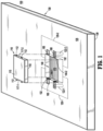
- FIG. 1 is a perspective exploded view of an example antenna apparatus, 100, according to an embodiment.
- Antenna apparatus 100 includes a substrate 130 and at least one antenna element 120 (e.g. two antenna elements 120-1, 120-2) electrically connected to RF circuitry within an IC chip 110.
- Each antenna element 120 is exemplified as a microstrip patch element printed on a lower surface 139 ("second outer surface") of substrate 130. While depicted with a rectangular shape, antenna element 120 may have any other suitable shape to form a desired radiation pattern. Further, other types of antenna elements such as dipoles or slot antenna elements may be substituted to realize target performance metrics.
- Substrate 130 has a cavity 140 formed within its top surface 135 ("first outer surface") and having a depth that extends to a bottom surface, which may coincide with a top surface of a ground plane 170.
- IC chip 110 is disposed within cavity 140 and a top surface 115 of IC chip 110 is substantially coplanar with a top surface 135 of substrate 130.
- a bottom surface 119 of IC chip 110 faces and may abut ground plane 170.
- At least one first edge contact 132 is disposed at a sidewall 144 of cavity 140.
- At least one second edge contact 112 is located on a side surface 117 of IC chip 110, and is electrically connected to an adjacent first edge contact 132.
- One antenna element 120 may be fed with RF signals (in transmit and/or receive directions) by a probe feed embodied as a through-substrate-via (TSV) (hereafter, “conductive via” or just “via”) 122.
- TSV through-substrate-via
- Via 122 may electrically connect to a short conductive trace 168 which in turn electrically connects to a first edge contact 132, thus completing an electrical connection between antenna element 120 and RF circuitry within IC chip 110 connected to a second edge contact 112.
- IC chip 110 refers to one or more electronic circuits embodied within a small flat piece of semiconductor material.
- IC chip 110 may be a monolithic microwave IC (MMIC) composed of gallium arsenide (GaAs), indium phosphide (InP), silicon germanium (SiGe) or gallium nitride (GaN).
- MMIC monolithic microwave IC
- IC chip 110 may include a power amplifier for amplifying a transmit path signal output to antenna element 120 and/or may include a low noise amplifier (LNA) for amplifying a receive path signal received by antenna element 120.
- LNA low noise amplifier
- two antenna elements 120-1, 120-2 are connected to a single IC chip 110 through a combination of vias 122-1, 122-2; first edge contacts 132 on opposite sidewalls 144-1, 144-2 of cavity 140; and second edge contacts 112 on opposite side surfaces 117-1, 117-2 of IC chip 110, respectively.
- IC chip 110 includes another pair of second edge contacts 112 each connected to one conductive trace 165 through an adjacent first edge contact 132.
- Each conductive trace 165 may electrically connect to a component (not shown) such as a terminal that receives a bias voltage or a control signal applied to an RF component within IC chip 110 such as an amplifier or a dynamically controlled phase shifter.
- IC chip 110 includes more or fewer edge contacts 112 to make more or fewer connections to components as desired for a particular application; and more or fewer antenna elements 120 are connected to IC chip 110.
- CPW coplanar waveguide
- conductive traces 165 and 168 in the drawings herein are shown as single lines; in the case of microstrip, conductive traces 165 may be microstrip lines over a ground plane (e.g., 170).
- conductive traces 165 may each be an inner conductive trace in between a pair of outer conductive ground traces (albeit not shown in the figures).
- Antenna apparatus 100 is comprised of at least one IC chip 110 and at least one antenna element 120 as shown in FIG. 1 .
- antenna apparatus 110 is comprised of several, tens or hundreds IC chips 110, each within a respective cavity 140 spatially arranged along substrate 130.
- at least some, or all, of the IC chips 110 are respectively connected to one or more antenna elements 120 spatially arranged along substrate 130's lower surface 139, thereby forming an antenna array.
- the antenna array may be an electronically steered antenna such as a phased array dynamically steered by phase shifters collectively located within the IC chips 110 or elsewhere within antenna apparatus 100.
- Substrate 130 may include beamforming circuitry electrically coupled to the IC chips 110 to divide an input RF signal during a transmit operation and/or combine a plurality of RF signals received from the antenna elements 120 and processed (e.g. amplified, filtered, phase shifted, down-converted, etc.) by IC chips 110 during a receive operation.
- beamforming circuitry electrically coupled to the IC chips 110 to divide an input RF signal during a transmit operation and/or combine a plurality of RF signals received from the antenna elements 120 and processed (e.g. amplified, filtered, phase shifted, down-converted, etc.) by IC chips 110 during a receive operation.
- FIG. 2 is a plan view of antenna apparatus 100 of FIG. 1 in an assembled state.
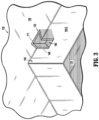
- FIG. 3 is a perspective view illustrating an example first edge contact 132 on a cavity sidewall.
- FIG. 4 is a perspective view illustrating an example second edge contact 112 formed on a side surface of IC chip 110.
- FIG. 5 is a cross-sectional view taken along the lines 5-5 of FIG. 2 .
- a first edge contact 132 and an adjacent second edge contact 112 may have complementary geometric shapes.
- Each first edge contact 132 may have metallic peripheral surfaces in a three dimensional (3D) structure, e.g., a 3D structure plated to form side, base and rear metallic peripheral surfaces.
- 3D three dimensional
- the dimensions of the complementary geometric structures may form a close fit to enable IC chip 110 to be placed within cavity 140 so that the second edge contacts 112 "snap in" to the first edge contacts 132. This may help secure IC chip 110 in place within cavity 140 prior to any electrical connection enhancement between the edge contacts 112, 132 through soldering, thermocompression, thermasonic bonding, or the like. Alternatively, a complete electrical connection can be made by just a press fit between the edge contact structures, without any soldering, etc. The close fit between adjacent first and second edge contacts 132, 112 may cause the respective edge contacts to be interlocked. For instance, as seen in FIG.
- a first edge contact 132 may have a slotted, flared opening 149, which is a recess within cavity sidewall 144-2.
- An adjacent second edge contact 112 as best seen in FIG. 4 may be in the form of a flared protrusion from side surface 117-2 that closely fits within slotted opening 149.
- solder or other conductive bonding material 190 With the outer surfaces of second edge contacts 112 in close contact with the inner surfaces of corresponding first edge contacts 132, solder or other conductive bonding material 190 (see FIG. 2 ) may be applied therebetween to complete or enhance an electrical connection.
- the conductive bonding material may also serve at least partially as a mechanical connection of IC chip 110 to substrate 130.
- IC chip 110 may also form a close fit or even a press fit with respect to the sidewalls 144 of cavity 140.
- a small gap “g” may exist between a side surface 117 of IC chip 110 and a sidewall 144 to allow for thermal expansion or manufacturing tolerances.
- a ground-signal-ground (GSG) snap connection may be made between corresponding edge contacts 112, 132.
- GSG ground-signal-ground
- a second edge contact 112 may be comprised of three contacts: one "signal" contact between and electrically isolated from two "ground” contacts.
- a corresponding first edge contact 132 also includes three connection points comprised of one signal contact between two ground contacts.
- first and second edge contacts 112, 132 are each embodied with a dielectric waveguide structure such as an optical conduit akin to optical fiber.
- conductive trace 165 is substituted with an optical conduit (hereafter, optical conduit 165 in this context) to permit an externally provided RF modulated laser to propagate to electronics within IC chip 110 through the optical conduit connection of first and second edge contacts 112, 132.
- An optical-RF converter within IC chip 110 converts the optical signal to an RF signal, which is output to antenna elements 120 through a different edge contact pair 112, 132.
- a signal is input to IC chip 110 as "RF over fiber" and is then converted to RF within IC chip 110 and radiated through antenna elements 120 in a transmit direction.
- an RF signal received by antenna elements 120 is routed to IC chip 110 through a pair of edge contacts 112, 132.
- IC chip 110 then converts the receive path RF signal to an optical signal that is routed through the same or different optical conduit 165 to an external system for processing.
- a high bandwidth system may be realizable with this approach.
- first edge contact 132 may have been constructed by first forming a notch within the top surface 135 of substrate 130 of the desired geometry for the edge contact by laser drilling, photo imaging and etching, or the like.
- the notch may have then been metalized through electroplating to form conductive sidewalls and a conductive base, and a front portion of the notch sliced away to form a front opening.
- first edge contact 132 having a front surface 146 approximately coplanar with side surface 144-2, a depth d1 (see FIG. 5 ), and a rear surface 171.
- the notches are completely filled with metal and later laser drilled to form a conductive structure with a desired geometry. Further discussion of forming first edge contacts 132 is provided later in connection with FIG. 6 .
- second edge contacts 112 these may be formed using various techniques.
- edge contacts 112 may be a quilt package nodule.
- first and second edge contacts 132, 112 are contemplated.
- the shapes for the recesses / protrusions may be rectangular, circular, oval, triangular and/or some other shape instead of the flare shape described above.
- an edge contact 132 may have an interdigitated structure with several metallic "fingers" or ridges and channels.
- an adjacent edge contact 112 may also have an interdigitated structure with complementary interlocking fingers or channels and ridges.
- interlocking structures on one or more sidewalls 144 of cavity 140 and one or more side surfaces 117 of chip 110 may be formed mostly or entirely of dielectric or semiconductor material.
- edge contacts 132 and 112 may be smaller than the interlocking structures and may be located either on surfaces of the interlocking structures themselves, on other portions of the sidewalls 144 / side surfaces 117, or they may form other complete interlocking structures.
- the smaller edge contacts if any, may have flat edges that abut one another, or they may have small complementary geometries.
- second contacts 132 instead of forming second contacts 132 as recesses, they may be formed as protrusions while the second edge contacts 112 are formed as recesses.
- each of the edge contacts 112, 132 are protrusions, e.g., flat or slanted, that abut an adjacent edge contact 132, 112, respectively.
- edge contacts 112, 132 may be used for conducting energy from DC to mm wave frequencies, and are particularly useful for forming low loss connections at mm wave frequencies. Since the electrical connection between adjacent edge contacts 112 and 132 is made without the use of bondwires or ribbon bonds, the inductance otherwise added by those techniques is eliminated. This results in an extremely low loss connection at frequencies up to at least 200GHz. Further, the overall configuration including cavity 140, first edge contacts 132 and IC chip 110 with second edge contacts 112, form a compact, thin structure in which the top surfaces 115 of chips 110 may be substantially coplanar with the top surface of substrate 130. Electrical and mechanical connection of IC chips 110 to substrate 130 are simplified, as IC chips 110 may be simply snapped into cavities 140 through the interlocking of edge contacts 112, 132, completing both mechanical and electrical connections.
- Substrate 130 may be a multi-layered substrate with circuitry disposed at different layers.
- Substrate 130 may be composed of any suitable dielectric material.
- substrate 130 is a hard substrate such as quartz, alumina, glass or fused silica, and amenable to thin film plating to form fine features.
- substrate 130 is composed of a lower layer (interchangeably, "lower substrate”) 130a and an upper layer (“upper substrate”) 130b, with a ground plane 170 sandwiched therebetween.
- Substrate 130 may have been formed by first providing lower layer 130a, metallizing a top surface of lower layer 130a to form ground plane 170, and thereafter forming or bonding upper layer 130b on ground plane 170 using a suitable method. Some exemplary methods for such bonding include dbi bonding, frit bonding, gold bump bonding, solder bump bonding, and copper pillar bonding. Alternatively, upper layer 130b may be separately provided and may have been adhered to ground plane 170 using a suitable adhesive. Ground plane 170 may have circular apertures 182 for accommodating vias 122-1 and 122-2.
- Apertures 182 have large enough diameters to allow vias 122-1, 122-2 to penetrate without contacting ground plane 170, thereby enabling vias 122-1, 122-2 to function as probe feeds for antenna elements 120-1, 120-2.
- Ground plane 170 may serve as a microstrip ground plane to reflect RF energy transmitted / received by antenna elements 120.
- the microstrip ground plane can also form the ground plane of a microstrip transmission line in which conductive trace 165 is the conductor.
- IC chip 110 may have a thickness approximately equal to a depth d2 from top surface 135 of substrate 130 to a top surface of ground plane 170 at the base of cavity 140. With such dimensions, the bottom surface 119 of IC chip 110 may rest on ground plane 170, and the top surface 115 of IC chip 110 may be approximately coplanar with top surface 135 of substrate 130. Alternatively, the thickness of IC chip 110 is less than depth d2 and a gap exists between ground plane 170 and bottom surface 119. Such a gap may be an air gap or a gap filled with a layer of insulating material. In some designs, it may be desirable for IC chip 110 to have one or more electrical contacts on the bottom surface 119 of IC chip 110 to make electrical connections to other components of antenna apparatus 100. In this case, corresponding apertures in ground plane 170 may be formed to facilitate the electrical connections.
- Conductive vias 122-1, 122-2 are examples of conductors, and form probe feeds for antenna elements 120-1, 120-2.
- a via 122 may be formed by first forming a pad on an outer surface of substrate 130, then drilling a hole through substrate 130 and filling the same with metal through electroplating or the like.
- a short conductive trace 168 on top surface 135 of substrate 130 may be an extension of such a via pad (or conductive trace 168 may itself be considered the via pad) and may interconnect a via 122 with a proximate first edge contact 132, e.g., by overlapping edge 171 of the first edge contact 132.
- conductive traces 165 connected to circuit components or terminals (not shown) other than an antenna element 120 may also be formed on surface 135 overlapping an edge 171 of a first edge contact 132 for electrical connection to the connected second edge contact 112. Any conductive trace 165 may make such electrical connection through another via (not shown) through substrate 130, or through a side port. Any conductive trace 165 may route an RF signal, a DC bias voltage, or a time varying control signal to / from IC chip 110 and the other circuit component.
- FIG. 6 is flow diagram of an example method, 600, of forming antenna apparatus 100.
- FIGS. 7A-7I are each cross-sectional views or plan views illustrating structures corresponding to respective steps in method 600. Note that the order of the various process steps described below for method 600 may be changed as desired in other example embodiments.
- FIG. 7A is a top plan view of a portion of a lower substrate 130a during a process stage after pattern metallization of top and bottom surfaces thereof has been performed.
- FIG. 7B is a cross-sectional view of the lower substrate 130a of FIG. 7A taken along the lines 7B-7B, and
- FIG. 7C is a bottom view of lower substrate 130a of FIG. 7A .
- lower substrate 130a is provided (S602), and the top and bottom surfaces of lower substrate 130a are masked in selective regions and metallized to form antenna elements 120 on the bottom surface and a ground plane 170 on the top surface.
- regions for forming apertures 182 in ground plane 170 may have been masked on the top surface and regions outside the boundaries of antenna elements 120 may have been masked on the bottom surface.
- Apertures 182 have a first diameter to accommodate later formed via holes with a second, smaller diameter. The larger diameter apertures 182 prevent subsequent vias 122 (shown in FIGS. 1-5 ) that will form probe feeds to antenna elements 120, from electrically shorting to ground plane 170.
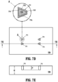
- FIG. 7D is a plan view of a portion of an upper substrate 130b, after notches 711 have been cut out to a depth d1 (less than the thickness d2 of upper substrate 130b) and metallized.
- FIG. 7E is a cross-sectional view of the upper substrate 130b of FIG. 7D taken along the lines 7E-7E.
- notches 711 are in the form of a flare, but other structures such as multi-fingers for forming interdigitated connections are also available.
- metallization of any notch 711 by means of electroplating or the like may produce sidewall metallization regions 717s, a front wall metallization region 717f, a rear wall metallization region 717r and a base metallization region 717b within the notch 711.
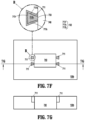
- FIG. 7F is a plan view of substrate 130b after a rectangular cutout 740 has been made between left and right notches 711.
- FIG. 7G is a cross-section of the upper substrate 130b in this stage taken along the lines 7G-7G. Cutout 740 later forms cavity 140 described earlier.
- a front portion of notch 711 may be sliced off so that the front metallization 717f of the notch 711 is removed. This opens up a slot within notch 711, thereby forming a first edge contact 132, within which a second edge contact 112 of IC chip 110 is later inserted.
- Areas adjacent to notches 711 may be metallized (S608) through pattern metallization to form either an adjacent upper via pad 168 or a conductive trace 165 electrically connected to the metallization in the notches.
- upper substrate 130b is attached / bonded to lower substrate 130a (S610) using a suitable bonding method or non-conductive adhesive to form a multi-layered substrate 130.
- a via hole may then be drilled (S612) between each via pad 168 and a corresponding antenna element 120, and the via holes metallized to complete probe feeds.
- FIG. 7H is a top plan view of a portion of the multi-layered substrate in an exemplary configuration after step S612.
- FIG. 7I is a cross-sectional view of FIG. 7H taken along the lines 7I-7I.
- a pair of conductive traces 165 and a pair of via pads 168 have each been formed on the top surface of upper substrate 130b.
- Via pads 168 / conductive traces 165 may thereby overlap and electrically connect to the rear wall metallization surface 717r of the adjacent first edge contact 132.
- adjacent shallower channels to form via pads 168 / conductive traces 165 may have been concurrently formed using the same laser drilling or etching process.
- via holes may be drilled in step S612 completely through the multi-layer structure. Each via hole may be drilled in a vertical path through a via pad 168, upper substrate 130b, an aperture 182, lower substrate 130a, and through an antenna element 120. The via holes may then be electroplated to complete probe feed vias to respective antenna elements 120.
- metallization may be built up in via regions 731 of antenna elements 120 and then a planarization process such as chemical mechanical polishing (CMP) may planarize the lower surfaces of antenna elements 120 and via regions 731, resulting in a flat, continuous lower metal surface for antenna elements 120.
- CMP chemical mechanical polishing
- an IC chip 110 may be provided (S614) with second edge contacts 112 each having a second geometrical shape complementary to the first geometrical shape of adjacent first edge contacts 132.
- the IC chip is snapped into cavity 140 as illustrated in FIG. 1 , resulting in a structure as shown in FIG. 7J , which illustrates second edge contacts 112 making electrical contact with metallized walls 717r, 717s and 717b of first edge contacts 132.
- second edge contacts 112 may snap into first edge contacts 132 thereby forming an interlocking relationship.
- a press fit between the contacts 112, 132 suffices in some cases to form an electrical connection therebetween and complete formation of antenna apparatus 100.
- the electrical connection between first and second edge contacts 112, 132 is enhanced using solder or other conductive bonding material 190 as depicted in FIG. 2 described earlier.
- Method 600 may be expanded to a method of fabricating an electronically steerable antenna array using the same operations described above but on an expanded scale by: (i) forming a plurality of cavities 140 each with at least one second edge contact 132 within substrate 130, where the plurality of cavities 140 are spatially arranged along the top surface of substrate 130; (ii) forming a plurality of antenna elements 120 or a plurality of sets of antenna elements 120 spatially arranged along the bottom surface of cavity 130 (i.e., along the bottom surface of lower substrate 130a); and (iii) snapping each of a plurality of IC chips 110 into a respective cavity 140, resulting in beamforming components within each IC chip 110 being electrically connected to at least one antenna element 120 through at least one respective conductive via 122.
- the expanded method includes, for each of the cavities 140: forming a second edge contact 132 at a sidewall of the cavity 140; placing a respective one of the IC chips 110 into the cavity 140; electrically connecting the respective first and second edge contacts 132, 112 (which may occur when the IC chip 110 is snapped into the cavity 140); and electrically connecting the beamforming components of the IC chip 110 placed therein to a respective at least one of the antenna elements 120 (which also may occur when the IC chip 110 is snapped into the cavity 140).
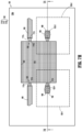
- FIG. 8A is a plan view of an electronic device, 800, in accordance with another embodiment.
- FIG. 8B is a cross-sectional view taken along the lines 8B-8B of FIG. 8A .
- electronic device 800 is an antenna apparatus having at least one antenna element, e.g., antenna elements 820-1, 820-2, 820-3, 820-4 electrically connected to an IC chip 110'. This example will be primarily described hereafter.
- electronic device 800 is a non-antenna implementation that omits antenna elements 820-1 to 820-4.
- antenna apparatus 800 when discussing an antenna implementation, electronic device 800 will be referred to as antenna apparatus 800.
- Antenna apparatus 800 differs from the above-described antenna apparatus 100 primarily by using a probe feed connection to at least one component, e.g., an antenna element, through a connection at a bottom surface of IC chip 110', rather than through edge contacts 112, 132.
- Substrate 130' is a multi-layered substrate comprised of lower substrate 130a' bonded to upper substrate 130b' and may be substantially the same as substrate 130 except for the locations of apertures 840-1, 840-2, 840-3, 840-4 within an embedded ground plane 870.
- first to fourth antenna elements 820-1 to 820-4 may be disposed on bottom surface 139 of substrate 130'.
- IC chip 110' may include at least one bottom contact, e.g., first to fourth bottom contacts 830-1, 830-2, 830-3, 830-4 centrally located within respective apertures 840-1 to 840-4 within ground plane 870.
- Bottom contacts 830-1 to 830-4 may each include a connection element such as a solder bump or copper pillar on an outer surface thereof for electrical connection to vias 822-1, 822-2, 822-3 and 822-4, respectively.
- the connection element e.g., solder bump / copper pillar
- each illustrated contact 830 is understood to include a bottom contact of IC chip 110' and the connection element).
- Vias 822-1 to 822-4 are probe feeds each electrically connected between a respective feed point of antenna element 820-1 to 820-4 and an electrical contact 830-1 to 830-4.
- Electrical contacts 830 may each connect to RF transmitter and/or receiver circuitry disposed within IC chip 110' for handling signal transmission / reception with respect to an antenna element 820.
- Antenna apparatus 800 includes at least one first edge contact 132 formed at a sidewall 144 of cavity 140 for connection to a corresponding at least one second edge contact 112 of IC chip 110'.
- Each conductive trace 165 connects to an adjacent first edge contact 132 in the same manner described above, for completing an electrical connection between another component / terminal of antenna apparatus 800 and RF circuitry within IC chip 110'.
- four conductive traces 165 are provided for connection to respective second edge contacts 112. Any conductive trace 165 may connect to the component / terminal through a side contact on substrate 130' or through a via (neither shown).
- At most three bottom contacts 830 are connected to at most three antenna elements 820 through vias 822, but at least one other antenna element 820 is electrically connected to IC chip 110' through one set of edge contacts 132, 112 and a via extending from the top surface of substrate 130'.
- at least one other bottom contact 830 may connect to a conductive trace 165 (not shown) embedded within lower substrate 130a' for connection to another component to exchange RF signals, control signals or DC bias, or to ground plane 870 to make a ground connection.
- At least one bottom contact 830 is connected to an inter-layer via (e.g., a shortened version of via 822-1) that connects to a conductive trace 165 (both not shown) extending within lower substrate layer 130a'.
- ground plane 870 or portion thereof is replaced by a metal layer configured as a thermal heat sink to cool IC chip 110', while at least one bottom contact 830 is connected to an inter-layer via similarly connected to a conductive trace 165.
- FIG. 9 is a flow diagram illustrating an example method 900 of fabricating electronic device 800.
- lower substrate 130a' and upper substrate 130b' may be separately processed and then bonded together.
- IC chip 110' is then snapped into the central cavity 140 and electrical connections between respective contacts of IC chip 110' to those formed within substrate 130' are made.
- lower substrate 130a' having top and bottom surfaces is provided (S902). Regions of the top and bottom surfaces are masked for pattern metallization to form antenna elements 120 on the bottom surface and ground plane 870 on the top surface with apertures 840 and via pads (upper part of vias 830) within the apertures. Via holes are then drilled (S903) through the via pads to the bottom surface at feed points to the antenna elements. The via holes are metalized to complete probe feeds.
- Upper substrate 130b' may then be processed in steps S904, S906, S908 and S908 in the same manner as steps S604, S606, S608 and S608, respectively, except that each edge contact 132 may connect to a conductive trace 165 instead of a via 168.
- process steps S904-S908 may be the same as S604-S608.
- Upper substrate 130b' is then attached / bonded to lower substrate 130a' (S910) using a bonding method or a non-conductive adhesive 789.
- suitable bonding methods for this purpose include dbi bonding, frit bonding, gold bump bonding, solder bump bonding, and copper pillar bonding.
- IC chip 110' may be provided (S912) with complementary (second) edge contacts 112, and with bottom contacts 830-1 to 830-4 having attached solder bumps or copper pillars. IC chip 110' is snapped into cavity 140 and electrical connection is made between corresponding first and second edge contacts 132, 112 in the manner described earlier. Electrical connection between bottom electrical contacts 830 and respective vias 822 may be made by heating and cooling the solder bumps / copper pillars attached to electrical contacts 830. Note that the solder bumps / copper pillars may be alternatively attached to the ends of vias 822 after their formation, instead of to electrical contacts 830, and thereafter the electrical connection of vias 822 to electrical contacts 830 may be made using the same heating and cooling technique.
- FIG. 10A is an exploded cross-sectional view of an electronic device, 10, with embedded IC chips according to another embodiment.
- FIG. 10B is a cross-sectional view of electronic device 10 in an assembled state.
- electronic device 10 includes a multi-layer substrate 30 with a dual cavity structure formed within a top surface 35; a first IC chip 60; and a second IC chip 50.
- First and second IC chips 60, 50 are disposed within respective first and second cavity portions 80, 70 of the dual cavity structure.
- First cavity portion 80 is directly below second cavity portion 70 and has a perimeter smaller than that of second cavity portion 70.
- First cavity portion 80 has at least one sidewall 81 at which one or more first edge contacts 132 is disposed, where each first edge contact 132 may be electrically connected to an adjacent second edge contact 112 disposed at a side surface 62 of IC chip 60.
- second cavity portion 60 has at least one first edge contact 132' electrically connected to at least one second edge contact 112' on a side surface 52 of IC chip 50.
- cavity portion 80 includes at least one first edge contact 132 at each of opposite sidewalls 81-1, 81-2; and second cavity portion 70 includes at least one first edge contact 132' at each of opposite sidewalls 71-1, 71-2 for connection to corresponding second edge contacts.
- Edge contacts 132, 132', 112, 112' may have the same or similar structures to those described earlier, and may be fabricated and electrically connected to one another in the same or similar manner to that already described.
- Any edge contact 132 or 132' may electrically connect to another component of electronic device 10 through a via and /or a conductive trace within substrate 30.
- IC chips 50 and 60 may be electrically connected to one another through one or more sets of edge contacts 112, 132, 132' and 112'.
- substrate 30 may be composed of a lower layer 30a, a central layer 30b and an upper layer 30c.
- Conductive traces 165 may be disposed between layers 30a and 30b and between layers 30b and 30c.
- circuitry within first IC chip 60 may electrically connect to circuitry within second IC chip 50 through a path comprising a second edge contact 112, a first edge contact 132, a first conductive trace 165, a blind via 22 extending through substrate layer 30c, a via pad / second conductive trace 168, a first edge contact 132' and a second edge contact 112'.
- first IC chip 60 includes an amplifier electrically coupled to one or more antenna elements (not shown) disposed at a lower surface of substrate layer 30a.
- the amplifier of first IC chip 60 may be electrically connected to beamforming network circuitry included within second IC chip 50 through the above-noted connection path.
- several, tens or a multiplicity of IC chips 50 and 60 may be spatially arranged in cavities across substrate 30 to drive an antenna array such as a phased array.
- First IC chip 60 may be composed of a different semiconductor material than that of second IC chip 50.
- first IC chip 60 is composed of InP and second IC chip 50 is composed of SiGe.
- First IC chip 60 when assembled within first cavity portion 80, may have a top surface that is approximately coplanar with a top surface of first cavity portion 80.
- Second IC chip 50 may have a thickness dimension that is less than the depth of second cavity portion 70, such that when second IC chip 50 is assembled within second cavity portion 70, its top surface may be approximately coplanar with top surface 35 of substrate 30, but its bottom surface may be spaced from a top surface of second cavity portion 70 by a gap 97.
- gap 97 is an air gap.
- gap 97 is an insulating underfill material formed over first IC chip 60 after first IC chip 60 is assembled within first cavity portion 80. in the latter case, second IC chip 50 may be placed over the underfill material for assembly within second cavity portion 50.
- the underfill material may have apertures allowing for electrical connection between upper contacts formed on first IC chip 60 and lower contacts formed on second IC chip 50.
- a layer 87 of material may be disposed at a bottom surface of first cavity portion 80.
- layer 87 is a portion of a ground plane akin to ground planes 170 or 870 in the above-discussed embodiments.
- other ground plane portions (not shown) are disposed surrounding layer 87 between layers 30a and 30b, and all the ground plane portions together act as a ground plane for antenna elements disposed on the lower surface of substrate layer 30a.
- the collective ground plane may just form a ground surface for circuit paths between circuit components.
- Layer 87 may alternatively be configured to serve as a thermal heat sink.
- layer 87 is not a ground plane but is patterned to form one or more conductive traces for RF, DC or control signal connections between circuitry within first IC 60 and other circuit elements within electronic device 10.
- Electronic devices and antenna apparatus in accordance with the presently disclosed technology may exhibit certain advantages over conventional devices. For instance, due to the compact configurations as described, embodiments may allow for high performance signal routing at extremely high frequencies, e.g., on the order of 200GHz. Such high performance at least partially stems from the elimination or minimization of inductance from bondwires between the chip and conductive traces / vias on the substrate that would otherwise be employed. Embodiments may empower a next generation of such extremely high frequency phased arrays and other components. Compact, thin configurations are realizable with outer surfaces of the IC chips substantially coplanar with the outer substrate surface. Fabrication is simplified by means of the IC chips being simply snapped into the cavities of the multi-layer substrate and concurrently completing both mechanical and electrical connections through the interlocking of the first and second edge contacts.
Landscapes
- Engineering & Computer Science (AREA)
- Microelectronics & Electronic Packaging (AREA)
- Manufacturing & Machinery (AREA)
- Variable-Direction Aerials And Aerial Arrays (AREA)
- Details Of Aerials (AREA)
- Waveguide Aerials (AREA)
- Semiconductor Integrated Circuits (AREA)
Abstract
Description
- This disclosure relates generally to connection techniques and arrangements between IC chips and other circuit components supported by a substrate, such as printed antenna elements.
- In wireless communications it is typically desired to provide small sized antenna equipment in which antenna elements are integrated with IC chips containing beamforming components. Satellite applications, for example, typically employ phased arrays with many microstrip patch antenna elements disposed on a substrate. The antenna elements may be electrically coupled to distributed power amplifiers supplying RF power and to phase shifters controlled by a processor to dynamically steer the resulting antenna beam. The power amplifiers, phase shifters, and other front end equipment such as receiving circuitry, may be provided within IC chips integrated with the antenna elements in a unitary structure.
- In an aspect of the presently disclosed technology, an antenna apparatus includes a substrate having a cavity in a first outer surface thereof. The substrate has a sidewall defining a portion of the cavity, and a first edge contact is formed at the sidewall. An IC chip is disposed within the cavity and has a side surface facing the sidewall and a second edge contact formed on the side surface electrically connected to the first edge contact. An antenna element, disposed at a second outer surface of the substrate opposite the first outer surface, is electrically connected to RF circuitry within the IC chip through a conductive via extending within the substrate.
- The electrical connection of the antenna element to the RF circuitry within the IC chip may be made through the first and second edge contacts. Alternatively, the connection of the antenna element may be made from an electrical contact at a bottom surface of the IC chip.
- In another aspect, a method of fabricating an antenna apparatus involves forming a cavity in a first outer surface of a substrate, and forming an antenna element on a second outer surface of the substrate opposite the first outer surface. A first edge contact is formed at a sidewall of the cavity. An IC chip is placed into the cavity, where the IC chip has a second edge contact formed on a side surface thereof, and includes RF circuitry. The first and second edge contacts are electrically connected. A conductive via is formed extending from the second outer surface within the substrate, and the antenna element is electrically connected to the RF circuitry through the conductive via.
- In another aspect, a method of fabricating an electronically steerable antenna array, includes: forming within a substrate a plurality of cavities spatially arranged along a first outer surface of the substrate; forming a plurality of antenna elements spatially arranged on a second outer surface of the substrate opposite the first outer surface; providing a plurality of IC chips, each having a side surface with a respective first edge contact, each IC chip including beamforming components; for each of the cavities: forming a second edge contact on a sidewall of the cavity; placing a respective one of the plurality of IC chips into the cavity; electrically connecting the respective first and second edge contacts; and electrically connecting the beamforming components of the IC chip placed therein to a respective at least one of the antenna elements.
- The above and other aspects and features of the disclosed technology will become more apparent from the following detailed description, taken in conjunction with the accompanying drawings in which like reference characters indicate like elements or features. Various elements of the same or similar type may be distinguished by annexing the reference label with a dash and second label that distinguishes among the same / similar elements (e.g., -1, -2). However, if a given description uses only the first reference label, it is applicable to any one of the same / similar elements having the same first reference label irrespective of the second reference label. Elements and features may not be drawn to scale in the drawings.
-
FIG. 1 is a perspective exploded view of an example antenna apparatus according to an embodiment. -
FIG. 2 is a plan view of the antenna apparatus ofFIG. 1 in an assembled state. -
FIG. 3 is a perspective view illustrating an example first edge contact on a cavity sidewall. -
FIG. 4 is a perspective view illustrating an example second edge contact formed on a side surface of an IC chip. -
FIG. 5 is a cross-sectional view taken along the lines 5-5 of the antenna apparatus ofFIG. 2 . -
FIG. 6 is a flow diagram of an example method of forming the antenna apparatus ofFIGS. 1-5 . -
FIG. 7A is a top plan view of portion of a lower substrate, which forms part of a multi-layer substrate of an exemplary antenna apparatus, where the view illustrates an interim configuration after step S602 of the method ofFIG. 6 . -
FIG. 7B is a cross-sectional view of the lower substrate ofFIG. 7A taken along thelines 7B-7B. -
FIG. 7C is a bottom plan view of the lower substrate ofFIG. 7A . -
FIG. 7D is a plan view of a portion of an upper substrate of the multi-layer substrate in an interim process after step S604 ofFIG. 6 , and illustrates a configuration after notches for forming edge contacts have been cut out and metallized. -
FIG. 7E is a cross-sectional view of the upper substrate ofFIG. 7D taken along thelines 7E-7E. -
FIG. 7F is a plan view of the upper substrate ofFIG. 7D after step S606 ofFIG. 6 . -
FIG. 7G is a cross-sectional view of the upper substrate ofFIG. 7F taken along thelines 7G-7G. -
FIG. 7H is a top plan view of a portion of an exemplary multi-layered substrate which is formed after step S612 of the method ofFIG. 6 . -
FIG. 7I is a cross-sectional view ofFIG. 7H taken along the lines 7I-7I. -
FIG. 7J is a cross-sectional view corresponding to the cross sectional view ofFIG. 7I after step S614 ofFIG. 6 . -
FIG. 8A is a plan view of an electronic device in accordance with another embodiment. -
FIG. 8B is a cross-sectional view taken along thelines 8B-8B' ofFIG. 8A . -
FIG. 9 is a flow diagram illustrating an example method of fabricating the electronic device ofFIGS. 8A-8B . -
FIG. 10A is an exploded cross-sectional view of an electronic device with embedded chips according to an embodiment. -
FIG. 10B is a cross-sectional view of the electronic device ofFIG. 10A in an assembled state. - The following description, with reference to the accompanying drawings, is provided to assist in a comprehensive understanding of certain exemplary embodiments of the technology disclosed herein for illustrative purposes. The description includes various specific details to assist a person of ordinary skill the art with understanding the technology, but these details are to be regarded as merely illustrative. For the purposes of simplicity and clarity, descriptions of well-known functions and constructions may be omitted when their inclusion may obscure appreciation of the technology by a person of ordinary skill in the art.
-
FIG. 1 is a perspective exploded view of an example antenna apparatus, 100, according to an embodiment.Antenna apparatus 100 includes asubstrate 130 and at least one antenna element 120 (e.g. two antenna elements 120-1, 120-2) electrically connected to RF circuitry within anIC chip 110. Each antenna element 120 is exemplified as a microstrip patch element printed on a lower surface 139 ("second outer surface") ofsubstrate 130. While depicted with a rectangular shape, antenna element 120 may have any other suitable shape to form a desired radiation pattern. Further, other types of antenna elements such as dipoles or slot antenna elements may be substituted to realize target performance metrics. -
Substrate 130 has acavity 140 formed within its top surface 135 ("first outer surface") and having a depth that extends to a bottom surface, which may coincide with a top surface of aground plane 170. In an assembled state ofantenna apparatus 100,IC chip 110 is disposed withincavity 140 and atop surface 115 ofIC chip 110 is substantially coplanar with atop surface 135 ofsubstrate 130. In the assembled state, abottom surface 119 ofIC chip 110 faces and may abutground plane 170. At least onefirst edge contact 132 is disposed at a sidewall 144 ofcavity 140. At least onesecond edge contact 112 is located on a side surface 117 ofIC chip 110, and is electrically connected to an adjacentfirst edge contact 132. One antenna element 120 may be fed with RF signals (in transmit and/or receive directions) by a probe feed embodied as a through-substrate-via (TSV) (hereafter, "conductive via" or just "via") 122. Via 122 may electrically connect to a shortconductive trace 168 which in turn electrically connects to afirst edge contact 132, thus completing an electrical connection between antenna element 120 and RF circuitry withinIC chip 110 connected to asecond edge contact 112. - Herein, the term IC chip refers to one or more electronic circuits embodied within a small flat piece of semiconductor material. For example,
IC chip 110 may be a monolithic microwave IC (MMIC) composed of gallium arsenide (GaAs), indium phosphide (InP), silicon germanium (SiGe) or gallium nitride (GaN).IC chip 110 may include a power amplifier for amplifying a transmit path signal output to antenna element 120 and/or may include a low noise amplifier (LNA) for amplifying a receive path signal received by antenna element 120. - In the illustrated example, two antenna elements 120-1, 120-2 are connected to a
single IC chip 110 through a combination of vias 122-1, 122-2;first edge contacts 132 on opposite sidewalls 144-1, 144-2 ofcavity 140; andsecond edge contacts 112 on opposite side surfaces 117-1, 117-2 ofIC chip 110, respectively. Also,IC chip 110 includes another pair ofsecond edge contacts 112 each connected to oneconductive trace 165 through an adjacentfirst edge contact 132. Eachconductive trace 165 may electrically connect to a component (not shown) such as a terminal that receives a bias voltage or a control signal applied to an RF component withinIC chip 110 such as an amplifier or a dynamically controlled phase shifter. In other examples,IC chip 110 includes more orfewer edge contacts 112 to make more or fewer connections to components as desired for a particular application; and more or fewer antenna elements 120 are connected toIC chip 110. For RF connections, microstrip or coplanar waveguide (CPW) transitions may be made. For instance,conductive traces conductive traces 165 may be microstrip lines over a ground plane (e.g., 170). In the case of CPW,conductive traces 165 may each be an inner conductive trace in between a pair of outer conductive ground traces (albeit not shown in the figures). -
Antenna apparatus 100 is comprised of at least oneIC chip 110 and at least one antenna element 120 as shown inFIG. 1 . In a typical application,antenna apparatus 110 is comprised of several, tens orhundreds IC chips 110, each within arespective cavity 140 spatially arranged alongsubstrate 130. In this typical application, at least some, or all, of the IC chips 110 are respectively connected to one or more antenna elements 120 spatially arranged alongsubstrate 130'slower surface 139, thereby forming an antenna array. The antenna array may be an electronically steered antenna such as a phased array dynamically steered by phase shifters collectively located within the IC chips 110 or elsewhere withinantenna apparatus 100.Substrate 130 may include beamforming circuitry electrically coupled to the IC chips 110 to divide an input RF signal during a transmit operation and/or combine a plurality of RF signals received from the antenna elements 120 and processed (e.g. amplified, filtered, phase shifted, down-converted, etc.) byIC chips 110 during a receive operation. -
FIG. 2 is a plan view ofantenna apparatus 100 ofFIG. 1 in an assembled state.FIG. 3 is a perspective view illustrating an examplefirst edge contact 132 on a cavity sidewall.FIG. 4 is a perspective view illustrating an examplesecond edge contact 112 formed on a side surface ofIC chip 110.FIG. 5 is a cross-sectional view taken along the lines 5-5 ofFIG. 2 . Referring collectively toFIGS. 1-5 , afirst edge contact 132 and an adjacentsecond edge contact 112 may have complementary geometric shapes. Eachfirst edge contact 132 may have metallic peripheral surfaces in a three dimensional (3D) structure, e.g., a 3D structure plated to form side, base and rear metallic peripheral surfaces. The dimensions of the complementary geometric structures may form a close fit to enableIC chip 110 to be placed withincavity 140 so that thesecond edge contacts 112 "snap in" to thefirst edge contacts 132. This may help secureIC chip 110 in place withincavity 140 prior to any electrical connection enhancement between theedge contacts second edge contacts FIG. 3 , afirst edge contact 132 may have a slotted, flaredopening 149, which is a recess within cavity sidewall 144-2. An adjacentsecond edge contact 112 as best seen inFIG. 4 may be in the form of a flared protrusion from side surface 117-2 that closely fits within slottedopening 149. With the outer surfaces ofsecond edge contacts 112 in close contact with the inner surfaces of correspondingfirst edge contacts 132, solder or other conductive bonding material 190 (seeFIG. 2 ) may be applied therebetween to complete or enhance an electrical connection. The conductive bonding material may also serve at least partially as a mechanical connection ofIC chip 110 tosubstrate 130. The outer dimensions ofIC chip 110 may also form a close fit or even a press fit with respect to the sidewalls 144 ofcavity 140. A small gap "g" may exist between a side surface 117 ofIC chip 110 and a sidewall 144 to allow for thermal expansion or manufacturing tolerances. - If a coplanar waveguide (CPW) transition is used for the
edge contacts corresponding edge contacts second edge contact 112 may be comprised of three contacts: one "signal" contact between and electrically isolated from two "ground" contacts. A correspondingfirst edge contact 132 also includes three connection points comprised of one signal contact between two ground contacts. - In an alternative embodiment, corresponding first and
second edge contacts conductive trace 165 is substituted with an optical conduit (hereafter,optical conduit 165 in this context) to permit an externally provided RF modulated laser to propagate to electronics withinIC chip 110 through the optical conduit connection of first andsecond edge contacts IC chip 110 converts the optical signal to an RF signal, which is output to antenna elements 120 through a differentedge contact pair IC chip 110 as "RF over fiber" and is then converted to RF withinIC chip 110 and radiated through antenna elements 120 in a transmit direction. In a receive direction, an RF signal received by antenna elements 120 is routed toIC chip 110 through a pair ofedge contacts IC chip 110 then converts the receive path RF signal to an optical signal that is routed through the same or differentoptical conduit 165 to an external system for processing. A high bandwidth system may be realizable with this approach. - In the tapered slot design of
first edge contact 132 as shown inFIG. 3 ,first edge contact 132 may have been constructed by first forming a notch within thetop surface 135 ofsubstrate 130 of the desired geometry for the edge contact by laser drilling, photo imaging and etching, or the like. The notch may have then been metalized through electroplating to form conductive sidewalls and a conductive base, and a front portion of the notch sliced away to form a front opening. This results infirst edge contact 132 having afront surface 146 approximately coplanar with side surface 144-2, a depth d1 (seeFIG. 5 ), and arear surface 171. Alternatively, the notches are completely filled with metal and later laser drilled to form a conductive structure with a desired geometry. Further discussion of formingfirst edge contacts 132 is provided later in connection withFIG. 6 . With regard tosecond edge contacts 112, these may be formed using various techniques. For example,edge contacts 112 may be a quilt package nodule. - Other geometries and other types of structures for first and
second edge contacts centralized slot 149, anedge contact 132 may have an interdigitated structure with several metallic "fingers" or ridges and channels. In this case, anadjacent edge contact 112 may also have an interdigitated structure with complementary interlocking fingers or channels and ridges. In other examples, interlocking structures on one or more sidewalls 144 ofcavity 140 and one or more side surfaces 117 ofchip 110 may be formed mostly or entirely of dielectric or semiconductor material. In this case,edge contacts second contacts 132 as recesses, they may be formed as protrusions while thesecond edge contacts 112 are formed as recesses. Alternatively, each of theedge contacts adjacent edge contact edge contacts adjacent edge contacts configuration including cavity 140,first edge contacts 132 andIC chip 110 withsecond edge contacts 112, form a compact, thin structure in which thetop surfaces 115 ofchips 110 may be substantially coplanar with the top surface ofsubstrate 130. Electrical and mechanical connection ofIC chips 110 tosubstrate 130 are simplified, asIC chips 110 may be simply snapped intocavities 140 through the interlocking ofedge contacts -
Substrate 130 may be a multi-layered substrate with circuitry disposed at different layers.Substrate 130 may be composed of any suitable dielectric material. In some embodiments,substrate 130 is a hard substrate such as quartz, alumina, glass or fused silica, and amenable to thin film plating to form fine features. As seen inFIG. 5 , for example,substrate 130 is composed of a lower layer (interchangeably, "lower substrate") 130a and an upper layer ("upper substrate") 130b, with aground plane 170 sandwiched therebetween.Substrate 130 may have been formed by first providinglower layer 130a, metallizing a top surface oflower layer 130a to formground plane 170, and thereafter forming or bondingupper layer 130b onground plane 170 using a suitable method. Some exemplary methods for such bonding include dbi bonding, frit bonding, gold bump bonding, solder bump bonding, and copper pillar bonding. Alternatively,upper layer 130b may be separately provided and may have been adhered toground plane 170 using a suitable adhesive.Ground plane 170 may havecircular apertures 182 for accommodating vias 122-1 and 122-2.Apertures 182 have large enough diameters to allow vias 122-1, 122-2 to penetrate without contactingground plane 170, thereby enabling vias 122-1, 122-2 to function as probe feeds for antenna elements 120-1, 120-2.Ground plane 170 may serve as a microstrip ground plane to reflect RF energy transmitted / received by antenna elements 120. The microstrip ground plane can also form the ground plane of a microstrip transmission line in whichconductive trace 165 is the conductor. -
IC chip 110 may have a thickness approximately equal to a depth d2 fromtop surface 135 ofsubstrate 130 to a top surface ofground plane 170 at the base ofcavity 140. With such dimensions, thebottom surface 119 ofIC chip 110 may rest onground plane 170, and thetop surface 115 ofIC chip 110 may be approximately coplanar withtop surface 135 ofsubstrate 130. Alternatively, the thickness ofIC chip 110 is less than depth d2 and a gap exists betweenground plane 170 andbottom surface 119. Such a gap may be an air gap or a gap filled with a layer of insulating material. In some designs, it may be desirable forIC chip 110 to have one or more electrical contacts on thebottom surface 119 ofIC chip 110 to make electrical connections to other components ofantenna apparatus 100. In this case, corresponding apertures inground plane 170 may be formed to facilitate the electrical connections. - Conductive vias 122-1, 122-2 are examples of conductors, and form probe feeds for antenna elements 120-1, 120-2. As described further below, a via 122 may be formed by first forming a pad on an outer surface of
substrate 130, then drilling a hole throughsubstrate 130 and filling the same with metal through electroplating or the like. A shortconductive trace 168 ontop surface 135 ofsubstrate 130 may be an extension of such a via pad (orconductive trace 168 may itself be considered the via pad) and may interconnect a via 122 with a proximatefirst edge contact 132, e.g., by overlappingedge 171 of thefirst edge contact 132. Otherconductive traces 165 connected to circuit components or terminals (not shown) other than an antenna element 120 may also be formed onsurface 135 overlapping anedge 171 of afirst edge contact 132 for electrical connection to the connectedsecond edge contact 112. Anyconductive trace 165 may make such electrical connection through another via (not shown) throughsubstrate 130, or through a side port. Anyconductive trace 165 may route an RF signal, a DC bias voltage, or a time varying control signal to / fromIC chip 110 and the other circuit component. -
FIG. 6 is flow diagram of an example method, 600, of formingantenna apparatus 100.FIGS. 7A-7I are each cross-sectional views or plan views illustrating structures corresponding to respective steps inmethod 600. Note that the order of the various process steps described below formethod 600 may be changed as desired in other example embodiments. - To form
multi-layer substrate 130 ofantenna apparatus 100,lower substrate 130a andupper substrate 130b may be separately processed and then bonded together.FIG. 7A is a top plan view of a portion of alower substrate 130a during a process stage after pattern metallization of top and bottom surfaces thereof has been performed.FIG. 7B is a cross-sectional view of thelower substrate 130a ofFIG. 7A taken along thelines 7B-7B, andFIG. 7C is a bottom view oflower substrate 130a ofFIG. 7A . Referring toFIGS. 6 and7A-7C ,lower substrate 130a is provided (S602), and the top and bottom surfaces oflower substrate 130a are masked in selective regions and metallized to form antenna elements 120 on the bottom surface and aground plane 170 on the top surface. Prior to this metallization, regions for formingapertures 182 inground plane 170 may have been masked on the top surface and regions outside the boundaries of antenna elements 120 may have been masked on the bottom surface.Apertures 182 have a first diameter to accommodate later formed via holes with a second, smaller diameter. Thelarger diameter apertures 182 prevent subsequent vias 122 (shown inFIGS. 1-5 ) that will form probe feeds to antenna elements 120, from electrically shorting toground plane 170. - An upper substrate with top and bottom surfaces is separately provided and processed (S604). This process may involve cutting left and right notches in the top surface, each having a first geometrical shape(s), using laser drilling, mechanical drilling, photo imaging or etching, or other suitable technique. The notches are then metallized to form the first edge contacts 132 (with some metallization sliced away afterwards during another cut-out process). For instance,
FIG. 7D is a plan view of a portion of anupper substrate 130b, afternotches 711 have been cut out to a depth d1 (less than the thickness d2 ofupper substrate 130b) and metallized.FIG. 7E is a cross-sectional view of theupper substrate 130b ofFIG. 7D taken along thelines 7E-7E. In thisexample notches 711 are in the form of a flare, but other structures such as multi-fingers for forming interdigitated connections are also available. As seen in the enlargement A, metallization of anynotch 711 by means of electroplating or the like may producesidewall metallization regions 717s, a frontwall metallization region 717f, a rearwall metallization region 717r and abase metallization region 717b within thenotch 711. - A central cutout for the IC chip may then be made (S604) through the top substrate. For example,
FIG. 7F is a plan view ofsubstrate 130b after arectangular cutout 740 has been made between left andright notches 711.FIG. 7G is a cross-section of theupper substrate 130b in this stage taken along thelines 7G-7G.Cutout 740later forms cavity 140 described earlier. As depicted in the enlargement B, whencutout 740 is made, a front portion ofnotch 711 may be sliced off so that thefront metallization 717f of thenotch 711 is removed. This opens up a slot withinnotch 711, thereby forming afirst edge contact 132, within which asecond edge contact 112 ofIC chip 110 is later inserted. - Areas adjacent to
notches 711 may be metallized (S608) through pattern metallization to form either an adjacent upper viapad 168 or aconductive trace 165 electrically connected to the metallization in the notches. Before or after such metallization,upper substrate 130b is attached / bonded tolower substrate 130a (S610) using a suitable bonding method or non-conductive adhesive to form amulti-layered substrate 130. A via hole may then be drilled (S612) between each viapad 168 and a corresponding antenna element 120, and the via holes metallized to complete probe feeds. - For example,
FIG. 7H is a top plan view of a portion of the multi-layered substrate in an exemplary configuration after step S612.FIG. 7I is a cross-sectional view ofFIG. 7H taken along the lines 7I-7I. In the example, a pair ofconductive traces 165 and a pair of viapads 168 have each been formed on the top surface ofupper substrate 130b. Viapads 168 /conductive traces 165 may thereby overlap and electrically connect to the rearwall metallization surface 717r of the adjacentfirst edge contact 132. Alternatively, whennotches 711 are initially formed, adjacent shallower channels to form viapads 168 /conductive traces 165 may have been concurrently formed using the same laser drilling or etching process. Then, whennotches 711 are metallized, the shallower channels are metallized during the same metallization process, thereby forming viapads 168 /conductive traces 165 with a top surface coplanar with the top surface ofrear metallization 717r. In still another alternative, viapads 168 andconductive traces 165 are completed prior to formingnotches 711 andfirst edge contacts 132. - Once via
pads 168 are formed, via holes may be drilled in step S612 completely through the multi-layer structure. Each via hole may be drilled in a vertical path through a viapad 168,upper substrate 130b, anaperture 182,lower substrate 130a, and through an antenna element 120. The via holes may then be electroplated to complete probe feed vias to respective antenna elements 120. In this process, metallization may be built up in viaregions 731 of antenna elements 120 and then a planarization process such as chemical mechanical polishing (CMP) may planarize the lower surfaces of antenna elements 120 and viaregions 731, resulting in a flat, continuous lower metal surface for antenna elements 120. - With the
multi-layer substrate 130 thus formed, anIC chip 110 may be provided (S614) withsecond edge contacts 112 each having a second geometrical shape complementary to the first geometrical shape of adjacentfirst edge contacts 132. The IC chip is snapped intocavity 140 as illustrated inFIG. 1 , resulting in a structure as shown inFIG. 7J , which illustratessecond edge contacts 112 making electrical contact with metallizedwalls first edge contacts 132. - As discussed earlier,
second edge contacts 112 may snap intofirst edge contacts 132 thereby forming an interlocking relationship. A press fit between thecontacts antenna apparatus 100. In other cases, the electrical connection between first andsecond edge contacts conductive bonding material 190 as depicted inFIG. 2 described earlier. -
Method 600 may be expanded to a method of fabricating an electronically steerable antenna array using the same operations described above but on an expanded scale by: (i) forming a plurality ofcavities 140 each with at least onesecond edge contact 132 withinsubstrate 130, where the plurality ofcavities 140 are spatially arranged along the top surface ofsubstrate 130; (ii) forming a plurality of antenna elements 120 or a plurality of sets of antenna elements 120 spatially arranged along the bottom surface of cavity 130 (i.e., along the bottom surface oflower substrate 130a); and (iii) snapping each of a plurality ofIC chips 110 into arespective cavity 140, resulting in beamforming components within eachIC chip 110 being electrically connected to at least one antenna element 120 through at least one respective conductive via 122. In other words, the expanded method includes, for each of the cavities 140: forming asecond edge contact 132 at a sidewall of thecavity 140; placing a respective one of the IC chips 110 into thecavity 140; electrically connecting the respective first andsecond edge contacts 132, 112 (which may occur when theIC chip 110 is snapped into the cavity 140); and electrically connecting the beamforming components of theIC chip 110 placed therein to a respective at least one of the antenna elements 120 (which also may occur when theIC chip 110 is snapped into the cavity 140). -
FIG. 8A is a plan view of an electronic device, 800, in accordance with another embodiment.FIG. 8B is a cross-sectional view taken along thelines 8B-8B ofFIG. 8A . In one implementation,electronic device 800 is an antenna apparatus having at least one antenna element, e.g., antenna elements 820-1, 820-2, 820-3, 820-4 electrically connected to an IC chip 110'. This example will be primarily described hereafter. In other embodiments, discussed below,electronic device 800 is a non-antenna implementation that omits antenna elements 820-1 to 820-4. Hereafter, when discussing an antenna implementation,electronic device 800 will be referred to asantenna apparatus 800. -
Antenna apparatus 800 differs from the above-describedantenna apparatus 100 primarily by using a probe feed connection to at least one component, e.g., an antenna element, through a connection at a bottom surface of IC chip 110', rather than throughedge contacts lower substrate 130a' bonded toupper substrate 130b' and may be substantially the same assubstrate 130 except for the locations of apertures 840-1, 840-2, 840-3, 840-4 within an embeddedground plane 870. For instance, first to fourth antenna elements 820-1 to 820-4 may be disposed onbottom surface 139 of substrate 130'. IC chip 110' may include at least one bottom contact, e.g., first to fourth bottom contacts 830-1, 830-2, 830-3, 830-4 centrally located within respective apertures 840-1 to 840-4 withinground plane 870. Bottom contacts 830-1 to 830-4 may each include a connection element such as a solder bump or copper pillar on an outer surface thereof for electrical connection to vias 822-1, 822-2, 822-3 and 822-4, respectively. Alternatively, the connection element (e.g., solder bump / copper pillar) is originally formed at the ends of vias 822 (in this case, each illustrated contact 830 is understood to include a bottom contact of IC chip 110' and the connection element). Vias 822-1 to 822-4 are probe feeds each electrically connected between a respective feed point of antenna element 820-1 to 820-4 and an electrical contact 830-1 to 830-4. Electrical contacts 830 may each connect to RF transmitter and/or receiver circuitry disposed within IC chip 110' for handling signal transmission / reception with respect to an antenna element 820. -
Antenna apparatus 800 includes at least onefirst edge contact 132 formed at a sidewall 144 ofcavity 140 for connection to a corresponding at least onesecond edge contact 112 of IC chip 110'. Eachconductive trace 165 connects to an adjacentfirst edge contact 132 in the same manner described above, for completing an electrical connection between another component / terminal ofantenna apparatus 800 and RF circuitry within IC chip 110'. In the illustrated example, fourconductive traces 165 are provided for connection to respectivesecond edge contacts 112. Anyconductive trace 165 may connect to the component / terminal through a side contact on substrate 130' or through a via (neither shown). - In an alternative embodiment to that shown in
FIGS. 8A and8B , at most three bottom contacts 830 are connected to at most three antenna elements 820 through vias 822, but at least one other antenna element 820 is electrically connected to IC chip 110' through one set ofedge contacts lower substrate 130a' for connection to another component to exchange RF signals, control signals or DC bias, or toground plane 870 to make a ground connection. - In one non-antenna implementation, at least one bottom contact 830 is connected to an inter-layer via (e.g., a shortened version of via 822-1) that connects to a conductive trace 165 (both not shown) extending within
lower substrate layer 130a'. In still another non-antenna implementation,ground plane 870 or portion thereof is replaced by a metal layer configured as a thermal heat sink to cool IC chip 110', while at least one bottom contact 830 is connected to an inter-layer via similarly connected to aconductive trace 165. -
FIG. 9 is a flow diagram illustrating anexample method 900 of fabricatingelectronic device 800. Withmethod 900,lower substrate 130a' andupper substrate 130b' may be separately processed and then bonded together. IC chip 110' is then snapped into thecentral cavity 140 and electrical connections between respective contacts of IC chip 110' to those formed within substrate 130' are made. - In detail,
lower substrate 130a' having top and bottom surfaces is provided (S902). Regions of the top and bottom surfaces are masked for pattern metallization to form antenna elements 120 on the bottom surface andground plane 870 on the top surface with apertures 840 and via pads (upper part of vias 830) within the apertures. Via holes are then drilled (S903) through the via pads to the bottom surface at feed points to the antenna elements. The via holes are metalized to complete probe feeds.Upper substrate 130b' may then be processed in steps S904, S906, S908 and S908 in the same manner as steps S604, S606, S608 and S608, respectively, except that eachedge contact 132 may connect to aconductive trace 165 instead of a via 168. To form an alternative configuration in which someedge contacts 132 connect to an adjacent via 168, process steps S904-S908 may be the same as S604-S608. -
Upper substrate 130b' is then attached / bonded tolower substrate 130a' (S910) using a bonding method or a non-conductive adhesive 789. As mentioned, suitable bonding methods for this purpose include dbi bonding, frit bonding, gold bump bonding, solder bump bonding, and copper pillar bonding. - IC chip 110' may be provided (S912) with complementary (second)
edge contacts 112, and with bottom contacts 830-1 to 830-4 having attached solder bumps or copper pillars. IC chip 110' is snapped intocavity 140 and electrical connection is made between corresponding first andsecond edge contacts -
FIG. 10A is an exploded cross-sectional view of an electronic device, 10, with embedded IC chips according to another embodiment.FIG. 10B is a cross-sectional view ofelectronic device 10 in an assembled state. Referring toFIGS. 10A and10B ,electronic device 10 includes amulti-layer substrate 30 with a dual cavity structure formed within atop surface 35; afirst IC chip 60; and asecond IC chip 50. First and second IC chips 60, 50 are disposed within respective first andsecond cavity portions First cavity portion 80 is directly belowsecond cavity portion 70 and has a perimeter smaller than that ofsecond cavity portion 70. -
First cavity portion 80 has at least one sidewall 81 at which one or morefirst edge contacts 132 is disposed, where eachfirst edge contact 132 may be electrically connected to an adjacentsecond edge contact 112 disposed at a side surface 62 ofIC chip 60. Likewise,second cavity portion 60 has at least one first edge contact 132' electrically connected to at least one second edge contact 112' on a side surface 52 ofIC chip 50. In the illustrated example,cavity portion 80 includes at least onefirst edge contact 132 at each of opposite sidewalls 81-1, 81-2; andsecond cavity portion 70 includes at least one first edge contact 132' at each of opposite sidewalls 71-1, 71-2 for connection to corresponding second edge contacts.Edge contacts - Any
edge contact 132 or 132' may electrically connect to another component ofelectronic device 10 through a via and /or a conductive trace withinsubstrate 30. For example, IC chips 50 and 60 may be electrically connected to one another through one or more sets ofedge contacts FIGS. 10A and10B ,substrate 30 may be composed of alower layer 30a, acentral layer 30b and anupper layer 30c. Conductive traces 165 may be disposed betweenlayers layers first IC chip 60 may electrically connect to circuitry withinsecond IC chip 50 through a path comprising asecond edge contact 112, afirst edge contact 132, a firstconductive trace 165, a blind via 22 extending throughsubstrate layer 30c, a via pad / secondconductive trace 168, a first edge contact 132' and a second edge contact 112'. - In one example implementation,
first IC chip 60 includes an amplifier electrically coupled to one or more antenna elements (not shown) disposed at a lower surface ofsubstrate layer 30a. In this case, the amplifier offirst IC chip 60 may be electrically connected to beamforming network circuitry included withinsecond IC chip 50 through the above-noted connection path. Further, several, tens or a multiplicity ofIC chips substrate 30 to drive an antenna array such as a phased array. -
First IC chip 60 may be composed of a different semiconductor material than that ofsecond IC chip 50. In one example,first IC chip 60 is composed of InP andsecond IC chip 50 is composed of SiGe. -
First IC chip 60, when assembled withinfirst cavity portion 80, may have a top surface that is approximately coplanar with a top surface offirst cavity portion 80.Second IC chip 50 may have a thickness dimension that is less than the depth ofsecond cavity portion 70, such that whensecond IC chip 50 is assembled withinsecond cavity portion 70, its top surface may be approximately coplanar withtop surface 35 ofsubstrate 30, but its bottom surface may be spaced from a top surface ofsecond cavity portion 70 by agap 97. In one example,gap 97 is an air gap. In other examples,gap 97 is an insulating underfill material formed overfirst IC chip 60 afterfirst IC chip 60 is assembled withinfirst cavity portion 80. in the latter case,second IC chip 50 may be placed over the underfill material for assembly withinsecond cavity portion 50. For instance, the underfill material may have apertures allowing for electrical connection between upper contacts formed onfirst IC chip 60 and lower contacts formed onsecond IC chip 50. - A
layer 87 of material may be disposed at a bottom surface offirst cavity portion 80. In an example,layer 87 is a portion of a ground plane akin to groundplanes layer 87 betweenlayers substrate layer 30a. In a non-antenna implementation, the collective ground plane may just form a ground surface for circuit paths between circuit components.Layer 87 may alternatively be configured to serve as a thermal heat sink. - In other examples,
layer 87 is not a ground plane but is patterned to form one or more conductive traces for RF, DC or control signal connections between circuitry withinfirst IC 60 and other circuit elements withinelectronic device 10. - Electronic devices and antenna apparatus in accordance with the presently disclosed technology, such as those described above, may exhibit certain advantages over conventional devices. For instance, due to the compact configurations as described, embodiments may allow for high performance signal routing at extremely high frequencies, e.g., on the order of 200GHz. Such high performance at least partially stems from the elimination or minimization of inductance from bondwires between the chip and conductive traces / vias on the substrate that would otherwise be employed. Embodiments may empower a next generation of such extremely high frequency phased arrays and other components. Compact, thin configurations are realizable with outer surfaces of the IC chips substantially coplanar with the outer substrate surface. Fabrication is simplified by means of the IC chips being simply snapped into the cavities of the multi-layer substrate and concurrently completing both mechanical and electrical connections through the interlocking of the first and second edge contacts.
- While the technology described herein has been particularly shown and described with reference to example embodiments thereof, it will be understood by those of ordinary skill in the art that various changes in form and details may be made therein without departing from the spirit and scope of the claimed subject matter as defined by the following claims and their equivalents.
-
- 1. An antenna apparatus comprising:
- a substrate (130) having a cavity (140) in a first outer surface (135) thereof, the substrate (130) having a sidewall (144) defining a portion of the cavity (140), wherein a first edge contact (132) is formed at the sidewall (144);
- an integrated circuit (IC) chip (110) disposed within the cavity (140), having a side surface (117) facing the sidewall (144) and a second edge contact (112) formed on the side surface (117) electrically connected to the first edge contact (132); and
- an antenna element (120) disposed at a second outer surface (139) of the substrate (130) opposite the first outer surface (135), the antenna element (120) being electrically connected to radio frequency (RF) circuitry within the IC chip (110) through a conductive via (122) extending within the substrate (130).
- 2. The antenna apparatus of clause 1, wherein the electrical connection of the antenna element (120) to the RF circuitry within the IC chip (110) is made through the first and second edge contacts.
- 3. The antenna apparatus of clause 2, further comprising a conductive trace (165) on or within the first outer surface (135) and connecting to the first edge contact (132), wherein the electrical connection of the antenna element (120) to the RF circuitry is made through the conductive via (122) to the conductive trace (165).
- 4. The antenna apparatus of any one of clauses 1 through 3, wherein:
- the cavity (140) has a bottom surface facing a bottom surface of the IC chip (110); and
- the conductive via (122) extends to the bottom surface of the cavity (140) and connects to a connection element at the bottom surface of the IC chip (110) connected to the RF circuitry.
- 5. The antenna apparatus of clause 4, wherein the connection element comprises a solder bump.
- 6. The antenna apparatus of
clause 5, wherein the connection element comprises a conductive pillar. - 7. The antenna apparatus of any one of clauses 1 through 6, further comprising a ground plane (170) within the substrate (130).
- 8. The antenna apparatus of clause 7, wherein the cavity (140) has a bottom surface facing a bottom surface of the IC chip (110), and a portion of the ground plane (170) is formed on the bottom surface of the cavity (140).
- 9. The antenna apparatus of any one of clauses 1 through 8, wherein the antenna element (120) is a first antenna element, and the antenna apparatus further comprising at least one second antenna element disposed at the second outer surface (139), the at least one second antenna element being electrically connected to the RF circuitry within the IC chip (110) through at least one further conductive via (122) extending within the substrate (130) and connected to the at least one second antenna element.
- 10. The antenna apparatus of clause 9, wherein the first and second antenna elements are part of an antenna array, and the RF circuitry within the IC chip (110) comprises beamforming components for steering a beam formed by the antenna array.
- 11. The antenna apparatus of any one of clauses 1 through 10, wherein the first and second edge contacts are soldered together.
- 12. The antenna apparatus of any one of clauses 1 through 11, wherein the sidewall (144) and the side surface (117) have respective first and second interlocking features with complementary shapes, the first and second interlocking features being interlocked with one another.
- 13. The antenna apparatus of clause 12, wherein the first interlocking feature is a recess in the sidewall (144) or a protrusion from the sidewall (144), and the second interlocking feature is a complementary protrusion from the side surface (117) or a complementary recess in the side surface (117), respectively.
- 14. The antenna apparatus of clause 12, wherein the first and second edge contacts are disposed on respective surfaces of the first and second interlocking features.
- 15. The antenna apparatus of clause 12, wherein:
- the sidewall (144) is a first sidewall, and the cavity (140) having a second sidewall opposite the first sidewall, wherein a third edge contact is formed on the second sidewall; and
- the side surface (117) is a first side surface, the IC chip (110) having a second side surface opposite the first side surface and a fourth edge contact on the second side surface connected to the third edge contact.
- 16. The antenna apparatus of any one of clauses 1 through 15, wherein:
- the cavity (140) has a dual cavity structure with a first cavity portion directly below a second cavity portion, the first cavity portion having a first perimeter smaller than a second perimeter of the second cavity portion;
- the sidewall (144) is a first sidewall defining a portion of the first cavity portion, the substrate (130) having a second sidewall defining a portion of the second cavity portion, wherein a third edge contact is formed on the second sidewall;
- the IC chip (110) is a first IC chip disposed within the first cavity portion; and
- the antenna apparatus further comprises a second IC chip disposed within the second cavity portion and having a fourth edge contact electrically connected to the third edge contact.
- 17. The antenna apparatus of clause 16, wherein the first IC chip and the second IC chip are electrically coupled to one another.
- 18. The antenna apparatus of clause 17, wherein the first IC chip comprises an amplifier electrically coupled to the antenna element (120), and the second IC chip comprises beamforming network circuitry coupled to the amplifier.
- 19. The antenna apparatus of clause 18, wherein the first IC chip comprises a first semiconductor material and the second IC chip comprises a second semiconductor material different from the first semiconductor IC material.
- 20. The antenna apparatus of clause 18, wherein a top surface of the first IC chip is separated from a bottom surface of the second IC chip by an air gap or an underfill material.
- 21. A method of fabricating an antenna apparatus, comprising:
- forming a cavity (140) in a first outer surface (135) of a substrate (130);
- forming an antenna element (120) on a second outer surface (139) of the substrate (130) opposite the first outer surface (135);
- forming a first edge contact (132) at a sidewall (144) of the cavity (140);
- providing an integrated circuit (IC) chip (110) having a second edge contact (112) formed on a side surface (117) thereof, and comprising radio frequency (RF) circuitry;
- placing the IC chip (110) into the cavity (140);
- electrically connecting the first and second edge contacts;
- forming a conductive via (122) extending from the second outer surface (139) within the substrate (130); and
- electrically connecting the antenna element (120) to the RF circuitry through the conductive via (122).
- 22. The method of clause 21, further comprising:
- forming a conductive trace (165) within the substrate (130), connected to the first edge contact (132), on or within the first outer surface (135) of the substrate (130);
- connecting the conductive via (122) to the conductive trace (165); and
- electrically connecting the antenna element (120) to the conductive trace (165) through the conductive via (122) and thereby connecting the antenna element (120) to the RF circuitry.
- 23. The method of
clause 22, wherein the cavity (140) is formed with a bottom surface, the IC chip (110) has a bottom surface that faces the bottom surface of the cavity (140) when the IC chip (110) is placed therein, and the method further comprising:- forming a connection element at the bottom surface of the cavity (140);
- electrically connecting the connection element to the RF circuitry through an electrical contact at the bottom surface of the IC chip (110); and
- connecting the conductive via (122) to the connection element to thereby connect the antenna element (120) to the RF circuitry.
- 24. The method of
clause 22, wherein the cavity (140) is formed as having a dual cavity structure with a first cavity portion directly below a second cavity portion, the first cavity portion having a first perimeter smaller than a second perimeter of the second cavity portion, the IC chip is a first IC chip, and said placing the IC chip comprises placing the first IC chip within the first cavity portion;
the cavity (140) is formed with the sidewall (144) being a first sidewall defining a portion of the first cavity portion, and with a second sidewall of the substrate (130) defining a portion of the second cavity portion, and the method further comprising:- forming a third edge contact on the second sidewall;
- placing a second IC chip having a fourth edge contact on a side surface (117) thereof into the second cavity portion; and
- electrically connecting the fourth edge contact to the third edge contact.
- 25. The method of
clause 22, further comprising:- forming a first interlocking feature on the sidewall (144);
- forming a second interlocking feature on the side surface having a complementary shape to the first interlocking feature; and
- said placing the IC chip (110) into the cavity (140) comprises snapping the IC chip into the cavity (140) so that the first and second interlocking features become interlocked.
- 26. The method of clause 25, wherein the first interlocking feature is formed using laser drilling.
- 27. The method of clause 25, wherein the first interlocking feature is formed using photo-imaging and etching.
- 28. The method of
clause 22, comprising plating the first interlocking feature to form the first edge contact (132) on a surface of the first interlocking feature. - 29. The method of any one of clauses 21 through 28, wherein the substrate (130) comprises an upper substrate (130b), a lower substrate (130a) and a ground plane (170) between the upper and lower substrates, and said forming a cavity (140), forming an antenna element (120), forming a first edge contact (132) and forming a conductive via (122) comprises:
- forming the antenna element (120) on a bottom surface of the lower substrate (130a);
- forming the ground plane (170) on a top surface of the lower substrate (130a) with at least one aperture therein;
- cutting at least one notch in the upper substrate and metalizing the at least one notch;
- making a cut-out in the upper substrate (130b) at a region adjacent to the notch, wherein the at least one notch forms the first edge contact (132) after the cut-out is made;
- bonding the upper substrate (130b) to the lower substrate (130a), wherein the region cut out of the upper substrate (130b) forms the cavity (140) after said bonding; and
- forming the conductive via (122) through the at least one aperture in the ground plane (170).
- 30. A method of fabricating an electronically steerable antenna array, comprising:
- forming within a substrate (130) a plurality of cavities spatially arranged along a first outer surface (135) of the substrate (130);
- forming a plurality of antenna elements (120) spatially arranged on a second outer surface (139) of the substrate (130) opposite the first outer surface (135);
- providing a plurality of integrated circuit (IC) chips (110), each having a side surface with a respective second edge contact (112), each IC chip including beamforming components;
- for each of the cavities:
- forming a first edge contact (132) on a sidewall (144) of the cavity (140);
- placing a respective one of the plurality of IC chips (110) into the cavity (140);
- electrically connecting the respective first and second edge contacts (112); and
- electrically connecting the beamforming components of the IC chip (110) placed therein to a respective at least one of the antenna elements (120).
- 31. The method of
clause 30, further comprising:- forming a first interlocking feature on a side surface of each of the IC chips (110);
- for each of the cavities:
- forming a second interlocking feature on the sidewall (144) with a complementary shape to the first interlocking feature of the respective IC chip (110) to be placed therein; and
- said placing the respective IC chip (110) into the cavity (140) comprises snapping the respective IC chip (110) into the cavity (140) so that the respective first and second interlocking features become interlocked.
Claims (15)
- An electronic device comprising:a substrate having a cavity in an outer surface thereof, the substrate having a sidewall defining a portion of the cavity, wherein a first edge contact is formed at the sidewall;an integrated circuit (IC) chip disposed within the cavity, having a bottom surface facing a bottom surface of the cavity, a side surface facing the sidewall, and a second edge contact formed on the side surface electrically connected to the first edge contact, the IC chip including one or more electronic circuits connected to a connection element at the bottom surface of the IC chip; anda component supported by the substrate and coupled to the one or more electronic circuits through the connection element.
- The electronic device of claim 1, wherein the component is a conductive trace within the substrate.
- The electronic device of claim 1, wherein the connection element comprises a solder bump or a conductive pillar.
- The electronic device of claim 1, further comprising a ground plane within the substrate, wherein a portion of the ground plane is formed on the bottom surface of the cavity.
- The electronic device of claim 1, wherein the one or more electronic circuits include radio frequency (RF) circuitry comprising beamforming components for steering a beam formed by an antenna array.
- The electronic device of claim 1, further comprising a heat sink at the bottom surface of the IC chip.
- The electronic device of claim 1, wherein the first and second edge contacts are soldered together.
- The electronic device of claim 1, wherein the sidewall and the side surface have respective first and second interlocking features with complementary shapes, the first and second interlocking features being interlocked with one another, wherein, optionally:(i) the first interlocking feature is a recess in the sidewall or a protrusion from the sidewall, and the second interlocking feature is a complementary protrusion from the side surface or a complementary recess in the side surface, respectively,(ii) the first and second edge contacts are disposed on respective surfaces of the first and second interlocking features, or(iii) the sidewall is a first sidewall, and the cavity having a second sidewall opposite the first sidewall, wherein a third edge contact is formed on the second sidewall; andthe side surface is a first side surface, the IC chip having a second side surface opposite the first side surface and a fourth edge contact on the second side surface connected to the third edge contact.
- The electronic device of claim 1, wherein:the IC chip is a first IC chip and the sidewall is a first sidewall,the cavity has a dual cavity structure with a first cavity portion directly below a second cavity portion, the first cavity portion having a first perimeter smaller than a second perimeter of the second cavity portion;the first IC chip is disposed within the first cavity portion, the first cavity portion having the first sidewall at which the first edge contact is formed and the first IC chip having the second edge contact connected to the first edge contact; anda second IC chip disposed within the second cavity portion, the second cavity portion having a second sidewall at which a third edge contact is formed, the second IC chip having a fourth edge contact electrically connected to the third edge contact.
- The electronic device of claim 9, wherein the first IC chip and the second IC chip are electrically coupled to one another.
- The electronic device of claim 10, wherein the first IC chip and the second IC chip are electrically coupled to one another through a via within the substrate, the via coupling the first edge contact to the third edge contact.
- The electronic device of claim 11, further comprising a conductive trace within the substrate, electrically coupling one end of the via to the third edge contact.
- The electronic device of claim 9, wherein the first IC chip includes an upper surface contact, and the second IC chip includes a lower surface contact connected to the upper surface contact of the first IC chip.
- The electronic device of claim 9, wherein an upper surface of the first IC chip is separated from a bottom surface of the second IC chip by an air gap or an underfill material.
- The electronic device of claim 9, further comprising a conductive layer facing a bottom surface of the first IC chip, the conductive layer being one of a ground surface or a layer forming a plurality of conductive traces for RF, DC or control signal connections between the first IC chip and other components within the electronic device.
Applications Claiming Priority (3)
| Application Number | Priority Date | Filing Date | Title |
|---|---|---|---|
| US16/538,197 US11088098B2 (en) | 2019-08-12 | 2019-08-12 | Integrated structures with antenna elements and IC chips employing edge contact connections |
| EP20761450.4A EP3956942B1 (en) | 2019-08-12 | 2020-08-11 | Integrated structures with antenna elements and ic chips employing edge contact connections |
| PCT/US2020/045806 WO2021030370A1 (en) | 2019-08-12 | 2020-08-11 | Integrated structures with antenna elements and ic chips employing edge contact connections |
Related Parent Applications (1)
| Application Number | Title | Priority Date | Filing Date |
|---|---|---|---|
| EP20761450.4A Division EP3956942B1 (en) | 2019-08-12 | 2020-08-11 | Integrated structures with antenna elements and ic chips employing edge contact connections |
Publications (3)
| Publication Number | Publication Date |
|---|---|
| EP4235768A2 true EP4235768A2 (en) | 2023-08-30 |
| EP4235768A3 EP4235768A3 (en) | 2023-10-11 |
| EP4235768B1 EP4235768B1 (en) | 2025-12-31 |
Family
ID=72234994
Family Applications (2)
| Application Number | Title | Priority Date | Filing Date |
|---|---|---|---|
| EP20761450.4A Active EP3956942B1 (en) | 2019-08-12 | 2020-08-11 | Integrated structures with antenna elements and ic chips employing edge contact connections |
| EP23174399.8A Active EP4235768B1 (en) | 2019-08-12 | 2020-08-11 | INTEGRATED STRUCTURES WITH ANTENNA ELEMENTS AND IC CHIPS WITH EDGE CONTACT CONNECTIONS |
Family Applications Before (1)
| Application Number | Title | Priority Date | Filing Date |
|---|---|---|---|
| EP20761450.4A Active EP3956942B1 (en) | 2019-08-12 | 2020-08-11 | Integrated structures with antenna elements and ic chips employing edge contact connections |
Country Status (9)
| Country | Link |
|---|---|
| US (2) | US11088098B2 (en) |
| EP (2) | EP3956942B1 (en) |
| JP (2) | JP7414950B2 (en) |
| KR (1) | KR102717816B1 (en) |
| CN (1) | CN114127923A (en) |
| AU (1) | AU2020329932B2 (en) |
| BR (1) | BR112022000389A2 (en) |
| IL (1) | IL289684B2 (en) |
| WO (1) | WO2021030370A1 (en) |
Families Citing this family (13)
| Publication number | Priority date | Publication date | Assignee | Title |
|---|---|---|---|---|
| US11088098B2 (en) * | 2019-08-12 | 2021-08-10 | Viasat, Inc. | Integrated structures with antenna elements and IC chips employing edge contact connections |
| US11503704B2 (en) * | 2019-12-30 | 2022-11-15 | General Electric Company | Systems and methods for hybrid glass and organic packaging for radio frequency electronics |
| CN111146579A (en) * | 2020-01-17 | 2020-05-12 | 惠州Tcl移动通信有限公司 | Antenna device and terminal equipment |
| US12177968B2 (en) * | 2020-04-03 | 2024-12-24 | The Boeing Company | Method of forming a flexible electronics assembly |
| US11336032B2 (en) * | 2020-05-15 | 2022-05-17 | Raytheon Company | Reactive array |
| EP3930204A1 (en) * | 2020-06-27 | 2021-12-29 | Pharrowtech BV | A structure for distributing radio frequency signals |
| WO2022071005A1 (en) * | 2020-09-30 | 2022-04-07 | 株式会社村田製作所 | High-frequency module and communication device |
| CN116711157A (en) * | 2020-11-13 | 2023-09-05 | 维尔塞特公司 | Integrated antenna array with beamformer IC chip with multiple surface interfaces |
| US12406949B2 (en) * | 2021-08-04 | 2025-09-02 | Nxp Usa, Inc. | Semiconductor device with RF interposer and method therefor |
| FR3142844B1 (en) * | 2022-12-02 | 2026-01-30 | St Microelectronics Int Nv | Integrated electronic device for transmitting/receiving a radio frequency wave |
| EP4553891A1 (en) * | 2023-11-09 | 2025-05-14 | GE Aviation Systems Limited | Method of fabricating radio-frequency multi-layer circuits on fused silica |
| WO2025182640A1 (en) * | 2024-02-27 | 2025-09-04 | Agc株式会社 | Wireless module |
| US20250292255A1 (en) * | 2024-03-12 | 2025-09-18 | Relay Payments, Inc. | Issuer-agnostic payments using dynamic alphanumeric codes |
Family Cites Families (27)
| Publication number | Priority date | Publication date | Assignee | Title |
|---|---|---|---|---|
| JP3483352B2 (en) * | 1994-10-13 | 2004-01-06 | 三菱樹脂株式会社 | Non-contact IC card |
| JPH11328355A (en) * | 1998-05-20 | 1999-11-30 | Dainippon Printing Co Ltd | IC module for IC card |
| JP4043601B2 (en) * | 1998-06-04 | 2008-02-06 | 大日本印刷株式会社 | Non-contact type IC card and manufacturing method thereof, non-contact type IC card substrate |
| US6118357A (en) * | 1999-02-15 | 2000-09-12 | Trw Inc. | Wireless MMIC chip packaging for microwave and millimeterwave frequencies |
| US7030466B1 (en) | 1999-05-03 | 2006-04-18 | United Microelectronics Corporation | Intermediate structure for making integrated circuit device and wafer |
| US7612443B1 (en) | 2003-09-04 | 2009-11-03 | University Of Notre Dame Du Lac | Inter-chip communication |
| WO2006120309A2 (en) | 2005-05-11 | 2006-11-16 | Stmicroelectronics Sa | Silicon chips provided with inclined contact pads and an electronic module comprising said silicon chip |
| JP2009031956A (en) * | 2007-07-26 | 2009-02-12 | Dainippon Printing Co Ltd | Contact / non-contact common type IC card and method of manufacturing contact / non-contact common type IC card |
| US8269671B2 (en) * | 2009-01-27 | 2012-09-18 | International Business Machines Corporation | Simple radio frequency integrated circuit (RFIC) packages with integrated antennas |
| US9153863B2 (en) | 2012-01-24 | 2015-10-06 | E I Du Pont De Nemours And Company | Low temperature co-fired ceramic (LTCC) system in a package (SiP) configurations for microwave/millimeter wave packaging applications |
| US9711465B2 (en) * | 2012-05-29 | 2017-07-18 | Taiwan Semiconductor Manufacturing Co., Ltd. | Antenna cavity structure for integrated patch antenna in integrated fan-out packaging |
| TWI518991B (en) * | 2013-02-08 | 2016-01-21 | 巽晨國際股份有限公司 | Integrated antenna and integrated circuit components of the shielding module |
| US9488719B2 (en) * | 2014-05-30 | 2016-11-08 | Toyota Motor Engineering & Manufacturing North America, Inc. | Automotive radar sub-system packaging for robustness |
| KR102380304B1 (en) * | 2015-01-23 | 2022-03-30 | 삼성전기주식회사 | A printed circuit board comprising embeded electronic component within and a method for manufacturing |
| US10636753B2 (en) * | 2015-07-29 | 2020-04-28 | STATS ChipPAC Pte. Ltd. | Antenna in embedded wafer-level ball-grid array package |
| US10182498B2 (en) | 2015-10-28 | 2019-01-15 | Indiana Integrated Circuits, LLC | Substrates with interdigitated hinged edge interconnects |
| US10896898B2 (en) | 2015-10-28 | 2021-01-19 | Indiana Integrated Circuits, LLC | Edge interconnect self-assembly substrate |
| US10887439B2 (en) * | 2015-12-22 | 2021-01-05 | Intel Corporation | Microelectronic devices designed with integrated antennas on a substrate |
| EP3465751B1 (en) * | 2016-06-03 | 2021-08-18 | Intel Corporation | Wireless module with antenna package and cap package |
| EP3490067B1 (en) | 2016-07-22 | 2023-08-09 | KYOCERA Corporation | Substrate for rfid tags, rfid tag and rfid system |
| US10511080B2 (en) * | 2017-08-18 | 2019-12-17 | Samsung Electro-Mechanics Co., Ltd. | Fan-out semiconductor package |
| CN109509736A (en) * | 2017-09-14 | 2019-03-22 | 晨星半导体股份有限公司 | circuit board and chip package |
| US10872868B2 (en) * | 2017-10-25 | 2020-12-22 | Sj Semiconductor (Jiangyin) Corporation | Fan-out antenna packaging structure and preparation method thereof |
| KR102036546B1 (en) * | 2017-12-28 | 2019-10-25 | 삼성전기주식회사 | Antenna module |
| US11211343B2 (en) * | 2018-10-26 | 2021-12-28 | Sj Semiconductor (Jiangyin) Corporation | Fan-out antenna packaging structure and packaging method |
| DE102018220712B4 (en) * | 2018-11-30 | 2024-06-13 | Fraunhofer-Gesellschaft zur Förderung der angewandten Forschung e.V. | WAFER-LEVEL PACKAGING-BASED MODULE AND METHOD FOR MANUFACTURING THE SAME |
| US11088098B2 (en) * | 2019-08-12 | 2021-08-10 | Viasat, Inc. | Integrated structures with antenna elements and IC chips employing edge contact connections |
-
2019
- 2019-08-12 US US16/538,197 patent/US11088098B2/en active Active
-
2020
- 2020-08-11 CN CN202080050219.6A patent/CN114127923A/en active Pending
- 2020-08-11 JP JP2022504502A patent/JP7414950B2/en active Active
- 2020-08-11 BR BR112022000389A patent/BR112022000389A2/en unknown
- 2020-08-11 IL IL289684A patent/IL289684B2/en unknown
- 2020-08-11 EP EP20761450.4A patent/EP3956942B1/en active Active
- 2020-08-11 KR KR1020227004056A patent/KR102717816B1/en active Active
- 2020-08-11 AU AU2020329932A patent/AU2020329932B2/en active Active
- 2020-08-11 EP EP23174399.8A patent/EP4235768B1/en active Active
- 2020-08-11 WO PCT/US2020/045806 patent/WO2021030370A1/en not_active Ceased
-
2021
- 2021-07-12 US US17/372,797 patent/US12080661B2/en active Active
-
2023
- 2023-12-28 JP JP2023222617A patent/JP7733094B2/en active Active
Also Published As
| Publication number | Publication date |
|---|---|
| JP7414950B2 (en) | 2024-01-16 |
| JP2024029157A (en) | 2024-03-05 |
| US20220005770A1 (en) | 2022-01-06 |
| IL289684B1 (en) | 2023-06-01 |
| BR112022000389A2 (en) | 2022-03-03 |
| AU2020329932B2 (en) | 2026-01-22 |
| WO2021030370A1 (en) | 2021-02-18 |
| US11088098B2 (en) | 2021-08-10 |
| US12080661B2 (en) | 2024-09-03 |
| US20210050312A1 (en) | 2021-02-18 |
| EP4235768A3 (en) | 2023-10-11 |
| AU2020329932A1 (en) | 2021-12-16 |
| CN114127923A (en) | 2022-03-01 |
| EP3956942B1 (en) | 2023-06-07 |
| IL289684B2 (en) | 2023-10-01 |
| KR102717816B1 (en) | 2024-10-15 |
| KR20220047267A (en) | 2022-04-15 |
| EP3956942A1 (en) | 2022-02-23 |
| JP2022545610A (en) | 2022-10-28 |
| IL289684A (en) | 2022-03-01 |
| EP4235768B1 (en) | 2025-12-31 |
| JP7733094B2 (en) | 2025-09-02 |
Similar Documents
| Publication | Publication Date | Title |
|---|---|---|
| AU2020329932B2 (en) | Integrated structures with antenna elements and IC chips employing edge contact connections | |
| CN114041243B (en) | Thin antenna device | |
| US8013784B2 (en) | Butler matrix for 3D integrated RF front-ends | |
| US5132648A (en) | Large array MMIC feedthrough | |
| US10033081B2 (en) | Package structure including a package substrate having an integrated waveguide coupled to first and second integrated circuits, where the package substrate is mounted to an application board | |
| US6175287B1 (en) | Direct backside interconnect for multiple chip assemblies | |
| CN114424402B (en) | Antenna device with integrated antenna array and low-loss multi-layer interposer | |
| KR102873900B1 (en) | Integrated antenna array having beamformer IC chips with multiple surface interfaces | |
| KR20120078697A (en) | Precision waveguide interface | |
| JPH0774285A (en) | Semiconductor device | |
| JP5728101B1 (en) | MMIC integrated circuit module | |
| US12444858B2 (en) | Antenna apparatus employing coplanar waveguide interconnect between RF components | |
| JP2012142693A (en) | High frequency module |
Legal Events
| Date | Code | Title | Description |
|---|---|---|---|
| PUAI | Public reference made under article 153(3) epc to a published international application that has entered the european phase |
Free format text: ORIGINAL CODE: 0009012 |
|
| STAA | Information on the status of an ep patent application or granted ep patent |
Free format text: STATUS: THE APPLICATION HAS BEEN PUBLISHED |
|
| AC | Divisional application: reference to earlier application |
Ref document number: 3956942 Country of ref document: EP Kind code of ref document: P |
|
| AK | Designated contracting states |
Kind code of ref document: A2 Designated state(s): AL AT BE BG CH CY CZ DE DK EE ES FI FR GB GR HR HU IE IS IT LI LT LU LV MC MK MT NL NO PL PT RO RS SE SI SK SM TR |
|
| REG | Reference to a national code |
Ref country code: DE Free format text: PREVIOUS MAIN CLASS: H01L0023000000 Ref legal event code: R079 Ref document number: 602020065015 Country of ref document: DE Ipc: H01Q0001220000 |
|
| PUAL | Search report despatched |
Free format text: ORIGINAL CODE: 0009013 |
|
| AK | Designated contracting states |
Kind code of ref document: A3 Designated state(s): AL AT BE BG CH CY CZ DE DK EE ES FI FR GB GR HR HU IE IS IT LI LT LU LV MC MK MT NL NO PL PT RO RS SE SI SK SM TR |
|
| RIC1 | Information provided on ipc code assigned before grant |
Ipc: H01L 23/00 20060101ALI20230905BHEP Ipc: H01Q 21/00 20060101ALI20230905BHEP Ipc: H01Q 1/22 20060101AFI20230905BHEP |
|
| STAA | Information on the status of an ep patent application or granted ep patent |
Free format text: STATUS: REQUEST FOR EXAMINATION WAS MADE |
|
| 17P | Request for examination filed |
Effective date: 20240410 |
|
| RBV | Designated contracting states (corrected) |
Designated state(s): AL AT BE BG CH CY CZ DE DK EE ES FI FR GB GR HR HU IE IS IT LI LT LU LV MC MK MT NL NO PL PT RO RS SE SI SK SM TR |
|
| GRAP | Despatch of communication of intention to grant a patent |
Free format text: ORIGINAL CODE: EPIDOSNIGR1 |
|
| STAA | Information on the status of an ep patent application or granted ep patent |
Free format text: STATUS: GRANT OF PATENT IS INTENDED |
|
| INTG | Intention to grant announced |
Effective date: 20250703 |
|
| GRAS | Grant fee paid |
Free format text: ORIGINAL CODE: EPIDOSNIGR3 |
|
| GRAA | (expected) grant |
Free format text: ORIGINAL CODE: 0009210 |
|
| STAA | Information on the status of an ep patent application or granted ep patent |
Free format text: STATUS: THE PATENT HAS BEEN GRANTED |
|
| AC | Divisional application: reference to earlier application |
Ref document number: 3956942 Country of ref document: EP Kind code of ref document: P |
|
| AK | Designated contracting states |
Kind code of ref document: B1 Designated state(s): AL AT BE BG CH CY CZ DE DK EE ES FI FR GB GR HR HU IE IS IT LI LT LU LV MC MK MT NL NO PL PT RO RS SE SI SK SM TR |
|
| REG | Reference to a national code |
Ref country code: CH Ref legal event code: F10 Free format text: ST27 STATUS EVENT CODE: U-0-0-F10-F00 (AS PROVIDED BY THE NATIONAL OFFICE) Effective date: 20251231 Ref country code: GB Ref legal event code: FG4D |
|
| REG | Reference to a national code |
Ref country code: DE Ref legal event code: R096 Ref document number: 602020065015 Country of ref document: DE |
|
| REG | Reference to a national code |
Ref country code: IE Ref legal event code: FG4D |
|
| REG | Reference to a national code |
Ref country code: LT Ref legal event code: MG9D |
|
| PG25 | Lapsed in a contracting state [announced via postgrant information from national office to epo] |
Ref country code: NO Free format text: LAPSE BECAUSE OF FAILURE TO SUBMIT A TRANSLATION OF THE DESCRIPTION OR TO PAY THE FEE WITHIN THE PRESCRIBED TIME-LIMIT Effective date: 20260331 |
|
| PG25 | Lapsed in a contracting state [announced via postgrant information from national office to epo] |
Ref country code: FI Free format text: LAPSE BECAUSE OF FAILURE TO SUBMIT A TRANSLATION OF THE DESCRIPTION OR TO PAY THE FEE WITHIN THE PRESCRIBED TIME-LIMIT Effective date: 20251231 Ref country code: HR Free format text: LAPSE BECAUSE OF FAILURE TO SUBMIT A TRANSLATION OF THE DESCRIPTION OR TO PAY THE FEE WITHIN THE PRESCRIBED TIME-LIMIT Effective date: 20251231 |
|
| PG25 | Lapsed in a contracting state [announced via postgrant information from national office to epo] |
Ref country code: RS Free format text: LAPSE BECAUSE OF FAILURE TO SUBMIT A TRANSLATION OF THE DESCRIPTION OR TO PAY THE FEE WITHIN THE PRESCRIBED TIME-LIMIT Effective date: 20260331 |
|
| PG25 | Lapsed in a contracting state [announced via postgrant information from national office to epo] |
Ref country code: LV Free format text: LAPSE BECAUSE OF FAILURE TO SUBMIT A TRANSLATION OF THE DESCRIPTION OR TO PAY THE FEE WITHIN THE PRESCRIBED TIME-LIMIT Effective date: 20251231 |
|
| PG25 | Lapsed in a contracting state [announced via postgrant information from national office to epo] |
Ref country code: BG Free format text: LAPSE BECAUSE OF FAILURE TO SUBMIT A TRANSLATION OF THE DESCRIPTION OR TO PAY THE FEE WITHIN THE PRESCRIBED TIME-LIMIT Effective date: 20251231 |
|
| REG | Reference to a national code |
Ref country code: NL Ref legal event code: MP Effective date: 20251231 |