EP4235753A2 - Semiconductor power device and method of manufacturing the same - Google Patents
Semiconductor power device and method of manufacturing the same Download PDFInfo
- Publication number
- EP4235753A2 EP4235753A2 EP23181788.3A EP23181788A EP4235753A2 EP 4235753 A2 EP4235753 A2 EP 4235753A2 EP 23181788 A EP23181788 A EP 23181788A EP 4235753 A2 EP4235753 A2 EP 4235753A2
- Authority
- EP
- European Patent Office
- Prior art keywords
- field electrode
- electrode structure
- section
- power device
- drift region
- Prior art date
- Legal status (The legal status is an assumption and is not a legal conclusion. Google has not performed a legal analysis and makes no representation as to the accuracy of the status listed.)
- Pending
Links
- 238000004519 manufacturing process Methods 0.000 title claims description 14
- 239000004065 semiconductor Substances 0.000 title description 8
- 238000010168 coupling process Methods 0.000 claims abstract description 99
- 238000005859 coupling reaction Methods 0.000 claims abstract description 99
- 230000008878 coupling Effects 0.000 claims abstract description 98
- 230000015572 biosynthetic process Effects 0.000 claims abstract description 12
- 239000000463 material Substances 0.000 claims description 35
- 239000003989 dielectric material Substances 0.000 claims description 19
- 238000000151 deposition Methods 0.000 claims description 12
- 230000000873 masking effect Effects 0.000 claims description 9
- 238000000034 method Methods 0.000 claims description 9
- 239000003990 capacitor Substances 0.000 claims description 8
- 238000005530 etching Methods 0.000 claims description 4
- 230000008021 deposition Effects 0.000 description 9
- 238000006073 displacement reaction Methods 0.000 description 5
- 230000007704 transition Effects 0.000 description 5
- 210000000746 body region Anatomy 0.000 description 4
- 230000015556 catabolic process Effects 0.000 description 4
- 238000001039 wet etching Methods 0.000 description 4
- BOTDANWDWHJENH-UHFFFAOYSA-N Tetraethyl orthosilicate Chemical compound CCO[Si](OCC)(OCC)OCC BOTDANWDWHJENH-UHFFFAOYSA-N 0.000 description 2
- 230000007423 decrease Effects 0.000 description 2
- 238000010586 diagram Methods 0.000 description 2
- 238000001312 dry etching Methods 0.000 description 2
- 230000010354 integration Effects 0.000 description 2
- 241000094111 Parthenolecanium persicae Species 0.000 description 1
- 229910052581 Si3N4 Inorganic materials 0.000 description 1
- VYPSYNLAJGMNEJ-UHFFFAOYSA-N Silicium dioxide Chemical compound O=[Si]=O VYPSYNLAJGMNEJ-UHFFFAOYSA-N 0.000 description 1
- XUIMIQQOPSSXEZ-UHFFFAOYSA-N Silicon Chemical compound [Si] XUIMIQQOPSSXEZ-UHFFFAOYSA-N 0.000 description 1
- 230000001419 dependent effect Effects 0.000 description 1
- 239000002019 doping agent Substances 0.000 description 1
- 239000011810 insulating material Substances 0.000 description 1
- 238000001465 metallisation Methods 0.000 description 1
- 230000003647 oxidation Effects 0.000 description 1
- 238000007254 oxidation reaction Methods 0.000 description 1
- 229920002120 photoresistant polymer Polymers 0.000 description 1
- 229910021420 polycrystalline silicon Inorganic materials 0.000 description 1
- 229920005591 polysilicon Polymers 0.000 description 1
- 229910052710 silicon Inorganic materials 0.000 description 1
- 239000010703 silicon Substances 0.000 description 1
- HQVNEWCFYHHQES-UHFFFAOYSA-N silicon nitride Chemical compound N12[Si]34N5[Si]62N3[Si]51N64 HQVNEWCFYHHQES-UHFFFAOYSA-N 0.000 description 1
- 229910052814 silicon oxide Inorganic materials 0.000 description 1
- 230000003068 static effect Effects 0.000 description 1
Images




Classifications
-
- H—ELECTRICITY
- H10—SEMICONDUCTOR DEVICES; ELECTRIC SOLID-STATE DEVICES NOT OTHERWISE PROVIDED FOR
- H10D—INORGANIC ELECTRIC SEMICONDUCTOR DEVICES
- H10D30/00—Field-effect transistors [FET]
- H10D30/60—Insulated-gate field-effect transistors [IGFET]
- H10D30/64—Double-diffused metal-oxide semiconductor [DMOS] FETs
- H10D30/66—Vertical DMOS [VDMOS] FETs
- H10D30/668—Vertical DMOS [VDMOS] FETs having trench gate electrodes, e.g. UMOS transistors
-
- H—ELECTRICITY
- H10—SEMICONDUCTOR DEVICES; ELECTRIC SOLID-STATE DEVICES NOT OTHERWISE PROVIDED FOR
- H10D—INORGANIC ELECTRIC SEMICONDUCTOR DEVICES
- H10D30/00—Field-effect transistors [FET]
- H10D30/01—Manufacture or treatment
- H10D30/021—Manufacture or treatment of FETs having insulated gates [IGFET]
- H10D30/028—Manufacture or treatment of FETs having insulated gates [IGFET] of double-diffused metal oxide semiconductor [DMOS] FETs
- H10D30/0291—Manufacture or treatment of FETs having insulated gates [IGFET] of double-diffused metal oxide semiconductor [DMOS] FETs of vertical DMOS [VDMOS] FETs
- H10D30/0297—Manufacture or treatment of FETs having insulated gates [IGFET] of double-diffused metal oxide semiconductor [DMOS] FETs of vertical DMOS [VDMOS] FETs using recessing of the gate electrodes, e.g. to form trench gate electrodes
-
- H—ELECTRICITY
- H10—SEMICONDUCTOR DEVICES; ELECTRIC SOLID-STATE DEVICES NOT OTHERWISE PROVIDED FOR
- H10D—INORGANIC ELECTRIC SEMICONDUCTOR DEVICES
- H10D64/00—Electrodes of devices having potential barriers
- H10D64/01—Manufacture or treatment
-
- H—ELECTRICITY
- H10—SEMICONDUCTOR DEVICES; ELECTRIC SOLID-STATE DEVICES NOT OTHERWISE PROVIDED FOR
- H10D—INORGANIC ELECTRIC SEMICONDUCTOR DEVICES
- H10D64/00—Electrodes of devices having potential barriers
- H10D64/111—Field plates
- H10D64/112—Field plates comprising multiple field plate segments
-
- H—ELECTRICITY
- H10—SEMICONDUCTOR DEVICES; ELECTRIC SOLID-STATE DEVICES NOT OTHERWISE PROVIDED FOR
- H10D—INORGANIC ELECTRIC SEMICONDUCTOR DEVICES
- H10D64/00—Electrodes of devices having potential barriers
- H10D64/111—Field plates
- H10D64/117—Recessed field plates, e.g. trench field plates or buried field plates
-
- H—ELECTRICITY
- H10—SEMICONDUCTOR DEVICES; ELECTRIC SOLID-STATE DEVICES NOT OTHERWISE PROVIDED FOR
- H10D—INORGANIC ELECTRIC SEMICONDUCTOR DEVICES
- H10D64/00—Electrodes of devices having potential barriers
- H10D64/20—Electrodes characterised by their shapes, relative sizes or dispositions
Definitions
- the present disclosure relates to a semiconductor power device with a channel region and a gate region.
- the gate region of the power device is formed aside the channel region, it comprises a gate dielectric and a gate electrode.
- the gate dielectric is arranged in between the channel region and the gate electrode, capacitively coupling the latter to the channel region.
- a drift region is formed, a field electrode trench extending into the latter. In this field electrode trench, a field electrode is arranged, capacitively coupling to the drift region.
- the field electrode of this device comprises a first and a second field electrode structure, wherein the first field electrode structure couples to a first section of the drift region and the second field electrode structure couples to a second section thereof. In a vertical direction, the first section is arranged below the second section, namely on a greater vertical depth.
- the stacking of the field electrode structures in the field electrode trench can allow for an integration of a series of low-voltage geometries which together support a higher voltage.
- the dependence of R on • A of the breakdown voltage can, for example, be reduced, e. g. scale basically linearly whereas a device with only one field plate could for instance have an R on • A depending essentially quadratically on the breakdown voltage.
- the stacked field electrode structures can allow for an R on • A reduction while maintaining a certain breakdown voltage.
- a biasing of the field electrode structures to a required voltage, e. g. to Vds/2 in case of two stacked field electrode structures, can for instance be achieved with a capacitive potential divider.
- the capacitors will bias the field electrode structures due to the current flowing through them. This requires the capacity between the field electrode structures to be adjusted to basically the same value as the capacity between the first field electrode structure and the drain region.
- the capacitive coupling would be too small due to the comparably small horizontal overlap, e. g. amount to only 20% of the capacity between the first field electrode structure and the drain region.
- first and the second field electrode structure are formed with a vertical overlap.
- a horizontal plane which lies perpendicular to the vertical direction, intersects both field electrode structures.
- the design of the first and the second field electrode structure can aim at a balancing of the coupling between the field electrode structures and between the field electrode and the drift region. If the capacitive coupling between the field electrode structures would become too large for geometrical reasons, a comparably thick dielectric, e. g. thick oxide, would be required in between, which could for example cause an increased mechanical stress in the field electrode trench, and/or could result in an unnecessarily wide trench.
- an approach of this application is to form a field electrode with a first and a second field electrode structure, the latter stacked on the former in the field electrode trench, wherein these field electrode structures are formed with a vertical overlap.
- an additional means can be provided for increasing or adapting the capacitive coupling between the field electrode and the drift region. This can for example be the lateral displacement of an overlap section towards the drift region and/or an increased vertical height of a coupling section.
- a 120 V device can for instance be fabricated from two 60 V devices stacked on each other, but it could also be fabricated from three 40 V devices stacked on each other, the latter resulting in an even lower R on • A.
- a target can be to bias each field electrode structure to Vds/n.
- the gate region which comprises a gate dielectric and a gate electrode, can particularly be formed laterally aside the channel region, e. g. in a trench.
- the gate electrode can be arranged in the field electrode trench, namely vertically above the uppermost field electrode structure, e. g. electrically isolated therefrom by an insulating layer.
- the field electrode trench can have a longitudinal extension, it can for instance form a grid-like or in particular stripe-like pattern together with other respective trenches, when seen in a top view.
- the field electrode structures among each other and/or the field electrode structures and the gate electrode are electrically isolated from each other by a respective layer or layers of an insulating material.
- the drift region can in particular have a continuous extension, so that for instance no further compensation structure is formed there.
- the cross-sectional plane lies parallel to the vertical direction.
- the sectional plane can intersect the trench perpendicularly to its longitudinal extension in a lateral direction, e. g. lie perpendicular to the stripes of an aforementioned stripe-design.
- the "vertical direction" lies perpendicular to a surface of the device, for instance a surface of the semiconductor body or of a frontside metallization.
- the field electrode is electrically isolated from the drift region by a field dielectric. This field dielectric can in particular electrically isolate the lowermost field electrode structure in the trench from the drift region and also from the drain region, e. g. at least in the active region of the device.
- the channel region can be formed in a body region of a second conductivity type opposite to the first conductivity type.
- the source region can be formed at a frontside of the device and the drain region at a backside thereof, the channel region and the drift region arranged vertically between, e. g. the drift region between the channel region and the drain region.
- the drift region can be of the first conductivity type as well, wherein its dopant concentration is lower compared to the drain region.
- a power device such a transistor can for instance have a breakdown voltage of at least 10 V, 20 V, 30 V, 40 V or 50 V, possible upper limits being for example not more than 800 V, 600 V, 400 V or 200 V.
- an upper overlap section of the first field electrode structure is arranged laterally outside a lower overlap section of the second field electrode structure, namely laterally between the lower overlap section and the drift region.
- the upper overlap section can be displaced towards the drift region, an outer sidewall of the upper overlap section being offset laterally outwards compared to an outer sidewall of a coupling section of the second field electrode structure.
- the outer sidewalls of the upper overlap section and coupling section do not lie flush with respect to a vertical plane, the upper overlap section sidewall being laterally closer to the drift region.
- the capacitor formed by the upper overlap section can be required to support only a small potential difference, e. g. a few volts, between the first field electrode structure and drift region. Consequently, a standard dielectric material can be used, for instance oxide, and/or only one field oxide thickness is required (e. g. around 300 nm).
- a standard dielectric material can be used, for instance oxide, and/or only one field oxide thickness is required (e. g. around 300 nm).
- an "outer" sidewall of a field electrode structure is a sidewall facing towards the drift region, wherein an "inner" sidewall faces away from the drift region.
- an outer sidewall of the upper overlap section of the first field electrode structure is offset laterally outwards compared to an outer sidewall of a coupling section of the first field electrode structure.
- the outer sidewall of the first field electrode structure is closer to the drift region in an overlap section than in a coupling section of the first field electrode structure.
- the coupling section of the first field electrode structure is arranged at a greater vertical depth than its overlap section.
- the first field electrode structure can in particular be the lowermost field electrode structure in the trench, the coupling section coupling solely to the drift region, not to a further field electrode structure.
- the outer sidewall can be closer to the drift region in the overlap section than in a coupling section below (of the first field electrode structure) and the coupling section above (of the second field electrode structure).
- a first dielectric thickness, which is taken laterally between the upper overlap section of the first field electrode structure and the drift region is smaller than
- a mean value taken over the vertical extension of the respective section is considered.
- the first and/or second and/or third and/or fourth dielectric thickness can be constant over the respective section.
- a vertical height of the coupling section of the first field electrode structure is larger than the lateral width of its upper overlap section.
- a (vertical) thickness of a layer forming the coupling section is larger than the (lateral) thickness of a layer forming the upper overlap section.
- the vertical height or vertical layer thickness can for instance be at least 2 times, 3 times or 4 times larger than the lateral width or lateral layer thickness, wherein possible upper limits can for instance be not more than 20 times, 15 times or 10 times.
- the coupling section of the first field electrode structure is formed on a smaller vertical height than its overlap section, namely arranged at a greater depth. This shall not imply that the coupling section has a smaller vertical extension than the overlap section, which is possible, but not mandatory.
- a respective field electrode structure capacitively couples to another field electrode structure.
- this overlap section in particular upper overlap section, can also capacitively couple to the drift region, e.g. couple laterally outwards to the drift region and laterally inwards to the overlap section of the other field electrode structure.
- a respective coupling section of a respective field electrode structure can couple solely to the drift region in the lateral direction.
- a horizontal plane through the coupling section intersects for instance solely the respective field electrode structure, e.g. no other field electrode structure being intersected by the horizontal plane.
- more than two field electrode structures can be stacked in the field electrode trench, wherein the "first" field electrode structure is not necessarily the lowermost field electrode structure in the trench.
- a further field electrode structure can be arranged, which can in particular have a vertical overlap with the first field electrode structure.
- an upper overlap section of the further field electrode structure, which forms the vertical overlap with the first field electrode structure can be formed above a coupling section of the further field electrode structure.
- the first field electrode structure can also be the lowermost one in the trench.
- the coupling section of the first field electrode structure has a vertical height which is at least 0.2 times the vertical height of the upper overlap section of the first field electrode structure.
- Further possible lower limits are 0.3 times, 0.4 times, 0.5 times, 0.6 times or 0.7 times the vertical height of the upper overlap section.
- the vertical height of the coupling section can be not more than 10 times, 8 times, 6 times, 4 times, 3 times, 2 times, 1.8 times, 1.7 times, 1.6 times, 1.5 times, 1.4 times or 1.3 times the vertical height of the upper overlap section.
- a fourth dielectric thickness which is taken laterally between the upper overlap section of the first field electrode structure and the lower overlap section of the second field electrode structure, is smaller than a second dielectric thickness taken laterally between the coupling section of the first field electrode structure and the drift region.
- the fourth dielectric thickness can for instance be 1.2 ⁇ m at maximum, in particular 1 ⁇ m, 0.8 ⁇ m, 0.6 ⁇ m, 0.5 ⁇ m or 0.4 ⁇ m at maximum. Possible lower limits are 0.05 ⁇ m, 0.1 ⁇ m or 0.2 ⁇ m at minimum, wherein these absolute values can also depend from the voltage class.
- an outer wall face of the second field electrode structure has an oblique and/or stepped extension in a transition section of the second field electrode structure.
- This transition section is arranged vertically between the lower overlap section and the coupling section of the second field electrode structure, and the oblique/stepped shape can for instance result from an advantageous method of manufacturing, see in detail below.
- "obliquely” means tilted with respect to the vertical and the lateral direction, namely neither parallel nor perpendicular to one of them. Due to the "stepped" design, an edge can be formed between a horizontal and a vertical subsection of the transition section.
- the doping concentration in the drift region has a gradient in the first section, to which the first field electrode structure capacitively couples, and/or in the second section, to which the second field electrode structure capacitively couples. If more than two field electrode structures are stacked in the trench, the doping concentration can have a gradient in more than two sections of the drift region, it can in particular have a gradient in each section of the drift region, to which a respective field electrode structure couples. Independently of these details, the doping concentration can in particular be lower at the upper end of a respective coupling section than at the lower and thereof. In a vertical direction downwards, the doping concentration can increase within a respective section of the drift region, and it can decrease between two respective sections, e. g. basically stepwise. In other words, the doping concentration can basically follow a sawtooth-profile. In general, however, a constant doping profile can also be provided.
- a dielectric layer arranged between the first and the second field electrode structure is made of another dielectric material than a field dielectric formed between the field electrode and the drift region.
- the upper overlap section of the first field electrode structure and the lower overlap section of the second field electrode structure can be capacitively coupled via the dielectric layer.
- the dielectric material of this dielectric layer can in particular have another dielectric constant than the field dielectric material, which can offer a (further) possibility to adjust or balance the capacitive coupling between the field electrode structures compared to the coupling to the drift region.
- the field dielectric material can be silicon oxide, wherein silicon nitride having around twice the dielectric constant can be chosen for the dielectric layer.
- the capacity between the first and the second field electrode structure is set to the capacity between the first field electrode structure and the drain region. In other words, these capacities can have basically the same value. If a third field electrode structure is stacked on the second one, the capacity value between these can in particular be set to the capacity value between the first and the second field electrode structure. In other words, if at least three field electrode structures are stacked, the at least two capacities formed in this chain can in particular have the same value. As discussed above, this can for instance bias the field electrode structures at basically the same voltage values, in particular during faster switching.
- the device comprises a resistor connected in parallel with the capacitor formed by the first and the second field electrode structure. If more than two field electrode structures are stacked, a chain of capacitors being formed, a respective resistor can be connected in parallel with each of the capacitors, wherein these capacitor/resistor pairs can be connected in series. With this RC-coupling, the desired voltage drop can be achieved during static or slow switching operation (resistive voltage divider) and during faster switching (capacitive potential divider). In general, and external resistor or resistors are conceivable, particularly it or they can be integrated into the semiconductor body.
- the method of manufacturing the power device can comprise
- the dielectric layer formation (step iii) and the field electrode structure formation (step iv) can be repeated accordingly.
- the gate electrode can be formed after and above the uppermost field electrode structure in the field electrode trench, which will also depend on the specific device design, as discussed above.
- a layer of a field electrode structure material is deposited onto a preliminary field electrode trench sidewall.
- This preliminary trench sidewall can for instance be the inner sidewall of a field dielectric deposited onto and/or formed on or at the initial trench sidewall resulting after the trench etch (as discussed above, the inner sidewall faces away from the drift region).
- the field electrode structure material e. g. doped polysilicon
- a layer of the field electrode structure material is formed on the preliminary field electrode trench sidewall.
- a masking material is deposited to cover a lower section of this layer e. g. a resist fill.
- the masking material can initially fill the trench completely and can be etched back to cover only the lower section of the field electrode structure material layer and, vice versa, to expose an upper section thereof.
- the upper section can be etched away, for instance by dry etching, e. g. isotropic silicon dry etch, or by wet etching. After this etch step, the upper overlap section of the respective field electrode structure remains, and the masking material can be removed, e. g. the resist be stripped.
- a further etch step can be introduced prior to the deposition of the field electrode structure material layer onto the preliminary trench sidewall.
- the thickness of the field dielectric layer formed at/deposited onto the initial trench sidewall can be reduced, for instance by at least 20% or 30%, possible upper limits being for example not more than 80% or 70%.
- the field dielectric thickness can for instance be reduced by wet etching.
- the initial field dielectric thickness will remain, the inner sidewall of the field dielectric being protected by the field electrode structure material forming the coupling section of the respective field electrode structure.
- the field dielectric thickness can be increased again, e. g. by an oxide deposition.
- the field electrode structure material can be deposited into the trench to fill the respective section completely, e. g. continuously between two opposite preliminary field electrode trench sidewalls. This can for instance be achieved by a complete fill of the trench with the field electrode structure material in combination with a subsequent etch back to adjust the desired height of the coupling section.
- a layer of a dielectric material can be deposited to form the dielectric between the respective field electrode structure and the subsequent field electrode structure, the lower overlap section of the subsequent field electrode structure can be formed by a deposition of field electrode structure material.
- a layer of dielectric material which is deposited onto the preliminary trench sidewall when the dielectric layer between two respective field electrode structures is formed, is etched away subsequently.
- it can be etched away after field electrode structure material has been deposited to form the lower overlap section of the second or generally subsequent field electrode structure.
- the outer wall face of the second or subsequent field electrode structure can have the oblique and/or stepped shape in the transition region, as discussed above. With this etch step, the dielectric thickness between the coupling section of the second or subsequent field electrode structure and the drift region can be adjusted independently of the dielectric layer thickness between the field electrode structures.
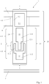
- Figure 1 shows a power device 1 having a source region 2 and a drain region 3, wherein a body region 4 and a drift region 6 are formed vertically in between.
- the body region 4 is p-doped
- the source region 2, the drain region 3 and the drift region 6 are n-doped, the drift region 6 with a lower doping concentration than the drain region three.
- the device 1 comprises a gate region 5 formed aside a channel region 4.1 of the body region 4.
- the gate region 5 comprises a gate electrode 5.1 and a gate dielectric 5.2, which capacitively couples the gate electrode 5.1 to the channel region 4.1.
- the device 1 comprises a field electrode 10 which is formed in a field electrode trench 7 extending into the drift region 6, namely into the semiconductor body 20.
- the gate electrode 5.1 is arranged above the field electrode 10 in the field electrode trench 7.
- the field electrode comprises a first field electrode structure 11 and a second field electrode structure 12 formed above.
- the first field electrode structure 11 is the lowermost one and the second field electrode structure 12 is the uppermost one, even though more than two field electrode structures 11, 12 can be stacked on each other as detailed below.
- the first field electrode structure 11 capacitively couples to a first section 6.1 of the drift region six
- the second field electrode structure 12 capacitively couples to a second section 6.2 of the drift region 6/thereof.
- the stacked field electrode structures 11, 12 can allow for a serial integration of lower voltage geometries, e. g. 60 V, which together support a higher voltage, e. g. 2 ⁇ 60 V in this example.
- a capacitive voltage divider e. g. with basically the same capacity between the field electrode structures 11, 12 and between the first field electrode structure 11 and the drain region 3
- the field electrode structures 11, 12 are formed with a vertical overlap 8 to increase their capacitive coupling.
- the vertical overlap 8 is formed between an upper overlap section 11.3 of the first field electrode structure 11 and a lower overlap section 12.1 of the second field electrode structure 12, wherein the upper overlap section 11.3 is arranged laterally outside of the lower overlap section, embracing the latter in the vertical cross-section shown.
- a coupling section 11.2 of the first field electrode structure 11 is formed below its upper overlap section 11.3, and a coupling section 12.2 of the second field electrode structure 12 is formed above its lower overlap section 12.1.
- the vertical overlap 8 increases the capacitive coupling between the field electrode structures 11, 12. This coupling could even become too large compared to the coupling to the drift region 6, e. g. if the vertical overlap 8 would extend over the whole height of the first field electrode structure. For that reason, the device 1 shown aims at balancing the respective coupling, in the example of figure 1 by a lateral displacement of the upper overlap section 11.3 towards the drift region.
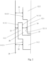
- Figure 2 shows an enlarged view of the field electrode structures 11, 12 and illustrates the lateral displacement in detail.
- the outer sidewall 11.3.1 of the upper overlap section 11.3 of the first field electrode structure 11 is offset laterally outwards.
- a first dielectric thickness 21 taken laterally between the upper overlap section 11.3 and the drift region 6 can be smaller than a second and/or third dielectric thickness 22, 23, the former taken between the drift region 6 and the coupling section 11.2, the latter between the drift region 6 and the coupling section 12.2.
- the first dielectric thickness 21 can be around only 20% of the second/third dielectric thickness 22, 23, e. g. 50 nm versus 300 nm. Moreover, the first dielectric thickness 21 can be smaller than a fourth dielectric thickness 24 taken between the overlap sections 11.3, 12.1. In particular, the fourth dielectric thickness 24 is taken between an inner sidewall 11.3.2 of the overlap section 11.3 and an outer sidewall 12.1.1 of the overlap section 12.1, the inner sidewall 11.3.2 facing away from the drift region 6, in contrast to the outer sidewalls 12.1.1, 11.3.1 and 11.2.1.
- a central upward facing face 27 of the first field electrode structure 11 is drawn as a straight line. However, it can have a sloped and/or curved shape, e. g. slope from both sides towards the center downwards and/or have a rounded edge at each side, namely at the transition into the inner sidewall 11.3.2, e. g. a convex edge rounding.
- Figure 3 illustrates a further embodiment with a field electrode 10 in a field electrode trench 7.
- the device as a whole can have the same set up as illustrated in figure 1 .
- field electrode structures 11, 12 are formed with a vertical overlap 8 to increase the capacitive coupling between the field electrode structures 11, 12.
- the coupling between the field electrode structures 11, 12 could become too large, if the vertical overlap 8 would extend over the whole height of the first field electrode structure 11.
- the coupling section 11.2 is in contrast formed with a vertical height 35 which is larger than the lateral width 36 of the overlap section 11.3.
- the first field electrode structure 11 is formed with a socket, so that the (vertical) layer thickness of the socket or bottom portion, namely of the coupling section 11.2, is larger than a lateral layer thickness of the overlap section 11.3.
- the vertical height 35 can be comparable to the vertical height 37 of the upper overlap section, e. g. be between 0.7-1.3 times the latter. Due to this geometry, the coupling between field electrode structures 11, 12 does not become too large, so that a dielectric layer 28 between the field electrode structures 11, 12 can be comparably small (no increased thickness required for counterbalancing).
- the fourth dielectric thickness 24 can even be smaller than the second and/or third dielectric thickness 22, 23.
- an outer wall face 38 of the second field electrode structure 12 extends with a step 39. Alternatively or in addition, it could extend obliquely, tilted with respect to the vertical and the horizontal direction 45, 46.
- a third field electrode structure 13 is arranged, having a lower overlap section 13.1, a coupling section 13.2 and, depending on whether a further field electrode structure (not shown) is arranged above, an upper overlap section 13.3.
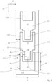
- Figure 4 also shows three stacked field electrode structures 11-13, which respectively have an upper overlap section 11.3-13.3 as discussed with reference to figures 1 and 2 .
- figure 4 illustrates a doping concentration 40 in the drift region 6.
- the doping concentration 40 which is shown on a logarithmic scale, has a gradient 41 in each of the sections 6.1-6.3.
- the doping concentration 40 is lower at the respective upper end and increases towards the respective lower end, for instance by around one order of magnitude.
- the doping concentration 40 decreases again, e. g. basically in a step function, the logarithmically plotted doping concentration 40 having for instance a sawtooth profile.
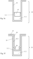
- Figures 5a-h illustrate several process steps for manufacturing field electrode structures as shown in figure 3 .
- the field electrode trench 7 has been etched into the semiconductor body 20, and the field dielectric 29 has been formed at the sidewall 7.1 of the field electrode trench 7.
- the field dielectric formation can for instance be a thermal oxidation, e. g. combined with a subsequent TEOS deposition.
- a field electrode structure material 61 has been deposited into the field electrode trench 7 to form a part of the first field electrode structure 11.
- the field electrode structure material 61 filled the trench 7 completely, and it has been etched back to fill only the bottom portion.
- the coupling section 11.2 of the first field electrode structure 11 is defined.
- a layer 60 of the field electrode structure material 61 is deposited, covering a frontside of the semiconductor body 20 and a preliminary field electrode trench sidewall 62.1. The latter is the inner sidewall of the field dielectric 29, which faces away from the drift region 6.
- a masking material 63 is deposited.
- the masking material 63 can for instance be a resist, e. g. photoresist. Initially, it fills the field electrode trench 7 completely, and it is etched back to arrive at the situation shown in figure 5d . There, it covers only a lower section 60.1 of the layer 60, while an upper section 60.2 is exposed. Subsequently, the field electrode structure material 61 is etched away in the upper section 60.2, for instance by wet etching or in particular dry etching. This etch step defines the upper overlap section 11.3 of the first field electrode structure.
- the masking material 63 has been removed, and a layer 66 of a dielectric material 65 has been deposited. It covers a frontside of the semiconductor body 20 and a preliminary field electrode trench sidewall 62.2. In this example, the latter is identical to the preliminary field electrode trench sidewall 62.1 discussed above with reference to figure 5c .
- a field electrode structure material 61 is deposited to fill the field electrode trench 7 completely. It is etched back subsequently to define the lower overlap section 12.1 of the second field electrode structure 12, namely to arrive at the structure shown in figure 5g .
- the layer 66 of the dielectric material 65 has been etched away to define a desired first dielectric thickness 21 for the coupling section 12.2 of the second field electrode structure 12.
- This coupling section 12.2 is formed by a further deposition of the field electrode structure material 61, as illustrated in figure 5h .
- the desired height of the coupling section 12.2 is defined.
- Figure 6 illustrates a process step that can be integrated between the steps shown in figures 5 b and c to manufacture an upper overlap section as illustrated in figures 1 / 2 and 4 .
- an additional etch step e. g. wet etching
- the field dielectric 29 is etched back from its initial thickness 70 to the first dielectric thickness 21, see figure 2 in comparison.
- the field electrode structure material can be deposited and etched back as shown in figures 5c-e to define the upper overlap section 11.3.
- the field dielectric 29 Prior to the formation of the coupling section 12.2 of the second field electrode structure as illustrated in figure 5h , the field dielectric 29 can be reinforced again, e. g. by TEOS deposition, to arrive at the desired third dielectric thickness shown in figure 2 .
- Figure 7 summarizes some of the processing steps in a flow diagram 80 after etching 81 the field electrode trench 7, the first field electrode structure 11 is formed 82. This can in particular comprise a formation 83 of the coupling section 11.2 and a subsequent formation 84 of the upper overlap section 11.3, as discussed above. Thereafter, the dielectric material 65 is deposited 85 to form the dielectric layer 28, see figure 5f . Subsequently, the second field electrode structure 12 is formed 86, e. g. by a subsequent formation of the lower overlap section 12.1, the coupling section 12.2 and the upper overlap section 12.3.
Landscapes
- Insulated Gate Type Field-Effect Transistor (AREA)
- Semiconductor Integrated Circuits (AREA)
- Electrodes Of Semiconductors (AREA)
Abstract
Description
- The present disclosure relates to a semiconductor power device with a channel region and a gate region.
- The gate region of the power device is formed aside the channel region, it comprises a gate dielectric and a gate electrode. The gate dielectric is arranged in between the channel region and the gate electrode, capacitively coupling the latter to the channel region. Vertically below the channel region, a drift region is formed, a field electrode trench extending into the latter. In this field electrode trench, a field electrode is arranged, capacitively coupling to the drift region.
- It is an object of the present application to provide a power device with improved characteristics, as well as a method of manufacturing such a device.
- This object is achieved by the power device of claim 1. Moreover, it is achieved by the method of
claim 13. The field electrode of this device comprises a first and a second field electrode structure, wherein the first field electrode structure couples to a first section of the drift region and the second field electrode structure couples to a second section thereof. In a vertical direction, the first section is arranged below the second section, namely on a greater vertical depth. The stacking of the field electrode structures in the field electrode trench can allow for an integration of a series of low-voltage geometries which together support a higher voltage. In consequence, the dependence of Ron • A of the breakdown voltage can, for example, be reduced, e. g. scale basically linearly whereas a device with only one field plate could for instance have an Ron • A depending essentially quadratically on the breakdown voltage. In other words, the stacked field electrode structures can allow for an Ron • A reduction while maintaining a certain breakdown voltage. - A biasing of the field electrode structures to a required voltage, e. g. to Vds/2 in case of two stacked field electrode structures, can for instance be achieved with a capacitive potential divider. E. g. during faster switching, the capacitors will bias the field electrode structures due to the current flowing through them. This requires the capacity between the field electrode structures to be adjusted to basically the same value as the capacity between the first field electrode structure and the drain region. However, if the field electrode structures would simply be stacked one on the other, the capacitive coupling would be too small due to the comparably small horizontal overlap, e. g. amount to only 20% of the capacity between the first field electrode structure and the drain region.
- To increase the capacitive coupling between the first and the second field electrode structure, they are formed with a vertical overlap. This means that a horizontal plane, which lies perpendicular to the vertical direction, intersects both field electrode structures. As discussed in detail below, this shall typically not imply that the vertical overlap is maximized, e. g. by nesting the second field electrode structure over the whole height of the first field electrode structure into the latter. Instead, in particular, the design of the first and the second field electrode structure can aim at a balancing of the coupling between the field electrode structures and between the field electrode and the drift region. If the capacitive coupling between the field electrode structures would become too large for geometrical reasons, a comparably thick dielectric, e. g. thick oxide, would be required in between, which could for example cause an increased mechanical stress in the field electrode trench, and/or could result in an unnecessarily wide trench.
- In general words, an approach of this application is to form a field electrode with a first and a second field electrode structure, the latter stacked on the former in the field electrode trench, wherein these field electrode structures are formed with a vertical overlap. In particular, as discussed in detail below, an additional means can be provided for increasing or adapting the capacitive coupling between the field electrode and the drift region. This can for example be the lateral displacement of an overlap section towards the drift region and/or an increased vertical height of a coupling section.
- Even though reference is primarily made to the first and the second field electrode structure, more than two field electrode structures can be stacked on each other in the field electrode trench. For the purpose of illustration, a 120 V device can for instance be fabricated from two 60 V devices stacked on each other, but it could also be fabricated from three 40 V devices stacked on each other, the latter resulting in an even lower Ron • A. In general words, in case of n field electrode structures stacked on each other in the trench, a target can be to bias each field electrode structure to Vds/n.
- Particular embodiments and features are presented throughout this disclosure and in particular in the dependent claims. Thereby, the individual features shall be disclosed independently of a specific claim category, the disclosure relates to apparatus and device aspects, but also to method and use aspects. If for instance a device manufactured in a specific way is described, this is also a disclosure of a respective manufacturing process, and vice versa.
- The gate region, which comprises a gate dielectric and a gate electrode, can particularly be formed laterally aside the channel region, e. g. in a trench. In particular, the gate electrode can be arranged in the field electrode trench, namely vertically above the uppermost field electrode structure, e. g. electrically isolated therefrom by an insulating layer. In a lateral direction, the field electrode trench can have a longitudinal extension, it can for instance form a grid-like or in particular stripe-like pattern together with other respective trenches, when seen in a top view. In the trench, in particular seen in a vertical cross section through the trench, the field electrode structures among each other and/or the field electrode structures and the gate electrode are electrically isolated from each other by a respective layer or layers of an insulating material. Between two neighboring trenches, the drift region can in particular have a continuous extension, so that for instance no further compensation structure is formed there.
- Generally, when reference to a "vertical cross-section" is made, the cross-sectional plane lies parallel to the vertical direction. The sectional plane can intersect the trench perpendicularly to its longitudinal extension in a lateral direction, e. g. lie perpendicular to the stripes of an aforementioned stripe-design. Generally, the "vertical direction" lies perpendicular to a surface of the device, for instance a surface of the semiconductor body or of a frontside metallization. Independently of the number of field electrode structures stacked and/or of whether the gate electrode is arranged in the trench, the field electrode is electrically isolated from the drift region by a field dielectric. This field dielectric can in particular electrically isolate the lowermost field electrode structure in the trench from the drift region and also from the drain region, e. g. at least in the active region of the device.
- Referring to a source and a drain region of a first conductivity type, the channel region can be formed in a body region of a second conductivity type opposite to the first conductivity type. In particular, the source region can be formed at a frontside of the device and the drain region at a backside thereof, the channel region and the drift region arranged vertically between, e. g. the drift region between the channel region and the drain region. The drift region can be of the first conductivity type as well, wherein its dopant concentration is lower compared to the drain region. As a power device, such a transistor can for instance have a breakdown voltage of at least 10 V, 20 V, 30 V, 40 V or 50 V, possible upper limits being for example not more than 800 V, 600 V, 400 V or 200 V.
- In an embodiment, an upper overlap section of the first field electrode structure is arranged laterally outside a lower overlap section of the second field electrode structure, namely laterally between the lower overlap section and the drift region. In particular, the upper overlap section can be displaced towards the drift region, an outer sidewall of the upper overlap section being offset laterally outwards compared to an outer sidewall of a coupling section of the second field electrode structure. In other words, the outer sidewalls of the upper overlap section and coupling section do not lie flush with respect to a vertical plane, the upper overlap section sidewall being laterally closer to the drift region. This can allow for the aforementioned balancing of the coupling between the first field electrode structure and the drift region and between the first and the second field electrode structure. Consequently, e. g. the balance of the capacitive potential divider can be improved. The capacitor formed by the upper overlap section can be required to support only a small potential difference, e. g. a few volts, between the first field electrode structure and drift region. Consequently, a standard dielectric material can be used, for instance oxide, and/or only one field oxide thickness is required (e. g. around 300 nm). Generally, an "outer" sidewall of a field electrode structure is a sidewall facing towards the drift region, wherein an "inner" sidewall faces away from the drift region.
- In an embodiment, an outer sidewall of the upper overlap section of the first field electrode structure is offset laterally outwards compared to an outer sidewall of a coupling section of the first field electrode structure. In other words, the outer sidewall of the first field electrode structure is closer to the drift region in an overlap section than in a coupling section of the first field electrode structure. The coupling section of the first field electrode structure is arranged at a greater vertical depth than its overlap section. In this embodiment, the first field electrode structure can in particular be the lowermost field electrode structure in the trench, the coupling section coupling solely to the drift region, not to a further field electrode structure. In combination with the embodiment described above, the outer sidewall can be closer to the drift region in the overlap section than in a coupling section below (of the first field electrode structure) and the coupling section above (of the second field electrode structure).
- In an embodiment, a first dielectric thickness, which is taken laterally between the upper overlap section of the first field electrode structure and the drift region is smaller than
- a second dielectric thickness taken laterally between a coupling section of the first field electrode structure and the drift region, and/or
- a third dielectric thickness taken laterally between a coupling section of the second field electrode structure and the drift region, and/or
- a fourth dielectric thickness taken laterally between the upper overlap section of the first field electrode structure and the lower overlap section of the second field electrode structure.
- In case that a respective lateral distance varies along the vertical extension of the respective section, a mean value taken over the vertical extension of the respective section is considered. Particularly, however, the first and/or second and/or third and/or fourth dielectric thickness can be constant over the respective section.
- In an embodiment, which can be combined with or be an alternative to the lateral displacement of the outer sidewall discussed above, a vertical height of the coupling section of the first field electrode structure is larger than the lateral width of its upper overlap section. In other words, a (vertical) thickness of a layer forming the coupling section is larger than the (lateral) thickness of a layer forming the upper overlap section. The vertical height or vertical layer thickness can for instance be at least 2 times, 3 times or 4 times larger than the lateral width or lateral layer thickness, wherein possible upper limits can for instance be not more than 20 times, 15 times or 10 times.
- As discussed above, the coupling section of the first field electrode structure is formed on a smaller vertical height than its overlap section, namely arranged at a greater depth. This shall not imply that the coupling section has a smaller vertical extension than the overlap section, which is possible, but not mandatory. Generally, in its overlap section, a respective field electrode structure capacitively couples to another field electrode structure. Additionally, this overlap section, in particular upper overlap section, can also capacitively couple to the drift region, e.g. couple laterally outwards to the drift region and laterally inwards to the overlap section of the other field electrode structure. In contrast to an overlap section, a respective coupling section of a respective field electrode structure can couple solely to the drift region in the lateral direction. A horizontal plane through the coupling section intersects for instance solely the respective field electrode structure, e.g. no other field electrode structure being intersected by the horizontal plane.
- As discussed above, more than two field electrode structures can be stacked in the field electrode trench, wherein the "first" field electrode structure is not necessarily the lowermost field electrode structure in the trench. Below, a further field electrode structure can be arranged, which can in particular have a vertical overlap with the first field electrode structure. In this example, an upper overlap section of the further field electrode structure, which forms the vertical overlap with the first field electrode structure, can be formed above a coupling section of the further field electrode structure. Alternatively, however, the first field electrode structure can also be the lowermost one in the trench.
- In an embodiment, the coupling section of the first field electrode structure has a vertical height which is at least 0.2 times the vertical height of the upper overlap section of the first field electrode structure. Further possible lower limits are 0.3 times, 0.4 times, 0.5 times, 0.6 times or 0.7 times the vertical height of the upper overlap section. Independently of these lower limits, the vertical height of the coupling section can be not more than 10 times, 8 times, 6 times, 4 times, 3 times, 2 times, 1.8 times, 1.7 times, 1.6 times, 1.5 times, 1.4 times or 1.3 times the vertical height of the upper overlap section.
- In an embodiment, a fourth dielectric thickness, which is taken laterally between the upper overlap section of the first field electrode structure and the lower overlap section of the second field electrode structure, is smaller than a second dielectric thickness taken laterally between the coupling section of the first field electrode structure and the drift region. The fourth dielectric thickness can for instance be 1.2 µm at maximum, in particular 1 µm, 0.8 µm, 0.6 µm, 0.5 µm or 0.4 µm at maximum. Possible lower limits are 0.05 µm, 0.1 µm or 0.2 µm at minimum, wherein these absolute values can also depend from the voltage class.
- In an embodiment, an outer wall face of the second field electrode structure has an oblique and/or stepped extension in a transition section of the second field electrode structure. This transition section is arranged vertically between the lower overlap section and the coupling section of the second field electrode structure, and the oblique/stepped shape can for instance result from an advantageous method of manufacturing, see in detail below. In this respect, "obliquely" means tilted with respect to the vertical and the lateral direction, namely neither parallel nor perpendicular to one of them. Due to the "stepped" design, an edge can be formed between a horizontal and a vertical subsection of the transition section.
- In an embodiment, the doping concentration in the drift region has a gradient in the first section, to which the first field electrode structure capacitively couples, and/or in the second section, to which the second field electrode structure capacitively couples. If more than two field electrode structures are stacked in the trench, the doping concentration can have a gradient in more than two sections of the drift region, it can in particular have a gradient in each section of the drift region, to which a respective field electrode structure couples. Independently of these details, the doping concentration can in particular be lower at the upper end of a respective coupling section than at the lower and thereof. In a vertical direction downwards, the doping concentration can increase within a respective section of the drift region, and it can decrease between two respective sections, e. g. basically stepwise. In other words, the doping concentration can basically follow a sawtooth-profile. In general, however, a constant doping profile can also be provided.
- In an embodiment, a dielectric layer arranged between the first and the second field electrode structure is made of another dielectric material than a field dielectric formed between the field electrode and the drift region. The upper overlap section of the first field electrode structure and the lower overlap section of the second field electrode structure can be capacitively coupled via the dielectric layer. The dielectric material of this dielectric layer can in particular have another dielectric constant than the field dielectric material, which can offer a (further) possibility to adjust or balance the capacitive coupling between the field electrode structures compared to the coupling to the drift region. By way of example, the field dielectric material can be silicon oxide, wherein silicon nitride having around twice the dielectric constant can be chosen for the dielectric layer.
- In an embodiment, the capacity between the first and the second field electrode structure is set to the capacity between the first field electrode structure and the drain region. In other words, these capacities can have basically the same value. If a third field electrode structure is stacked on the second one, the capacity value between these can in particular be set to the capacity value between the first and the second field electrode structure. In other words, if at least three field electrode structures are stacked, the at least two capacities formed in this chain can in particular have the same value. As discussed above, this can for instance bias the field electrode structures at basically the same voltage values, in particular during faster switching.
- In an embodiment, the device comprises a resistor connected in parallel with the capacitor formed by the first and the second field electrode structure. If more than two field electrode structures are stacked, a chain of capacitors being formed, a respective resistor can be connected in parallel with each of the capacitors, wherein these capacitor/resistor pairs can be connected in series. With this RC-coupling, the desired voltage drop can be achieved during static or slow switching operation (resistive voltage divider) and during faster switching (capacitive potential divider). In general, and external resistor or resistors are conceivable, particularly it or they can be integrated into the semiconductor body.
- The method of manufacturing the power device can comprise
- i) etching the field electrode trench;
- ii) forming the first field electrode structure;
- iii) depositing a dielectric material to form a dielectric layer;
- iv) forming the second field electrode structure
- Depending on the total number of field electrode structures to be formed in the trench, the dielectric layer formation (step iii) and the field electrode structure formation (step iv) can be repeated accordingly. Independently of the total number of field electrode structures formed in the trench, the gate electrode can be formed after and above the uppermost field electrode structure in the field electrode trench, which will also depend on the specific device design, as discussed above.
- Forming a field electrode structure with a coupling section and an overlap section below and/or an overlap section above will typically require a plurality subsequent processing steps, the different sections formed one after the other. In an embodiment, for forming the upper overlap section of a respective field electrode structure, a layer of a field electrode structure material is deposited onto a preliminary field electrode trench sidewall. This preliminary trench sidewall can for instance be the inner sidewall of a field dielectric deposited onto and/or formed on or at the initial trench sidewall resulting after the trench etch (as discussed above, the inner sidewall faces away from the drift region). With the deposition of the field electrode structure material, e. g. doped polysilicon, a layer of the field electrode structure material is formed on the preliminary field electrode trench sidewall.
- Subsequently, a masking material is deposited to cover a lower section of this layer e. g. a resist fill. The masking material can initially fill the trench completely and can be etched back to cover only the lower section of the field electrode structure material layer and, vice versa, to expose an upper section thereof. When the lower section of the field electrode structure material is protected by the masking material, the upper section can be etched away, for instance by dry etching, e. g. isotropic silicon dry etch, or by wet etching. After this etch step, the upper overlap section of the respective field electrode structure remains, and the masking material can be removed, e. g. the resist be stripped.
- To manufacture an aforementioned device with the sidewall of the field electrode being offset towards the drift region in the upper overlap section, e. g. compared to the sidewall of the coupling section below and/or above, a further etch step can be introduced prior to the deposition of the field electrode structure material layer onto the preliminary trench sidewall. With this etch step, the thickness of the field dielectric layer formed at/deposited onto the initial trench sidewall can be reduced, for instance by at least 20% or 30%, possible upper limits being for example not more than 80% or 70%. The field dielectric thickness can for instance be reduced by wet etching. In the coupling section of the respective field electrode structure, namely below the overlap section, the initial field dielectric thickness will remain, the inner sidewall of the field dielectric being protected by the field electrode structure material forming the coupling section of the respective field electrode structure. After forming the overlap section of the respective field electrode structure in the way described above and prior to forming the coupling section of the subsequent field electrode structure, the field dielectric thickness can be increased again, e. g. by an oxide deposition.
- Prior to forming the upper overlap section of the respective field electrode structure, its coupling section can be formed. For that purpose, the field electrode structure material can be deposited into the trench to fill the respective section completely, e. g. continuously between two opposite preliminary field electrode trench sidewalls. This can for instance be achieved by a complete fill of the trench with the field electrode structure material in combination with a subsequent etch back to adjust the desired height of the coupling section. After the formation of the upper overlap section of the respective field electrode structure, a layer of a dielectric material can be deposited to form the dielectric between the respective field electrode structure and the subsequent field electrode structure, the lower overlap section of the subsequent field electrode structure can be formed by a deposition of field electrode structure material.
- In an embodiment, a layer of dielectric material, which is deposited onto the preliminary trench sidewall when the dielectric layer between two respective field electrode structures is formed, is etched away subsequently. In particular, it can be etched away after field electrode structure material has been deposited to form the lower overlap section of the second or generally subsequent field electrode structure. In consequence, the outer wall face of the second or subsequent field electrode structure can have the oblique and/or stepped shape in the transition region, as discussed above. With this etch step, the dielectric thickness between the coupling section of the second or subsequent field electrode structure and the drift region can be adjusted independently of the dielectric layer thickness between the field electrode structures.
- Parts of the application can be summarized by the following aspects:
- 1st aspect: A power device, having
- a channel region,
- a gate region formed aside the channel region, for controlling a channel formation,
- a drift region formed vertically below the channel region,
- a field electrode formed in a field electrode trench extending vertically into the drift region,
- wherein the field electrode comprises a first and a second field electrode structure, the first field electrode structure capacitively coupling to a first section of the drift region and the second field electrode structure capacitively coupling to a second section of the drift region, arranged vertically above the first section,
- the first and the second field electrode structure formed with a vertical overlap and adapted to balance a capacitive coupling between the first and the second field electrode structure and between the field electrode and the drift region.
- 2nd aspect: The power device of the 1st aspect, an upper overlap section of the first field electrode structure arranged laterally outside a lower overlap section of the second field electrode structure, wherein, seen in a vertical cross-section, an outer sidewall of the upper overlap section is offset laterally outwards compared to an outer sidewall of a coupling section of the second field electrode structure, which coupling section is formed on a larger vertical height than the lower overlap section.
- 3rd aspect: The power device of the 1st or 2nd aspect, an upper overlap section of the first field electrode structure arranged laterally outside a lower overlap section of the second field electrode structure, wherein, seen in a vertical cross-section, an outer sidewall of the upper overlap section is offset laterally outwards compared to an outer sidewall of a coupling section of the first field electrode structure, which coupling section is formed on smaller vertical height than the upper overlap section.
- 4th aspect: The power device of any one of the preceding aspects, an upper overlap section of the first field electrode structure arranged laterally outside a lower overlap section of the second field electrode structure, wherein a first dielectric thickness taken laterally between the upper overlap section and the drift region is smaller than at least one of
- a second dielectric thickness taken laterally between a coupling section of the first field electrode structure and the drift region, and
- a third dielectric thickness taken laterally between a coupling section of the second field electrode structure and the drift region, and
- a fourth dielectric thickness taken laterally between the upper overlap section of the first field electrode structure and the lower overlap section of the second field electrode structure.
- 5th aspect: The power device of any one of the preceding aspects, an upper overlap section of the first field electrode structure arranged laterally outside a lower overlap section of the second field electrode structure, wherein, seen in a vertical cross-section, a vertical height of a coupling section of the first field electrode structure is larger than a lateral width of the upper overlap section, the coupling section formed on smaller vertical height than the upper overlap section.
- 6th aspect: The power device of any one of the preceding aspects, an upper overlap section of the first field electrode structure arranged laterally outside a lower overlap section of the second field electrode structure and a coupling section of the first field electrode structure formed on a smaller vertical height than the upper overlap section, wherein the coupling section has a vertical height which is between 0.2 - 10 times the vertical height of the upper overlap section.
- 7th aspect: The power device of any one of the preceding aspects, an upper overlap section of the first field electrode structure arranged laterally outside a lower overlap section of the second field electrode structure, wherein a fourth dielectric thickness taken laterally between the upper overlap section and the lower overlap section is smaller than a second dielectric thickness taken laterally between a coupling section of the first field electrode structure and the drift region.
- 8th aspect: The power device of any one of the preceding aspects, an upper overlap section of the first field electrode structure arranged laterally outside a lower overlap section of the second field electrode structure and a coupling section of the second field electrode structure formed on a larger vertical height than the lower overlap section, wherein, seen in a vertical cross-section, an outer wall face of the second field electrode structure extends between the lower overlap section and the coupling section at least one of obliquely and with a step.
- 9th aspect: The power device of any one of the preceding aspects, wherein a doping concentration in the drift region has a gradient in at least one of the first section of the drift region and the second section of the drift region.
- 10th aspect: The power device of any one of the preceding aspects, wherein a dielectric layer, which is arranged between the first and the second field electrode structure where the vertical overlap is formed, is made of a dielectric material other than a field dielectric formed between the field electrode and the drift region.
- 11th aspect: The power device of any one of the preceding aspects, wherein a capacity value between the first and the second field electrode structure is set to a capacity value between the first field electrode structure and a drain region.
- 12th aspect: The power device of any one of the preceding aspects, comprising a resistor connected in parallel with a capacitor formed by the first and the second field electrode structure.
- 13th aspect: A method of manufacturing the power device of any one of the preceding aspects, comprising
- i) etching the field electrode trench;
- ii) forming the first field electrode structure;
- iii)depositing a dielectric material to form a dielectric layer;
- iv)forming the second field electrode structure.
- 14th aspect: The method of
aspect 13, wherein, for forming an upper overlap section of the first field electrode structure, a layer of a field electrode structure material is deposited onto a preliminary field electrode trench sidewall, a masking material being deposited thereafter to cover a lower section of the layer of the field electrode structure material while an upper section of the layer of the field electrode structure material is etched away subsequently. - 15th aspect: The method of
aspect 13 or 14, wherein, while the dielectric material is deposited in step iii), a layer of the dielectric material is deposited onto a preliminary field electrode trench sidewall, the layer being etched away subsequently, namely after a field electrode structure material has been deposited to form a lower overlap section of the second field electrode structure. - Below, the power device and the manufacturing of the same are explained in further detail by means of exemplary embodiments. Therein, the individual features can also be relevant in a different combination.
- Figure 1
- shows a power device with two field electrode structures, illustrating a vertical overlap and lateral sidewall displacement in the overlap section;
- figure 2
- shows a detailed view of the field electrode structures of
figure 1 ; - figure 3
- illustrates stacked field electrode structures of another device, illustrating a vertical overlap and an increased coupling section height;
- figure 4
- illustrates field electrode structures comparable to those of
figures 1 and2 and illustrates a doping concentration gradient in the drift region; - figures 5a-h
- illustrate some processing steps for manufacturing the field electrode structures of
figure 3 ; - figure 6
- illustrates some processing steps for manufacturing the field electrode structures of
figures 1 and2 or4 ; - figure 7
- shows a flow diagram summarizing some processing steps for manufacturing a power device disclosed here.
-
Figure 1 shows a power device 1 having asource region 2 and adrain region 3, wherein abody region 4 and adrift region 6 are formed vertically in between. In the example shown, thebody region 4 is p-doped, whereas thesource region 2, thedrain region 3 and thedrift region 6 are n-doped, thedrift region 6 with a lower doping concentration than the drain region three. Moreover, the device 1 comprises agate region 5 formed aside a channel region 4.1 of thebody region 4. Thegate region 5 comprises a gate electrode 5.1 and a gate dielectric 5.2, which capacitively couples the gate electrode 5.1 to the channel region 4.1. By applying a voltage to the gate electrode 5.1, a channel formation and vertical current flow through the channel region 4.1 and, in consequence, between asource region 2 and adrain region 3 can be controlled. - In addition, the device 1 comprises a
field electrode 10 which is formed in afield electrode trench 7 extending into thedrift region 6, namely into thesemiconductor body 20. In the example shown, the gate electrode 5.1 is arranged above thefield electrode 10 in thefield electrode trench 7. The field electrode comprises a firstfield electrode structure 11 and a secondfield electrode structure 12 formed above. In the example shown, the firstfield electrode structure 11 is the lowermost one and the secondfield electrode structure 12 is the uppermost one, even though more than twofield electrode structures - Via a
field dielectric 29, the firstfield electrode structure 11 capacitively couples to a first section 6.1 of the drift region six, and the secondfield electrode structure 12 capacitively couples to a second section 6.2 of thedrift region 6/thereof. As discussed in the general description in detail, the stackedfield electrode structures field electrode structures field electrode structure 11 and thedrain region 3, thefield electrode structures vertical overlap 8 to increase their capacitive coupling. Thevertical overlap 8 is formed between an upper overlap section 11.3 of the firstfield electrode structure 11 and a lower overlap section 12.1 of the secondfield electrode structure 12, wherein the upper overlap section 11.3 is arranged laterally outside of the lower overlap section, embracing the latter in the vertical cross-section shown. A coupling section 11.2 of the firstfield electrode structure 11 is formed below its upper overlap section 11.3, and a coupling section 12.2 of the secondfield electrode structure 12 is formed above its lower overlap section 12.1. - The
vertical overlap 8 increases the capacitive coupling between thefield electrode structures drift region 6, e. g. if thevertical overlap 8 would extend over the whole height of the first field electrode structure. For that reason, the device 1 shown aims at balancing the respective coupling, in the example offigure 1 by a lateral displacement of the upper overlap section 11.3 towards the drift region. -
Figure 2 shows an enlarged view of thefield electrode structures field electrode structure 12 and an outer sidewall 11.2.1 of the coupling section 11.2 of the firstfield electrode structure 11, the outer sidewall 11.3.1 of the upper overlap section 11.3 of the firstfield electrode structure 11 is offset laterally outwards. Afirst dielectric thickness 21 taken laterally between the upper overlap section 11.3 and thedrift region 6 can be smaller than a second and/or thirddielectric thickness drift region 6 and the coupling section 11.2, the latter between thedrift region 6 and the coupling section 12.2. - By way of example, the
first dielectric thickness 21 can be around only 20% of the second/third dielectric thickness first dielectric thickness 21 can be smaller than afourth dielectric thickness 24 taken between the overlap sections 11.3, 12.1. In particular, thefourth dielectric thickness 24 is taken between an inner sidewall 11.3.2 of the overlap section 11.3 and an outer sidewall 12.1.1 of the overlap section 12.1, the inner sidewall 11.3.2 facing away from thedrift region 6, in contrast to the outer sidewalls 12.1.1, 11.3.1 and 11.2.1. In this drawing, a central upward facingface 27 of the firstfield electrode structure 11 is drawn as a straight line. However, it can have a sloped and/or curved shape, e. g. slope from both sides towards the center downwards and/or have a rounded edge at each side, namely at the transition into the inner sidewall 11.3.2, e. g. a convex edge rounding. -
Figure 3 illustrates a further embodiment with afield electrode 10 in afield electrode trench 7. Apart from the specific differences discussed below, the device as a whole can have the same set up as illustrated infigure 1 . As discussed above,field electrode structures vertical overlap 8 to increase the capacitive coupling between thefield electrode structures field electrode structures vertical overlap 8 would extend over the whole height of the firstfield electrode structure 11. This would be the case, if a bottom portion of the firstfield electrode structure 11 would have, taken in avertical direction 45, basically the same thickness as the upper overlap section 11.3 has in alateral direction 46, which could result from a deposition of the bottom portion and the upper overlap section 11.3 as a layer in the same process step. - In
figure 3 , the coupling section 11.2 is in contrast formed with avertical height 35 which is larger than thelateral width 36 of the overlap section 11.3. In other words, the firstfield electrode structure 11 is formed with a socket, so that the (vertical) layer thickness of the socket or bottom portion, namely of the coupling section 11.2, is larger than a lateral layer thickness of the overlap section 11.3. By increasing thevertical height 35 of the coupling section 11.2, the coupling to thedrift region 6, and in particular to thedrain region 3 can be adjusted, e. g. independently of the coupling between thefield electrode structures - Depending on the design in detail, the
vertical height 35 can be comparable to thevertical height 37 of the upper overlap section, e. g. be between 0.7-1.3 times the latter. Due to this geometry, the coupling betweenfield electrode structures dielectric layer 28 between thefield electrode structures fourth dielectric thickness 24 can even be smaller than the second and/or thirddielectric thickness - Between the lower overlap section 12.1 and the coupling section 12.2, an outer wall face 38 of the second
field electrode structure 12 extends with astep 39. Alternatively or in addition, it could extend obliquely, tilted with respect to the vertical and thehorizontal direction field electrode structure 12, a thirdfield electrode structure 13 is arranged, having a lower overlap section 13.1, a coupling section 13.2 and, depending on whether a further field electrode structure (not shown) is arranged above, an upper overlap section 13.3. -
Figure 4 also shows three stacked field electrode structures 11-13, which respectively have an upper overlap section 11.3-13.3 as discussed with reference tofigures 1 and2 . In addition,figure 4 illustrates adoping concentration 40 in thedrift region 6. Thedoping concentration 40, which is shown on a logarithmic scale, has agradient 41 in each of the sections 6.1-6.3. For each of the field electrode structures 11-13 or sections 6.1-6.3, thedoping concentration 40 is lower at the respective upper end and increases towards the respective lower end, for instance by around one order of magnitude. Between two sections 6.1-6.3, thedoping concentration 40 decreases again, e. g. basically in a step function, the logarithmically plotteddoping concentration 40 having for instance a sawtooth profile. -
Figures 5a-h illustrate several process steps for manufacturing field electrode structures as shown infigure 3 . Infigure 5a , thefield electrode trench 7 has been etched into thesemiconductor body 20, and thefield dielectric 29 has been formed at the sidewall 7.1 of thefield electrode trench 7. The field dielectric formation can for instance be a thermal oxidation, e. g. combined with a subsequent TEOS deposition. - In
figure 5b , a fieldelectrode structure material 61 has been deposited into thefield electrode trench 7 to form a part of the firstfield electrode structure 11. In detail, prior to the situation shown infigure 5B , the fieldelectrode structure material 61 filled thetrench 7 completely, and it has been etched back to fill only the bottom portion. Likewise, the coupling section 11.2 of the firstfield electrode structure 11 is defined. After this etch back step, a layer 60 of the fieldelectrode structure material 61 is deposited, covering a frontside of thesemiconductor body 20 and a preliminary field electrode trench sidewall 62.1. The latter is the inner sidewall of thefield dielectric 29, which faces away from thedrift region 6. - Subsequently, a masking
material 63 is deposited. The maskingmaterial 63 can for instance be a resist, e. g. photoresist. Initially, it fills thefield electrode trench 7 completely, and it is etched back to arrive at the situation shown infigure 5d . There, it covers only a lower section 60.1 of the layer 60, while an upper section 60.2 is exposed. Subsequently, the fieldelectrode structure material 61 is etched away in the upper section 60.2, for instance by wet etching or in particular dry etching. This etch step defines the upper overlap section 11.3 of the first field electrode structure. - In
figure 5f , the maskingmaterial 63 has been removed, and alayer 66 of adielectric material 65 has been deposited. It covers a frontside of thesemiconductor body 20 and a preliminary field electrode trench sidewall 62.2. In this example, the latter is identical to the preliminary field electrode trench sidewall 62.1 discussed above with reference tofigure 5c . After the dielectric material deposition, again, a fieldelectrode structure material 61 is deposited to fill thefield electrode trench 7 completely. It is etched back subsequently to define the lower overlap section 12.1 of the secondfield electrode structure 12, namely to arrive at the structure shown infigure 5g . There, in addition, thelayer 66 of thedielectric material 65 has been etched away to define a desiredfirst dielectric thickness 21 for the coupling section 12.2 of the secondfield electrode structure 12. This coupling section 12.2 is formed by a further deposition of the fieldelectrode structure material 61, as illustrated infigure 5h . In a subsequent etch back step, the desired height of the coupling section 12.2 is defined. -
Figure 6 illustrates a process step that can be integrated between the steps shown infigures 5 b andc to manufacture an upper overlap section as illustrated infigures 1 /2 and4 . With an additional etch step, e. g. wet etching, thefield dielectric 29 is etched back from itsinitial thickness 70 to thefirst dielectric thickness 21, seefigure 2 in comparison. Subsequently, the field electrode structure material can be deposited and etched back as shown infigures 5c-e to define the upper overlap section 11.3. Prior to the formation of the coupling section 12.2 of the second field electrode structure as illustrated infigure 5h , thefield dielectric 29 can be reinforced again, e. g. by TEOS deposition, to arrive at the desired third dielectric thickness shown infigure 2 . -
Figure 7 summarizes some of the processing steps in a flow diagram 80 after etching 81 thefield electrode trench 7, the firstfield electrode structure 11 is formed 82. This can in particular comprise aformation 83 of the coupling section 11.2 and asubsequent formation 84 of the upper overlap section 11.3, as discussed above. Thereafter, thedielectric material 65 is deposited 85 to form thedielectric layer 28, seefigure 5f . Subsequently, the secondfield electrode structure 12 is formed 86, e. g. by a subsequent formation of the lower overlap section 12.1, the coupling section 12.2 and the upper overlap section 12.3.
Claims (15)
- A power device (1), comprising:a channel region (4.1);a gate region (5) formed aside the channel region (4.1), for controlling a channel formation;a drift region (6) formed vertically below the channel region (4.1); anda field electrode (10) formed in a field electrode trench (7) extending vertically into the drift region (6), wherein the field electrode (10) comprises a first field electrode structure (11) and a second field electrode structure (12),wherein the first field electrode structure (11) comprises an upper overlap section (11.3) and a coupling section (11.2),wherein the second field electrode structure (12) comprises a lower overlap section (12.1),wherein the upper overlap section (11.3) of the first field electrode structure (11) is arranged laterally outside the lower overlap section (12.1) of the second field electrode structure (12),wherein a first dielectric thickness (21) taken laterally between the upper overlap section (11.3) and the drift region (6) is smaller than a second dielectric thickness (22) taken laterally between the coupling section (11.2) of the first field electrode structure (11) and the drift region (6).
- The power device (1) of claim 1, wherein, seen in a vertical cross-section, an outer sidewall (11.3.1) of the upper overlap section (11.3) is offset laterally outwards compared to an outer sidewall (12.2.1) of a coupling section (12.2) of the second field electrode structure (12), which coupling section (12.2) is formed on a larger vertical height than the lower overlap section (12.1).
- The power device (1) of claim 1 or 2, wherein, seen in a vertical cross-section, an outer sidewall (11.3.1) of the upper overlap section (11.3) is offset laterally outwards compared to an outer sidewall (11.2.1) of a coupling section (11.2) of the first field electrode structure (11), which coupling section (11.2) is formed on smaller vertical height than the upper overlap section (11.3).
- The power device (1) of any one of the preceding claims, wherein the first dielectric thickness (21) is smaller than a third dielectric thickness (23) taken laterally between a coupling section (12.2) of the second field electrode structure (12) and the drift region (6).
- The power device (1) of any one of the preceding claims, wherein, seen in a vertical cross-section, an outer wall face (38) of the second field electrode structure (12) has an oblique extension.
- The power device (1) of any one of the preceding claims, wherein, seen in a vertical cross-section, an outer wall face (38) of the second field electrode structure (12) extends with a step (39).
- The power device (1) of claim 6, wherein the step (39) forms an edge between a horizontal and a vertical subsection.
- The power device (1) of any one of the preceding claims, wherein the first dielectric thickness (21) varies along the vertical extension of the upper overlap section (11.3) and/or the second dielectric thickness (22) varies along the vertical extension of the coupling section (11.2).
- The power device (1) of any one of the preceding claims, wherein a first dielectric thickness taken laterally between an upper overlap section (12.3) of the second field electrode structure (12) and the drift region (6) is smaller than a second dielectric thickness taken laterally between a coupling section (12.2) of the second field electrode structure (12) and the drift region (6). [page 14, lines 16/17]
- The power device (1) of any one of the preceding claims, wherein a doping concentration (40) in the drift region (6) has a gradient (41).
- The power device (1) of any one of the preceding claims, wherein a capacity value between the first and the second field electrode structure (11,12) is set to a capacity value between the first field electrode structure (11) and a drain region (3).
- The power device (1) of any one of the preceding claims, comprising a resistor connected in parallel with a capacitor formed by the first and the second field electrode structure (11,12).
- A method of manufacturing the power device (1) of any one of the preceding claims, comprisingi) etching (81) the field electrode trench (7);ii) forming the first field electrode structure (11);iii) depositing a dielectric material (65) to form a dielectric layer (28);iv) forming the second field electrode structure (12).
- The method of claim 13, wherein, for forming the upper overlap section (11.3) of the first field electrode structure (11), a layer (60) of a field electrode structure material (61) is deposited onto a preliminary field electrode trench sidewall (62.1), a masking material (63) being deposited thereafter to cover a lower section (60.1) of the layer (60) of the field electrode structure material (61) while an upper section (60.2) of the layer (60) of the field electrode structure material (61) is etched away subsequently.
- The method of claim 13 or 14, wherein, while the dielectric material (65) is deposited in step iii), a layer (66) of the dielectric material (65) is deposited onto a preliminary field electrode trench sidewall (62.2), the layer (66) being etched away subsequently, namely after a field electrode structure material (61) has been deposited to form a lower overlap section (12.1) of the second field electrode structure (12).
Priority Applications (1)
| Application Number | Priority Date | Filing Date | Title |
|---|---|---|---|
| EP23181788.3A EP4235753A3 (en) | 2021-02-17 | 2021-02-17 | Semiconductor power device and method of manufacturing the same |
Applications Claiming Priority (2)
| Application Number | Priority Date | Filing Date | Title |
|---|---|---|---|
| EP21157608.7A EP4047665A1 (en) | 2021-02-17 | 2021-02-17 | Semiconductor power device and method of manufacturing the same |
| EP23181788.3A EP4235753A3 (en) | 2021-02-17 | 2021-02-17 | Semiconductor power device and method of manufacturing the same |
Related Parent Applications (1)
| Application Number | Title | Priority Date | Filing Date |
|---|---|---|---|
| EP21157608.7A Division EP4047665A1 (en) | 2021-02-17 | 2021-02-17 | Semiconductor power device and method of manufacturing the same |
Publications (2)
| Publication Number | Publication Date |
|---|---|
| EP4235753A2 true EP4235753A2 (en) | 2023-08-30 |
| EP4235753A3 EP4235753A3 (en) | 2023-11-08 |
Family
ID=74666578
Family Applications (2)
| Application Number | Title | Priority Date | Filing Date |
|---|---|---|---|
| EP23181788.3A Pending EP4235753A3 (en) | 2021-02-17 | 2021-02-17 | Semiconductor power device and method of manufacturing the same |
| EP21157608.7A Pending EP4047665A1 (en) | 2021-02-17 | 2021-02-17 | Semiconductor power device and method of manufacturing the same |
Family Applications After (1)
| Application Number | Title | Priority Date | Filing Date |
|---|---|---|---|
| EP21157608.7A Pending EP4047665A1 (en) | 2021-02-17 | 2021-02-17 | Semiconductor power device and method of manufacturing the same |
Country Status (4)
| Country | Link |
|---|---|
| US (2) | US12557333B2 (en) |
| EP (2) | EP4235753A3 (en) |
| KR (1) | KR102993662B1 (en) |
| CN (1) | CN114944429A (en) |
Families Citing this family (3)
| Publication number | Priority date | Publication date | Assignee | Title |
|---|---|---|---|---|
| JP7596216B2 (en) * | 2021-05-27 | 2024-12-09 | 株式会社東芝 | Semiconductor Device |
| TWI802305B (en) * | 2022-03-03 | 2023-05-11 | 力晶積成電子製造股份有限公司 | Semiconductor structure and method for manufacturing buried field plates |
| DE102024202836B4 (en) * | 2024-03-25 | 2026-01-29 | Infineon Technologies Austria Ag | Semiconductor devices and methods for manufacturing them |
Family Cites Families (15)
| Publication number | Priority date | Publication date | Assignee | Title |
|---|---|---|---|---|
| US6285060B1 (en) | 1999-12-30 | 2001-09-04 | Siliconix Incorporated | Barrier accumulation-mode MOSFET |
| US7230313B2 (en) * | 2002-10-16 | 2007-06-12 | Fairchild Semiconductor Corporation | Voltage divider field plate termination with unequal fixed biasing |
| DE102005041321B4 (en) * | 2005-08-31 | 2012-03-01 | Infineon Technologies Ag | Grave structure semiconductor devices |
| DE102005041285B4 (en) * | 2005-08-31 | 2009-06-25 | Infineon Technologies Ag | Trench structure semiconductor device and method for its production |
| DE102005041358B4 (en) * | 2005-08-31 | 2012-01-19 | Infineon Technologies Austria Ag | Field plate trench transistor and method for its production |
| DE102007004323A1 (en) * | 2007-01-29 | 2008-07-31 | Infineon Technologies Austria Ag | Component arrangement, has MOS transistor e.g. MOSFET, with field electrode that is arranged adjacent to drift zone, and charging circuit exhibiting rectifier unit that is switched between gate electrode of transistor and field electrode |
| DE102007037858B4 (en) * | 2007-08-10 | 2012-04-19 | Infineon Technologies Ag | Semiconductor device with improved dynamic behavior |
| US7633121B2 (en) * | 2007-10-31 | 2009-12-15 | Force-Mos Technology Corp. | Trench MOSFET with implanted drift region |
| US20100264486A1 (en) * | 2009-04-20 | 2010-10-21 | Texas Instruments Incorporated | Field plate trench mosfet transistor with graded dielectric liner thickness |
| US9853140B2 (en) * | 2012-12-31 | 2017-12-26 | Vishay-Siliconix | Adaptive charge balanced MOSFET techniques |
| CN106847880B (en) * | 2017-01-23 | 2019-11-26 | 矽力杰半导体技术(杭州)有限公司 | A kind of semiconductor devices and preparation method thereof |
| DE102018124740B4 (en) * | 2018-10-08 | 2025-08-28 | Infineon Technologies Ag | METHOD FOR PRODUCING A SEMICONDUCTOR COMPONENT |
| EP3975250A1 (en) * | 2020-09-29 | 2022-03-30 | Infineon Technologies Austria AG | Semiconductor die and method of manufacturing the same |
| US11769828B2 (en) * | 2020-10-28 | 2023-09-26 | Wolfspeed, Inc. | Gate trench power semiconductor devices having improved deep shield connection patterns |
| KR102500888B1 (en) * | 2021-05-31 | 2023-02-17 | 주식회사 키파운드리 | Split Gate Power MOSFET and Method for Manufacturing The Same |
-
2021
- 2021-02-17 EP EP23181788.3A patent/EP4235753A3/en active Pending
- 2021-02-17 EP EP21157608.7A patent/EP4047665A1/en active Pending
-
2022
- 2022-02-08 US US17/666,809 patent/US12557333B2/en active Active
- 2022-02-16 KR KR1020220020041A patent/KR102993662B1/en active Active
- 2022-02-17 CN CN202210146233.7A patent/CN114944429A/en active Pending
-
2026
- 2026-01-22 US US19/456,365 patent/US20260150337A1/en active Pending
Also Published As
| Publication number | Publication date |
|---|---|
| US12557333B2 (en) | 2026-02-17 |
| KR20220117846A (en) | 2022-08-24 |
| EP4047665A1 (en) | 2022-08-24 |
| US20220262946A1 (en) | 2022-08-18 |
| KR102993662B1 (en) | 2026-07-23 |
| EP4235753A3 (en) | 2023-11-08 |
| US20260150337A1 (en) | 2026-05-28 |
| CN114944429A (en) | 2022-08-26 |
Similar Documents
| Publication | Publication Date | Title |
|---|---|---|
| US11075297B2 (en) | Semiconductor device and method of manufacturing semiconductor device | |
| US12557333B2 (en) | Semiconductor power device and method of manufacturing the same | |
| CN112713184B (en) | Trench gate MOSFET with shield gate and method of manufacturing the same | |
| US8580644B2 (en) | Multi-level lateral floating coupled capacitor transistor structures | |
| US11081558B2 (en) | LDMOS with high-k drain STI dielectric | |
| US10923492B2 (en) | Elevationally-extending string of memory cells and methods of forming an elevationally-extending string of memory cells | |
| US9911816B2 (en) | Semiconductive device and associated method of manufacture | |
| KR102697628B1 (en) | Vertical memory device | |
| US11665900B2 (en) | Vertical memory devices including charge trapping patterns with improved retention characteristics | |
| US20060046410A1 (en) | Method to improve the coupling ratio of top gate to floating gate in flash | |
| KR20200041272A (en) | Transistor device and method for forming a recess for a trench gate electrode | |
| US11393841B2 (en) | Vertical memory devices with reduced gate electrode coupling and methods of manufacturing the same | |
| KR102831481B1 (en) | Three dimensional semiconductor memory device and method for manufacturing the same | |
| US12107152B2 (en) | Semiconductor die with a power device and method of manufacturing the same | |
| CN117936381A (en) | Transistor device and method of processing a contactor for a semiconductor substrate | |
| US11949009B2 (en) | Semiconductor die and method of manufacturing the same | |
| EP4152408A1 (en) | Semiconductor die comprising a device | |
| CN224178517U (en) | Super junction power semiconductor device | |
| CN115223920A (en) | Integrated circuit device having buried word lines therein | |
| US20220376063A1 (en) | Semiconductor die with a transistor device and method of manufacturing the same |
Legal Events
| Date | Code | Title | Description |
|---|---|---|---|
| PUAI | Public reference made under article 153(3) epc to a published international application that has entered the european phase |
Free format text: ORIGINAL CODE: 0009012 |
|
| STAA | Information on the status of an ep patent application or granted ep patent |
Free format text: STATUS: THE APPLICATION HAS BEEN PUBLISHED |
|
| AC | Divisional application: reference to earlier application |
Ref document number: 4047665 Country of ref document: EP Kind code of ref document: P |
|
| AK | Designated contracting states |
Kind code of ref document: A2 Designated state(s): AL AT BE BG CH CY CZ DE DK EE ES FI FR GB GR HR HU IE IS IT LI LT LU LV MC MK MT NL NO PL PT RO RS SE SI SK SM TR |
|
| REG | Reference to a national code |
Ref country code: DE Ref legal event code: R079 Free format text: PREVIOUS MAIN CLASS: H01L0021336000 Ipc: H01L0029780000 |
|
| PUAL | Search report despatched |
Free format text: ORIGINAL CODE: 0009013 |
|
| AK | Designated contracting states |
Kind code of ref document: A3 Designated state(s): AL AT BE BG CH CY CZ DE DK EE ES FI FR GB GR HR HU IE IS IT LI LT LU LV MC MK MT NL NO PL PT RO RS SE SI SK SM TR |
|
| RIC1 | Information provided on ipc code assigned before grant |
Ipc: H01L 21/336 20060101ALI20231002BHEP Ipc: H01L 29/40 20060101ALI20231002BHEP Ipc: H01L 29/78 20060101AFI20231002BHEP |
|
| STAA | Information on the status of an ep patent application or granted ep patent |
Free format text: STATUS: REQUEST FOR EXAMINATION WAS MADE |
|
| 17P | Request for examination filed |
Effective date: 20240417 |
|
| RBV | Designated contracting states (corrected) |
Designated state(s): AL AT BE BG CH CY CZ DE DK EE ES FI FR GB GR HR HU IE IS IT LI LT LU LV MC MK MT NL NO PL PT RO RS SE SI SK SM TR |
|
| STAA | Information on the status of an ep patent application or granted ep patent |
Free format text: STATUS: EXAMINATION IS IN PROGRESS |
|
| 17Q | First examination report despatched |
Effective date: 20250221 |