EP4234755A1 - Semiconductor process equipment, and process chamber therefor - Google Patents
Semiconductor process equipment, and process chamber therefor Download PDFInfo
- Publication number
- EP4234755A1 EP4234755A1 EP21882092.6A EP21882092A EP4234755A1 EP 4234755 A1 EP4234755 A1 EP 4234755A1 EP 21882092 A EP21882092 A EP 21882092A EP 4234755 A1 EP4234755 A1 EP 4234755A1
- Authority
- EP
- European Patent Office
- Prior art keywords
- magnetic conductive
- base
- magnetic
- magnet
- carrier surface
- Prior art date
- Legal status (The legal status is an assumption and is not a legal conclusion. Google has not performed a legal analysis and makes no representation as to the accuracy of the status listed.)
- Pending
Links
Images




Classifications
-
- H—ELECTRICITY
- H01—ELECTRIC ELEMENTS
- H01J—ELECTRIC DISCHARGE TUBES OR DISCHARGE LAMPS
- H01J37/00—Discharge tubes with provision for introducing objects or material to be exposed to the discharge, e.g. for the purpose of examination or processing thereof
- H01J37/32—Gas-filled discharge tubes
- H01J37/34—Gas-filled discharge tubes operating with cathodic sputtering
- H01J37/3411—Constructional aspects of the reactor
- H01J37/345—Magnet arrangements in particular for cathodic sputtering apparatus
- H01J37/3452—Magnet distribution
-
- C—CHEMISTRY; METALLURGY
- C23—COATING METALLIC MATERIAL; COATING MATERIAL WITH METALLIC MATERIAL; CHEMICAL SURFACE TREATMENT; DIFFUSION TREATMENT OF METALLIC MATERIAL; COATING BY VACUUM EVAPORATION, BY SPUTTERING, BY ION IMPLANTATION OR BY CHEMICAL VAPOUR DEPOSITION, IN GENERAL; INHIBITING CORROSION OF METALLIC MATERIAL OR INCRUSTATION IN GENERAL
- C23C—COATING METALLIC MATERIAL; COATING MATERIAL WITH METALLIC MATERIAL; SURFACE TREATMENT OF METALLIC MATERIAL BY DIFFUSION INTO THE SURFACE, BY CHEMICAL CONVERSION OR SUBSTITUTION; COATING BY VACUUM EVAPORATION, BY SPUTTERING, BY ION IMPLANTATION OR BY CHEMICAL VAPOUR DEPOSITION, IN GENERAL
- C23C14/00—Coating by vacuum evaporation, by sputtering or by ion implantation of the coating forming material
- C23C14/22—Coating by vacuum evaporation, by sputtering or by ion implantation of the coating forming material characterised by the process of coating
- C23C14/54—Controlling or regulating the coating process
-
- C—CHEMISTRY; METALLURGY
- C23—COATING METALLIC MATERIAL; COATING MATERIAL WITH METALLIC MATERIAL; CHEMICAL SURFACE TREATMENT; DIFFUSION TREATMENT OF METALLIC MATERIAL; COATING BY VACUUM EVAPORATION, BY SPUTTERING, BY ION IMPLANTATION OR BY CHEMICAL VAPOUR DEPOSITION, IN GENERAL; INHIBITING CORROSION OF METALLIC MATERIAL OR INCRUSTATION IN GENERAL
- C23C—COATING METALLIC MATERIAL; COATING MATERIAL WITH METALLIC MATERIAL; SURFACE TREATMENT OF METALLIC MATERIAL BY DIFFUSION INTO THE SURFACE, BY CHEMICAL CONVERSION OR SUBSTITUTION; COATING BY VACUUM EVAPORATION, BY SPUTTERING, BY ION IMPLANTATION OR BY CHEMICAL VAPOUR DEPOSITION, IN GENERAL
- C23C14/00—Coating by vacuum evaporation, by sputtering or by ion implantation of the coating forming material
- C23C14/06—Coating by vacuum evaporation, by sputtering or by ion implantation of the coating forming material characterised by the coating material
- C23C14/14—Metallic material, boron or silicon
-
- C—CHEMISTRY; METALLURGY
- C23—COATING METALLIC MATERIAL; COATING MATERIAL WITH METALLIC MATERIAL; CHEMICAL SURFACE TREATMENT; DIFFUSION TREATMENT OF METALLIC MATERIAL; COATING BY VACUUM EVAPORATION, BY SPUTTERING, BY ION IMPLANTATION OR BY CHEMICAL VAPOUR DEPOSITION, IN GENERAL; INHIBITING CORROSION OF METALLIC MATERIAL OR INCRUSTATION IN GENERAL
- C23C—COATING METALLIC MATERIAL; COATING MATERIAL WITH METALLIC MATERIAL; SURFACE TREATMENT OF METALLIC MATERIAL BY DIFFUSION INTO THE SURFACE, BY CHEMICAL CONVERSION OR SUBSTITUTION; COATING BY VACUUM EVAPORATION, BY SPUTTERING, BY ION IMPLANTATION OR BY CHEMICAL VAPOUR DEPOSITION, IN GENERAL
- C23C14/00—Coating by vacuum evaporation, by sputtering or by ion implantation of the coating forming material
- C23C14/22—Coating by vacuum evaporation, by sputtering or by ion implantation of the coating forming material characterised by the process of coating
- C23C14/34—Sputtering
- C23C14/35—Sputtering by application of a magnetic field, e.g. magnetron sputtering
-
- C—CHEMISTRY; METALLURGY
- C23—COATING METALLIC MATERIAL; COATING MATERIAL WITH METALLIC MATERIAL; CHEMICAL SURFACE TREATMENT; DIFFUSION TREATMENT OF METALLIC MATERIAL; COATING BY VACUUM EVAPORATION, BY SPUTTERING, BY ION IMPLANTATION OR BY CHEMICAL VAPOUR DEPOSITION, IN GENERAL; INHIBITING CORROSION OF METALLIC MATERIAL OR INCRUSTATION IN GENERAL
- C23C—COATING METALLIC MATERIAL; COATING MATERIAL WITH METALLIC MATERIAL; SURFACE TREATMENT OF METALLIC MATERIAL BY DIFFUSION INTO THE SURFACE, BY CHEMICAL CONVERSION OR SUBSTITUTION; COATING BY VACUUM EVAPORATION, BY SPUTTERING, BY ION IMPLANTATION OR BY CHEMICAL VAPOUR DEPOSITION, IN GENERAL
- C23C14/00—Coating by vacuum evaporation, by sputtering or by ion implantation of the coating forming material
- C23C14/22—Coating by vacuum evaporation, by sputtering or by ion implantation of the coating forming material characterised by the process of coating
- C23C14/34—Sputtering
- C23C14/35—Sputtering by application of a magnetic field, e.g. magnetron sputtering
- C23C14/351—Sputtering by application of a magnetic field, e.g. magnetron sputtering using a magnetic field in close vicinity to the substrate
-
- C—CHEMISTRY; METALLURGY
- C23—COATING METALLIC MATERIAL; COATING MATERIAL WITH METALLIC MATERIAL; CHEMICAL SURFACE TREATMENT; DIFFUSION TREATMENT OF METALLIC MATERIAL; COATING BY VACUUM EVAPORATION, BY SPUTTERING, BY ION IMPLANTATION OR BY CHEMICAL VAPOUR DEPOSITION, IN GENERAL; INHIBITING CORROSION OF METALLIC MATERIAL OR INCRUSTATION IN GENERAL
- C23C—COATING METALLIC MATERIAL; COATING MATERIAL WITH METALLIC MATERIAL; SURFACE TREATMENT OF METALLIC MATERIAL BY DIFFUSION INTO THE SURFACE, BY CHEMICAL CONVERSION OR SUBSTITUTION; COATING BY VACUUM EVAPORATION, BY SPUTTERING, BY ION IMPLANTATION OR BY CHEMICAL VAPOUR DEPOSITION, IN GENERAL
- C23C14/00—Coating by vacuum evaporation, by sputtering or by ion implantation of the coating forming material
- C23C14/22—Coating by vacuum evaporation, by sputtering or by ion implantation of the coating forming material characterised by the process of coating
- C23C14/50—Substrate holders
-
- C—CHEMISTRY; METALLURGY
- C23—COATING METALLIC MATERIAL; COATING MATERIAL WITH METALLIC MATERIAL; CHEMICAL SURFACE TREATMENT; DIFFUSION TREATMENT OF METALLIC MATERIAL; COATING BY VACUUM EVAPORATION, BY SPUTTERING, BY ION IMPLANTATION OR BY CHEMICAL VAPOUR DEPOSITION, IN GENERAL; INHIBITING CORROSION OF METALLIC MATERIAL OR INCRUSTATION IN GENERAL
- C23C—COATING METALLIC MATERIAL; COATING MATERIAL WITH METALLIC MATERIAL; SURFACE TREATMENT OF METALLIC MATERIAL BY DIFFUSION INTO THE SURFACE, BY CHEMICAL CONVERSION OR SUBSTITUTION; COATING BY VACUUM EVAPORATION, BY SPUTTERING, BY ION IMPLANTATION OR BY CHEMICAL VAPOUR DEPOSITION, IN GENERAL
- C23C14/00—Coating by vacuum evaporation, by sputtering or by ion implantation of the coating forming material
- C23C14/22—Coating by vacuum evaporation, by sputtering or by ion implantation of the coating forming material characterised by the process of coating
- C23C14/56—Apparatus specially adapted for continuous coating; Arrangements for maintaining the vacuum, e.g. vacuum locks
-
- C—CHEMISTRY; METALLURGY
- C23—COATING METALLIC MATERIAL; COATING MATERIAL WITH METALLIC MATERIAL; CHEMICAL SURFACE TREATMENT; DIFFUSION TREATMENT OF METALLIC MATERIAL; COATING BY VACUUM EVAPORATION, BY SPUTTERING, BY ION IMPLANTATION OR BY CHEMICAL VAPOUR DEPOSITION, IN GENERAL; INHIBITING CORROSION OF METALLIC MATERIAL OR INCRUSTATION IN GENERAL
- C23C—COATING METALLIC MATERIAL; COATING MATERIAL WITH METALLIC MATERIAL; SURFACE TREATMENT OF METALLIC MATERIAL BY DIFFUSION INTO THE SURFACE, BY CHEMICAL CONVERSION OR SUBSTITUTION; COATING BY VACUUM EVAPORATION, BY SPUTTERING, BY ION IMPLANTATION OR BY CHEMICAL VAPOUR DEPOSITION, IN GENERAL
- C23C14/00—Coating by vacuum evaporation, by sputtering or by ion implantation of the coating forming material
- C23C14/58—After-treatment
- C23C14/5806—Thermal treatment
-
- H—ELECTRICITY
- H01—ELECTRIC ELEMENTS
- H01F—MAGNETS; INDUCTANCES; TRANSFORMERS; SELECTION OF MATERIALS FOR THEIR MAGNETIC PROPERTIES
- H01F41/00—Apparatus or processes specially adapted for manufacturing or assembling magnets, inductances or transformers; Apparatus or processes specially adapted for manufacturing materials characterised by their magnetic properties
- H01F41/14—Apparatus or processes specially adapted for manufacturing or assembling magnets, inductances or transformers; Apparatus or processes specially adapted for manufacturing materials characterised by their magnetic properties for applying magnetic films to substrates
- H01F41/18—Apparatus or processes specially adapted for manufacturing or assembling magnets, inductances or transformers; Apparatus or processes specially adapted for manufacturing materials characterised by their magnetic properties for applying magnetic films to substrates by cathode sputtering
-
- H—ELECTRICITY
- H01—ELECTRIC ELEMENTS
- H01F—MAGNETS; INDUCTANCES; TRANSFORMERS; SELECTION OF MATERIALS FOR THEIR MAGNETIC PROPERTIES
- H01F7/00—Magnets
- H01F7/02—Permanent magnets [PM]
- H01F7/0273—Magnetic circuits with PM for magnetic field generation
-
- H—ELECTRICITY
- H01—ELECTRIC ELEMENTS
- H01J—ELECTRIC DISCHARGE TUBES OR DISCHARGE LAMPS
- H01J37/00—Discharge tubes with provision for introducing objects or material to be exposed to the discharge, e.g. for the purpose of examination or processing thereof
- H01J37/32—Gas-filled discharge tubes
- H01J37/32431—Constructional details of the reactor
- H01J37/3266—Magnetic control means
-
- H—ELECTRICITY
- H01—ELECTRIC ELEMENTS
- H01J—ELECTRIC DISCHARGE TUBES OR DISCHARGE LAMPS
- H01J37/00—Discharge tubes with provision for introducing objects or material to be exposed to the discharge, e.g. for the purpose of examination or processing thereof
- H01J37/32—Gas-filled discharge tubes
- H01J37/32431—Constructional details of the reactor
- H01J37/3266—Magnetic control means
- H01J37/32669—Particular magnets or magnet arrangements for controlling the discharge
-
- H—ELECTRICITY
- H01—ELECTRIC ELEMENTS
- H01J—ELECTRIC DISCHARGE TUBES OR DISCHARGE LAMPS
- H01J37/00—Discharge tubes with provision for introducing objects or material to be exposed to the discharge, e.g. for the purpose of examination or processing thereof
- H01J37/32—Gas-filled discharge tubes
- H01J37/32431—Constructional details of the reactor
- H01J37/32715—Workpiece holder
-
- H—ELECTRICITY
- H01—ELECTRIC ELEMENTS
- H01J—ELECTRIC DISCHARGE TUBES OR DISCHARGE LAMPS
- H01J37/00—Discharge tubes with provision for introducing objects or material to be exposed to the discharge, e.g. for the purpose of examination or processing thereof
- H01J37/32—Gas-filled discharge tubes
- H01J37/34—Gas-filled discharge tubes operating with cathodic sputtering
- H01J37/3402—Gas-filled discharge tubes operating with cathodic sputtering using supplementary magnetic fields
- H01J37/3405—Magnetron sputtering
-
- H—ELECTRICITY
- H10—SEMICONDUCTOR DEVICES; ELECTRIC SOLID-STATE DEVICES NOT OTHERWISE PROVIDED FOR
- H10P—GENERIC PROCESSES OR APPARATUS FOR THE MANUFACTURE OR TREATMENT OF DEVICES COVERED BY CLASS H10
- H10P72/00—Handling or holding of wafers, substrates or devices during manufacture or treatment thereof
- H10P72/06—Apparatus for monitoring, sorting, marking, testing or measuring
- H10P72/0604—Process monitoring, e.g. flow or thickness monitoring
-
- H—ELECTRICITY
- H01—ELECTRIC ELEMENTS
- H01J—ELECTRIC DISCHARGE TUBES OR DISCHARGE LAMPS
- H01J2237/00—Discharge tubes exposing object to beam, e.g. for analysis treatment, etching, imaging
- H01J2237/32—Processing objects by plasma generation
- H01J2237/33—Processing objects by plasma generation characterised by the type of processing
- H01J2237/332—Coating
-
- Y—GENERAL TAGGING OF NEW TECHNOLOGICAL DEVELOPMENTS; GENERAL TAGGING OF CROSS-SECTIONAL TECHNOLOGIES SPANNING OVER SEVERAL SECTIONS OF THE IPC; TECHNICAL SUBJECTS COVERED BY FORMER USPC CROSS-REFERENCE ART COLLECTIONS [XRACs] AND DIGESTS
- Y02—TECHNOLOGIES OR APPLICATIONS FOR MITIGATION OR ADAPTATION AGAINST CLIMATE CHANGE
- Y02P—CLIMATE CHANGE MITIGATION TECHNOLOGIES IN THE PRODUCTION OR PROCESSING OF GOODS
- Y02P70/00—Climate change mitigation technologies in the production process for final industrial or consumer products
- Y02P70/50—Manufacturing or production processes characterised by the final manufactured product
Definitions
- the present disclosure generally relates to the semiconductor manufacturing technology field and, more particularly, to a semiconductor process apparatus and a process chamber.
- an integrated circuit is a miniature electronic device or component.
- Transistors, resistors, capacitors, inductors, and other components and wiring required in a circuit are interconnected using a certain process.
- the integrated circuit is fabricated on one or several small semiconductor wafers or dielectric substrates and then packaged in a tube case to form a microstructure with a required circuit function.
- an electromagnetic compatibility problem of the components such as transistors, resistors, capacitors, and inductors interconnected by wiring becomes more and more serious.
- an electromagnetic environment becomes more and more complex, and electromagnetic compatibility requirements of elements become higher and higher. Anti-electromagnetic interference has become a problem attracting attention.
- Anti-electromagnetic interference electronic devices made of a special material in the existing technology has become an important direction for developing electromagnetic compatibility in the future.
- a high-frequency noise signal can be effectively absorbed and inhibited.
- an easy magnetization direction and a hard magnetization direction exist, because the magnet is magnetic anisotropy (i.e., all or some chemical or physical properties of a substance change as a direction changes and are different in different directions).
- the anisotropy of a magnet crystal is small.
- the anisotropy of the magnet crystal is large.
- the direction of the anisotropy field can affect the induction of the film to the electromagnetic field to affect the absorption effect of the film for the noise.
- magnetron sputtering technology is mainly used to fabricate the high-frequency magnetic film.
- the wafer is arranged in a middle position of the magnetic group configured to generate an induced magnetic field.
- the magnetic group can form the induced magnetic field in a direction parallel to the film surface of the substrate to induce the easy magnetization direction of the magnetic film, and meanwhile, a buffer layer or different buffer layers are deposited on the substrate to increase the magnetic anisotropy. Then, an annealing process is performed on the magnetic film to maintain the magnetic anisotropy of the magnetic film well.
- the induced magnetic field generated by the magnet group is used to induce the easy magnetization direction of the nickel-iron (NiFe) film, and a tantalum (Ta) buffer layer and a nickel-iron-chromium (NiFeCr) buffer layer are deposited on the substrate.
- the annealing processing is performed on the Ni81Fe19/tantalum (Ta) film with tantalum (Ta) buffer layer and the Ni81Fe19/tantalum (Ta) film with nickel-iron-chromium (NiFeCr) buffer layer. After the annealing processing at 350 °C, the magnetic anisotropy of Ni81Fe19 films can be well maintained.
- the intensity of the above-induced magnetic field is not sufficiently evenly distributed above the wafer, which causes the film deposited on the wafer to have poor magnetic anisotropy.
- the magnetic field lines of the induced magnetic field are in the arc shape above the wafer, the incident magnetic particles to the wafer have high speed and energy.
- crystal defects are generated in the film, the internal stress of the film is increased, and the crystallization quality of the film is poor.
- the present disclosure provides a semiconductor process apparatus and a process chamber configured to solve the technical problem that the quality and the magnetic anisotropy of the film are poor in the existing technology.
- the present disclosure provides a process chamber of a semiconductor process apparatus, including a chamber body, a base, and a magnetic conductive device.
- the base is arranged in the chamber body, and the base includes a carrier surface configured to carry a wafer.
- the magnetic conductive device includes a magnet structure and a magnetic conductive structure made of a soft magnetic material.
- the magnet structure is arranged around the base and configured to provide a magnetic field above the base.
- the magnetic conductive structure is arranged under the carrier surface of the base, has a preset distance from the carrier surface of the base, and is configured to guide distribution of magnetic field lines of the magnetic field above the base to cause intensity of the magnetic field to be evenly distributed above the base and directions of the magnetic field lines to be consistent at different positions of the carrier surface.
- the magnetic conductive structure includes a magnetic conductive assembly.
- the magnetic conductive assembly includes a plurality of first magnetic conductive bars.
- the plurality of first magnetic conductive bars are distributed evenly in a circular area that is parallel to and opposite to the carrier surface.
- the plurality of first magnetic conductive bars extend along a first direction parallel to the carrier surface.
- the magnetic conductive assembly includes a plurality of second magnetic conductive bars and a plurality of magnetic conductive rings.
- the plurality of second magnetic conductive bars are distributed in the circular area and extend different radial directions of the circular area.
- the plurality of second magnetic conductive bars is symmetrically distributed about the center of the circular area.
- the plurality of magnetic conductive rings are arranged in the circular area and overlap with the plurality of second magnetic conductive bars.
- the centers of the plurality of magnetic conductive rings coincide with the center of the circular area. Inner diameters of the plurality of magnetic conductive rings are different.
- the plurality of magnetic conductive rings are arranged at the same interval along a radial direction of the circular area.
- the magnetic conductive assembly includes a magnetic conductive plate.
- the magnetic conductive plate is arranged parallel to and oppositely to the carrier surface.
- a distance between any two neighboring first magnetic conductive bars of the first magnetic conductive bars is greater than or equal to 4 mm and smaller than or equal to 8 mm.
- a ratio of a diameter of the circular area to a diameter of the carrier surface is greater than or equal to two thirds and smaller than or equal to one.
- the magnetic conductive structure further includes a fixing ring, an inner side of the fixing ring forms the circular area, and the fixing ring is connected to the magnetic conductive assembly and configured to fix the magnetic conductive assembly in the base.
- the magnet structure includes two groups of magnet groups and a fixing bracket.
- the fixing bracket is configured to fix the two groups of magnet groups around the base.
- the two groups of magnet groups are arranged on two sides of the base along a radial direction of the carrier surface.
- Each group of magnet groups includes a plurality of magnet columns.
- the plurality of magnet columns are arranged in an arc shape along the circumference of the carrier surface at intervals.
- N poles and S poles of all magnet columns of the two groups of magnet groups are arranged along a second direction at a same height.
- the second direction is parallel to the radial direction of the base and has a preset angle with the first direction.
- N poles of magnet columns of one group of magnet groups are close to the base.
- S poles of magnet columns of the other group of magnet groups are close to the base.
- the preset angle is 90°.
- the outer surface of a magnet column is covered with an anti-corrosion layer made of a soft magnetic material.
- a thickness of the magnetic conductive structure is greater than or equal to 2 mm and smaller than or equal to 10 mm, and the preset distance is greater than or equal to 2 mm and smaller than or equal to 5 mm.
- embodiments of the present disclosure provide a semiconductor process apparatus, including the process chamber of the semiconductor process apparatus of the first aspect.
- the magnetic conductive structure is arranged under the carrier surface of the base.
- the magnetic conductive structure is configured to guide the distribution of the magnetic field lines of the magnetic field generated by the magnet structure above the base. That is, the magnetic conductive structure can have the magnetic yoke function to constrain the magnetic field lines.
- the intensity of the magnetic field can be evenly distributed above the base, and the directions of the magnetic field lines can be consistent at different positions of the corresponding carrier surface.
- hard and easy axes of the film can be consistent at different positions of the wafer to significantly improve the magnetic anisotropy of the film, reduce the incident energy of the magnetic particles, reduce the crystal defects of the film caused by the high-energy magnetic particles, and reduce the internal stress of the film.
- the crystallization quality of the film is improved.
- the buffer layer and the annealing process of the existing technology are not needed to improve the magnetic anisotropy of the film.
- the crystal defects of the film can be effectively reduced to improve the quality of the film.
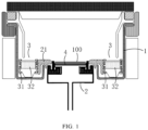
- FIG. 1 illustrates a schematic cross-section structural diagram of a process chamber according to some embodiments of the present disclosure.
- the process chamber includes chamber body 1, a base 2, and a magnetic conductive device.
- Base 2 is arranged in chamber body 1.
- Base 2 includes a carrier surface configured to carry a wafer 100.
- the magnetic conductive device includes a magnet structure 3 and a magnetic conductive structure 4 made of a soft magnetic material.
- the magnet structure 3 is arranged around base 2 and configured to provide a magnetic field above the base 2.
- the magnetic conductive structure 4 is arranged under the carrier surface of the base 2, has a preset distance from the carrier surface of the base 2, and is configured to guide the distribution of the magnetic field lines of the magnetic field above the base 2.
- the intensity of the magnetic field above base 2 is uniformly distributed, and directions of the magnetic field lines at different positions of the corresponding carrier surface are consistent.
- the magnetic conductive structure 4 is made of a soft magnetic material, the soft magnetic material does not have an excessive influence on the magnetic field compared to a hard magnetic material. Thus, the magnetic conductive structure 4 can be ensured to properly guide the magnetic field line distribution of the magnetic field above the base 2 by ensuring that the magnetic structure 3 can normally guide the magnetic field, which avoids the excessive influence on the magnetic structure 3 to cause failure in guiding the magnetic field. Meanwhile, since the soft magnetic material does not have an N pole and an S pole, the directions of the magnetic field lines generated by the soft magnetic material may not be formed in an arc shape. Thus, the soft magnetic material can guide the magnetic field lines of the magnetic field above the base 2 to be parallel with the surface of the wafer.
- the process chamber is specifically configured to perform a magnetron sputtering process or other processes, such as a physical vapor deposition or chemical deposition process.
- a magnetron sputtering process or other processes such as a physical vapor deposition or chemical deposition process.
- base 2 is arranged in the chamber body 1, for example, at a middle position near the bottom.
- the base 2 is configured to carry the wafer 100.
- the magnet structure 3 can be made of NdFeB material. However, embodiments of the present disclosure are not limited to this, as long as the magnet structure 3 is made of a hard magnetic material. Magnet structure 3 can be arranged around the base 2 and configured to provide a magnetic field above the base 2. The magnetic field can be used as an inducing magnetic field to induce an easy magnetization direction of a magnetic film.
- the magnetic conductive structure 4 can be made of a permalloy to form a sheet-shaped structure. However, embodiments of the present disclosure are not limited to this, as long as the magnetic conductive structure 4 is made of a soft magnetic material with magnetic permeability.
- the magnetic conductive structure 4 can be arranged below the carrier surface of the base 2, can have a preset distance from the carrier surface of the base 2, and can be configured to guide the magnetic field line distribution of the magnetic field above the base 2 to cause the intensity of the magnetic field to be distributed uniformly and the magnetic field lines to be consistent above the base 2.
- the above preset distance can be set according to the magnetic field line distribution of the magnetic field above the base 2, as long as the intensity of the magnetic field above the base 2 can be uniformly distributed and the directions of the magnetic field lines at different positions of the corresponding carrier surface can be consistent.
- the above magnetic conductive structure 4 can be arranged inside the base 2.
- the above magnetic conductive structure 4 can have a magnet yoke function to constrain the magnetic field lines.
- the magnetic field line distribution of the magnetic field generated by magnet structure 3 can be changed above the base.
- FIG. 10(a) when the magnetic conductive structure 4 is not arranged under wafer 100, the magnetic field lines from the N pole to the S pole of the magnet column 32 are in an arc shape.
- the magnetic field directions at different positions of the corresponding carrier surface of the base 2 in the radial direction can be normal directions of the arc at different positions.
- the directions of the magnetic field lines at different positions of the corresponding carrier surface can be different.
- the distribution of the magnetic field intensity cannot be uniform at different positions of the corresponding carrier surface of the base 2.
- the magnetic field intensity at a center area of the corresponding carrier surface of the base 2 can be smaller than the magnetic field intensity at an edge area of the corresponding carrier surface of the base 2.
- the magnetic conductive structure 4 is arranged under wafer 100.
- the magnetic conductive structure 4 can effectively guide the magnetic field line distribution of the magnetic field above the base to cause the directions of the magnetic field lines above the wafer 100 to be consistent.
- the directions of the magnetic field lines above the wafer 100 tend to be parallel to the surface of the wafer 100.
- the magnetic particles deposited at different positions of the wafer 100 can be subjected to magnetic forces in the same horizontal direction to cause the magnetic particles to generate a certain amount of lateral movement.
- the speed of the magnetic particles vertically incident to the wafer 100 can be greatly weakened to reduce the incident energy of the magnetic particles, reduce the crystal defects caused by the high-energy magnetic particles to the film, reduce the internal stress of the film, and improve the crystallization quality of the film.
- the magnetic conductive structure 4 can also make the magnetic field lines above the wafer 100 evenly distributed.
- the magnetic field intensity above the base can be evenly distributed, which causes hard and easy axes of the film to be consistent at the positions of the wafer to significantly improve the magnetic anisotropy of the film.
- the magnetic conductive structure is arranged under the carrier surface of the base.
- the magnetic conductive structure can be configured to guide the distribution of the magnetic field lines of the magnetic field generated by the magnet structure above the base. That is, the magnetic conductive structure can have a magnetic yoke function to constrain the magnetic field lines.
- the intensity of the magnetic field above the base can be uniformly distributed, and the directions of the magnetic field lines can be consistent at different positions of the corresponding carrier surface. Therefore, the hard and easy axes can be consistent at the positions of the wafer to significantly improve the magnetic anisotropy of the film.
- the incident energy of the magnetic particles can be reduced, the crystal defects caused by the high-energy magnetic particles in the film can be reduced, the internal stress of the film can be reduced, and the crystallization quality of the film can be improved.
- the above magnetic conductive structure can significantly improve the magnetic anisotropy of the film, a buffer layer and an annealing process of the existing technology may not need to be used to improve the magnetic anisotropy of the film.
- the crystal defects of the film can be effectively reduced, and the film quality can be improved.
- the above magnetic conductive structure 4 includes a magnetic conductive assembly.
- the magnetic conductive assembly includes a plurality of first magnetic conductive bars 43.
- the plurality of first magnetic conductive bars 43 can be evenly distributed in a circular area parallel to and opposite to the carrier surface of the base 2.
- the circular area for example, can be arranged concentrically with the carrier surface.
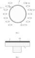
- the plurality of first magnetic conductive bars 43 can be extended and arranged along a first direction parallel to the carrier surface (i.e., direction X in FIG. 2 ). For example, as shown in FIG. 2 , lengths of the plurality of first magnetic conductive bars 43 in direction X are different from each other.
- An orthographic projection contour of the plurality of first magnetic conductive bars 43 on the carrier surface can be circular to ensure that the plurality of first magnetic conductive bars 43 are evenly distributed in the above circular area.
- the intensity of the magnetic field above the base can be evenly distributed and the directions of the magnetic field lines can be consistent at different positions of the corresponding carrier surface.
- a distance between any two adjacent first magnetic conductive bars 43 can be greater than or equal to 4 mm and less than or equal to 8 mm, for example, 4 mm, 5 mm, 6 mm, 7 mm, or 8 mm.
- the magnetic field lines can be ensured to be sufficiently restrained, and meanwhile, the intensity of the magnetic field above the base can be evenly distributed, and the directions of the magnetic field lines can be consistent at different positions of the corresponding carrier surface.
- embodiments of the present disclosure are not limited to this, and those skilled in the art can adjust the settings by themselves according to different process requirements.
- the magnetic conductive structure 4 further includes a fixing ring 42.
- An inner side of the fixing ring 42 can be configured to define the above circular area.
- the fixing ring 42 can be connected to the above magnetic conductive assembly and configured to fix the magnetic conductive assembly in base 2.
- the plurality of first magnetic conductive bars 43 are arranged on the inner side of the fixing ring 42. Two ends of each first magnetic conductive bar 43 can be fixedly connected to the fixing ring 42.
- the fixed connection can include, for example, an adhesive connection, a bolt connection, or welding.
- the fixing ring 42 can be arranged in base 2 in a detachable manner such as a bolt connection to facilitate assembly and replacement of the fixing ring 42.
- the above fixing ring 42 may not be arranged, and the magnetic conductive assembly can be fixed in the base 2 in any other manner.
- the fixing ring 42 can also be made of a soft magnetic material.
- the fixing ring 42 and the first magnetic conductive bars 43 can be made of the same soft magnetic material to achieve a better magnetic conductive effect.
- a diameter of the circular area can be smaller than a diameter of the carrier surface of the base 2.
- a ratio of the diameter of the circular area to the diameter of the carrier surface of the base 2 can be greater than or equal to two-thirds and less than or equal to one.
- the diameter of the outer ring of the fixing ring 42 can be smaller than or equal to the diameter of the carrier surface of the base 2.
- the thickness of the magnetic conductive structure 4 can be greater than or equal to 2 mm and less than or equal to 10 mm.
- the preset distance can be greater than or equal to 2 mm and less than or equal to 5 mm.
- embodiments of the present disclosure are not limited to this. Those skilled in the art can adjust the settings by themselves according to different process requirements.
- the magnet structure 3 includes two groups of magnet groups and a fixing bracket 31.
- the fixing bracket 31 can be configured to fix the two groups of magnet groups around base 2.
- the two groups of magnet groups are arranged oppositely on two sides of base 2 (for example, left and right sides in FIG. 2 ) along the radial direction of the carrier surface of the base 2.
- Each group of magnet group can include a plurality of magnet columns 32.
- the plurality of magnet columns 32 can be arranged in an arc shape along a circumferential direction of the above carrier surface.
- N poles and the S poles of all the magnet columns 32 in the two groups of magnet groups are arranged at a same height along a second direction (i.e., direction Y in FIG. 2 ).
- the second direction can be parallel to the radial direction of the base 2 and form a preset angle with the first direction (i.e., direction X in FIG. 2 ).
- the preset angle in FIG. 2 is 90°.
- the above preset angle can be greater than or equal to 0° and less than or equal to 90°, for example, 0°, 10°, 30°, 50°, 60 °, or 80°.
- the N poles of all the magnet columns 32 in one group of magnet groups i.e., the magnet group on the left side in FIG. 2
- S poles of all the magnet columns 32 in the other group of magnet groups i.e., the magnet group on the right side in FIG. 2
- embodiments of the present disclosure can be meet different process requirements to greatly improve the applicability and scope of application. Moreover, with the above design of the magnetic conductive structure 4, embodiments of the present disclosure can have a simple structure and be easy to be implemented, and the application and maintenance costs can be effectively reduced and maintained.
- the space on the upper surface of the base 2 can be greatly saved, which causes embodiments of the present disclosure to be suitable for a large size wafer, for example, a 12-inch wafer.
- the magnet columns 32 have a certain distance from the base 2, which avoids the problem that the magnetic property of the magnet column is degraded due to the temperature change of the base in the existing technology.
- the service life of the magnet structure 3 can be greatly increased, and the distribution of the magnet columns 32 can also be helpful to improve the uniformity of the film.
- the purpose of adjusting the intensity of the magnetic field and the magnetic field distribution can be achieved near the wafer.
- the magnetic anisotropy of the film can be adjusted.
- an upper end of the magnet column 32 can be flush with the upper surface of the wafer 100 arranged on the carrier surface.
- the magnetic field lines can be ensured to be distributed near the top of the wafer 100.
- the magnet column 32 can be a cylinder, a cuboid, etc.
- the fixing bracket 31 can be made of a metal material or a non-metal material, as long as the fixing bracket 31 is corrosion-resistant and does not affect the magnetic property of the magnet column 32.
- the fixing bracket 31 can be arranged between a side wall of the chamber body 1 and a cover ring 21 of the base 2.
- two fixing brackets 31 can be provided.
- the two fixing brackets 31 can be arranged on two opposite sides of base 2 and configured to fix the two groups of magnet groups, respectively.
- embodiments of the present disclosure are not limited to this.
- embodiments of the present disclosure do not necessarily include the fixing bracket 31.
- the magnet columns 32 can also be arranged in chamber body 1 in another manner.
- the magnet columns 32 can be directly bonded to the bottom wall of chamber body 1.
- Embodiments of the present disclosure are not limited to this, and those skilled in the art can adjust the settings by themselves according to the actual situation.
- embodiments of the present disclosure do not limit the magnetic conductive structure 4 to have a split structure.
- the magnetic conductive structure 4 can also be formed integrally.
- Embodiments of the present disclosure are not limited to this, and those skilled in the art can adjust the settings according to the actual situation.
- the magnetic conductive structure 4 can include a plurality of through-holes (not shown in the figure) corresponding to support thimbles of the base 2.
- the inner diameters of the through-holes can be larger than the outer diameters of the support thimbles for the thimbles to pass through, which avoids mechanical interference of the base 2 during ascending and descending processes of the support thimbles and transferring the wafer to effectively reduce a failure rate of embodiments of the present disclosure.
- the magnetic conductive assembly further includes a plurality of second magnetic conductive bars 44 and a plurality of magnetic conductive rings 45.
- the plurality of second magnetic conductive bars 44 are distributed in a circular area parallel to and opposite to the carrier surface of the base 2 and extend along different radial directions of the circular area.
- the plurality of second magnetic conductive bars 44 can be symmetrically arranged to the center of the above circular area.
- the plurality of magnetic conductive rings 45 can be arranged in the above circular area and overlap with the plurality of second magnetic conductive bars 44. Centers of the plurality of magnetic conductive rings 45 can coincide with the center of the above circular area.
- the plurality of magnetic conductive rings 45 can have different inner diameters and be arranged along the radial direction of the above circular area at an equal interval.
- FIG. 3 shows four second magnetic conductive bars 44.
- the four second magnetic conductive bars 44 can extend along different radial directions of the circular area to form a structure similar to a "*" shape.
- the distribution of the magnetic field lines can be guided above base 2.
- the intensity of the magnetic field can be evenly distributed above the base 2, and the directions of the magnetic field lines can be consistent. Since the design of the structure is simple and appropriate, the application cost and the maintenance cost can be greatly reduced.
- fixing ring 42 can be also provided.
- the structure and function of the fixing ring 42 can be the same as the structure and function of the fixing ring 42 in FIG. 2 , which is not repeated here.
- the magnetic conductive assembly further includes a magnetic conductive plate 46.
- the magnetic conductive plate 46 can be arranged parallel to and opposite to the carrier surface of the base 2, which can also guide the distribution of the magnetic field lines of the magnetic field above the base 2.
- the intensity of the magnetic field can be uniformly distributed above the base 2, and the directions of the magnetic field lines can be consistent.
- a fixing ring 42 can be also provided.
- the structure and function of the fixing ring 42 can be the same as the structure and function of the fixing ring 42 in FIG. 2 , which is not repeated here.
- an outer surface of each magnet column 32 can be covered with an anti-corrosion layer made of a soft magnetic material (not shown in the figure).
- the anti-corrosion layer can be specifically made of soft magnetic material, such as stainless steel, silicon steel, or low-carbon steel.
- the anti-corrosion layer can be used to greatly increase the strength of the magnet column 32 without affecting the magnetic property of the magnet column 32 to facilitate the assembly and maintenance of the magnet column 32.
- the anti-corrosion layer can be used to prevent the magnet column 32 from being corroded to greatly improve the service life of the magnet column 32.
- FIG. 6 and FIG. 7 show specific simulation results.
- FIG. 6 shows a simulation result of the existing technology.
- FIG. 7 shows a simulation result of embodiments of the present disclosure.
- FIG. 6 and FIG. 7 show the distributions of the magnetic fields at a distance of 2 mm above the upper surface of the wafer.
- the direction of the magnetic field of the area can be the direction indicated by the small arrow.
- Same areas are selected from FIG. 6 and FIG. 7 , that is, areas within ellipse dotted lines in FIG. 6 and FIG. 7 .
- the intensity of the magnetic field is more evenly distributed near the top of the wafer in embodiments of the present disclosure, and the directions of the magnetic field lines are more consistent.
- FIG. 8 and FIG. 9 show schematic diagrams showing changes in intensity components of the magnetic fields in the existing technology and embodiments of the present disclosure, respectively.
- the intensity components of the magnetic fields at a distance of 2 mm above the upper surface of the wafer in direction x and direction y of FIG. 6 and FIG. 7 are component Bx and component By, respectively.
- the ordinate represents the intensity of the magnetic field, and the abscissa represents the distance.
- FIG. 8 and FIG. 9 show schematic diagrams showing changes in intensity components of the magnetic fields in the existing technology and embodiments of the present disclosure, respectively.
- the intensity components of the magnetic fields at a distance of 2 mm above the upper surface of the wafer in direction x and direction y of FIG. 6 and FIG. 7 are component Bx and component By, respectively.
- component Bx and component By are substantially the same at the edge and the center at a distance of 2 mm from the upper surface of the wafer. Thus, the uniformity of the magnetic field distribution can be good.
- embodiments of the present disclosure provide a semiconductor process apparatus, including the process chamber of the semiconductor process apparatus of the above embodiments.
- the magnetic conductive structure can be arranged under the carrier surface of the base.
- the magnetic conductive structure can be configured to guide the distribution of the magnetic field lines of the magnetic field generated by the magnet structure above the base. That is, the magnetic conductive structure can have a magnetic yoke function to constrain the magnetic field lines.
- the intensity of the magnetic field above the base can be uniformly distributed, and the directions of the magnetic field lines at different positions of the corresponding carrier surface can be consistent.
- the hard and easy axes of the film at the positions of the wafer can be consistent to significantly improve the magnetic anisotropy of the film.
- the incident energy of the magnetic particles can be reduced, and the crystal defects caused by the high-energy magnetic particles in the film can be reduced.
- the internal stress of the film can be reduced, and the crystallization quality of the film can be improved.
- the buffer layer and the annealing process of the existing technology may not be needed to improve the magnetic anisotropy of the film, which can effectively reduce the crystal defects of the film to improve the film quality.
- first and second are only used for description, and should not be construed as indicating or implying relative importance or implicitly indicating the number of technical features indicated. Thus, a feature defined as “first” or “second” may expressly or implicitly include one or more of the features. In the description of the present disclosure, unless otherwise specified, "a plurality of' means two or more.
- the terms “installed,” “connected,” and “coupled” should be understood in a broad sense.
- the terms can mean a fixed connection or a detachable connection, an integral connection, a direct connection, an indirect connection through an intermediate medium, or internal communication of two elements.
- the specific meanings of the above terms in the present disclosure can be understood according to specific situations.
Landscapes
- Chemical & Material Sciences (AREA)
- Engineering & Computer Science (AREA)
- Chemical Kinetics & Catalysis (AREA)
- Materials Engineering (AREA)
- Mechanical Engineering (AREA)
- Metallurgy (AREA)
- Organic Chemistry (AREA)
- Physics & Mathematics (AREA)
- Plasma & Fusion (AREA)
- Analytical Chemistry (AREA)
- Power Engineering (AREA)
- Thermal Sciences (AREA)
- Manufacturing & Machinery (AREA)
- Electromagnetism (AREA)
- Physical Vapour Deposition (AREA)
- Thin Magnetic Films (AREA)
- Hall/Mr Elements (AREA)
- Container, Conveyance, Adherence, Positioning, Of Wafer (AREA)
- Crystals, And After-Treatments Of Crystals (AREA)
Abstract
Description
- The present disclosure generally relates to the semiconductor manufacturing technology field and, more particularly, to a semiconductor process apparatus and a process chamber.
- Currently, an integrated circuit is a miniature electronic device or component. Transistors, resistors, capacitors, inductors, and other components and wiring required in a circuit are interconnected using a certain process. The integrated circuit is fabricated on one or several small semiconductor wafers or dielectric substrates and then packaged in a tube case to form a microstructure with a required circuit function. With the development of electronic devices in a direction of miniaturization, high frequency, integration, and functionalization, an electromagnetic compatibility problem of the components such as transistors, resistors, capacitors, and inductors interconnected by wiring becomes more and more serious. In a process of integrating electronic devices using a high-frequency microwave, an electromagnetic environment becomes more and more complex, and electromagnetic compatibility requirements of elements become higher and higher. Anti-electromagnetic interference has become a problem attracting attention.
- Anti-electromagnetic interference electronic devices made of a special material in the existing technology has become an important direction for developing electromagnetic compatibility in the future. For example, by applying the high-frequency magnetic film on a side of the electronic devices and microwave circuits, a high-frequency noise signal can be effectively absorbed and inhibited. After continuous exploration and experiments, when a magnet is magnetized, an easy magnetization direction and a hard magnetization direction exist, because the magnet is magnetic anisotropy (i.e., all or some chemical or physical properties of a substance change as a direction changes and are different in different directions). In the easy magnetization direction, the anisotropy of a magnet crystal is small. In the hard magnetization direction, the anisotropy of the magnet crystal is large. The direction of the anisotropy field can affect the induction of the film to the electromagnetic field to affect the absorption effect of the film for the noise. Thus, it is important to fabricate high-frequency magnetic film with high magnetic anisotropy on a large scale.
- In existing technology, magnetron sputtering technology is mainly used to fabricate the high-frequency magnetic film. During the preparation process, the wafer is arranged in a middle position of the magnetic group configured to generate an induced magnetic field. The magnetic group can form the induced magnetic field in a direction parallel to the film surface of the substrate to induce the easy magnetization direction of the magnetic film, and meanwhile, a buffer layer or different buffer layers are deposited on the substrate to increase the magnetic anisotropy. Then, an annealing process is performed on the magnetic film to maintain the magnetic anisotropy of the magnetic film well. For example, when NiFeCr/NiFe/Ta films are fabricated, the induced magnetic field generated by the magnet group is used to induce the easy magnetization direction of the nickel-iron (NiFe) film, and a tantalum (Ta) buffer layer and a nickel-iron-chromium (NiFeCr) buffer layer are deposited on the substrate. Then, the annealing processing is performed on the Ni81Fe19/tantalum (Ta) film with tantalum (Ta) buffer layer and the Ni81Fe19/tantalum (Ta) film with nickel-iron-chromium (NiFeCr) buffer layer. After the annealing processing at 350 °C, the magnetic anisotropy of Ni81Fe19 films can be well maintained.
- However, the intensity of the above-induced magnetic field is not sufficiently evenly distributed above the wafer, which causes the film deposited on the wafer to have poor magnetic anisotropy. Moreover, since the magnetic field lines of the induced magnetic field are in the arc shape above the wafer, the incident magnetic particles to the wafer have high speed and energy. Thus, crystal defects are generated in the film, the internal stress of the film is increased, and the crystallization quality of the film is poor.
- For the existing disadvantage, the present disclosure provides a semiconductor process apparatus and a process chamber configured to solve the technical problem that the quality and the magnetic anisotropy of the film are poor in the existing technology.
- On one aspect, the present disclosure provides a process chamber of a semiconductor process apparatus, including a chamber body, a base, and a magnetic conductive device.
- The base is arranged in the chamber body, and the base includes a carrier surface configured to carry a wafer.
- The magnetic conductive device includes a magnet structure and a magnetic conductive structure made of a soft magnetic material. The magnet structure is arranged around the base and configured to provide a magnetic field above the base. The magnetic conductive structure is arranged under the carrier surface of the base, has a preset distance from the carrier surface of the base, and is configured to guide distribution of magnetic field lines of the magnetic field above the base to cause intensity of the magnetic field to be evenly distributed above the base and directions of the magnetic field lines to be consistent at different positions of the carrier surface.
- In some embodiments, the magnetic conductive structure includes a magnetic conductive assembly. The magnetic conductive assembly includes a plurality of first magnetic conductive bars. The plurality of first magnetic conductive bars are distributed evenly in a circular area that is parallel to and opposite to the carrier surface. The plurality of first magnetic conductive bars extend along a first direction parallel to the carrier surface.
- In some other embodiments, the magnetic conductive assembly includes a plurality of second magnetic conductive bars and a plurality of magnetic conductive rings. The plurality of second magnetic conductive bars are distributed in the circular area and extend different radial directions of the circular area. The plurality of second magnetic conductive bars is symmetrically distributed about the center of the circular area. The plurality of magnetic conductive rings are arranged in the circular area and overlap with the plurality of second magnetic conductive bars. The centers of the plurality of magnetic conductive rings coincide with the center of the circular area. Inner diameters of the plurality of magnetic conductive rings are different. The plurality of magnetic conductive rings are arranged at the same interval along a radial direction of the circular area.
- In some other embodiments, the magnetic conductive assembly includes a magnetic conductive plate. The magnetic conductive plate is arranged parallel to and oppositely to the carrier surface.
- In some embodiments, a distance between any two neighboring first magnetic conductive bars of the first magnetic conductive bars is greater than or equal to 4 mm and smaller than or equal to 8 mm.
- In some embodiments, a ratio of a diameter of the circular area to a diameter of the carrier surface is greater than or equal to two thirds and smaller than or equal to one.
- In some embodiments, the magnetic conductive structure further includes a fixing ring, an inner side of the fixing ring forms the circular area, and the fixing ring is connected to the magnetic conductive assembly and configured to fix the magnetic conductive assembly in the base.
- In some embodiments, the magnet structure includes two groups of magnet groups and a fixing bracket. The fixing bracket is configured to fix the two groups of magnet groups around the base.
- The two groups of magnet groups are arranged on two sides of the base along a radial direction of the carrier surface. Each group of magnet groups includes a plurality of magnet columns. The plurality of magnet columns are arranged in an arc shape along the circumference of the carrier surface at intervals. N poles and S poles of all magnet columns of the two groups of magnet groups are arranged along a second direction at a same height. The second direction is parallel to the radial direction of the base and has a preset angle with the first direction. N poles of magnet columns of one group of magnet groups are close to the base. S poles of magnet columns of the other group of magnet groups are close to the base.
- In some embodiments, the preset angle is 90°.
- In some embodiments, the outer surface of a magnet column is covered with an anti-corrosion layer made of a soft magnetic material.
- In some embodiments, a thickness of the magnetic conductive structure is greater than or equal to 2 mm and smaller than or equal to 10 mm, and the preset distance is greater than or equal to 2 mm and smaller than or equal to 5 mm.
- On a second aspect, embodiments of the present disclosure provide a semiconductor process apparatus, including the process chamber of the semiconductor process apparatus of the first aspect.
- The beneficial technical effects brought by the technical solutions of embodiments of the present disclosure are as follows.
- In embodiments of the present disclosure, the magnetic conductive structure is arranged under the carrier surface of the base. The magnetic conductive structure is configured to guide the distribution of the magnetic field lines of the magnetic field generated by the magnet structure above the base. That is, the magnetic conductive structure can have the magnetic yoke function to constrain the magnetic field lines. Thus, the intensity of the magnetic field can be evenly distributed above the base, and the directions of the magnetic field lines can be consistent at different positions of the corresponding carrier surface. Thus, hard and easy axes of the film can be consistent at different positions of the wafer to significantly improve the magnetic anisotropy of the film, reduce the incident energy of the magnetic particles, reduce the crystal defects of the film caused by the high-energy magnetic particles, and reduce the internal stress of the film. Thus, the crystallization quality of the film is improved. In addition, since the above magnetic conductive structure can significantly improve the magnetic anisotropy of the film, the buffer layer and the annealing process of the existing technology are not needed to improve the magnetic anisotropy of the film. Thus, the crystal defects of the film can be effectively reduced to improve the quality of the film.
- Additional aspects and advantages of the present disclosure are partially described and become apparent through the following description or through the implementation of the present disclosure.
- The above and/or additional aspects and advantages of the present disclosure become apparent and easy to understand from the following description of embodiments in connection with the accompanying drawings.
-
FIG. 1 illustrates a schematic cross-section structural diagram of a process chamber according to some embodiments of the present disclosure. -
FIG. 2 illustrates a schematic top view of a magnetic conductive structure and a magnet structure according to some embodiments of the present disclosure. -
FIG. 3 illustrates a schematic top view of another magnetic conductive structure and another magnet structure according to some embodiments of the present disclosure. -
FIG. 4 illustrates a schematic top view of another magnetic conductive structure and another magnet structure according to some embodiments of the present disclosure. -
FIG. 5 illustrates a schematic cross-section structural diagram of a base according to some embodiments of the present disclosure. -
FIG. 6 illustrates a schematic diagram showing a simulation result of a magnetic field distribution in a process chamber in the existing technology. -
FIG. 7 illustrates a schematic diagram showing a simulation result of a magnetic field distribution in a process chamber according to some embodiments of the present disclosure. -
FIG. 8 illustrates a schematic diagram showing a change in a magnetic intensity component in the process chamber in the existing technology. -
FIG. 9 illustrates a schematic diagram showing a change in a magnetic intensity component in the process chamber according to some embodiments of the present disclosure. -
FIG. 10 illustrates a schematic diagram showing magnetic field line distributions of a magnetic field above a wafer when a magnetic conductive structure is not arranged under the wafer and the magnetic conductive structure is arranged under the wafer according to embodiments of the present disclosure. - The present disclosure is described in detail below. Examples of embodiments of the present disclosure are illustrated in the accompanying drawings. The same or similar reference numerals refer to the same or similar members or members having the same or similar functions throughout. In addition, a detailed description of known technology is omitted if the detailed description of the known technology is not necessary for illustrating features of the present disclosure. Embodiments described below with reference to the accompanying drawings are exemplary and are only used to explain the present disclosure, but are not to be considered to limit the present disclosure.
- Those skilled in the art can understand that, unless otherwise defined, all terms (including technical and scientific terms) used here have the same meaning as commonly understood by those of ordinary skill in the art to which the present disclosure belongs. It should also be understood that terms, such as those defined in a general dictionary, should be understood to have meanings consistent with meanings in the context of the existing technology. Unless specifically defined here, the terms should not be interpreted with idealistic or overly formal meanings.
- The technical solutions of the present disclosure and how the above technical problems are solved in the technical solutions of the present disclosure are described in detail below with specific embodiments.
-
FIG. 1 illustrates a schematic cross-section structural diagram of a process chamber according to some embodiments of the present disclosure. As shown inFIG. 1 , embodiments of the present disclosure provide the process chamber of a semiconductor process apparatus. The process chamber includeschamber body 1, abase 2, and a magnetic conductive device.Base 2 is arranged inchamber body 1.Base 2 includes a carrier surface configured to carry awafer 100. The magnetic conductive device includes amagnet structure 3 and a magneticconductive structure 4 made of a soft magnetic material. Themagnet structure 3 is arranged aroundbase 2 and configured to provide a magnetic field above thebase 2. The magneticconductive structure 4 is arranged under the carrier surface of thebase 2, has a preset distance from the carrier surface of thebase 2, and is configured to guide the distribution of the magnetic field lines of the magnetic field above thebase 2. Thus, the intensity of the magnetic field abovebase 2 is uniformly distributed, and directions of the magnetic field lines at different positions of the corresponding carrier surface are consistent. - Since the magnetic
conductive structure 4 is made of a soft magnetic material, the soft magnetic material does not have an excessive influence on the magnetic field compared to a hard magnetic material. Thus, the magneticconductive structure 4 can be ensured to properly guide the magnetic field line distribution of the magnetic field above thebase 2 by ensuring that themagnetic structure 3 can normally guide the magnetic field, which avoids the excessive influence on themagnetic structure 3 to cause failure in guiding the magnetic field. Meanwhile, since the soft magnetic material does not have an N pole and an S pole, the directions of the magnetic field lines generated by the soft magnetic material may not be formed in an arc shape. Thus, the soft magnetic material can guide the magnetic field lines of the magnetic field above thebase 2 to be parallel with the surface of the wafer. - As shown in
FIG. 1 , the process chamber is specifically configured to perform a magnetron sputtering process or other processes, such as a physical vapor deposition or chemical deposition process. However, embodiments of the present disclosure are not limited to this. Specifically,base 2 is arranged in thechamber body 1, for example, at a middle position near the bottom. Thebase 2 is configured to carry thewafer 100. - In the magnetic conductive device, the
magnet structure 3 can be made of NdFeB material. However, embodiments of the present disclosure are not limited to this, as long as themagnet structure 3 is made of a hard magnetic material.Magnet structure 3 can be arranged around thebase 2 and configured to provide a magnetic field above thebase 2. The magnetic field can be used as an inducing magnetic field to induce an easy magnetization direction of a magnetic film. - The magnetic
conductive structure 4 can be made of a permalloy to form a sheet-shaped structure. However, embodiments of the present disclosure are not limited to this, as long as the magneticconductive structure 4 is made of a soft magnetic material with magnetic permeability. The magneticconductive structure 4 can be arranged below the carrier surface of thebase 2, can have a preset distance from the carrier surface of thebase 2, and can be configured to guide the magnetic field line distribution of the magnetic field above thebase 2 to cause the intensity of the magnetic field to be distributed uniformly and the magnetic field lines to be consistent above thebase 2. The above preset distance can be set according to the magnetic field line distribution of the magnetic field above thebase 2, as long as the intensity of the magnetic field above thebase 2 can be uniformly distributed and the directions of the magnetic field lines at different positions of the corresponding carrier surface can be consistent. - In some optional embodiments, to facilitate the installation and fixation of the magnetic
conductive structure 4, the above magneticconductive structure 4 can be arranged inside thebase 2. - The above magnetic
conductive structure 4 can have a magnet yoke function to constrain the magnetic field lines. Thus, the magnetic field line distribution of the magnetic field generated bymagnet structure 3 can be changed above the base. As shown inFIG. 10(a) , when the magneticconductive structure 4 is not arranged underwafer 100, the magnetic field lines from the N pole to the S pole of themagnet column 32 are in an arc shape. The magnetic field directions at different positions of the corresponding carrier surface of thebase 2 in the radial direction can be normal directions of the arc at different positions. Thus, the directions of the magnetic field lines at different positions of the corresponding carrier surface can be different. Moreover, the distribution of the magnetic field intensity cannot be uniform at different positions of the corresponding carrier surface of thebase 2. Specifically, the magnetic field intensity at a center area of the corresponding carrier surface of thebase 2 can be smaller than the magnetic field intensity at an edge area of the corresponding carrier surface of thebase 2. - In a process of depositing magnetic particles on the surface of
wafer 100, due to the uneven distribution of the magnetic field intensity above thewafer 100, magnetic anisotropy of a film deposited on thewafer 100 can be poor. Moreover, since the directions of the magnetic field lines at different positions of the corresponding carrier surface are different, a speed and energy of a magnetic particle incident to thewafer 100 can be relatively high, which causes a crystal defect in the film to increase internal stress of the film. Thus, crystallization quality of the film can be poor. - As shown in
FIG. 10(b) , the magneticconductive structure 4 is arranged underwafer 100. The magneticconductive structure 4 can effectively guide the magnetic field line distribution of the magnetic field above the base to cause the directions of the magnetic field lines above thewafer 100 to be consistent. As shown inFIG. 10(b) , the directions of the magnetic field lines above thewafer 100 tend to be parallel to the surface of thewafer 100. Thus, the magnetic particles deposited at different positions of thewafer 100 can be subjected to magnetic forces in the same horizontal direction to cause the magnetic particles to generate a certain amount of lateral movement. Thus, the speed of the magnetic particles vertically incident to thewafer 100 can be greatly weakened to reduce the incident energy of the magnetic particles, reduce the crystal defects caused by the high-energy magnetic particles to the film, reduce the internal stress of the film, and improve the crystallization quality of the film. Meanwhile, the magneticconductive structure 4 can also make the magnetic field lines above thewafer 100 evenly distributed. Thus, the magnetic field intensity above the base can be evenly distributed, which causes hard and easy axes of the film to be consistent at the positions of the wafer to significantly improve the magnetic anisotropy of the film. - In embodiments of the present disclosure, the magnetic conductive structure is arranged under the carrier surface of the base. The magnetic conductive structure can be configured to guide the distribution of the magnetic field lines of the magnetic field generated by the magnet structure above the base. That is, the magnetic conductive structure can have a magnetic yoke function to constrain the magnetic field lines. Thus, the intensity of the magnetic field above the base can be uniformly distributed, and the directions of the magnetic field lines can be consistent at different positions of the corresponding carrier surface. Therefore, the hard and easy axes can be consistent at the positions of the wafer to significantly improve the magnetic anisotropy of the film. In addition, the incident energy of the magnetic particles can be reduced, the crystal defects caused by the high-energy magnetic particles in the film can be reduced, the internal stress of the film can be reduced, and the crystallization quality of the film can be improved. In addition, since the above magnetic conductive structure can significantly improve the magnetic anisotropy of the film, a buffer layer and an annealing process of the existing technology may not need to be used to improve the magnetic anisotropy of the film. Thus, the crystal defects of the film can be effectively reduced, and the film quality can be improved.
- In an embodiment of the present disclosure, as shown in
FIG. 2 , the above magneticconductive structure 4 includes a magnetic conductive assembly. The magnetic conductive assembly includes a plurality of first magnetic conductive bars 43. The plurality of first magneticconductive bars 43 can be evenly distributed in a circular area parallel to and opposite to the carrier surface of thebase 2. The circular area, for example, can be arranged concentrically with the carrier surface. The plurality of first magneticconductive bars 43 can be extended and arranged along a first direction parallel to the carrier surface (i.e., direction X inFIG. 2 ). For example, as shown inFIG. 2 , lengths of the plurality of first magneticconductive bars 43 in direction X are different from each other. An orthographic projection contour of the plurality of first magneticconductive bars 43 on the carrier surface can be circular to ensure that the plurality of first magneticconductive bars 43 are evenly distributed in the above circular area. Thus, the intensity of the magnetic field above the base can be evenly distributed and the directions of the magnetic field lines can be consistent at different positions of the corresponding carrier surface. In some embodiments, a distance between any two adjacent first magneticconductive bars 43 can be greater than or equal to 4 mm and less than or equal to 8 mm, for example, 4 mm, 5 mm, 6 mm, 7 mm, or 8 mm. By setting the distance within this range, the magnetic field lines can be ensured to be sufficiently restrained, and meanwhile, the intensity of the magnetic field above the base can be evenly distributed, and the directions of the magnetic field lines can be consistent at different positions of the corresponding carrier surface. Of course, embodiments of the present disclosure are not limited to this, and those skilled in the art can adjust the settings by themselves according to different process requirements. - In an embodiment of the present disclosure, as shown in
FIG. 2 , the magneticconductive structure 4 further includes a fixingring 42. An inner side of the fixingring 42 can be configured to define the above circular area. The fixingring 42 can be connected to the above magnetic conductive assembly and configured to fix the magnetic conductive assembly inbase 2. Specifically, the plurality of first magneticconductive bars 43 are arranged on the inner side of the fixingring 42. Two ends of each first magneticconductive bar 43 can be fixedly connected to the fixingring 42. The fixed connection can include, for example, an adhesive connection, a bolt connection, or welding. In addition, the fixingring 42 can be arranged inbase 2 in a detachable manner such as a bolt connection to facilitate assembly and replacement of the fixingring 42. Of course, in practical applications, theabove fixing ring 42 may not be arranged, and the magnetic conductive assembly can be fixed in thebase 2 in any other manner. - In an embodiment of the present disclosure, the fixing
ring 42 can also be made of a soft magnetic material. For example, the fixingring 42 and the first magneticconductive bars 43 can be made of the same soft magnetic material to achieve a better magnetic conductive effect. - In an embodiment of the present disclosure, a diameter of the circular area can be smaller than a diameter of the carrier surface of the
base 2. For example, a ratio of the diameter of the circular area to the diameter of the carrier surface of thebase 2 can be greater than or equal to two-thirds and less than or equal to one. By setting the diameter of the circular area within this range, the overall dimension of the magneticconductive structure 4 can be optimized by ensuring that the intensity of the magnetic field is evenly distributed above the base, and the directions of the magnetic field lines are consistent at different positions of the corresponding carrier surface. Thus, the installation of the magneticconductive structure 4 can be facilitated. Of course, in practical application, according to specific needs, for example, as shown inFIG. 5 , the diameter of the circular area is the same as the diameter of the carrier surface ofbase 2. - It should be noted that, if the fixing
ring 42 is also made of soft magnetic material, the diameter of the outer ring of the fixingring 42 can be smaller than or equal to the diameter of the carrier surface of thebase 2. - In an embodiment of the present disclosure, the thickness of the magnetic
conductive structure 4 can be greater than or equal to 2 mm and less than or equal to 10 mm. The preset distance can be greater than or equal to 2 mm and less than or equal to 5 mm. However, embodiments of the present disclosure are not limited to this. Those skilled in the art can adjust the settings by themselves according to different process requirements. - In an embodiment of the present disclosure, as shown in
FIG. 1 andFIG. 2 , themagnet structure 3 includes two groups of magnet groups and a fixingbracket 31. The fixingbracket 31 can be configured to fix the two groups of magnet groups aroundbase 2. As shown inFIG. 2 , The two groups of magnet groups are arranged oppositely on two sides of base 2 (for example, left and right sides inFIG. 2 ) along the radial direction of the carrier surface of thebase 2. Each group of magnet group can include a plurality ofmagnet columns 32. The plurality ofmagnet columns 32 can be arranged in an arc shape along a circumferential direction of the above carrier surface. N poles and the S poles of all themagnet columns 32 in the two groups of magnet groups are arranged at a same height along a second direction (i.e., direction Y inFIG. 2 ). The second direction can be parallel to the radial direction of thebase 2 and form a preset angle with the first direction (i.e., direction X inFIG. 2 ). The preset angle inFIG. 2 is 90°. Of course, in practical applications, the above preset angle can be greater than or equal to 0° and less than or equal to 90°, for example, 0°, 10°, 30°, 50°, 60 °, or 80°. Moreover, the N poles of all themagnet columns 32 in one group of magnet groups (i.e., the magnet group on the left side inFIG. 2 ) can be close to thebase 2, and S poles of all themagnet columns 32 in the other group of magnet groups (i.e., the magnet group on the right side inFIG. 2 ) can be close to thebase 2. - By extending and arranging the plurality of first magnetic
conductive bars 43 along the first direction parallel to the above carrier surface (i.e., direction X inFIG. 2 ) and having a preset angle with the second direction, embodiments of the present disclosure can be meet different process requirements to greatly improve the applicability and scope of application. Moreover, with the above design of the magneticconductive structure 4, embodiments of the present disclosure can have a simple structure and be easy to be implemented, and the application and maintenance costs can be effectively reduced and maintained. - By fixing the two groups of magnetic groups in the
chamber body 1 through the fixingbracket 31 and arranging the two groups of magnetic groups around thebase 2, on one hand, the space on the upper surface of thebase 2 can be greatly saved, which causes embodiments of the present disclosure to be suitable for a large size wafer, for example, a 12-inch wafer. On another hand, since themagnet columns 32 have a certain distance from thebase 2, which avoids the problem that the magnetic property of the magnet column is degraded due to the temperature change of the base in the existing technology. Thus, the service life of themagnet structure 3 can be greatly increased, and the distribution of themagnet columns 32 can also be helpful to improve the uniformity of the film. - In some other embodiments of the present disclosure, by changing the density of the distribution of the
magnet columns 32, the purpose of adjusting the intensity of the magnetic field and the magnetic field distribution can be achieved near the wafer. Thus, the magnetic anisotropy of the film can be adjusted. - In an embodiment of the present disclosure, an upper end of the
magnet column 32 can be flush with the upper surface of thewafer 100 arranged on the carrier surface. Thus, the magnetic field lines can be ensured to be distributed near the top of thewafer 100. - In an embodiment of the present disclosure, the
magnet column 32 can be a cylinder, a cuboid, etc. - In an embodiment of the present disclosure, the fixing
bracket 31 can be made of a metal material or a non-metal material, as long as the fixingbracket 31 is corrosion-resistant and does not affect the magnetic property of themagnet column 32. Specifically, the fixingbracket 31 can be arranged between a side wall of thechamber body 1 and acover ring 21 of thebase 2. - In an embodiment of the present disclosure, two fixing
brackets 31 can be provided. The two fixingbrackets 31 can be arranged on two opposite sides ofbase 2 and configured to fix the two groups of magnet groups, respectively. However, embodiments of the present disclosure are not limited to this. - It should be noted that embodiments of the present disclosure do not necessarily include the fixing
bracket 31. Themagnet columns 32 can also be arranged inchamber body 1 in another manner. For example, themagnet columns 32 can be directly bonded to the bottom wall ofchamber body 1. Embodiments of the present disclosure are not limited to this, and those skilled in the art can adjust the settings by themselves according to the actual situation. - It should be noted that embodiments of the present disclosure do not limit the magnetic
conductive structure 4 to have a split structure. For example, the magneticconductive structure 4 can also be formed integrally. Embodiments of the present disclosure are not limited to this, and those skilled in the art can adjust the settings according to the actual situation. - In an embodiment of the present disclosure, the magnetic
conductive structure 4 can include a plurality of through-holes (not shown in the figure) corresponding to support thimbles of thebase 2. The inner diameters of the through-holes can be larger than the outer diameters of the support thimbles for the thimbles to pass through, which avoids mechanical interference of thebase 2 during ascending and descending processes of the support thimbles and transferring the wafer to effectively reduce a failure rate of embodiments of the present disclosure. - In another embodiment of the present disclosure, as shown in
FIG. 3 , the magnetic conductive assembly further includes a plurality of second magneticconductive bars 44 and a plurality of magnetic conductive rings 45. The plurality of second magneticconductive bars 44 are distributed in a circular area parallel to and opposite to the carrier surface of thebase 2 and extend along different radial directions of the circular area. The plurality of second magneticconductive bars 44 can be symmetrically arranged to the center of the above circular area. The plurality of magneticconductive rings 45 can be arranged in the above circular area and overlap with the plurality of second magnetic conductive bars 44. Centers of the plurality of magneticconductive rings 45 can coincide with the center of the above circular area. The plurality of magneticconductive rings 45 can have different inner diameters and be arranged along the radial direction of the above circular area at an equal interval. For example,FIG. 3 shows four second magnetic conductive bars 44. The four second magneticconductive bars 44 can extend along different radial directions of the circular area to form a structure similar to a "*" shape. With the above design, the distribution of the magnetic field lines can be guided abovebase 2. Thus, the intensity of the magnetic field can be evenly distributed above thebase 2, and the directions of the magnetic field lines can be consistent. Since the design of the structure is simple and appropriate, the application cost and the maintenance cost can be greatly reduced. In embodiments of the present disclosure, fixingring 42 can be also provided. The structure and function of the fixingring 42 can be the same as the structure and function of the fixingring 42 inFIG. 2 , which is not repeated here. - In another embodiment of the present disclosure, as shown in
FIG. 4 , the magnetic conductive assembly further includes a magneticconductive plate 46. The magneticconductive plate 46 can be arranged parallel to and opposite to the carrier surface of thebase 2, which can also guide the distribution of the magnetic field lines of the magnetic field above thebase 2. Thus, the intensity of the magnetic field can be uniformly distributed above thebase 2, and the directions of the magnetic field lines can be consistent. Meanwhile, with the above design, the difficulty of processing and manufacturing can be effectively reduced to effectively reduce the production and manufacturing costs. In embodiments of the present disclosure, a fixingring 42 can be also provided. The structure and function of the fixingring 42 can be the same as the structure and function of the fixingring 42 inFIG. 2 , which is not repeated here. - In an embodiment of the present disclosure, an outer surface of each
magnet column 32 can be covered with an anti-corrosion layer made of a soft magnetic material (not shown in the figure). The anti-corrosion layer can be specifically made of soft magnetic material, such as stainless steel, silicon steel, or low-carbon steel. However, embodiments of the present disclosure are not limited to this. With the above design, the anti-corrosion layer can be used to greatly increase the strength of themagnet column 32 without affecting the magnetic property of themagnet column 32 to facilitate the assembly and maintenance of themagnet column 32. In addition, the anti-corrosion layer can be used to prevent themagnet column 32 from being corroded to greatly improve the service life of themagnet column 32. - To better understand the technical solutions of embodiments of the present disclosure, the principles and beneficial effects of the present disclosure are described below with reference to the accompanying drawings.
- By simulating the existing technology and embodiments of the present disclosure,
FIG. 6 andFIG. 7 show specific simulation results.FIG. 6 shows a simulation result of the existing technology.FIG. 7 shows a simulation result of embodiments of the present disclosure. Specifically,FIG. 6 andFIG. 7 show the distributions of the magnetic fields at a distance of 2 mm above the upper surface of the wafer. The direction of the magnetic field of the area can be the direction indicated by the small arrow. Same areas are selected fromFIG. 6 andFIG. 7 , that is, areas within ellipse dotted lines inFIG. 6 andFIG. 7 . By comparing the two areas, it can be clearly seen that compared with the existing technology, the intensity of the magnetic field is more evenly distributed near the top of the wafer in embodiments of the present disclosure, and the directions of the magnetic field lines are more consistent. -
FIG. 8 and FIG. 9 show schematic diagrams showing changes in intensity components of the magnetic fields in the existing technology and embodiments of the present disclosure, respectively. As shown inFIG. 8 and FIG. 9 , the intensity components of the magnetic fields at a distance of 2 mm above the upper surface of the wafer in direction x and direction y ofFIG. 6 andFIG. 7 are component Bx and component By, respectively. Two curves of each ofFIG. 6 andFIG. 7 are used to represent the changes of component Bx and component By along line y=x (x=-105 to x=105), respectively. The ordinate represents the intensity of the magnetic field, and the abscissa represents the distance. As shown inFIG. 8 , in the existing technology, components Bx and By are both the weakest at the center of the wafer (x=0), and the strongest at the edge (x=+/-105), and increase from the center to the edge with a relatively wide variation range, which causes poor uniformity of the magnetic field distribution. As shown inFIG. 9 , in embodiments of the present disclosure, regardless of component Bx or component By, component Bx and component By are substantially the same at the edge and the center at a distance of 2 mm from the upper surface of the wafer. Thus, the uniformity of the magnetic field distribution can be good. - Based on the same inventive concept, embodiments of the present disclosure provide a semiconductor process apparatus, including the process chamber of the semiconductor process apparatus of the above embodiments.
- By applying embodiments of the present disclosure, at least the following beneficial effects can be achieved.
- In embodiments of the present disclosure, the magnetic conductive structure can be arranged under the carrier surface of the base. The magnetic conductive structure can be configured to guide the distribution of the magnetic field lines of the magnetic field generated by the magnet structure above the base. That is, the magnetic conductive structure can have a magnetic yoke function to constrain the magnetic field lines. Thus, the intensity of the magnetic field above the base can be uniformly distributed, and the directions of the magnetic field lines at different positions of the corresponding carrier surface can be consistent. Thus, the hard and easy axes of the film at the positions of the wafer can be consistent to significantly improve the magnetic anisotropy of the film. The incident energy of the magnetic particles can be reduced, and the crystal defects caused by the high-energy magnetic particles in the film can be reduced. Thus, the internal stress of the film can be reduced, and the crystallization quality of the film can be improved. In addition, since the above magnetic conductive structure can significantly improve the magnetic anisotropy of the film, the buffer layer and the annealing process of the existing technology may not be needed to improve the magnetic anisotropy of the film, which can effectively reduce the crystal defects of the film to improve the film quality.
- It can be understood that the above embodiments are only exemplary embodiments used to illustrate the principle of the present disclosure. However, the present disclosure is not limited to this. For those skilled in the art, without departing from the spirit and essence of the present disclosure, various modifications and improvements can be made, and these modifications and improvements can be also within the protection scope of the present disclosure.
- In the description of the present disclosure, it should be understood that the orientation or positional relationship indicated by the terms "center," "upper," "lower," "front," "rear," "left," "right," "vertical," "horizontal," "top," "bottom," "inner," "outer," etc. is based on the orientation or positional relationship shown in the drawings. The terms are only used to facilitate description of the present disclosure and simplification of the description, rather than indicating or implying the devices or elements referred to must have a particular orientation, be constructed and operated in a particular orientation, which should not be construed as a limitation of the present disclosure.
- The terms "first" and "second" are only used for description, and should not be construed as indicating or implying relative importance or implicitly indicating the number of technical features indicated. Thus, a feature defined as "first" or "second" may expressly or implicitly include one or more of the features. In the description of the present disclosure, unless otherwise specified, "a plurality of' means two or more.
- In the description of the present disclosure, it should be noted that, unless otherwise expressly specified and limited, the terms "installed," "connected," and "coupled" should be understood in a broad sense. For example, the terms can mean a fixed connection or a detachable connection, an integral connection, a direct connection, an indirect connection through an intermediate medium, or internal communication of two elements. For those of ordinary skill in the art, the specific meanings of the above terms in the present disclosure can be understood according to specific situations.
Claims (10)
- A process chamber of a semiconductor process apparatus comprising a chamber body, a base, and a magnetic conductive device, wherein:the base is arranged in the chamber body, and the base includes a carrier surface configured to carry a wafer; andthe magnetic conductive device includes a magnet structure and a magnetic conductive structure made of a soft magnetic material, the magnet structure is arranged around the base and configured to provide a magnetic field above the base, the magnetic conductive structure is arranged under the carrier surface of the base, has a preset distance from the carrier surface of the base, and is configured to guide distribution of magnetic field lines of the magnetic field above the base to cause intensity of the magnetic field to be evenly distributed above the base and directions of the magnetic field lines to be consistent at different positions of the carrier surface.
- The process chamber according to claim 1, wherein the magnetic conductive structure includes a magnetic conductive assembly, the magnetic conductive assembly includes a plurality of first magnetic conductive bars, the plurality of first magnetic conductive bars are distributed evenly in a circular area that is parallel to and opposite to the carrier surface, and the plurality of first magnetic conductive bars extend along a first direction parallel to the carrier surface; orthe magnetic conductive assembly includes a plurality of second magnetic conductive bars and a plurality of magnetic conductive rings, the plurality of second magnetic conductive bars are distributed in the circular area and extend different radial directions of the circular area, the plurality of second magnetic conductive bars are symmetrically distributed about a center of the circular area, the plurality of magnetic conductive rings are arranged in the circular area and overlap with the plurality of second magnetic conductive bars, centers of the plurality of magnetic conductive rings coincide with the center of the circular area, inner diameters of the plurality of magnetic conductive rings are different, and the plurality of magnetic conductive rings are arranged at a same interval along a radial direction of the circular area; orthe magnetic conductive assembly includes a magnetic conductive plate, the magnetic conductive plate is arranged parallelly to and oppositely to the carrier surface.
- The process chamber according to claim 2, wherein a distance between any two neighboring first magnetic conductive bars of the first magnetic conductive bars is greater than or equal to 4 mm and smaller than or equal to 8 mm.
- The process chamber according to claim 2, wherein a ratio of a diameter of the circular area to a diameter of the carrier surface is greater than or equal to two-thirds and smaller than or equal to one.
- The process chamber according to claim 2, wherein the magnetic conductive structure further includes a fixing ring, an inner side of the fixing ring forms the circular area, and the fixing ring is connected to the magnetic conductive assembly and configured to fix the magnetic conductive assembly in the base.
- The process chamber according to claim 2, wherein the magnet structure includes two groups of magnet groups and a fixing bracket, and the fixing bracket is configured to fix the two groups of magnet groups around the base; and
the two groups of magnet groups are arranged on two sides of the base along a radial direction of the carrier surface, each group of magnet groups includes a plurality of magnet columns, the plurality of magnet columns are arranged in an arc shape along a circumference of the carrier surface at intervals, N poles and S poles of all magnet columns of the two groups of magnet groups are arranged along a second direction at a same height, the second direction is parallel to a radial direction of the base and has a preset angle with the first direction, N poles of magnet columns of one group of magnet groups are close to the base, and S poles of magnet columns of the other group of magnet groups are close to the base. - The process chamber according to claim 6, wherein the preset angle is 90°.
- The process chamber according to claim 6, wherein an outer surface of a magnet column is covered with an anti-corrosion layer made of a soft magnetic material.
- The process chamber according to any one of claims 1 to 8, wherein a thickness of the magnetic conductive structure is greater than or equal to 2 mm and smaller than or equal to 10 mm, and the preset distance is greater than or equal to 2 mm and smaller than or equal to 5 mm.
- A semiconductor process apparatus comprising the process chamber of the semiconductor process apparatus of any one of claims 1 to 9.
Applications Claiming Priority (2)
| Application Number | Priority Date | Filing Date | Title |
|---|---|---|---|
| CN202011144983.8A CN112359335B (en) | 2020-10-23 | 2020-10-23 | Semiconductor process equipment and its process chamber |
| PCT/CN2021/125196 WO2022083677A1 (en) | 2020-10-23 | 2021-10-21 | Semiconductor process equipment, and process chamber therefor |
Publications (2)
| Publication Number | Publication Date |
|---|---|
| EP4234755A1 true EP4234755A1 (en) | 2023-08-30 |
| EP4234755A4 EP4234755A4 (en) | 2024-05-08 |
Family
ID=74511816
Family Applications (1)
| Application Number | Title | Priority Date | Filing Date |
|---|---|---|---|
| EP21882092.6A Pending EP4234755A4 (en) | 2020-10-23 | 2021-10-21 | Semiconductor process equipment, and process chamber therefor |
Country Status (7)
| Country | Link |
|---|---|
| US (1) | US12198913B2 (en) |
| EP (1) | EP4234755A4 (en) |
| JP (1) | JP7430846B2 (en) |
| KR (1) | KR102881455B1 (en) |
| CN (1) | CN112359335B (en) |
| TW (1) | TWI802052B (en) |
| WO (1) | WO2022083677A1 (en) |
Families Citing this family (7)
| Publication number | Priority date | Publication date | Assignee | Title |
|---|---|---|---|---|
| CN112359335B (en) | 2020-10-23 | 2023-01-17 | 北京北方华创微电子装备有限公司 | Semiconductor process equipment and its process chamber |
| CN113322440B (en) * | 2021-05-26 | 2022-08-16 | 北京北方华创微电子装备有限公司 | Semiconductor processing equipment and process chamber thereof |
| CN115679277A (en) * | 2021-07-23 | 2023-02-03 | 北京北方华创微电子装备有限公司 | Reaction chamber and semiconductor processing equipment |
| CN114196931B (en) * | 2021-12-21 | 2023-09-08 | 北京北方华创微电子装备有限公司 | Semiconductor chamber |
| CN114582690A (en) * | 2022-03-02 | 2022-06-03 | 北京北方华创微电子装备有限公司 | Semiconductor process equipment and magnetron mechanism thereof |
| CN118835222B (en) * | 2023-04-23 | 2025-10-10 | 北京北方华创微电子装备有限公司 | Pedestal and semiconductor process chamber |
| CN120924930B (en) * | 2025-10-15 | 2026-03-03 | 无锡尚积半导体科技股份有限公司 | Orthogonal electromagnetic field rotating magnetron sputtering device |
Family Cites Families (17)
| Publication number | Priority date | Publication date | Assignee | Title |
|---|---|---|---|---|
| US5079481A (en) * | 1990-08-02 | 1992-01-07 | Texas Instruments Incorporated | Plasma-assisted processing magneton with magnetic field adjustment |
| US5308417A (en) * | 1991-09-12 | 1994-05-03 | Applied Materials, Inc. | Uniformity for magnetically enhanced plasma chambers |
| JPH0633232A (en) * | 1992-07-13 | 1994-02-08 | Sumitomo Metal Mining Co Ltd | Magnetron sputtering device |
| JPH08181074A (en) * | 1994-12-21 | 1996-07-12 | Asahi Glass Co Ltd | Magnetron sputtering apparatus and film forming method thereof |
| US6249200B1 (en) * | 1998-04-10 | 2001-06-19 | Dexter Magnetic Technologies, Inc. | Combination of magnets for generating a uniform external magnetic field |
| JP2002190467A (en) | 2000-12-20 | 2002-07-05 | Shin Etsu Chem Co Ltd | Magnetic field generator for magnetron plasma |
| JP2005008917A (en) | 2003-06-17 | 2005-01-13 | Nitto Denko Corp | Cathode for magnetron sputtering equipment |
| JP4896861B2 (en) * | 2007-12-10 | 2012-03-14 | 株式会社東芝 | Semiconductor manufacturing method and semiconductor manufacturing apparatus |
| JP2013082993A (en) | 2011-09-30 | 2013-05-09 | Tokyo Electron Ltd | Magnetron sputtering apparatus and method |
| WO2014125889A1 (en) * | 2013-02-15 | 2014-08-21 | 日立金属株式会社 | Magnetron sputtering magnetic field-generating device |
| JP6042279B2 (en) * | 2013-07-16 | 2016-12-14 | 株式会社システム技研 | LOCKING MEMBER USED FOR SUBSTRATE FILM PROCESSING MASK HOLDER AND SUBSTRATE FILM PROCESSING MASK HOLDER |
| CN104928635B (en) * | 2014-03-21 | 2017-12-19 | 北京北方华创微电子装备有限公司 | Magnetron sputtering chamber and magnetron sputtering apparatus |
| CN108010718B (en) * | 2016-10-31 | 2020-10-13 | 北京北方华创微电子装备有限公司 | Magnetic thin film deposition chamber and thin film deposition equipment |
| CN107313019B (en) * | 2017-07-14 | 2019-11-29 | 北京北方华创微电子装备有限公司 | Thin magnetic film deposition chambers and film deposition equipment |
| CN207331049U (en) * | 2017-07-14 | 2018-05-08 | 北京北方华创微电子装备有限公司 | Thin magnetic film deposition chambers and film deposition equipment |
| CN112011771B (en) | 2019-05-30 | 2022-02-22 | 北京北方华创微电子装备有限公司 | Bias magnetic field control method, magnetic thin film deposition method, chamber and equipment |
| CN112359335B (en) * | 2020-10-23 | 2023-01-17 | 北京北方华创微电子装备有限公司 | Semiconductor process equipment and its process chamber |
-
2020
- 2020-10-23 CN CN202011144983.8A patent/CN112359335B/en active Active
-
2021
- 2021-10-21 EP EP21882092.6A patent/EP4234755A4/en active Pending
- 2021-10-21 KR KR1020237013269A patent/KR102881455B1/en active Active
- 2021-10-21 JP JP2023523568A patent/JP7430846B2/en active Active
- 2021-10-21 US US18/250,218 patent/US12198913B2/en active Active
- 2021-10-21 TW TW110139047A patent/TWI802052B/en active
- 2021-10-21 WO PCT/CN2021/125196 patent/WO2022083677A1/en not_active Ceased
Also Published As
| Publication number | Publication date |
|---|---|
| WO2022083677A1 (en) | 2022-04-28 |
| KR102881455B1 (en) | 2025-11-04 |
| JP2023545205A (en) | 2023-10-26 |
| TW202217032A (en) | 2022-05-01 |
| KR20230071785A (en) | 2023-05-23 |
| TWI802052B (en) | 2023-05-11 |
| US20230411132A1 (en) | 2023-12-21 |
| EP4234755A4 (en) | 2024-05-08 |
| US12198913B2 (en) | 2025-01-14 |
| JP7430846B2 (en) | 2024-02-13 |
| CN112359335B (en) | 2023-01-17 |
| CN112359335A (en) | 2021-02-12 |
Similar Documents
| Publication | Publication Date | Title |
|---|---|---|
| US12198913B2 (en) | Semiconductor process apparatus and process chamber | |
| US10622145B2 (en) | Magnetic thin film deposition chamber and thin film deposition apparatus | |
| US8648678B2 (en) | Compact superconducting magnet device | |
| KR101220837B1 (en) | A multi-axis magnetic lens | |
| CN103374705B (en) | A kind of magnetic control sputtering device | |
| WO2012102092A1 (en) | Magnetic field generation device for magnetron sputtering | |
| KR101473949B1 (en) | Sputtering apparatus and sputtering method | |
| CN104342621A (en) | Magnetic field adjusting apparatus and plasma processing equipment | |
| CN107313019B (en) | Thin magnetic film deposition chambers and film deposition equipment | |
| KR20190069577A (en) | Magnetron, magnetron sputtering chamber and magnetron sputtering device | |
| US12198914B2 (en) | Semiconductor apparatus and magnetic structure of semiconductor apparatus | |
| JP5424518B1 (en) | Magnetron sputtering apparatus and magnetron sputtering method | |
| CN111101097A (en) | Reaction chamber and thin film deposition equipment | |
| JP3411312B2 (en) | Magnetron sputter cathode and method of adjusting film thickness distribution | |
| CN118610064A (en) | Semiconductor devices having magnetic components | |
| JP4056132B2 (en) | Magnetron sputtering method and apparatus | |
| TWI916039B (en) | Magnetic device | |
| JP4056112B2 (en) | Magnetron sputtering equipment | |
| JP2789251B2 (en) | Sputtering equipment using dipole ring type magnetic circuit | |
| JP7646477B2 (en) | Magnetic resonance imaging equipment | |
| JP3177552B2 (en) | Dry etching equipment for photomasks | |
| US20120073960A1 (en) | Magnetron sputtering apparatus and electronic component manufacturing method | |
| JP2008106330A (en) | Magnetron sputtering equipment | |
| CN104407314A (en) | Permanent magnet anti-eddy unit | |
| JPH02243763A (en) | magnetron cathode magnet |
Legal Events
| Date | Code | Title | Description |
|---|---|---|---|
| STAA | Information on the status of an ep patent application or granted ep patent |
Free format text: STATUS: THE INTERNATIONAL PUBLICATION HAS BEEN MADE |
|
| PUAI | Public reference made under article 153(3) epc to a published international application that has entered the european phase |
Free format text: ORIGINAL CODE: 0009012 |
|
| STAA | Information on the status of an ep patent application or granted ep patent |
Free format text: STATUS: REQUEST FOR EXAMINATION WAS MADE |
|
| 17P | Request for examination filed |
Effective date: 20230421 |
|
| AK | Designated contracting states |
Kind code of ref document: A1 Designated state(s): AL AT BE BG CH CY CZ DE DK EE ES FI FR GB GR HR HU IE IS IT LI LT LU LV MC MK MT NL NO PL PT RO RS SE SI SK SM TR |
|
| DAV | Request for validation of the european patent (deleted) | ||
| DAX | Request for extension of the european patent (deleted) | ||
| A4 | Supplementary search report drawn up and despatched |
Effective date: 20240408 |
|
| RIC1 | Information provided on ipc code assigned before grant |
Ipc: C23C 14/58 20060101ALI20240402BHEP Ipc: H01F 41/18 20060101ALI20240402BHEP Ipc: C23C 14/14 20060101ALI20240402BHEP Ipc: C23C 14/50 20060101ALI20240402BHEP Ipc: H01J 37/32 20060101ALI20240402BHEP Ipc: C23C 14/54 20060101ALI20240402BHEP Ipc: C23C 14/35 20060101AFI20240402BHEP |
|
| STAA | Information on the status of an ep patent application or granted ep patent |
Free format text: STATUS: EXAMINATION IS IN PROGRESS |
|
| 17Q | First examination report despatched |
Effective date: 20250923 |